Embed Size (px)
Citation preview

HAL Id: hal-01833232https://hal-univ-rennes1.archives-ouvertes.fr/hal-01833232
Submitted on 13 Jul 2018
HAL is a multi-disciplinary open accessarchive for the deposit and dissemination of sci-entific research documents, whether they are pub-lished or not. The documents may come fromteaching and research institutions in France orabroad, or from public or private research centers.
L’archive ouverte pluridisciplinaire HAL, estdestinée au dépôt et à la diffusion de documentsscientifiques de niveau recherche, publiés ou non,émanant des établissements d’enseignement et derecherche français ou étrangers, des laboratoirespublics ou privés.
X-ray photoelectron spectroscopy analysis of Ge-Sb-Sepulsed laser deposited thin films
Emeline Baudet, Christophe Cardinaud, Remi Boidin, Aurelie Girard, JanGutwirth, Petr Nemec, Virginie Nazabal
To cite this version:Emeline Baudet, Christophe Cardinaud, Remi Boidin, Aurelie Girard, Jan Gutwirth, et al.. X-rayphotoelectron spectroscopy analysis of Ge-Sb-Se pulsed laser deposited thin films. Journal of theAmerican Ceramic Society, Wiley, 2018, 101 (8), pp.3347-3356. �10.1111/jace.15512�. �hal-01833232�

Acc
epte
d A
rtic
le
forming region which gives the possibility to adjust the chemical composition of the glasses
DR VIRGINIE NAZABAL (Orcid ID : 0000-0002-0113-3935)
Article type : Article
X-ray Photoelectron Spectroscopy analysis of Ge-Sb-Se pulsed laser deposited thin films
Emeline Baudet‡, Christophe Cardinaud
§, Rémi Boidin
‡, Aurélie Girard
§, Jan Gutwirth
‡, Petr
Němec‡, Virginie Nazabal
¶, ‡,*
‡ Department of Graphic Arts and Photophysics, Faculty of Chemical Technology, University
of Pardubice, Studentská 573, 53210 Pardubice, Czech Republic
§ Institut des Matériaux Jean Rouxel (IMN) UMR 6502, Université de Nantes, CNRS, 44322
Nantes Cedex 3, France
¶ Institut des Sciences Chimiques de Rennes, UMR-CNRS 6226, Equipe Verres et
Céramiques, Université de Rennes 1, 35042 Rennes, France
*Author to whom correspondences should be addressed.
Email: [email protected]
Abstract
Pulsed laser deposition was used to prepare amorphous thin films from (GeSe2)100-x(Sb2Se3)x
system (x = 0, 5, 10, 20, 30, 40, 50 and 60). From a wide variety of chalcogenide glass-
forming systems, Ge-Sb-Se one, especially in thin films form, already proved to offer a great
potential for photonic devices such as chemical sensors. This system has a large glass-

Acc
epte
d A
rtic
le
.
according to required physical characteristics. The chemical composition of fabricated thin
films was analyzed via X-ray photoelectron spectroscopy (XPS) and compared to energy
dispersive spectroscopy (EDS) data. The results of both techniques agree well: a small
deficiency in chalcogen element and an excess of antimony was found. The structure of as-
deposited thin films has been investigated by XPS. The presence of the two main structural
units, [GeSe4] and [SbSe3] proposed by Raman scattering spectroscopy data analysis, was
confirmed by XPS. Moreover, XPS core level spectra analysis revealed the presence of M-M
bonds (M = Ge, Sb) in (Ge,Sb)-Ge-(Se)3 and (Ge,Sb)-Sb-(Se)2 entities that could correspond
to Ge-based tetrahedra and Sb-based pyramids where one of its Se atoms at corners is
substituted by Ge or Sb ones. The content of depicted M-M bonds tends to increase with
introduction of antimony in the amorphous network of as-deposited thin films from x=0 to
x=40 and then it decreases. XPS analysis of as-deposited thin films shows also the presence
of the (Ge,Sb)-Se-(Ge,Sb) and Se-Se-(Ge,Sb) entities.
I. Introduction
Chalcogenide glasses are amorphous materials based on S, Se or Te element in combination
with a suitable element from 13th
(Ga, In), 14th
(Si, Ge) or 15th
(As, Sb) group of the
periodical table. They form an important class of inorganic materials studied many years for
their specific properties leading to many interesting applications. Amorphous chalcogenides
present unusual characteristics such as a wide transparency in the infrared range (≈1-12 μm
for sulfides, ≈1-16 μm for selenides and ≈2-20 μm for tellurides)1, 2
, photosensitivity3, 4, 5, 6
,
high linear- and non-linear refractive index7, 8, 9, 10, 11
and a suitable shaping ability (to
fabricate fibers12, 13
or thin films14, 15, 16
). Thereby various applications were developed using
chalcogenide glasses: chemical and biochemical sensors17, 18, 19
, components for high speed

Acc
epte
d A
rtic
le
.
all-optical processing of telecommunications signals20, 21
or phase change materials for
rewritable data storage22
.
Amorphous chalcogenides are commonly used as thin films, which can be fabricated
from a solid material through different physical vapor deposition methods: RF magnetron
sputtering23, 24, 25
, pulsed laser deposition (PLD)6, 24, 26
, thermal evaporation23, 26
or electron
beam deposition27
. Among mentioned methods, PLD seems to be promising for chalcogenide
thin films fabrication due to its flexibility, easy control of the deposition process, possibility
to fabricate multilayered structures and often stoichiometric material transfer from the target
to the films5, 6
.
From a wide variety of chalcogenide glass-forming systems, Ge-Sb-Se one, especially in
thin films form, already proved to offer a great potential for photonic devices such as
chemical sensors25, 28, 29
because it does not contain arsenic, which is environmentally
improper due to its high toxicity in elemental form23
. This system has a large glass-forming
region30
which gives the possibility to adjust the chemical composition of the glasses
according to required physical characteristics. The optical properties and structure of
chalcogenide glasses within the pseudo-binary (GeSe2)100-x(Sb2Se3)x (5 ≤ x ≤ 70) system have
previously been characterized7, 31
. Reported structural analyses of (GeSe2)100-x(Sb2Se3)x
glasses based on Raman scattering spectroscopy reveal a progressive change in the glassy
network structure with the introduction of Sb2Se3 into GeSe2 amorphous matrix. In order to
allow the insertion of [SbSe3/2] entities, it is first favoring edge-shared [GeSe4/2] entities to
the detriment of [GeSe4/2] tetrahedra linked by the corners. At intermediate Sb2Se3 content,
glassy network contains significant number of [SbSe3/2] trigonal pyramids. Finally, Sb2Se3
rich glasses seem to contain slightly higher number of homopolar Sb-Sb, Ge-Ge and Se-Se
bonds7. When studying Raman spectra of corresponding thin films prepared by pulsed laser
deposition in as-deposited state6, a higher proportion of homopolar Sb-Sb and Ge-Ge bonds

Acc
epte
d A
rtic
le
.
has been evidenced in comparison with parent bulk glasses. Consequently, in this paper we
aim at studying the bonding arrangement at the surface of (GeSe2)100-x(Sb2Se3)x (0 ≤ x ≤ 60)
as-deposited PLD thin films using X-ray photoelectron spectroscopy (XPS) to understand
better PLD films’ structural organization.
II. Experimental Procedure
Chalcogenide glasses with the (GeSe2)100-x(Sb2Se3)x (0 ≤ x ≤ 60) nominal composition were
prepared using the conventional melting and quenching method7. Glasses were synthesized
from high purity (5N) commercial elements. Selenium was pre-purified by a static
distillation. Elements were weighted in appropriate amounts and introduced in silica
ampoules. The ampoules were then evacuated and sealed. The elements were melted in a
rocking furnace at 800 °C; ampoules with the melt were quenched in water and finally
annealed at 20 °C below glass transition temperature (Tg). Chalcogenide glasses with a
diameter of 25 mm and a thickness of 3 mm used as PLD targets were obtained after slicing
and polishing the glass rods.
Thin films were obtained by PLD. In detail, Ge-Sb-Se targets were ablated with a KrF
excimer laser emitting at 248 nm (Compex 102, Lambda Physik) using 300 ±3 mJ output
pulse energy, pulses duration of 30 ns and 20 Hz repetition rate. Laser fluency was set at 2.6
J.cm-2
. Background pressure in the vacuum chamber before deposition was about 3-4.10-4
Pa.
In order to obtain films with uniform thickness (±2%), off-axis PLD technique with rotating
substrates and targets was used. Substrates were silicon wafers (10 × 15 mm) which were
positioned parallel to the target surface at a distance of 5 cm. After the deposition, thin film
samples around 0.7-1.2 µm were kept under vacuum (5.10-5
mbars), thus limiting any further
surface contamination or chemical degradation (such as oxidation) until XPS surface analysis
was carried out. The glass targets used for PLD originate from the glass-forming domain. The

Acc
epte
d A
rtic
le
.
PLD process typically exhibits a cooling rate during the film growth much higher than
conventional cooling for glass fabrication increasing the vitreous domain for the PLD films.
However, to be sure about amorphous state of the films, XRD measurements for PLD films
(in particular for GeSe2 and Se7 targets) were recorded with a D8-Advance diffractometer
(Bruker AXS, Germany) with Bragg–Brentano θ–θ geometry (40 kV, 40 mA) using CuKα
radiation with secondary graphite monochromator. The XRD patterns were measured at room
temperature from 5 to 65° (2θ) within 0.02° steps with a counting time of 5 s per step.
A Kratos Axis Ultra X-ray photoelectron spectrometer was employed to characterize
the top surface of as-deposited Ge-Sb-Se thin films using monochromatic Al Kα X-rays
(1486.6 eV, 15 kV – 15 mA). Survey scans were recorded in the [+1250, -5 eV] binding
energy (BE) range using the constant pass energy of 80 eV and energy steps of 0.5 eV. High
resolution spectra were further acquired within Sb 3d – O 1s, Se 3d, Sb 4d – Ge 3d core
levels, using pass energy of 20 eV and an energy step of 0.1 eV. The analysis was made at 0°
take off angle with respect to the normal to the sample surface. Data analysis of the core
levels (Ge 2p3/2, Sb 3d – O 1s, Se 3d, Sb 4d – Ge 3d) was carried out with standard CASA-
XPS software 32
. Each 3d (Ge, Sb, Se) and 4d (Sb) core-level spectrum is constituted of 3d5/2,
3d3/2 and 4d5/2, 4d3/2 spin orbits doublets. The binding energy scale has been calibrated on the
Se 3d5/2 peak of chalcogenide thin film with the nominal composition Ge28.1Sb6.3Se65.6 (x =
10) positioned at 53.75 eV. Afterwards, other samples have been calibrated by aligning the
Sb 3d5/2 peak onto those obtained for previous sample (i.e. 528.85 ± 0.08 eV). An “Offset
Shirley” background was used for determining the spectral areas, in which the Linear to
Shirley blend ratio was fixed to 1. Line shapes for curve ftting were determined thanks to the
analysis of a freshly fractured bulk glass Ge25Sb10Se65, whose structure presents almost only
Ge-(Se)4 and Sb-(Se)3 environments. For the Sb 4d and Ge 3d spectra an Lorentzian Finite
(LF) profile was used, in which the asymmetry parameters were set to unity to achieve a

Acc
epte
d A
rtic
le
.
symmetric line shape; the tail damping and the width of the Gaussian were adjusted to the
experimental spectrum, leading to LF(1,1,20,200) and LF(1,1,30,400) for the Sb 4d and Ge
3d components respectively. For the Se3d spectrum a Gaussian-Lorentzian (GL(30)) profile
was used. Concerning the fitting parameters, BE were free, Full Width at Half Maximum
(FWHM) were free but constraint to be identical for all components of the same element,
finally spin-orbit parameters (intensity ratio and BE separation) are fixed to (0.667 – 0.57
eV), (0.667 – 1.25 eV) and (0.667 – 0.87 eV) for the Ge3d, Sb4d and Se3d spectrum
respectively.
The chemical composition of (GeSe2)100-x(Sb2Se3)x glassy targets and PLD thin films
was measured using a scanning electron microscope with an energy-dispersive X-ray
analyzer (EDS, JSM 6400-OXFORD Link INCA). A ZAF (effects of atomic number (Z),
absorption within the sample and detector (A), and X-ray-induced fluorescence within the
sample (F)) correction was used for the quantitative microanalysis. A Ge25Sb10Se65
commercial bulk glass was used to validate the quantification procedure for Ge-Sb-Se glass
samples. Atomic percentage of each element (±0.5 and ±1 % for the targets and the films,
respectively) was extracted exploiting LLL lines of Ge, Sb and Se element working at 20 kV
for the targets and at 10 kV for the films.
III. Results and Discussion
In order to compare the local structural units present in as-deposited (GeSe2)100-x(Sb2Se3)x
PLD thin films, XPS was used to describe bonding arrangement at the surface of the layers.
Moreover, surface chemical composition was also studied by XPS and the obtained results
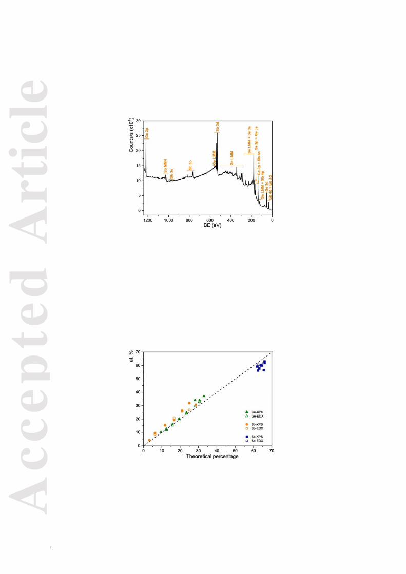
were compared to EDS data. Fig. 1 shows an example of typical XPS survey spectrum of as-
deposited thin film (Ge23.5Sb11.8Se64.7, i.e. x=20). The well-defined peaks are visible for Ge,
Sb and Se core level as well as Auger lines (Ge LMM, Sb MNN and Se LMM). No elements
Acc
epte
d A
rtic
le
.
other than the thin films’ components and residual oxygen were observed in all the
(GeSe2)100-x(Sb2Se3)x thin films’ XPS survey spectra.
Table I presents the chemical composition data of the as-deposited thin films from
(GeSe2)100-x(Sb2Se3)x system determined by EDS in comparison with parent glass targets.
Consequently, the chemical composition of PLD films was studied by XPS and compared to
EDS values (Fig. 2). For all the Ge-Sb-Se compositions under study, the agreement between
these two methods is fine and very similar general behavior is observed. Thereby, a
deficiency in chalcogen content (lower than 4 at. %) and an excess of antimony were
observed in comparison with glass targets real composition. The loss of selenium is probably
caused by its high volatility compared to germanium and antimony. In the case of
germanium, when its content is lower than ≈ 25 at. %, the agreement between the
composition of the films and theoretical one is very good as shown in Fig. 2. For higher Ge
content, small excess of this element in the films is observed.
The bonding characteristics of as-deposited (GeSe2)100-x(Sb2Se3)x (x values varying
from 0 to 60) thin films were studied by analyzing the core level XPS spectra taking into
account earlier papers25, 33, 34
. Fig. 3 (a, b, c) shows the Sb 4d and Ge 3d core level spectra for
films with x=5, x=20 and x=60. The binding energy (BE, eV), the full width at half
maximum (FWHM, eV) and the proportion of bonds (%) of the different components used
for the fitting of core level spectra of as-deposited thin films are presented in Table II. As
expected due to the chemical composition, the Sb core-level spectra area increases with the
introduction of antimony (or increase of x value) and a corresponding decrease in the area of
Ge core-level spectra is observed.
The Ge 3d core-level spectra presents a primary component at ≈ 30.30 eV (±0.05 eV).
Additional doublets have to be introduced to correctly fit the Ge 3d core-level spectra, one
with lower BE value (from 29.57 to 30.04 eV) and one with higher BE value (from 31.40 to

Acc
epte
d A
rtic
le
.
31.64 eV). The different BE of each structural units is determined by the neighboring atom
electronegativity. Accordingly, the binding energy downshift will be larger when the
difference of neighboring atom electronegativity is larger. From the electronegativities of Ge,
Sb and Se (2.01, 2.05 and 2.55 respectively in view of Pauling scale), the chemical
environments can be deduced. The primary component at ≈30.30 eV is assigned to the
regular Ge-(Se)4 environment corresponding to [GeSe4/2] tetrahedra. The doublet observed at
lower BE (from 29.57 to 30.04 eV) should be attributed to the (Ge,Sb)-Ge-(Se)3 environment
i.e. to a distorted tetrahedra where one Se atom is substituted with Ge or Sb atom (because of
their very similar electronegativities) forming M-M bonds. Finally, the doublet at higher BE
value (from 31.40 to 31.64 eV) is attributed to the oxide (Sey)-Ge-Ox because of the high
electronegativity of O (3.44)25
.
In analogy, three doublets are used to describe the Sb 4d core-level spectra. The
primary component is located from 32.66 to 32.78 eV and is attributed to the regular Sb-(Se)3
arrangement of [SbSe3/2] trigonal pyramid. M-M bonds are also observed with the second
doublet located at lower BE (from 32.23 to 32.65 eV) and attributed to (Ge,Sb)-Sb-(Se)2
environment. As in the case of Ge 3d core-level spectra, a third doublet is used to correctly fit
the Sb 4d core-level spectra of as-deposited thin films and it is attributed to (Sey)-Sb-Ox (at
34.02 eV)25, 34
. However, (Sey)-Sb-Ox is clearly observed for only (GeSe2)70(Sb2Se3)30 as-
deposited thin film (Table II).
Fig. 4a shows normalized core level band of Sb 4d – Ge 3d for (GeSe2)100-x(Sb2Se3)x
thin films, dashed lines correspond to the binding energies associated to the different entities
considered of x=10 sample which was used for the calibration. A slight shift towards higher
energies can be observed with the introduction of antimony. In detail, in Ge 3d core level
spectra, the doublet attributed to (Ge,Sb)-Ge-(Se)3 binding arrangement is shifted from 29.57
eV (x=5) to 29.99 eV (x=60). Likewise the doublet in the Sb 4d core level spectra, which is

Acc
epte
d A
rtic
le
.
attributed to (Ge,Sb)-Sb-(Se)2 binding arrangement, is shifted from 32.23 eV (x=5) to 32.65
eV (x=60).
The presence of M-M bonds (M = Ge, Sb) was also demonstrated for bulk Ge-Sb-Se
glasses7, 31, 34
and thin films6, 23, 33
. Sati et al34
used an additional doublet to fit Sb 4d core
level (at ≈ 32.20 ± 0.05 eV) which was attributed to a distorted Sb-based trigonal pyramid
with substitution of two and more Se atoms by Ge or Sb atoms34
. Further, an additional
doublet was used to fit the Ge 3d core level spectra at ≈ 29.90 ± 0.05 eV in Ge28Sb12Se60 and
Ge32Sb8Se60 glasses; this doublet was assigned to (Ge,Sb)2-Ge-(Se)2 bonding arrangement34
.
In contrast with this XPS analysis of Ge-rich SbxGe40-xSe60 glasses34
, the mentioned
additional doublet associated to Sb and Ge entities with a substitution of two and more Se
atoms by Ge or Sb atoms were not required for the description of Sb 4d – Ge 3d core level
spectra in this work.
As results from XPS data analysis performed in this study, the proportion of Sb-(Se)3
arrangements increases from 3.9 at.% (for x=5) to 28.4 at.% (for x=60) and the proportion of
Ge-(Se)4 arrangements decreases from 33.1 at.% (for x=0) to 7.9 at.% (for x=60) (Table 2).
These values confirm that the amorphous network of as-deposited thin films slowly evolves
from a [GeSe4/2] tetrahedra dominated structure to a [SbSe3/2] trigonal pyramidal one.
Furthermore, the proportion of (Ge,Sb)-Sb-(Se)2 bonds ranges from 6.5 to 21 % (from x=5 to
20) and then this proportion decreases to 7.5 % (x=60) (Table II). Similarly, the proportion of
(Ge,Sb)-Ge-(Se)3 bonds increases from 10.3 to 29.5 % from x=0 to 50 and then decreases to
16.6 % for x=60 (Table II). The lower value observed for x=30 film could be related to more
important amount of (Sey)-Sb-Ox (11.7 %) and (Sey)-Ge-Ox (5.8 %) bonds at the surface of
the films. Fig. 5 presents the M-M bonds proportions (at. %) i.e. Ge-Ge, Sb-Sb and Ge-Sb
bonds observed in Ge3d and Sb4d core level spectra. Introduction of antimony in thin films’
network leads to M-M bonds increase first due to (Ge,Sb)-Ge-(Se)3 and then to (Ge,Sb)-Sb-
Acc
epte
d A
rtic
le
.
(Se)2. The decrease of M-M bonds observed for x > 30 can be explained by the glass network
character which evolves to a network dominated by [SbSe3] pyramids (Table 2). Raman
analysis of PLD as-deposited thin film is somewhat different6. In fact, a decrease of Ge-Ge
bonds (at ≈ 170 and ≈ 270 cm-1
) is observed with the introduction of antimony in thin films
network. Furthermore, proportion of Sb-Sb bonds (at ≈ 155 cm-1
) seems to slightly increase
with x values and Raman spectra are dominated by Sb-Se (≈ 190 cm-1
) bonds for as-deposited
thin films with x>50.
In the case of XPS analysis of selenium, two doublets (3d5/2 and 3d3/2) were used to fit
correctly Se 3d core level spectra. Fig. 3 (d, e and f) illustrates fitting of Se 3d core level
spectra for x=5, 20 and 60. The Se 3d core level spectra presents a main component located
from 53.47 to 53.78 eV depending on composition which can be attributed to the (Ge,Sb)-Se-
(Ge,Sb) entities (Table 2). The second doublet, located from 54.02 to 54.35 eV, is assigned to
the Se-Se-(Ge,Sb) entities33, 34, 35
. A very slight shift towards lower energies was observed for
PLD films with the introduction of antimony as shown in Fig. 4b. Therefore Se-Se-(Ge,Sb)
and Se-(Ge,Sb)2 arrangements are shifted from 54.35 to 54.02 eV (from x=0 to x=40) and
from 53.75 to 53.47 eV (from x=5 to x=40) (Table 2). The content of (Ge,Sb)-Se-(Ge,Sb)
(80.8 – 89.9 %) and Se-Se-(Ge,Sb) (10.1 – 19.2 %) bonds is almost independent of
composition for all (GeSe2)100-x(Sb2Se3)x thin films (Table 2). Due to the comparable
electronegativities of Ge and Sb, the contributions from Ge and Sb are similar but not exactly
the same. Indeed, Sati et al.34
reported higher FWHM values for the two doublets attributed to
(Ge,Sb)-Se-(Ge,Sb) and Se-Se-(Ge,Sb) environments (0.8–0.9 eV) in comparison to doublets
of binary Ge-Se chalcogenide glasses (0.6-0.7 eV). In the case of Ge-Sb-Se sputtered thin
films, FWHM values of those doublets are also higher (0.9-1.0 eV)33
. In the line with
mentioned data, XPS bands of as-deposited PLD thin films present also higher FWHM values
(0.8-1.0 eV, Table 2), similar to Ge-Sb-Se bulk glasses and sputtered thin films.

Acc
epte
d A
rtic
le
.
Our previous XPS analysis33
performed with RF sputtered thin films with the nominal
composition Ge28.1Sb6.3Se65.6 (x=10) presents comparable proportion of M-M bonds as
follows. Considering the closest chemical composition of as-deposited PLD thin films (i.e.
comparison with the films sputtered at Ar pressure of 1.10-2
mbar), the proportion of (Ge,Sb)-
Ge-(Se)3 entities is about 14.1% (Table 2) and 12% for as-deposited PLD and sputtered thin
films, respectively. In the same way, the proportion of (Ge,Sb)-Sb-(Se)2 entities is about
11.5% (Table 2) and 9% for PLD and sputtered thin films, respectively. As mentioned above,
local structure analysis of (GeSe2)100-x(Sb2Se3)x bulk glasses7, PLD
6 and sputtered thin films
33
(for x=10 and x=50) using Raman spectroscopy has been previously reported. The presence
of homopolar Ge-Ge bonds in Ge2Se6/2 and Ge-GemSe4-m (m = 1,2,3,4) species and Sb-
Sb(Ge) bonds of Se2Sb-Sb(Ge)Se2(3) structural units in PLD films was confirmed by Raman
spectroscopy.
On the other hand, M-M bonds proportion seems to be to some extent overestimated
by XPS analysis for as-deposited PLD thin films with the nominal composition
Ge12.5Sb25Se62.5 (x=50). In fact, the proportion of (Ge,Sb)-Ge-(Se)3 entities is about 29.5%
(Table II) and 7% for as-deposited PLD and sputtered thin films, respectively. Further, the
proportion of (Ge,Sb)-Sb-(Se)2 entities is about 15.0% (Table II) and 0% for PLD and
sputtered thin films, respectively. This is consistent with Raman analysis of sputtered thin
films33
which demonstrates that for higher Ar pressure, the M-M bonds are almost not
observed. If we consider the Raman spectroscopy data for sputtered film deposited with Ar
pressure lower than 1.10-2
mbar, the spectrum of PLD film (x=50) looks like Raman spectra
of such sputtered films. The PLD film Raman spectrum shape is between those of two
sputtered films (7.5.10-3
and 5.10-3
mbar). From XPS analysis, the proportion of (Ge,Sb)-Ge-
(Se)3 entities for these two sputtered films is 19% and 47%, respectively. The semi-
quantitative analysis of Raman spectra of PLD film (x=50) compared to sputtered films let

Acc
epte
d A
rtic
le
.
expect proportion of (Ge,Sb)-Ge-(Se)3 entities around 22-25%. Thus, the general agreement
between Raman and XPS analysis is good keeping in mind that only first ten nanometers are
probed by XPS. Although, it seems that there is a slight overestimation of (Ge,Sb)-Ge-(Se)3
entities by the XPS analysis of PLD film (x=50).
The BE values found for PLD layers are in good agreement with sputtered thin films’
XPS analysis: Ge-(Se)4 and Sb-(Se)3 entities are located at 30.29 and 32.71 eV and 30.37 and
32.73 eV for as-deposited PLD and sputtered thin films with the nominal composition
Ge28.1Sb6.3Se65.6 (x=10). For Sb-rich thin films, mentioned two main entities are located at
30.32 and 32.78 eV and 30.34 and 32.71 eV for as-deposited PLD and sputtered thin films,
again in very good agreement.
Likewise, Se-Se homonuclear bonds were also revealed in Raman and XPS analysis
of RF sputtered thin films with the nominal chemical composition Ge28.1Sb6.3Se65.6 (x=10)
and Ge12.5Sb25Se62.5 (x=50)33
. The comparison of PLD and sputtered layers with x=10 gives
the proportion of Se-Se-(Ge,Sb) entities about 13.6% (Table 2) and 14% for as-deposited
PLD and sputtered thin films (at 1.10-2
mbar Ar)33
, respectively. In layers with x=50, the
content of Se-Se-(Ge,Sb) entities is about 16.2% (Table 2) and 22% for as-deposited PLD
and sputtered (at 1.10-2
mbar) thin films, respectively. Binding energies revealed for PLD thin
films are also in agreement with those observed for RF sputtered thin films. For x=10 films,
Se-Se-(Ge,Sb) entities are located at 54.30 eV (Table 2) and 54.32 eV for as-deposited PLD
and sputtered (1.10-2
mbar Ar pressure) layers, respectively33
. For Sb-rich thin films (x=50),
these entities are situated at 54.06 eV (Table 2) and 54.10 eV for PLD and sputtered (1.10-2
mbar Ar pressure) layers, respectively33
. Raman data analysis of RF sputtered thin films also
revealed the presence of Se-Se bonds, especially for higher Ar pressure, with the amplitude
increase of the band located at ≈265 cm-1
33
. These results also agree with previous XPS data
obtained for RF sputtered thin film with the nominal composition Ge25Sb10Se65; the
Acc
epte
d A
rtic
le
.
proportion of Se-Se-(Ge,Sb) is about 13% (for 5.10-3
mbar) and 29% (for 5.10-2
mbar) 25
. The
proportion of Se-Se homonuclear bonds is surprisingly high in these both compositions (x=10
and x=50) close to stoichiometric composition or with deficit in chalcogen element as shown
in Table I with relatively low content of M-M bonds. As it was already mentioned in previous
work25, 33
, another contribution to this second Se 3d core level component spectrum might be
considered: Se involved in bonds between two [GeSe4/2] tetrahedra connected by edges could
also contribute to Se-Se-(Ge,Sb) component.
It is worthy to mention that other techniques were already used for the structural analysis of
Ge-Sb-Se glasses, for example neutron diffraction, X-ray diffraction or extended X-ray fine
structure analysis. Pethes et al.36
used the reverse Monte-Carlo simulation technique37
to
investigate Ge20Sb5Se75, Ge20Sb15Se65 and Ge20Sb20Se60 glasses. All three glass compositions
show a structure mostly described by the chemically ordered network model in which Ge-Se
and Sb-Se bonds are preferred. For calculations using the reverse Monte Carlo method,
homopolar Se-Se bonds in Se-poor glass and M-M bonds in Se-rich glass are not needed
which is distinctive to the analysis performed by XPS spectroscopy for physical vapor
deposited Ge-Sb-Se films. However, the rapid quenching during the synthesis of the thin
films is likely to generate more defects than parent glasses and deviate from a perfect
chemically ordered network model.
IV. Conclusion
In this paper, amorphous chalcogenide thin films with the nominal composition (GeSe2)100-
x(Sb2Se3)x (x = 0, 5, 10, 20, 30, 40, 50 and 60) were deposited by PLD with chemical
composition relatively close to the targets’ composition. Nevertheless, EDX and XPS
analysis, performed on glass targets and as-deposited thin films, reveals a small deficit in

Acc
epte
d A
rtic
le
.
chalcogen element (Se) and an excess of Sb in the PLD films. The as-deposited thin films
were characterized by X-rays photoelectron spectroscopy in order to describe bonding
arrangement at the surface films. XPS investigations confirm the presence of the two main
regular units Ge-(Se)4 and Sb-(Se)3. The Sb core level spectra amplitude increases logically
with introduction of antimony so the amorphous network of as-deposited thin films slowly
evolves from a [GeSe4/2] tetrahedra dominated structure to a [SbSe3/2] pyramidal one. The
(Ge,Sb)-Ge-(Se)3 and (Ge,Sb)-Sb-(Se)2 environments, corresponding to distorted tetrahedra
or trigonal pyramid where one chalcogen element is substituted with Ge or Sb atom(s)
forming M-M bonds, were also observed. The proportion of M-M bonds increases with the
introduction of antimony (from x=0 to x=40) first due to (Ge,Sb)-Ge-(Se)3 and then thanks to
(Ge,Sb)-Sb-(Se)2 entities’ appearance. The study of Se 3d core level spectra reveals the
presence of two entities: (Ge,Sb)-Se-(Ge,Sb) and Se-Se-(Ge,Sb). XPS analysis of as-
deposited thin films seems to overestimate Se-Se homonuclear bonds, thus this component
could contain also Se involved in two [GeSe4/2] tetrahedra connected by edges.
Acknowledgments
This work was financially supported by the Czech Science Foundation (Project No. 16-
17921S). This work was also supported by the grants LM2015082, CZ.1.05/4.1.00/11.0251
and Barrande 7AMB17FR058 project from the Czech Ministry of Education, Youth and
Sports of the Czech Republic and PHC-Barrande (2017-2018) from French Ministery of
Education and Research.

Acc
epte
d A
rtic
le
.
References
1. Zhang, X. H., Bureau, B., Lucas, P., et al., "Glasses for seeing beyond visible," Chemistry-a
European Journal, 14[2] 432-42 (2008).
2. Vigreux-Bercovici, C., Ranieri, V., Labadie, L., et al., "Waveguides based on Te2As3Se5 thick
films for spatial interferometry," J. Non-Cryst. Solids, 352[23-25] 2416-19 (2006).
3. Meneghini, C. and Villeneuve, A., "As2S3 photosensitivity by two-photon absorption: holographic
gratings and self-written channel waveguides," Journal of the Optical Society of America B-
Optical Physics, 15[12] 2946-50 (1998).
4. Shimakawa, K., Kolobov, A., and Elliott, S. R., "Photoinduced effects and metastability in
amorphous semiconductors and insulators," Advances in Physics, 44[6] 475-588 (1995).
5. Nemec, P., Zhang, S., Nazabal, V., et al., "Photo-stability of pulsed laser deposited GexAsySe100-
x-y amorphous thin films," Opt. Express, 18[22] 22944-57 (2010).
6. Olivier, M., Nemec, P., Boudebs, G., et al., "Photosensitivity of pulsed laser deposited Ge-Sb-Se
thin films," Optical Materials Express, 5[4] 781-93 (2015).
7. Olivier, M., Tchahame, J. C., Nemec, P., et al., "Structure, nonlinear properties, and
photosensitivity of (GeSe2)(100-x)(Sb2Se3)(x) glasses," Optical Materials Express, 4[3] 525-
40 (2014).
8. Liu, Q. M., Zhao, X. J., Tanaka, K., et al., "Second-harmonic generation in Ge-As-S glasses by
electron beam irradiation and analysis of the poling mechanism," Opt. Commun., 198[1-3]
187-92 (2001).
9. Harbold, J. M., Ilday, F. O., Wise, F. W., et al., "Highly nonlinear Ge-As-Se and Ge-As-S-Se
glasses for all-optical switching," Ieee Photonics Technology Letters, 14[6] 822-24 (2002).
10. Lenz, G., Zimmermann, J., Katsufuji, T., et al., "Large Kerr effect in bulk Se-based chalcogenide
glasses," Opt. Lett., 25[4] 254-56 (2000).
Acc
epte
d A
rtic
le
.
11. Guignard, M., Nazabal, V., Smektala, F., et al., "Chalcogenide glasses based on germanium
disulfide for second harmonic generation," Advanced Functional Materials, 17[16] 3284-94
(2007).
12. Caillaud, C., Gilles, C., Provino, L., et al., "Highly birefringent chalcogenide optical fiber for
polarization-maintaining in the 3-8.5 mu m mid-IR window," Opt. Express, 24[8] 7977-86
(2016).
13. Caillaud, C., Renversez, G., Brilland, L., et al., "Photonic Bandgap Propagation in All-Solid
Chalcogenide Microstructured Optical Fibers," Materials, 7[9] 6120-29 (2014).
14. Pagani, M., Vu, K., Choi, D. Y., et al., "Instantaneous microwave frequency measurement using
four-wave mixing in a chalcogenide chip," Opt. Commun., 373 100-04 (2016).
15. Novak, S., Singh, V., Monmeyran, C., et al., "Positron annihilation lifetime spectroscopy (PALS)
studies of gamma irradiated As2Se3 films used in MIR integrated photonics," Journal of Non-
Crystalline Solids, 455 29-34 (2017).
16. Gutierrez-Arroyo, A., Baudet, E., Bodiou, L., et al., "Optical characterization at 7.7 mu m of an
integrated platform based on chalcogenide waveguides for sensing applications in the mid-
infrared," Opt. Express, 24[20] 23109-17 (2016).
17. Starecki, F., Charpentier, F., Doualan, J. L., et al., "Mid-IR optical sensor for CO2 detection based
on fluorescence absorbance of Dy3+:Ga5Ge20Sb10S65 fibers," Sensors and Actuators B-
Chemical, 207 518-25 (2015).
18. Michel, K., Bureau, B., Boussard-Pledel, C., et al., "Monitoring of pollutant in waste water by
infrared spectroscopy using chalcogenide glass optical fibers," Sensors and Actuators B-
Chemical, 101[1-2] 252-59 (2004).
19. Keirsse, J., Boussard-Pledel, C., Loreal, O., et al., "IR optical fiber sensor for biomedical
applications," Vib. Spectrosc., 32[1] 23-32 (2003).
20. Eggleton, B. J., Luther-Davies, B., and Richardson, K., "Chalcogenide photonics," Nat. Photonics,
5[3] 141-48 (2011).

Acc
epte
d A
rtic
le
.
21. Gai, X., Madden, S., Choi, D. Y., et al., "Dispersion engineered Ge11.5As24Se64.5 nanowires
with a nonlinear parameter of 136W(-1)m(-1) at 1550nm," Opt. Express, 18[18] 18866-74
(2010).
22. Shportko, K., Kremers, S., Woda, M., et al., "Resonant bonding in crystalline phase-change
materials," Nature Materials, 7[8] 653-58 (2008).
23. Chen, Y., Shen, X., Wang, R. P., et al., "Optical and structural properties of Ge-Sb-Se thin films
fabricated by sputtering and thermal evaporation," J. Alloys Compd., 548 155-60 (2013).
24. Nazabal, V., Charpentier, F., Adam J-L., "Sputtering and Pulsed Laser Deposition for Near- and
Mid-Infrared Applications: A Comparative Study of Ge25Sb10S65 and Ge25Sb10Se65
Amorphous Thin Films," International Journal of Applied Ceramic Technology, 8 990-1000
(2011).
25. Verger, F., Nazabal, V., Colas, F., et al., "RF sputtered amorphous chalcogenide thin films for
surface enhanced infrared absorption spectroscopy," Opt. Mater. Express, 3[12] 2112-31
(2013).
26. Musgraves, J. D., Carlie, N., Hu, J., et al., "Comparison of the optical, thermal and structural
properties of Ge-Sb-S thin films deposited using thermal evaporation and pulsed laser
deposition techniques," Acta Mater., 59[12] 5032-39 (2011).
27. Nazabal, V., Cathelinaud, M., Shen, W., et al., "Chalcogenide coatings of Ge15Sb20S65 and
Te20As30Se50," Appl. Optics, 47[13] C114-C23 (2008).
28. Charrier, J., M-L. Brandily, H. Lhermite, K. Michel, B. Bureau, F. Verger, V. Nazabal,
"Evanescent wave optical micro-sensor based on chalcogenide glass," Sensors and Actuators
B-Chemical, 173 468-76 (2012).
29. Ganjoo, A., Jain, H., Yu, C., et al., "Planar chalcogenide glass waveguides for IR evanescent wave
sensors," Journal of Non-Crystalline Solids, 352[6-7] 584-88 (2006).
30. Haisty, R. W. and Krebs, H., "ELECTRICAL CONDUCTIVITY AND FORMATION OF
CHALCOGENIDE GLASSES IN GE-AS-SE AND GE-SB-SE MELTS," Angew. Chem.-Int.
Edit., 7[12] 947-48 (1968).

Acc
epte
d A
rtic
le
.
31. Wei, W. H., Xiang, S., Xu, S. W., et al., "Structural investigation on GexSb10Se90-x glasses
using x-ray photoelectron spectra," J. Appl. Phys., 115[18] 183506 (2014).
32. Ai, Z. P. and earth, R., "Luminescence of In2S3 nanocrystallites embedded in sol-gel silica
xerogel," Optical Materials, 24[3] 589-93 (2003).
33. Baudet, E., Cardinaud, C., Girard, A., et al., "Structural analysis of RF sputtered Ge-Sb-Se thin
films by Raman and X-ray photoelectron spectroscopies," J. Non-Cryst. Solids, 444 64-72
(2016).
34. Sati, D. C., Kovalskiy, A., Golovchak, R., et al., "Structure of SbxGe40-xSe60 glasses around
2.67 average coordination number," Journal of Non-Crystalline Solids, 358[2] 163-67 (2012).
35. Chen, Y., Xu, T. F., Shen, X., et al., "Optical and structure properties of amorphous Ge-Sb-Se
films for ultrafast all-optical signal processing," J. Alloy. Compd., 580 578-83 (2013).
36. Pethes, I., Chahal, R., Nazabal, V., et al., "Chemical Short-Range Order in Selenide and Telluride
Glasses," J. Phys. Chem. B, 120[34] 9204-14 (2016).
37. McGreevy, R. L. and Pusztai, L., "REVERSE MONTE CARLO SIMULATION: A NEW
TECHNIQUE FOR THE DETERMINATION OF DISORDERED STRUCTURES," Mol.
Simul., 1[6] 359-67 (1988).
Acc
epte
d A
rtic
le
.
Figure captions
Fig 1. Survey XPS spectrum of Ge23.5Sb11.8Se64.7 (x=20) as-deposited thin film.
Fig. 2. Comparison of chemical composition of (GeSe2)100-x(Sb2Se3)x PLD films determined
by EDS (±1 %) and XPS (±1 %) analysis compared to theoretical composition.
Fig. 3. XPS spectra of as-deposited (GeSe2)100-x(Sb2Se3)x PLD thin films. Data fitting of Ge
3d and Sb 4d core level bands: a) x=5, b) x=20 and c) x=60; data fitting of Se 3d core level
bands: d) x=5, e) x=20 and f) x=60. Being very weak, the Sey-Ge-Ox components are not
shown in the curves fitting.
Fig. 4. Normalized core level band of Ge 3d – Sb 4d (a) and Se 3d (b) of (GeSe2)100-
x(Sb2Se3)x PLD thin films. Dashed lines correspond to the binding energy (BE, eV) of the
sample used for the calibration (x=10).
Fig. 5. M-M bonds (M = Ge, Sb) proportions (at. %, ±1 %) in Ge 3d and Sb 4d core level
spectra depending of x values in (GeSe2)100-x(Sb2Se3)x PLD thin films (dashed curve
corresponds to the overall trend of M-M bonds as a function of x values).

Acc
epte
d A
rtic
le
.
Tables
Table I. Theoretical and real chemical composition (at. %) determined by EDS for chalcogenide glass targets (GeSe2)100-x(Sb2Se3)x (±0.5 %)
and corresponding thin films prepared by pulsed laser deposition (±1 %).
Theoretical composition Target composition Thin film composition
%Ge %Sb %Se %Ge %Sb %Se %Ge %Sb %Se
x=0 33.3 - 66.7 36.5 - 63.5 39 - 61
x=5 30.6 3.2 66.1 31.0 3.4 65.6 33 4 63
x=10 28.1 6.3 65.6 28.3 6.8 64.9 30 8 62
x=20 23.5 11.8 64.7 23.1 13.0 63.9 24 15 61
x=30 19.4 16.7 63.9 19.5 17.8 62.7 19 21 60
x=40 15.8 21.1 63.2 14.9 22.3 62.8 15 26 59
x=50 12.5 25.0 62.5 12.1 25.4 62.5 13 27 61
x=60 9.5 28.6 61.9 10.4 29.1 60.5 9 29 62

Acc
epte
d A
rtic
le
.
Table II. Binding energy (BE, eV, ±0.05eV), full width at half maximum (FWHM, eV, ±0.05eV), proportion of bonds (%bonds, ±1%) and atomic
ratio (%at, ±1%) of the different components used for the fitting of Se 3d5/2, Ge 3d5/2, Sb 4d5/2 and Sb 3d5/2 core level spectra of as-deposited
(GeSe2)100-x(Sb2Se3)x thin films prepared by pulsed laser deposition.
Core
Level Se 3d5/2 Ge 3d5/2 Sb 4d5/2
Species Se-(Ge,Sb)2 Se-Se-(Ge,Sb) Ge-(Se)4 (Ge,Sb)-Ge-(Se)3 Sey-Ge-Ox Sb-(Se)3 (Ge,Sb)-Sb-(Se)2 Sey-Sb-Ox
x=0
BE (eV) 53.78 54.35 30.32 30.04 - - - -
FWHM 0.82 0.82 0.94 0.94 - - - -
% bonds 84 16 90 10 - - - -
% at 53 10 33 4 - - - -
x=5
BE (eV) 53.75 54.24 30.29 29.57 31.49 32.69 32.23 -
FWHM 0.94 0.94 1.03 1.03 1.03 1.00 1.00 -
% bonds 83 17 95 4 1 93 7 -
% at 51 11 32 1 1 4 1
x=10
BE (eV) 53.75 54.30 30.29 29.62 31.40 32.71 32.25 -
FWHM 0.96 0.96 0.98 0.98 0.98 1.01 1.01 -
% bonds 86 14 80 14 6 88 12 -
% at 49 8 27 5 2 9 1 -
x=20
BE (eV) 53.56 54.08 30.20 29.63 31.45 32.66 32.22 -
FWHM 0.93 0.93 0.92 0.92 0.92 0.88 0.88 -
% bonds 90 10 81 18 1 79 21 -
% at 54 6.0 20 4 1 12 3 -
x=30
BE (eV) 53.60 54.22 30.28 29.89 31.48 32.70 32.47 34.02
FWHM 0.93 0.93 0.85 0.85 0.85 0.86 0.86 1.28
% bonds 81 19 80 14 6 70 18 12
% at 49 12 16 3 1 14 3 2
x=40
BE (eV) 53.47 54.02 30.21 29.96 31.61 32.68 32.38 -
FWHM 0.88 0.88 0.94 0.94 0.94 0.86 0.86 -
% bonds 83 17 75 24.8 0 83 17 -
% at 48 10 12 4 0.0 22 5 -

Acc
epte
d A
rtic
le
.
x=50
BE (eV) 53.56 54.06 30.32 29.85 31.61 32.78 32.41 -
FWHM 0.82 0.82 0.75 0.75 0.75 0.87 0.87 -
% bonds 84 16 60 29 11 85 15 -
% at 47 9 7 4 1 27 5 -
x=60
BE (eV) 53.58 54.15 30.35 29.99 31.64 32.78 32.65 -
FWHM 0.84 0.84 0.82 0.82 0.82 0.84 0.84 -
% bonds 83 17 79 17 5 92 8 -
% at 49 10 8 2 1 28 2 -
Acc
epte
d A
rtic
le
.

Acc
epte
d A
rtic
le
.

Acc
epte
d A
rtic
le
.