Embed Size (px)
Citation preview


:
I
US B
I
M5B?fl
I I .v ^•:„;-t -:iWv tfsiof
JrvflBPD

,< '..1,
^CAU Of *
NBS TECHNICAL NOTE 688
U.S. DEPARTMENT OF COMMERCE / National Bureau of Standards
Yagi Antenna Design
NEW BOOK SHELF
JAN 3 1 1977

NATIONAL BUREAU OF STANDARDS
The National Bureau of Standards 1 was established by an act of Congress March 3, 1901.The Bureau's overall goal is to strengthen and advance the Nation's science and technologyand facilitate their effective application for public benefit. To this end, the Bureau conductsresearch and provides: (1) a basis for the Nation's physical measurement system, (2) scientific
and technological services for industry and government, (3) a technical basis for equity in trade,
and (4) technical services to promote public safety. The Bureau consists of the Institute for
Basic Standards, the Institute for Materials Research, the Institute for Applied Technology,the Institute for Computer Sciences and Technology, and the Office for Information Programs.
THE INSTITUTE FOR BASIC STANDARDS provides the central basis within the UnitedStates of a complete and consistent system of physical measurement; coordinates that system
with measurement systems of other nations; and furnishes essential services leading to accurate
and uniform physical measurements throughout the Nation's scientific community, industry,
and commerce. The Institute consists of the Office of Measurement Services, the Office of
Radiation Measurement and the following Center and divisions:
Applied Mathematics — Electricity — Mechanics — Heat — Optical Physics — Center
for Radiation Research: Nuclear Sciences; Applied Radiation — Laboratory Astrophysics 2
— Cryogenics 2 — Electromagnetics - — Time and Frequency 2.
THE INSTITUTE FOR MATERIALS RESEARCH conducts materials research leading to
improved methods of measurement, standards, and data on the properties of well-characterized
materials needed by industry, commerce, educational institutions, and Government; provides
advisory and research services to other Government agencies; and develops, produces, and
distributes standard reference materials. The Institute consists of the Office of Standard
Reference Materials, the Office of Air and Water Measurement, and the following divisions:
Analytical Chemistry — Polymers — Metallurgy — Inorganic Materials — Reactor
Radiation — Physical Chemistry.
THE INSTITUTE FOR APPLIED TECHNOLOGY provides technical services to promote
the use of available technology and to facilitate technological innovation in industry and
Government; cooperates with public and private organizations leading to the development of
technological standards (including mandatory safety standards), codes and methods of test;
and provides technical advice and services to Government agencies upon request. The Insti-
tute consists of the following divisions and Centers:
Standards Application and Analysis — Electronic Technology — Center for Consumer
Product Technology: Product Systems Analysis; Product Engineering — Center for Building
Technology: Structures, Materials, and Life Safety; Building Environment; Technical Evalua-
tion and Application — Center for Fire Research: Fire Science; Fire Safety Engineering.
THE INSTITUTE FOR COMPUTER SCIENCES AND TECHNOLOGY conducts research
and provides technical services designed to aid Government agencies in improving cost effec-
tiveness in the conduct of their programs through the selection, acquisition, and effective
utilization of automatic data processing equipment; and serves as the principal focus within
the executive branch for the development of Federal standards for automatic data processing
equipment, techniques, and computer languages. The Institute consists of the following
divisions:
Computer Services — Systems and Software — Computer Systems Engineering — Informa-
tion Technology.
THE OFFICE FOR INFORMATION PROGRAMS promotes optimum dissemination and
accessibility of scientific information generated within NBS and other agencies of the Federal
Government; promotes the development of the National Standard Reference Data System and
a system of information analysis centers dealing with the broader aspects of the National
Measurement System; provides appropriate services to ensure that the NBS staff has optimum
accessibility to the scientific information of the world. The Office consists of the following
organizational units:
Office of Standard Reference Data — Office of Information Activities — Office of Technical
Publications — Library — Office of International Relations — Office of International
Standards.
1 Headquarters and Laboratories at Gaithersburg, Maryland, unless otherwise noted; mailing address
Washington. DC. 20234.
- Located at Boulder. Colorado 80302.

Yagi Antenna Design
Peter P. Viezbicke
Time and Frequency Division
Institute for Basic Standards
National Bureau of Standards
Boulder, Colorado 80302
*t*T 0F or
/ V
U.S. DEPARTMENT OF COMMERCE, Elliot L. Richardson, Secretary
Edward 0. Vetter, Under Secretary
Dr. Betsy Ancker-Johnson, Assistant Secretary for Science and Technology
NATIONAL BUREAU OF STANDARDS, Ernest Ambler, Acting Director
Issued December 1976

NATIONAL BUREAU OF STANDARDS TECHNICAL NOTE 688
Nat. Bur. Stand. (U.S.), Tech Note 688, 27 pages (December 1976)
CODEN: NBTNAE
U.S. GOVERNMENT PRINTING OFFICE
WASHINGTON: 1976
For sale by the Superintendent of Documents, US Government Printing Office, Washington, DC. 20402
(Order by SD Catalog No. C13. 46:688) Price 65 cents (Add 25 percent additional for other than U.S. mailinj
FOREWORD
This work was carried out by the NationalBureau of Standards at antenna test ranges
located in Sterling, Virginia, and at TableMountain near Boulder, Colorado.
These measurements were carried out by the
Antenna Research Section of the Radio SystemDivision, National Bureau of Standards.
I i


CONTENTS
1. INTRODUCTION
2. METHOD OF MEASUREMENT
3. RESULTS
3.1 Effect of Reflector Spacing on Measured Gain
3.2 Effect of Different Equal Length Directors and
for Different Yagi Lengths
Spac ng on Measured Gain
3.3 Effect of Different Diameters and Lengths of Directors on Measured Gain
3.4 Effect of the Size of a Supporting Boom on the Optimum Length of a
Parasitic Element ..........3.5 Effect of Spacing and Stacking of Yagi Antennas on Realizable Gain
3.6 Measured Radiation Patterns of Different Length Yagi Antennas
k. DESIGNING THE YAGI ANTENNA
5. CONCLUSIONS
6. ACKNOWLEDGMENTS ....7. REFERENCES
Page
1
1
1
2
6
6
6
16
21
21
21
LIST OF TABLES and FIGURES
Table 1. Optimized Lengths of Parasitic Elements for Yagi Antennas of SixDifferent Lengths ..........
Figure 1. Gain in dB of a Dipole and Reflector for Different Spacings BetweenElements ...........
Figure 2. Arrangement of Three Reflecting Elements Used With the k.2X Yagi
Figure 3. Photograph of the Trigonal Reflector Experimental Set-Up Used Withthe k.2\ Yagi
Figure k. Gain of a Yagi as a Function of Length (Number of Directors) for
Different Constant Spa. igs Between Directors of Length Equal to
0.382X .
Figure 5- Gain of a Yagi as a Function of Length (Number of Directors) for
Different Constant Spacings Between Directors of Length Equal to
0.41 U .
Figure 6. Gain of a Yagi as a Function of Length (Number of Directors) forDifferent Constant Spacings Between Directors of Length Equal to
O.klkX .-..."

Figure 7.
Figure 8.
Figure 9-
Figure 10.
Figure 1 1
.
Figure 12.
Figure 13.
Figure ]k.
Figure 15.
Fi gure 16.
Figure 17.
Figure 18.
Figure 19.
Figure 20.
Figure 21
,
Comparison of Gain of Different Length Yagis Showing the RelationshipBetween Directors Optimized in Length to Yield Maximum Gain andDirectors of Optimum Uniform Length .......Measured Gain Vs Director Length of a 1.25A Yagi Antenna Using ThreeDirectors of Different Length and Diameter Spaced 0.35A.
Yagi Antenna Design Data Showing the Relationship Between ElementDiameter to Wavelength Ratio and Element Length for Different Antennas
Graph Showing the Effect of a Supporting Boom on Length of Elements
Gain of an Array of Yagis, Stacked One Above the Other and in Broadsas a Function of Spacing ......Gain of an Array of Two Sets of Stacked Yagis Spaced 1 .6X as a functof Horizontal Distance Between Them .....Radiation Patterns of a Dipole and Reflector With 0.2A Spacing
Radiation Patterns of a 3~Element, 0.k\ Long Yagi
Radiation Patterns of a 5-Element, 0.8A Long Yagi
Radiation Patterns of a 6-Element, 1.2A Long Yagi
Radiation Patterns of a 12-Element, 2.2X Long Yagi
Radiation Patterns of a 17-Element, 3.2X Long Yagi
Radiation Patterns of a 15 - Element, 4.2X Long Yagi
Use of Design Curves in Determining Element Lengths of 0.8X Yag
Considered in Example 1 .......Use of Design Curves in Determining Element Lengths of h.2X Yag
Considered in Example 2 .......
de
,
on
8
8
9
10
11
11
12
12
13
13
l*t
14
15
20
VI

YAGI ANTENNA DESIGN
Peter P. Viezbicke
This report presents data, using modeling techniques, for the optimum design
of different length Yagi antennas. This information is presented in graphical
form to facilitate the design of practical length antennas--f rom 0.2A to k.2X
long--for operation in the HF, VHF, and UHF frequency range. The effects of
different antenna parameters on realizable gain were also investigated and the
results are presented. Finally, supplemental data are presented on the stacking
of two or more antennas to provide additional gain.
Key words: Antenna, director, driven element, gain, radiation pattern, reflector,
Yagi.
1 . INTRODUCTION
The Yagi-Uda antenna [1], commonly known as the Yagi, was invented in 1926 by Dr. H. Yagi
and Shintaro Uda. Its configuration normally consists of a number of directors and reflectorsthat enhance radiation in one direction when properly arranged on a supporting structure.
Since its discovery, a large number of reports have appeared in the literature relativeto the analysis, design, and use of the Yagi antenna [2, 3, 4, 5, 6, 7, 8, 9], However,little or no data seem to have been presented regarding how parasitic element diameter,element length, spacings between elements, supporting booms of different cross sectionalarea, various reflectors, and overall length affect measured gain.
This report presents the results of extensive measurements carried out by the NationalBureau of Standards to determine these effects and gives graphical data to facilitate thedesign of different length antennnas to yield maximum gain. In addition, design criterionis also presented on stacki ng--one above the other and in a columnar configuration. Thegain is given in decibels (dB) relative to a dipole (reference antenna) at the same heightabove ground as the test (Yagi) antenna.
2. METHOD OF MEASUREMENT
The measurements were carried out at the NBS antenna range when it was located at
Sterling, Virginia, and at Table Mountain, Colorado, after the antenna research group wasrelocated to Colorado. All measurements were conducted at a modeling frequency of 400 MHz.
The antenna under test was used as a receiving antenna and was located approximately320 meters from a target transmitter and antenna. The transmitting antenna was located ata height above ground so that the receiving antennas were illuminated at grazing angles.The Yagi under test was mounted 3^ (wavelength) above ground and its gain was compared to
a reference dipole antenna located approximately 5A to one side and at the same height as
the test antenna. Each antenna was matched precisely to 50 ohms and switched alternatelyto an attenuator and associated receiving and detecting equipment located in a nearbywooden building. In comparing the attenuator readings of the two antennas to produce a
constant receiver output level, line losses to each were measured and compensated for in
arriving at final values of gain. The values of gain were reproducible to within 0.2 dBover the period when measurements were being carried out. The values presented are thosemeasured in a forward direction compared to the maximum response of a dipole at the sameheight above ground and are believed accurate to within 0.5 dB. If referenced to anisotropic source, the values must be increased by 2.16 dB.
3. RESULTS
The results of the measurements carried out in this study are presented in graphicalform. They are intended to provide a simple means of designing a Yagi antenna of practicaldimensions with maximum gain for the configuration under consideration. The purpose ofthese tests was to determine the following:

a. Effect of reflector spacing on the gain of a dipole antenna
b. Effect of different equal length directors, their spacing and number onreal izable gai n
c. Effect of different diameters and lengths of directors on realizable gain
d. Effect of the size of a supporting boom on the optimum length of parasiticel ements
e. Effect of spacing and stacking of antennas on gain
f. Measured radiation patterns of different Yagi configurations
3.1 EFFECT OF REFLECTOR SPACING ON MEASURED GAIN
These tests as well as all others were carried out on a non-conducting plexiglassboom mounted 3A above ground. With the exception of measurements stated in sections 3.3and 3-^, all parasitic elements were constructed of 0.63 cm (one-fourth inch) diameteraluminum tubing. The driven element used in the Yagi as well as in the reference dipolewas a half-wave folded dipole matched to 50 ohms using a double-stub tuner.
The gain of a dipole and reflector combination for different spacings between the twoelements is shown in figure 1. Maximum measured gain was 2.6 dB and was realized at a
spacing of 0.2A behind the dipole. This reflector spacing was used in all subsequentmeasurements. However, for the different Yagi configurations the reflector length wasoptimized to yield maximum gain. An additional 0.75 dB gain was realized using thereflector configuration shown in figure 2.
Although this arrangement was used only on the ^4 . 2X long Yagi, comparable benefitswould be realized with other antenna lengths. A photograph of the experimental set-up for
this configuration is shown in figure 3.
Various arrangements and spacings of reflector elements were tested on the k.2\ Yagi
using the drilled plexiglass support as shown. The reflecting elements were arranged in
shapes of plane reflecting surfaces, parabolas and corner reflectors. In addition,different shaped solid reflecting surfaces placed at various distances behind the drivenelement were also used. Of the combinations tested, the one shown in figure 2 yielded the
largest increase in gain over that of the single reflecting element.
3.2 EFFECT OF DIFFERENT EQUAL LENGTH DIRECTORS AND
SPACING ON MEASURED GAIN FOR DIFFERENT YAGI LENGTHS
These measurements were conducted using the same non-conducting boom as mentioned in
the preceding section. The driven element consisted of a A/2 folded dipole; the reflectorwas 0.^82X in length and spaced 0.2A behind the driven element. The diameter of all
elements was 0.0085A '(0.25 inches = 0.63cm).
The gain of the Yagi was measured as a function of antenna length (number of directors]for different equal length directors and spacing between them. The director lengths werevaried from 0.304A to 0.423A and spacings from 0.01A to 0.40X. The Yagi length, measuredfrom the driven element to the last director, was varied from an overall length of 0.2A to
10. 2X. The reflector in all cases was fixed. Although many measurements were carried out,only those results and associated graphs are presented that show the effects of theseparameters on measured gain.
Figures k, 5, and 6 show the relative gain of a Yagi as a function of length for
different spacings between director elements using director lengths of 0.382A, 0.^1 IX,
and O.kmX. Figure h shows that for relatively short directors at a spacing of 0.3X,
the gain of the Yagi increased to a maximum value of 14.5 dB when the antenna length was
increased to approximately 10A. Note, however, that as the spacing between elements was

oQ_
<
<
<oh-
UJ>
<_JLUEC
CO
<C3
/
t -©-
DE REFLECTOR
2A
^
_L
.05 .10 .15 .20 .25 .30 .35A
SPACING, S, OF REFLECTOR BEHIND DRIVEN ELEMENT
FIG. 1 GAIN IN dB OF A DIPOLE AND REFLECTOR FOR
DIFFERENT SPACINGS BETWEEN ELEMENTS
0.173A
©LR3 il
0.135A
DIRECTORS
DRIVENELEMENT
®LR3 0.27X
REFLECTOR LENGTHS
LR1 = LR2 = 0.455ALR3 = 0.473AFREQ = 400 MHz
[LENGTHS NOT CORRECTED FOR BOOM OR SUPPORT THICKNESS]
©'LR2
FIG. 2 ARRANGEMENT OF THREE REFLECTING ELEMENTS USED WITH THE 4.2X YAG
I

FIG. 3 PHOTOGRAPH OF THE TRIGONAL REFLECTOR EXPERIMENTAL
SET-UP USED WITH THE k . 2\ YAG
I
3: <->
LUO £3
0.3A SPACING
°- 0.4A SPACING
0.2X SPACING
0.06A SPACING
0.10X SPACING
/o 1
ADD 0.2XFOR REFL
2 3 4 5 6 7
LENGTH OF YAGI IN WAVELENGTHS
FIG. k GAIN OF A YAGI AS A FUNCTION OF LENGTH (NUMBER OF DIRECTORS)
FOR DIFFERENT CONSTANT SPACINGS BETWEEN DIRECTORS OF LENGTH
EQUAL TO 0.382X

ujO Q
12
a^i
10
9 /©3-c
8
1:1 y/V\ ^^X?\ o
6
• 0.1A SPACING
P0.2A \p. SPACING ^—SQ ^^
o
4
<
GAIN OF DIPOLE AND REFLECTOR
2
R
1l 1 1 l I
11 1 1
/"o
ADD 0. 2X
FOR REEL
2 3 4 5 6 7
LENGTH OF ANTENNA IN WAVELENGTHS
3X SPACING
0.4A SPACING
FIG. 5 GAIN OF A YAG I AS A FUNCTION OF LENGTH (NUMBER OF DIRECTORS',
FOR DIFFERENT CONSTANT SPACINGS BETWEEN DIRECTORS OF LENGTH
EQUAL TO 0.*tl U
12r-
UJO Q
/o 1
ADD 0.2AFOR REFL
2 3 4 5 6 7
LENGTH OF ANTENNA IN WAVELENGTHS
0.30X SPACING
FIG. 6 GAIN OF A YAG I AS A FUNCTION OF LENGTH (NUMBER OF DIRECTORS)
FOR DIFFERENT CONSTANT SPACINGS BETWEEN DIRECTORS OF LENGTH
EQUAL TO O.klkX

decreased, an oscillatory wave pattern resulted wherein the maximum gain occurred at a
shorter Yagi length and varied between a maximum and minimum value as the length of the Yag
i
was changed. As the length of the directors was increased, the variations in the wavepattern were also enhanced together with a reduction in gain as shown in figures 5 and 6.
The curves presented in figure 7 show a comparison of realized gain vs Yagi length upto k .2\ for antennas using directors of equal length and those optimized in length. For theoptimized length configurations the gain increased from 0.5 dB for the 2.2A. antenna to
approximately 1.5 dB for the 4.2A Yagi. Table 1 gives details of antenna parameters for the
different optimized design lengths tested and measured.
3.3 EFFECT OF DIFFERENT DIAMETERS AND LENGTHS OF DIRECTORS ON MEASURED GAIN
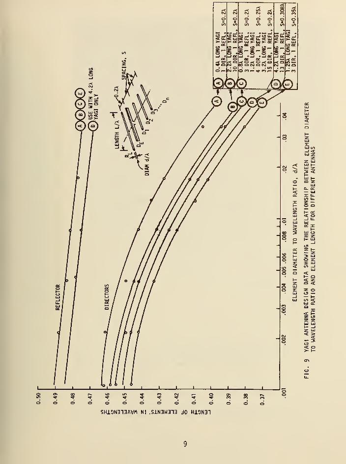
This effect was determined by measuring the gain of different Yagi configurations fordifferent director lengths of various diameters. Curves showing the results of measurementscarried out on the 1.25A long Yagi are given in figure 8. As expected, the maximum gain forthe different combinations remained unchanged. The larger diameter elements yielded maximumgain at shorter lengths while the smaller diameter elements yielded maximum gain at corre-spondingly greater lengths. Results of a series of measurements, noting these effects, werecarried out on the different length Yagis and, together with results presented in Table 1, a
set of design curves was produced and is presented in figure 9- These data provide the
basic design criterion of the Yagi antenna and are valid over a large frequency range providedthe selected element diameter to wavelength ratio d/X falls within the limits shown.
3. it EFFECT OF THE SIZE OF A SUPPORTING BOOM ON
THE OPTIMUM LENGTH OF A PARASITIC ELEMENT
Round and square supporting booms of different cross-section area were employed in
Yagi antennas of different lengths to determine what effect the boom diameter had on the
optimum length of the parasitic elements. The round and square booms yielded similar
results. The effect of a round supporting boom on the length of a parasitic element is
represented by the curve in figure 10. This experimental response can be used in applyingthe boom correction for the final Yagi design.
3.5 EFFECT OF SPACING AND STACKING OF YAGI ANTENNAS ON REALIZABLE GAIN
As shown in figure 11, additional gain is realized when antennas are stacked oneabove the other or in broadside. Not only is gain increased but the beamwidth is reduced
appreciably depending upon the configuration employed.
Figure 11 (A) shows the effects of stacking two antennas, one above the other. These
responses show similar mutual effects between two seven-element Yagis and between two
fifteen-element Yagis. At close spacing, approximately 0.8A, the gain was reduced due to
high mutual impedance effects but increased to a maximum of 2.5 dB as the spacing was
increased to approximately 1.6A. Similar effects were measured with the combination shown
in figure 11 (B) . Maximum gain in this case was realized with the two antennas spaced at
approximately 2.0A.
A combination of the above two configurations using spacings as shown yielded an
additional 2.5 dB gain and a corresponding reduction in beamwidth. For example, four 0.8A
Yagi antennas, appropriately stacked, spaced and fed in phase yielded a gain of 1^.2 dB
relative to a dipole located at the same height above ground. In contrast, a combinationof four 4.2A Yagi antennas yielded a gain of 19-6 dB relative to a dipole, as shown by the
graph in figure 12.
3.6 MEASURED RADIATION PATTERNS OF DIFFERENT LENGTH YAGI ANTENNAS
Radiation patterns measured in the E (hor i zontal -sol id curves) and H (vert ical -dashed
curves) planes for different Yagi designs are presented in figures 13 through 19. The
radiation patterns of the simplest yagi array (which consists of a reflector and driven

TABLE 1. OPTIMIZED LENGTHS OF PARASITIC ELEMENTS
FOR YAGI ANTENNAS OF SIX DIFFERENT LENGTHS
LENGTH OF YAGI IN WAVELENGTHS
0.4 0.8i
1 .20 2.2 3-2 4.2
LENGTH OF
REFLECTOR, A0.482 0.482 0.482 0.482 0.482 0.475
r<
1st 0.424 428 0.428 0.432 0.428 0.424
2nd 0.424 0.420 0.415 0.420 0.424
3rd 0.428 0.420 0.407 0.407 0.420
4th 0.428 0.398 0.398J
0.407
5th 0.390 0.394 0.403
6th 0.390 0.390 0.398
:ctof 7th 0.390 0.386 0.394
8th 0.390 0.386 0.390
fe 9th 0.398 O.386 0.390
1—oz 10th 0.407 0.386 0.390
_l11th
1
O.386 0.390
12th|
0.386 0.390
13th i
i
O.386 0.390
lAth O.386
15th O.386
SPACING BETWEENDIRECTORS, IN A
0.20 0.20 0.25 0.20 0.20 0.308!
GAIN RELATIVETO HALF-WAVEDIPOLE IN dB
7.1 9.2 10.2 12.25 13.4 14.2
DESIGN CURVE ! , v
(SEE FIG. 9)K (B)
~1
(B) (C)
1
i
(B) (D)
ELEMENT DIAMETER = O.OO85
f = 400 MHz
REFLECTOR SPACED C.2A BEHIND DRIVEN ELEMENT

o
<o
<CJ3
15
13
1 1-
10
© DIRECTOR LENGTHS OPTIMIZEDFOR MAXIMUM GAIN (SEE TABLE 1)
© DIRECTORS OF OPTIMUM UNIFORM LENGTH
N = NUMBER OF DIRECTORSS = SPACING BETWEEN DIRECTORS(REFLECTOR SPACED 0. 2A ON ALL ANTENNAS)
1.0 2.0 3.0 4.0
OVERALL LENGTH, IN WAVELENGTHS, OF DIFFERENT YAG I
S
5.0
oQ-
FIG. 7 COMPARISON OF GAIN OF DIFFERENT LENGTH YAG I S SHOWING THE
RELATIONSHIP BETWEEN DIRECTORS OPTIMIZED IN LENGTH TO YIELD
MAXIMUM GAIN AND DIRECTORS OF OPTIMUM UNIFORM LENGTH
><
<o
10
0.08 cm DIAMETER
1 in. = 2. 54 en
10 11 12 13
LENGTH OF DIRECTORS IN INCHES
14
FIG. 8 MEASURED GAIN VS DIRECTOR LENGTH OF A 1.25X YAG I ANTENNAUSING THREE DIRECTORS OF DIFFERENT LENGTH AND DIAMETER
SPACED 0.35X
in
co
»<
r< r<r<
»< to ,< s •<to
CM CM CM CM CM ro CO
o O OOO OII II II II II N HIS) CO CO CO CO CO
• p _>-« —
1
M * *-H » t—* |
5 d coCD _i CO U_ CD _l CD _l CD U. < —1< u. < LU <u.<u.<uj <£ UJ >-u.>- LU >- OC >- uj >- lu >- a: >- Ctf tu
oe CO ocu CD»— CO CD CD r— CD —o'
-»o "" "" « g .
Of—_l
_i • _1 OS _l • _) •-!« _1 anoe N4 ae ec >— 1—
1
*< OS^ s << Q -<«^l-i^Q >< IO •—«ON CO O CM Q CM CM CM O• • to • enOr- CM «— O CO 1— «fr co 1— Wf— «— CO
<ji oU 0) /oVfUj
ZUJ CO-l<UJ zzz UJLU h-LU 7:
g<c
LU 1-CO z
UJO- Qi— UJ3: U_CO U_z —Q
K- a:<_l li-
LUCd re
t-LUx: zl- LU
o 2:x: ujco _i
LU<I- Q< ZQ <Z OCD —— I-co <LU CCQ
a:< HZ CDz z
< ><— 3CD< O>- t-
OOOOOOOOSH19N313AVM Nl .S1N3W313 JO H1DN3T

COI-
LU
UJ
^1- Oo:c
r< 1—^v CJ3Q Z
UJ** _J
21O ZO OCO
3TO Oz O— cah-cc
CO O 2tO D_ __Q- \-^ ccCO
Q_Ll. Q_O ZD
COO— <rh-< Li_
en O31 h-r- OCD LU
a Z U.° LU U__l LULU> LU< n:3 h-
Oh- z.
o: ~sUJh- nzLU CO21< :n
,— Q_Q <
a:
Y 'S1N3W313 OlllSVUVd JO H19N31 WflWIldO Nl 3SV3yONI
10

o 2<>-
Ts
1.
7 ELEMENT YAGI ANTENNAS15 ELEMENT YAGI ANTENNAS
(A) VERTICAL SPACING, S IN WAVELENGTHS, BETWEEN ANTENNAS
< 2
-o- 7 ELEMENT YAGI ANTENNAS--•-15 ELEMENT YAGI ANTENNAS
I I
1 2 3
(B) HORIZONTAL SPACING, S IN WAVELENGTHS, BETWEEN ANTENNAS
FIG. 11 GAIN OF AN ARRAY OF YAG I S , STACKED ONE ABOVE THE OTHERAND IN BROADSIDE, AS A FUNCTION OF SPACING
lu 20
<
19
<o
<^ 17
16
<
4.2A LONG15 ELEMENT
YAGI
h = 2A
SPACING S = 1 .6A ANDHEIGHT h = 2.0A CONSTANT
>/XsX/K-X/W<WX^<sX'X\X//jy
t1.0 2.0 3.0
HORIZONTAL SPACING, H IN WAVELENGTHS, BETWEEN STACKED YAG I
S
FIG. 12 GAIN OF AN ARRAY OF TWO SETS OF STACKED YAG I S SPACED 1 . 6AAS A FUNCTION OF HORIZONTAL DISTANCE BETWEEN THEM
11

CO-o
oo.COCDCC
-oCL)
N
*rf ^K gs-::1
' -
~^\N
H PLANE-/
/
*T /T ........ N\\\
*E ;;;;
H
-
\ N /
\,f-
IU
1 _±
-
\A-^,
-E PLANE -
-
\-
-^
-
- -
90* 120"
Azimuthal Angle, degrees
FIG. 13 RADIATION PATTERNS OF A DIPOLE AND REFLECTOR WITH 0.2X SPACING
CO-o
oQ.1/1
<u
"OCDN
Azimuthal Angle, degrees
FIG. \k RADIATION PATTERNS OF A 3-ELEMENT, 0.4X LONG YAG
I
12

CO
CDOt
TDCD
CO
oQ-00a;
-aCDM
X- :
/•v
/// V W E
: 48* -1
\\
\JL' WH = 56'
v
11 : \\
y'\\
1
\i:::
i
j\\ f1/
\ \
\\ 1 V \y \\ \
1 \
\ \ 1 \
'"
\ \
\ \
\
ly~^
9
1
\
l/
\ i.
"
ii
ii \V
-
pi
Ii
1 -
-
Azimuthal Angle, degrees
FIG. 15 RADIATION PATTERNS OF A 5-ELEMENT, 0.8X LONG YAG
I
Azimuthal Angle, degrees
FIG. 16 RADIATION PATTERNS OF A 6-ELEMENT, 1.2X LONG YAG
I
13

CO
oQ.
CDQC
T3OlN
X3
oQ-l/>
CL)
a>N
Azimuthal Angle, degrees
FIG. 17 RADIATION PATTERNS OF A 12-ELEMENT, 2.2A LONG YAG
I
Azimuthal Angle, degrees
FIG. 18 RADIATION PATTERNS OF A 17-ELEMENT, 3.2A LONG YAG
I
14

en-a
oQ-coCD
CDISI
Azimuthal Angle, degrees
FIG. 19 RADIATION PATTERNS OF A 15-ELEMENT, k.2\ LONG YAG
15

element) are presented in figure 13. The 3~dB E and H plane beamwidths measured 66 and111° respectively. The beamwidth of the 3-element . ^X antenna, as shown in figure 1 4
,
measured 57 and 72 in the E and H planes respectively. The E plane, front-to-side ratiois in the order of 24 dB, while the radiation to the rear was only 8 dB down from that in
the forward direction.
The radiation pattern of the 5_element 0.8A Yag i presented in figure 15 is characterized
by a 3 dB beamwidth of 48 and 56 in the E and H planes respectively. The E plane,
front-to-side ratio remained comparable to the 3-element antenna; however, the front-to-
back ratio was improved considerably and measured 15 dB. In radiation patterns of 6, 12,
17 and 15-element Yagis as shown in figures 16 through 19, the beamwidths became progres-sively smaller as was expected with increased gain.
4. DESIGNING THE YAG I ANTENNA
To facilitate the design of an antenna of practical dimensions and yet realize maximumgain, refer to the curves shown in figure 9- These data were developed from results ofmodel measurements carried out at 400 MHz using elements of different diameters. Onlythose curves are presented which will enable the user to design the 0.4, 0.8, 1.2, 2.2,3.2 and 4.2A long Yagis that yield gains of 7.1, 9-2, 10.2, 12.3, 13.4 and 14.2 dB respec-tively over that of a dipole mounted at the same height above ground.
In designing a Yag i antenna, the following basic information is required and, of
course, will depend upon individual requirements.
1. Frequency of operation, f (wavelength, A)
2. Antenna gain required, G (dB)
3. Diameter of parasitic elements (directors-reflectors) used in construction, d/A
4. Diameter of supporting boom used in construction, D/A
Careful consideration should also be given to selection of the diameter of the
elements and boom at the wavelength or frequency of operation. This is important sincesmaller diameter and lighter materials can be used at the higher frequencies in contrastto larger and heavier materials needed for support at the lower frequencies. Note alsothat the selected element diameter-to-wavelength ratios used in the design of the chosenantenna must fall within the limits shown.
If maximum gain is to be realized using the data presented, it is essential to followvery closely the procedure described here. In addition, the element lengths should be
measured and cut to a tolerance of about 0.003A with respect to the calculated values. Toaid the user in the design of this antenna and to familiarize him in use of the designdata, two specific examples are presented. The first considers the design of a 5
-element,0.8A Yagi; the second example presents a step-by-step procedure for the design of a 15-
element, 4.2A Yagi. In the first example, consider the design of a 0.8A Yagi antenna to
operate at a frequency of 50.1 MHz in the amateur radio band and yield a gain of 9-2 dB
relative to a dipole. The elements shall be constructed of 2.54 cm (1 in.) diameteraluminum tubing with the boom of 5.08 cm (2 in.) diameter aluminum tubing.
GIVEN: Frequency 50.1 MHz, A = 597 cm. (235 in.)
Element Diameter, d = 2.54 cm. (1 in.)
d/A = 0.0042
Boom diameter, D = 5.1 cm. (2 in.)
D/A = 0.0085
Element spacing = 0.2A = 119 cm. (47 in.)
Overall length - 0.8A = 478 cm. (188 in.)
16

STEP 1: Plot the lengths of the parasitic elements obtained from Table 1 for 0.8X long
Yagi on the corresponding curve in figure 9. For clarity, these curves are
reproduced in figure 20. Establish points L = L_ , L,, , L D and determine
the parasitic element lengths for d/A = 0.0085.
Thus L = L - 0.428A1 3
L = 0.424AU2
L Q= 0.482A
K
STEP 2: For our design, where the element diameter to wavelength ratio d/A = 0.0042,
plot and establish this point on the director curve and indicate by a check
mark (/) . This is the uncompensated director length of D. = D = 0.442A.
STEP 3= For the same d/A ratio, determine the uncompensated length of the reflector
L D = 0.485A.K
STEP h: With a pair of dividers, measure the distance along the curve between the initial
points D. = D, to D determined in Step 1. Transpose this distance from the
point established in Step 2 downward along the curve and determine the uncom-
pensated length of director L = 0.438A.2
From the foregoing, the uncompensated parasitic element lengths for the 50.1 MHz
Yagi are:
L = 0.438A2
L D= 0.485A
K
To these values, a correction must be added to compensate for the boom diameter.
STEP 5: Refer to figure 10. For a boom diameter-to-wavelength ratio D/A = 0.0085,
determine the fractional increase in wavelength by which each of the para-
sitic elements must be increased. From the chart this length = 0.005A.
Thus, for this design the exact lengths of the parasitic elements should be
measured and cut to the following lengths.
L = L = Q.hklX + 0.005A = 0.^7A = 267 cm.
1 3
L = 0.438A + 0.005A = 0.443A = 264. 5 cm.
2
= 0.485A + 0.005A = 0.490A = 293 cm.
R
The driven element is designed so that the Yagi can work either into a 50 or 200 ohm load
impedance. For a 50 ohm impedance, a folded dipole and a quarter-wave balun can be employed.Precise matching to 50 ohms can be accomplished by using a double-stub tuner connected intothe feed 1 ine.
17

<<
r< <<<<
r< Ui r< s inCM CM CM CM CM co CO
o o odd d oII II ii ii n ii ii
CO to co co co CO CO
- '
3 -< —
1
(3 —1 CD Ll_ O _| tg _j o Ll. IS Li.< Lu < LU <U.<L.< LU < LU >- u_>- LU >- cc >- LU >- LU >- CC >- ac LU
OL OS cs C9 OCIS UJ — O CD CO ,— CD ,- zZ i— 5 -
z — z •— z Z Or-o o o o « o « _J_J » —1 Q£ _i »_i «_i oe —i ae
C£ i—
«
oe ae m •^ r< ae.r< >-< r< Q ,< _ ,< (_ ^ Q *< o LO •—
i
«s- o CM CO O CM O CM CM cm a• o . CO • COO i— CM i— OMi-»cii- «r — r- CO
«tji EOUS> /kS>
oCO
r< 1-CMO \ Zo LU
3:* LUo _l
•— LU1-< C3Q£ zX z1- — LUo 2: -Iz or a.LU LU 2:
t— _J h- <o LU LU X> a lu<CO 3 z zo — —o o
1- COLU LU
CC > QiLU 0£ LU
n 1- =)<-> LU —X CO
LT)< z z— CJJ
o aCO
l- tJJ —"3-
z Q OLU <
O Z U. >-oLU CO
oCM
O
VO co CMOOOOOOOOSH19N313AM Nl S1N3W313 JO H19N31
18

If the antenna is designed with a 200 ohm balanced input impedance, then the drivenelement should be designed to provide an impedance step-up ratio of 12. For this configura-tion, a A/2 balun section and stubs can be used to provide proper impedance transformationand matching. Other matching methods can also be employed such as Gamma or T match [10, 11,12].
As a second example, consider the design of a k .2\ long Yagi to provide a gain of 1^.2dB relative to a dipole to operate on 827 MHz in the center of TV Channel 73. For theconstruction of this antenna let us select and use a 1/2-inch diameter boom with 3/1 6- i nchdiameter elements using thin wall brass tubing.
GIVEN: Frequency 827 MHz, A = 36. 3*+ cm. (1^.3 in.)
Element diameter, d = 0.48 cm.
d/A = 0.013
Boom diameter, D = 1 .27 cm. (1/2 in.)
D/A = 0.035
Element spacing = 0.308A = 11.2 cm.
Overall length - 4.2A = 152 cm.
STEP 1: Plot the lengths of parasitic elements from Table 1 for the 4.2A long Yagi on
the corresponding curve in figure 9. For clarity, these curves are reproduced
and presented in fiqure 21. Establish points L^ = L^ , L„ ...L„ and locateD, D
2D3
D13
the parasitic element lengths on the curve as in the previous example for the
d/A = 0.0085 case.
STEP 2: For our particular design, however, where the element diameter to wavelength
ratio d/A = 0.013, plot and establish this point on the 4.2A long Yagi curve
and indicate this starting point with a check (/) . This is the uncompensated
director length of D = D = 0.414A..
STEP 3: For the same d/A ratio, determine the uncompensated length of the reflector,
L D = 0.473A; from curve D, figure 21.K
STEP k: With the use of a pair of dividers, establish and measure the distance be-
tween the points D. = D„ to D_. Transpose this distance from the initial (/)
mark downward along the director curve and determine L = 0.409A.
Measure the distance from D, = D„ to D,. Transpose this distance from
initial (/) point and determine length of D, = 0.395A. Similarly,
determine remaining director lengths. L = 0.391A, L = O.385A, L =U5 6
U7
0.381A, L. to L n= 0.377A.
U8
U13
To these values a correction must be added to compensate for boom diameter.
STEP 5: Again, refer to figure 10. For a boom diameter-to-wavelength ratio D/A =
0.035, determine the fractional amount by which each element must be
increased to compensate for boom. From the curve, determine this length =
0.026A.
Thus, to realize maximum gain from this antenna, measure and cut the
parasitic elements to the following lengths:
19

CO
to
»<
r< «< << m r< §CM CM CM <M CM co co
O O © O © O oII II II II II It ii
to f> 1/1 CO t/» i/> CO
a . •—
«
—t » «-i _l t—1 «•_ . M _J ts »CD _i tfl LI- (9 JUJUbL co u_ < —1< u- CE UJ < Lk. < LL. < LU < UJ >- u.>- UJ >- q: >- LU >- LU >- d£ >• <x LU
ec oe ec CD OfCP O i— CO CD (Dp. CD,— zo*~ o «o o o * o •
Of—_l
_l • —i a: -j »_i --tec —i a:Of M ec ec >— •-• << OS
»< •-• r< O r<—>r<—>^<a >< a LO •—"a- o EM COONQN CM cm a
• O • m • enOi— CM f— o<np-*n^ <#t— p— co
[<Jw eoM3 aq\\UJ 1
oCO
CM \ LUO aLU
A _lo LU
l- CO< zCH — CMzX — LU\— z: -i
C3 cc a.z LU ZILU 1- <
,_ —I LU X© LU
>a lu
< z zCO 3 — —s o 00 Q
• 1- LU LU> a:
cc a: luUJ 3 o.
<§ r- o —2 LU CO
' z zC3 O
to — o8 a CO
LU —t— a coz <
ooLU Ll. >-
oLU r<-J LU rsl
LU to •
3 -s-COoo
CM
CD
U-CM
s
SH19N313AVK Nl S1N3W313 JO H19N31
20
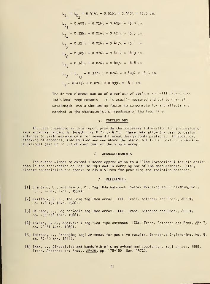
L = L = .41 ^tX + 0.026A = 0.440A = 16.0 cm.
1 2
L = 0.409A + 0.026A = 0.435A = 15-8 cm.
L n= 0.395A + 0.026A = .421 X = 15-3 cm.
U4
Ln
= 0. 391 X + 0.026A = 0.417A = 15.1 cm.
5
L = 0.385X + 0.026A = 0.41 IX = 14.9 cm.D6
L = 0.381A + 0.026A = 0.407A = 14.8 cm.
7
L - L = 0.377A + 0.026A = 0.403A = 14.6 cm.D8
D13
L D= 0.473A + 0.026A = 0.499A = 18.1 cm.
R
The driven element can be of a variety of designs and will depend upon
individual requirements. It is usually measured and cut to one-half
wavelength less a shortening factor to compensate for end-effects and
matched to the characteristic impedance of the feed line.
5. CONCLUSIONS
The data presented in this report provide the necessary information for the design ofYagi antennas ranging in length from 0.2A to 4.2A. These data allow the user to designantennas to yield maximum gain for seven different design configurations. In addition,stacking of antennas, side by side and one above the othei
—
all fed in phase—provides an
additional gain up to 5.2 dB over that of the single array.
6. ACKNOWLEDGMENTS
The author wishes to extend sincere appreciation to William Gorboczieski for his assist-ance in the fabrication of test set-ups and in carrying out of the measurements. Also,sincere appreciation and thanks to Alvin Wilson for providing the radiation patterns.
7. REFERENCES
[1] Shintaro, U., and Yasuto, M. , Yagi-Uda Antennas (Sasoki Printing and Publishing Co.,
Ltd., Senda, Japan, 1954).
[2] Mailloux, R. J., The long Yagi-Uda array, IEEE, Trans. Antennas and Prop., AP-1
4
,
pp. 128-137 (Mar. 1966).
[3] Barbano, N. , Log periodic Yagi-Uda array, IEEE, Trans. Antennas and Prop., AP-1
4
,
pp. 235-238 (Mar. 1966).
[4] Thiele, G. A., Analysis Y Yagi-Uda type antennas, IEEE, Trans. Antennas and Prop. AP-1
7
,
pp. 24-31 (Jan. 1 969)
.
[5] Emerson, J., Arranging Yagi antennas for positive results, Broadcast Engineering, No. 5,
pp. 32-40 (May 1971).
[6] Shen, L., Directivity and bandwidth of single-band and double band Yagi arrays, IEEE,
Trans. Antennas and Prop., AP-20, pp. 178-I8O (Nov. 1972).
21
[7] Cheng, D. K. , and Chen, C. A., Optimum element spacings for Yagi-Uda arrays, IEEE, TransAntennas and Prop., AP-21
, pp. 615-623 (Sept. 1973).
[8] Chen, C. A., and Cheng, D. K. , Optimum element lengths for Yagi-Uda arrays, IEEE, Trans.Antennas and Prop., AP-23
, pp. 8-15 (Jan. 1975).
[9] Nose, K. , Crossed Yagi antennas for circular polarization, QST, pp. 21-24 (Jan. 1973).
[10] Healey, D. J., Ill, An examination of the Gamma Match, QST, pp. 11-15 (Apr. 1969).
[11] Nose, K. , Adjustment of Gamma-matched parasitic beams, QST, pp. kk-hS (Mar. 1958).
[12] The Radio Amateur's Handbook, Fifty Second Ed. (AM Radio Relay League, 1976).
22

m^mi^^U.S. DEPT. OF COMM.
Er.BLIOGRAPHIC DATASHEET
1. PUBLICATION OR REPORT NO.
NBS-TN-688
2. Gov't AccessionNo.
4. TITLE AND SUBTITLE
YAGI ANTENNA DESIGN
3. Recipient's Accession No.
5. Publication Date
December 1976
6. Performing Organization Code
277.00
7. AUTHOR(S)Peter P. Viezbicke
8. Performing Organ. Report No.
9. PERFORMING ORGANIZATION NAME AND ADDRESS
NATIONAL BUREAU OF STANDARDSDEPARTMENT OF COMMERCEWASHINGTON, D.C. 20234
10. Project/Task/Work Unit No.
2776124
11. Contract/Grant No.
12. Sponsoring Organization Name and Complete Address (Street, City, State, ZIP)
Same as 9.
13. Type of Report & PeriodCovered
FINAL14. Sponsoring Agency Code
15. SUPPLEMENTARY NOTES
16. ABSTRACT (A 200-word or less factual summary of most significant information. If document includes a significant
bibliography or literature survey, mention it here.)
This report presents data, using modeling techniques, for the optimum design ofdifferent length Yagi antennas. This information is presented in graphical form tofacilitate the design of practical length antennas--from 0.2A to 4.2A long--foroperation in the HF, VHF, and UHF frequency range. The effects of differentantenna parameters on realizable gain were also investigated and the results arepresented. Finally, supplemental data are presented on the stacking of two or moreantennas to provide additional gain.
17. KEY WORDS (six to twelve entries; alphabetical order; capitalize only the first letter of the first key word unless a proper
name; separated by semicolons)
Antenna, director, driven element, gain, radiation pattern, reflector, Yagi.
18. AVAILABILITY IXX Unlimited
~2 For Official Distribution. Do Not Release to NTIS
)CX! Order From Sup. of Doc, U.S. Government Pruitine OfficeWashington, D.C. 20402, SD Cat. No. C13 -46 ! 688
J Order From National Technical Information Service (NTIS)Springfield, Virginia 22151
19. SECURITY CLASS(THIS REPORT)
UNCLASSIFIED
20. SECURITY CLASS(THIS PAGE)
UNCLASSIFIED
21. NO. OF PAGES
27
22. Price
$0.65


NBS TECHNICAL PUBLICATIONS
PERIODICALS
JOURNAL OF RESEARCH reports National Bureauof Standards research and development in physics,
mathematics, and chemistry. It is published in twosections, available separately:
• Physics and Chemistry (Section A)Papers of interest primarily to scientists working in
these fields. This section covers a broad range of physi-
cal and chemical research, with major emphasis onstandards of physical measurement, fundamental con-
stants, and properties of matter. Issued six times a year.
Annual subscription: Domestic, $17.00; Foreign, $21.25.
• Mathematical Sciences (Section B)Studies and compilations designed mainly for the math-ematician and theoretical physicist. Topics in mathemat-ical statistics, theory of experiment design, numericalanalysis, theoretical physics and chemistry, logical de-
sign and programming of computers and computer sys-
tems. Short numerical tables. Issued quarterly. Annualsubscription: Domestic, $9.00; Foreign, $11.25.
DIMENSIONS/NBS (formerly Technical News Bulle-
tin)—This monthly magazine is published to informscientists, engineers, businessmen, industry, teachers,
students, and consumers of the latest advances in
science and technology, with primary emphasis on thework at NBS. The magazine highlights and reviewssuch issues as energy research, fire protection, building
technology, metric conversion, pollution abatement,health and safety, and consumer product performance.In addition, it reports the results of Bureau programsin measurement standards and techniques, properties of
matter and materials, engineering standards and serv-
ices, instrumentation, and automatic data processing.
Annual subscription: Domestic, $9.45; Foreign, $11.85.
NONPERIODICALS
Monographs—Major contributions to the technical liter-
ature on various subjects related to the Bureau's scien-
tific and technical activities.
Handbooks—Recommended codes of engineering andindustrial practice (including safety codes) developed
in cooperation with interested industries, professional
organizations, and regulatory bodies.
Special Publications—Include proceedings of conferences
sponsored by NBS, NBS annual reports, and other
special publications appropriate to this grouping suchas wall charts, pocket cards, and bibliographies.
Applied Mathematics Series—Mathematical tables, man-uals, and studies of special interest to physicists, engi-
neers, chemists, biologists, mathematicians, com-puter programmers, and others engaged in scientific
and technical work.
National Standard Reference Data Series—Providesquantitative data on the physical and chemical proper-
ties of materials, compiled from the world's literature
and critically evaluated. Developed under a world-wideprogram coordinated by NBS. Program under authority
of National Standard Data Act (Public Law 90-396).
NOTE: At present the principal publication outlet for
these data is the Journal of Physical and ChemicalReference Data (JPCRD) published quarterly for NBSby the American Chemical Society (ACS) and the Amer-ican Institute of Physics (AIP). Subscriptions, reprints,
and supplements available from ACS, 1155 Sixteenth
St. N.W., Wash. D. C. 20056.
Building Science Series—Disseminates technical infor-
mation developed at the Bureau on building materials,
components, systems, and whole structures. The series
presents research results, test methods, and perform-ance criteria related to the structural and environmentalfunctions and the durability and safety characteristics
of building elements and systems.
Technical Notes—Studies or reports which are completein themselves but restrictive in their treatment of asubject. Analogous to monographs but not so compre-hensive in scope or definitive in treatment of the sub-
ject area. Often serve as a vehicle for final reports of
work performed at NBS under the sponsorship of othergovernment agencies.
Voluntary Product Standards—Developed under proce-
dures published by the Department of Commerce in Part10, Title 15, of the Code of Federal Regulations. Thepurpose of the standards is to establish nationally rec-
ognized requirements for products, and to provide all
concerned interests with a basis for common under-standing of the characteristics of the products. NBSadministers this program as a supplement to the activi-
ties of the private sector standardizing organizations.
Consumer Information Series—Practical information,based on NBS research and experience, covering areasof interest to the consumer. Easily understandable lang-
uage and illustrations provide useful background knowl-edge for shopping in today's technological marketplace.
Order above NBS publications from: Superintendentof Documents, Government Printing Office, Washington,D.C. 20402.
Order following NBS publications—NBSIR's and FIPSfrom the National Technical Information Services,
Springfield, Va. 22161.
Federal Information Processing Standards Publications(FIPS PUBS)—Publications in this series collectively
constitute the Federal Information Processing Stand-ards Register. Register serves as the official source of
information in the Federal Government regarding stand-ards issued by NBS pursuant to the Federal Propertyand Administrative Services Act of 1949 as amended,Public Law 89-306 (79 Stat. 1127), and as implementedby Executive Order 11717 (38 FR 12315, dated May 11,
1973) and Part 6 of Title 15 CFR (Code of FederalRegulations).
NBS Interagency Reports (NBSIR)—A special series of
interim or final reports on work performed by NBS for
outside sponsors (both government and non-govern-ment). In general, initial distribution is handled by the
sponsor; public distribution is by the National Techni-cal Information Services (Springfield, Va. 22161) in
paper copy or microfiche form.
BIBLIOGRAPHIC SUBSCRIPTION SERVICESThe following current-awareness and literature-survey
bibliographies are issued periodically by the Bureau:Cryogenic Data Center Current Awareness Service. A
literature survey issued biweekly. Annual subscrip-
tion: Domestic, $20.00; Foreign, $25.00.
Liquified Natural Gas. A literature survey issued quar-
terly. Annual subscription: $20.00.
Superconducting Devices and Materials. A literature
survey issued quarterly. Annual subscription: $20.00.
Send subscription orders and remittances for the pre-
ceding bibliographic services to National Bureau of
Standards, Cryogenic Data Center (275.02) Boulder,
Colorado 80302.

U.S. DEPARTMENT OF COMMERCENational Bureau of StandardsWashington. DC. 20234
OFFICIAL BUSINESS
Penalty for Private Use. $300
POSTAGE AND FEES PAID
U.S. DEPARTMENT OF COMMERCECOM-21 5
Fourth Class Mail
jO^'OA,.
'^6-l9lfe
*7e> YEARS
1901-1976