Embed Size (px)
DESCRIPTION
sub
Citation preview
SW10
1
CONTENTS
SPECIFICATIONS ................................................. 3DIMENSIONS ............................................................ 3PANEL LAYOUT ..................................... 4CIRCUIT BOARD LAYOUT ................. 4BLOCK DIAGRAM ................................ 4DISASSEMBLY PROCEDURE ............................. 5CIRCUIT BOARD ........................................... 6INSPECTIONS ......................................................... 8/10OVERALL CIRCUIT DIAGRAMPARTS LIST
SERVICE MANUAL
PA 011489
20000125-85000 0.29K-5531 Printed in Japan ’99.12
HAMAMATSU, JAPAN
SW10
SW10
2
IMPOR TANT NOTICE
This manual has been provided for the use of authorized Yamaha Retailers and their service personnel. It has been assumedthat basic service procedures inherent to the industry, and ÏWre specifically Yamaha Products, are already known and under-stood by the users, and have therefore not been restated.
WARNING : Failure to follow appropriate service and safety procedures when servicing this product may result in per-sonal injury, destruction of expensive components and failure of the product to perform as specified. Forthese reasons, we advise all Yamaha product owners that all service required should be performed by anauthorized Yamaha Retailer or the appointed service repr esentative.
IMPORTANT : This presentation or sale of this manual to any individual or firm does not constitute authorization certifi-cation, recognition of any applicable technical capabilities, or establish a principal-agent relationship ofany form.
The data provided is belived to be accurate and applicable to the unit(s) indicated on the cover. The research engineering, andservice departments of Yamaha are continually striving to improve Yamaha products. Modifications are, therefore, inevitableand changes in specification are subject to change without notice or obligation to retrofit. Should any discrepancy appear toexist, please contact the distributor’s Service Division.
WARNING : Static discharges can destroy expensive components. Discharge any static electricity your body may haveaccumulated by grounding yourself to the ground buss in the unit (heavy gauge black wires connect tothis buss.)
IMPORTANT : Turn the unit OFF during disassembly and parts replacement. Recheck all work before you apply powerto the unit.
WARNING: CHEMICAL CONTENT NOTICE!
The solder used in the produc tion of this product contains LEAD. In addition, other electrical/electronic and/or plastic (Whereapplicable) components may also contain traces of chemicals found by the California Health and Welfare Agency (and possiblyother entities) to cause cancer and/or birth defects or other reproductive harm.
DO NOT PLACE SOLDER, ELECTRICAL/ELECTRONIC OR PLASTIC COMPONENTS IN YOUR MOUTH FOR ANY REASON WHATSO EVER!
Avoid prolonged, unprotected contact between solder and your skin! When soldering, do not inhale solder fumes or exposeeyes to solder/flux vapor!
If you come in contact with solder or components located inside the enclosure of this product, wash your hands before handlingfood.
WARNING
Components having special characteristics are marked and must be replaced with parts having specification equal to thoseoriginally installed.
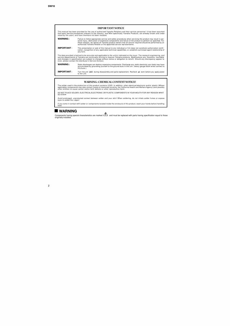
General specificationsType...........................................Bass Reflex Powered SpeakerFrequency Range .......................25–150 Hz (–10 dB)Sensitivity .................................. –12 dB at Vol. Max (for 100 dB/SPL, 1 m on Axis)Maximum Output Level .............111 dB (1 m on Axis)Dimensiones (W × H × D)..........328 × 459 × 476 mmWeight.......................................26 kg
Speaker unitSpeaker Unit..............................25 cm Cone (8Ω, magnetic shielded)Enclosure...................................Type: Bass Reflex
Amp.unitMaximum Output Power............180 W at 100 Hz, THD= 1%, RL= 8ΩInput Sensitivity/Impedance....... –6 dB to +4 dB/10 kΩ (Input 1, 2, 3)Hum & Noise.............................≤–60 dBu (Volume= Min) DIN Audio filterSignal to Noise Ratio..................≥100 dB (IEC-A Weighting)Controls .....................................VOL (Level Control)
CUTOFF FREQ. Control: 40–120 Hz (Variable)PHASE Switch: REV/NORMPOWER Switch: ON/OFF
Connectors ............................... Input 1, 2, 3 (XLR-3-31), Output 1, 2, 3 (XLR-3-32)Power Indicator/Clip Indicator ... Green/Red LEDPower Requirement....................USA and Canada: AC 120 V, 60 Hz
Europe: AC 230 V, 50 HzOthers: AC 240 V, 50 Hz
Power Consumption...................160 W
W: 328
H : 4 5 9
407
D: 476
SPECIFICATIONS
DIMENSIONS
4
SW10
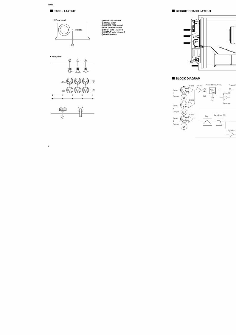
PANEL LAYOUT CIRCUIT BOARD LAYOUT
BLOCK DIAGRAM
VOL
MIN MAX
CUTOFF FREQ.
INPUT
(–6dB~+4dB)
OUTPUT
(THRU)
80
1 2 3
40 120REVPHASE
NORM
POWER
ON OFF
1
2 3 4
5
6
7
MAIN 4/5
MAIN 3/5
MAIN 2/5
MAIN 1/5
Input
IC101
IC102
IC102
IC101
1 6 72
3
76
5
12
3
IC1041
Output
Input
2
Output
Input
3
Output
Vol.
Cutoff Freq. Cont.
Low Pass FIL.
Phase SW.
Inverter
Inverter
EQ
N
R
1
2
3
4
5
6
7
Power/Clip indicator
PHASE switch
CUTOFF FREQ control
VOL (Volume) control
INPUT jacks 1, 2, and 3
OUTPUT jacks 1, 2, and 3
POWER switch
Front panel
Rear panel
DISASSEMBLY PROCEDURE
Fig.1
Fig.3
1. Woofer
1-1 Remove the front grille.
1-2. Remove the eight (8) screws marked [140]. The
woofer can then be removed. (Fig.1)
2. Control Panel
2-1 Remove the four (4) screws marked [170]. The
control panel can then be removed. (Fig.2)
3. Rear Panel
3-1 Remove the six (6) screws marked [100]. The rear
panel can then be removed. (Fig.2)
4. Power Transformer
4-1 Remove the rear panel. (See procedure 3.)
4-2 Remove the four (4) screws marked [160]. The power
transformer can then be removed. (Fig.3)
5. MAIN 1/5 Circuit Board
5-1 Remove the Control Panel. (See procedure 2.)
5-2 Remove the twelve (12) screws marked [130]. The
MAIN 1/5 circuit board can then be removed.(Fig.2)
6. MAIN 2/5 Circuit Board
6-1 Remove the control panel. (See procedure 2.)
6-2 Remove the rear panel. (See procedure 3.)
6-3 Remove the MAIN 2/5 circuit board from spacer
support. (Fig.3)
7. MAIN 3/5 Circuit Board
7-1 Remove the MAIN 2/5 circuit board. (See procedure 6.)
7-2 Remove the eight (8) screws marked [150]. The TR
press metal A marked [A90 and the TR press metal
B marked [A100] can then be removed.
7-3 Remove the four (4) screws marked [140A]. The
MAIN 3/5 circuit board can then be removed. (Fig.3)
8. MAIN 4/5 Circuit Board
8-1 Remove the rear panel. (See procedure 3.)
8-2 Remove the two (2) screws marked [140B]. The
MAIN 4/5 circuit board can then be removed. (Fig.3)
9. MAIN 5/5 Circuit Board
9-1 Remove the front panel.
9-2 Remove the two (2) screws marked [110]. The MAIN
5/5 circuit board can then be removed. (Fig.4)
[110]
[140]
[140][130]
[100]
[140A]
[160]
[140B]
[160]
[150]
[140A]
[140]
[150]
Spacer Support
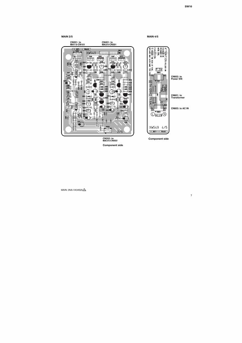
MAIN 2/5
MAIN 3/5
CN101: toMA2/5-CN201
CUTOFFFREQ.
VOL.
INPUT OUTPUT
1
2
3
PHASE
6
SW10
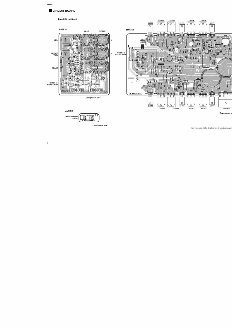
CIRCUIT BOARD
MAIN Circuit Board
Component side
CN301: toMA2/5-CN401
CN604: to MA3/5-CN501
Component side
Component side
MAIN 1/5 MAIN 3/5
MAIN 5/5
Note : See parts list for details of circuit board component parts.
SW10
7
CN201: to
MA1/5-CN101
CN401: to
MA3/5-CN301
CN202: to
MA3/5-CN502
CN602: to
Power SW.
CN601: to
Transformer
CN603: to AC IN
Component side
MAIN: 3NA-V434520 2
MAIN 2/5
Component side
MAIN 4/5
SW10
8
INSPECTIONS
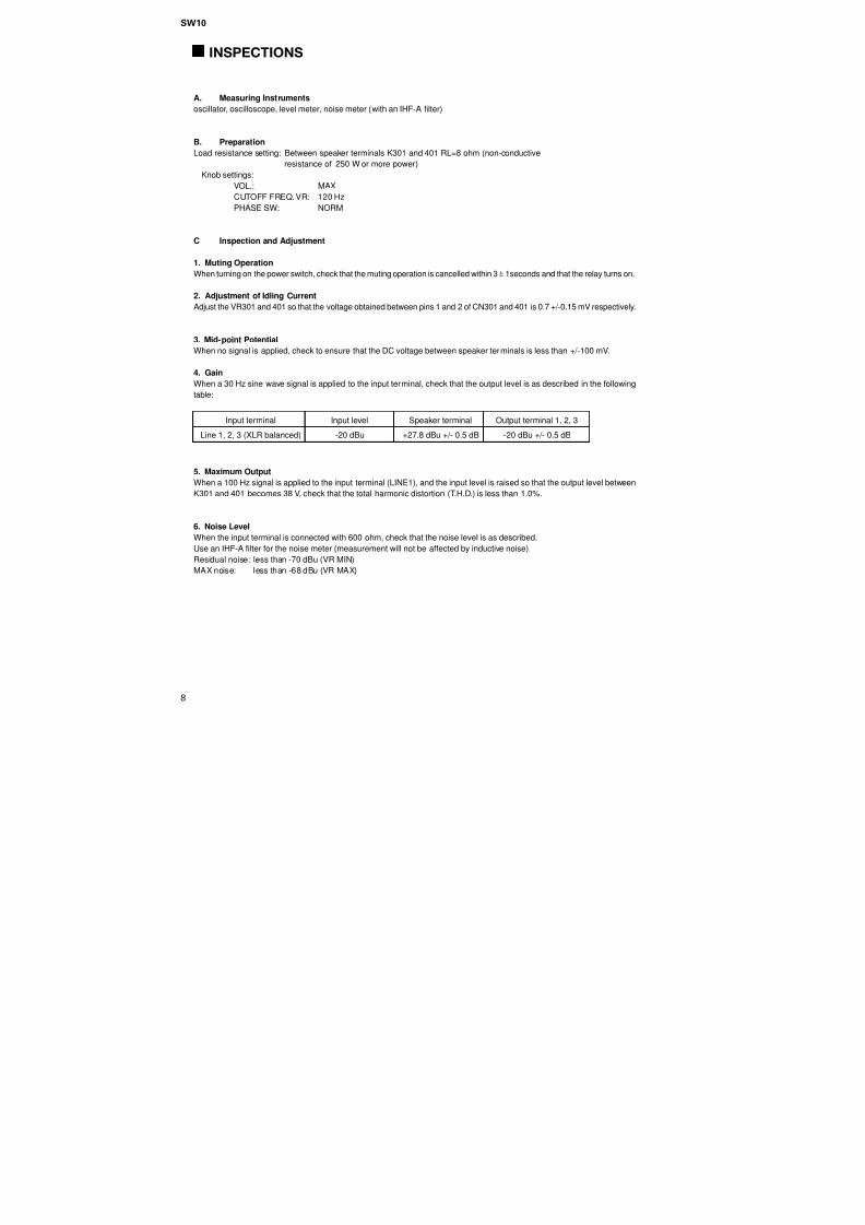
A. Measuring Instruments
oscillator, oscilloscope, level meter, noise meter (with an IHF-A filter)
B. Preparation
Load resistance setting: Between speaker terminals K301 and 401 RL=8 ohm (non-conductiveresistance of 250 W or more power)
Knob settings:VOL.: MAXCUTOFF FREQ. VR: 120 HzPHASE SW: NORM
C Inspection and Adjustment
1. Muting Operation
When turning on the power switch, check that the muting operation is cancelled within 3± 1seconds and that the relay turns on.
2. Adjustment of Idling Current
Adjust the VR301 and 401 so that the voltage obtained between pins 1 and 2 of CN301 and 401 is 0.7 +/-0.15 mV respectively.
3. Mid-point Potential
When no signal is applied, check to ensure that the DC voltage between speaker terminals is less than +/-100 mV.
4. Gain
When a 30 Hz sine wave signal is applied to the input terminal, check that the output level is as described in the followingtable:
5. Maximum Output
When a 100 Hz signal is applied to the input terminal (LINE1), and the input level is raised so that the output level betweenK301 and 401 becomes 38 V, check that the total harmonic distortion (T.H.D.) is less than 1.0%.
6. Noise Level
When the input terminal is connected with 600 ohm, check that the noise level is as described.Use an IHF-A filter for the noise meter (measurement will not be affected by inductive noise).Residual noise: less than -70 dBu (VR MIN)MAX noise: less than -68 dBu (VR MAX)
Input terminal Input level Speaker terminal Output terminal 1, 2, 3
Line 1, 2, 3 (XLR balanced) -20 dBu +27.8 dBu +/- 0.5 dB -20 dBu +/- 0.5 dB
SW10
9
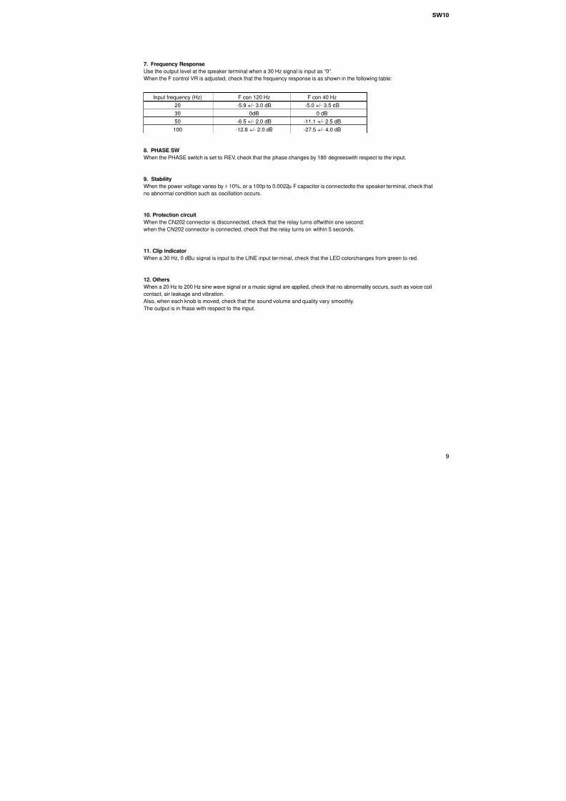
7. Frequency Response
Use the output level at the speaker terminal when a 30 Hz signal is input as “0”.When the F control VR is adjusted, check that the frequency response is as shown in the following table:
8. PHASE SW
When the PHASE switch is set to REV, check that the phase changes by 180 degreeswith respect to the input.
9. Stability
When the power voltage varies by ± 10%, or a 100p to 0.0022µ F capacitor is connectedto the speaker terminal, check thatno abnormal condition such as oscillation occurs.
10. Protection circuit
When the CN202 connector is disconnected, check that the relay turns offwithin one second;when the CN202 connector is connected, check that the relay turns on within 5 seconds.
11. Clip indicator
When a 30 Hz, 0 dBu signal is input to the LINE input terminal, check that the LED colorchanges from green to red.
12. Others
When a 20 Hz to 200 Hz sine wave signal or a music signal are applied, check that no abnormality occurs, such as voice coilcontact, air leakage and vibration.Also, when each knob is moved, check that the sound volume and quality vary smoothly.The output is in fhase with respect to the input.
Input frequency (Hz) F con 120 Hz F con 40 Hz
20 -5.9 +/- 3.0 dB -5.0 +/- 3.5 dB
30 0dB 0 dB
50 -6.5 +/- 2.0 dB -11.1 +/- 2.5 dB
100 -12.8 +/- 2.0 dB -27.5 +/- 4.0 dB

SW10
10

SW10
11
PARTS LISTCONTENTS
OVERALL ASSEMBLY ............................................. 2ELECTRICAL PARTS ............................................ 4
SW10
WARNINGComponents having special characteristics are marked and must be replaced with parts havingspecification equal to those originally installed.
Notes : DESTINATION ABBREVIATIONS
The numbers “QTY” show quantities for each unit.The parts with “--” in “PART NO.” are not available as spare parts.This mark “ ” in the REMARKS column means these parts are interchangeable.The second letter of the shaded ( ) part number is O, not zero.The second letter of the shaded ( ) part number is I, not one.
M: South African modelO : Chinese modelQ : South-east Asia modelT : Taiwan modelU : U.S.A. modelV : General export model (110V)W: General export model (220)N,X : General export modelY : Export model
A : Australian modelB : British modelC : Canadian modelD : German modelE : European modelF : French modelH : North European modelI : Indonesian modelJ : Japanese model
SW10
2
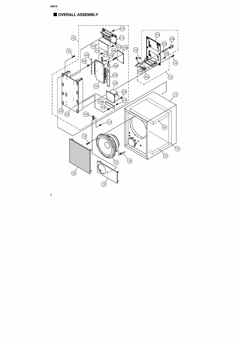
OVERALL ASSEMBLY
130
A30
A10
110
140
80
20
70
60
60
90
30
10
50
A140
A160
A170
A110
A130
A120
A50d
A50e
A50a
100
150
R80
R30
R40
R50
R10
40R80a
A80
A70
A60
A90
A40
A20
A150
A140
A100
A50c
A50b
SW10
3
*
*
*
*
*
*
*
*
*
*
*
*
*
*
*
*
*
*
*
*
*
*
*
New Parts
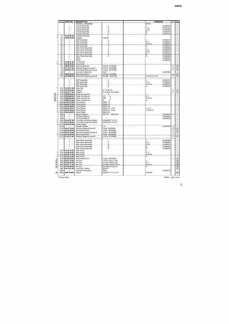
REF NO. PART NO. DESCRIPTION REMARKS QTY RANK
RANK : Japan only
OVERALL ASSEMBLY SW10Overall Assembly J J (V436470)Overall Assembly U U, V (V436480)Overall Assembly H H, W (V436490)Overall Assembly B B (V436500)Overall Assembly A A (V436510)
10 Cabinet Assembly J20 Speaker 250mm30 AMP Assembly J J (V436570)30 AMP Assembly U U, V (V436630)30 AMP Assembly H H, W, B (V436640)30 AMP Assembly A A (V436650)40 Rear Panel Assembly J J (V436580)40 Rear Panel Assembly U U, V (V436660)40 Rear Panel Assembly H H, W (V436670)40 Rear Panel Assembly B B (V436680)40 Rear Panel Assembly A A (V436690)50 Felt A (V436590)60 Felt B (V436600)70 Front Panel80 Front Grille90 Bind Head Screw 5.0X30 MFZN2BL 8 01100 Bonding Tapping Screw-B 4.0X10 MFZN2BL 6 01110 Bind Head Tapping Screw-B 3.0X8 MFZN2BL 2 01130 Connector Assembly C&F (V435790)140 Bind Head Screw 4.0X25 MFZN2BL 8 01150 Bind Head Tapping Screw-B A4.0X8 MFZN2BL U, H, B, A, V, W 2 01
AMP Assembly J J (V436570)AMP Assembly U U, V (V436630)AMP Assembly H H, W, B (V436640)AMP Assembly A A (V436650)
A10 Heat SinkA20 Support H=7.4 B=5.5 4 01A30 Support H=15.0 B=7.0 M4/M3 2 01A40 Power Transformer A JA40 Power Transformer UC A U, VA40 Power Transformer CEE A H, W, BA40 Power Transformer A A AA50a Circuit Board MAIN 1/5A50b Circuit Board MAIN 2/5A50c Circuit Board MAIN 3/5A50d Circuit Board MAIN 4/5 J UC J, U, VA50d Circuit Board MAIN 4/5 H BA H, W, B, AA50e Circuit Board MAIN 5/5A60 Spacer Support KCA-20 PIN GOO (V434820) 4A70 TR Press Metal A (V434850)A80 TR Press Metal B (V434860)A90 Thermally Conductive Sheet UNISHEET T=0.15A100 Thermally Conductive Sheet UNISHEET T=0.15A110 Control PanelA120 Stopper Rubber CR (V435040) 8A130 Bonding Tapping Screw-B 3.0X8 MFZN2BL 12 01A140 Bind Head Screw 3.0X6 MFZN2BL 6 01A150 Bind Head Tapping Screw-B 3.0X12 MFZN2BL 9 01A160 Bind Head Screw 4.0X6 MFZN2BL 4A170 Bonding Tapping Screw-B 4.0X10 MFZN2BL 4 01
Rear Panel Assembly J J (V436580)Rear Panel Assembly U U, V (V436660)Rear Panel Assembly H H, W (V436670)Rear Panel Assembly B B (V436680)Rear Panel Assembly A A (V436690)
R10 Rear Panel JR10 Rear Panel U, VR10 Rear Panel H, W, BR10 Rear Panel AR30 Bind Head Screw 3.0X6 MFZN2BL 2 01R40 AC Cord J VCTF 2X0.75 12A J 05R40 AC Cord UC SJT 3X#18 10A U, V 06R40 AC Cord E H05VV-F3X0.7510A H, W, A 06R40 AC Cord BS H05VV-F3X0.75 B 08R50 Cord Strain Relief SR-6P1 01R80 Connector Assembly PSW (V434610)
R80a Switch SDDTA1-A-1 J.U.C.H POWER 06
--
--
--
--
--
V4 36 56 00
XW561A00
--
--
--
--
--
--
--
--
--
--
--
V4 36 61 00
V4 36 62 00
VB 66 45 00
VJ 25 41 00
EP600190
--
VB 92 32 00
VC 6888 00
--
--
--
--
V4 34 81 00
VV 08 65 00
V2 43 77 00
XW544A00
XW545A00
XW546A00
XW547A00
AAX08780
AAX08790
AAX08800
AAX08810
AAX08820
AAX08830
--
--
--
V4 34 87 00
V4 34 88 00
V4 36 70 00
--
VN 4133 00
EG330360
VQ074600
V4 34 90 00
VJ 25 41 00
--
--
--
--
--
V4 36 75 00
V4 36 76 00
V4 36 77 00
V4 36 78 00
EG330360
V3 27 70 00
VV 20 56 00
V3 27 71 00
VV 05 83 00
VV 10 31 00
--
VM744600
SW10
4
New Parts
*
*
*
*
*
*
*
*
*
*
*
*
*
*
*
*
*
ELECTRICAL PARTS
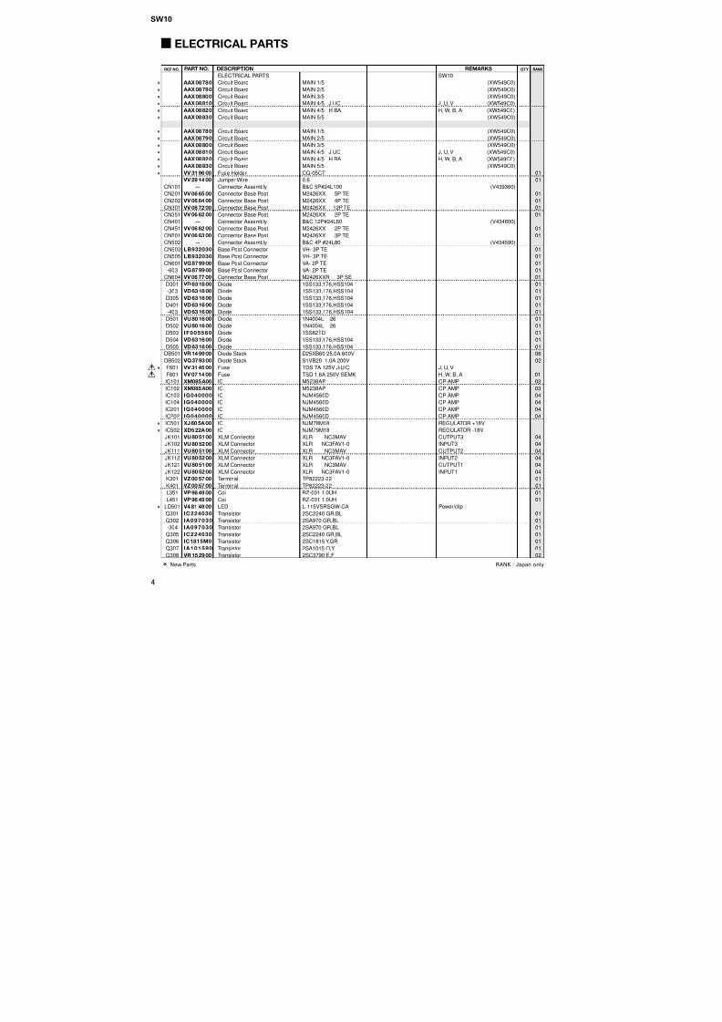
REF NO. PART NO. DESCRIPTION REMARKS QTY RANK
RANK : Japan only
ELECTRICAL PARTS SW10Circuit Board MAIN 1/5 (XW549C0)Circuit Board MAIN 2/5 (XW549C0)Circuit Board MAIN 3/5 (XW549C0)Circuit Board MAIN 4/5 J UC J, U, V (XW549C0)Circuit Board MAIN 4/5 H BA H, W, B, A (XW549C0)Circuit Board MAIN 5/5 (XW549C0)
Circuit Board MAIN 1/5 (XW549C0)Circuit Board MAIN 2/5 (XW549C0)Circuit Board MAIN 3/5 (XW549C0)Circuit Board MAIN 4/5 J UC J, U, V (XW549C0)Circuit Board MAIN 4/5 H BA H, W, B, A (XW549C0)Circuit Board MAIN 5/5 (XW549C0)Fuse Holder CQ-05CT 01Jumper Wire 0.6 01
CN101 Connector Assembly B&C 5P#24L100 (V439360)CN201 Connector Base Post M2426XX 5P TE 01CN202 Connector Base Post M2426XX 4P TE 01CN301 Connector Base Post M2426XX 12P TE 01CN351 Connector Base Post M2426XX 2P TE 01CN401 Connector Assembly B&C 12P#24L60 (V434600)CN451 Connector Base Post M2426XX 2P TE 01CN501 Connector Base Post M2426XX 3P TE 01CN502 Connector Assembly B&C 4P #24L80 (V434590)CN503 Base Post Connector VH- 3P TE 01CN505 Base Post Connector VH- 3P TE 01CN601 Base Post Connector VA- 2P TE 01-603 Base Post Connector VA- 2P TE 01
CN604 Connector Base Post M2426XXR 3P SE 01D301 Diode 1SS133,176,HSS104 01-303 Diode 1SS133,176,HSS104 01D305 Diode 1SS133,176,HSS104 01D401 Diode 1SS133,176,HSS104 01-403 Diode 1SS133,176,HSS104 01D501 Diode 1N4004L 26 01D502 Diode 1N4004L 26 01D503 Diode 1SS82TD 01D504 Diode 1SS133,176,HSS104 01D505 Diode 1SS133,176,HSS104 01
DB501 Diode Stack D25XB60 25.0A 600V 06DB502 Diode Stack S1VB20 1.0A 200V 02F601 Fuse TDS 7A 125V J/U/C J, U, VF601 Fuse TSD 1.6A 250V SEMK H, W, B, A 01IC101 IC M5238AP OP AMP 03IC102 IC M5238AP OP AMP 03IC103 IC NJM4560D OP AMP 04IC104 IC NJM4560D OP AMP 04IC201 IC NJM4560D OP AMP 04IC202 IC NJM4560D OP AMP 04IC501 IC NJM78M18 REGULATOR +18VIC502 IC NJM79M18 REGULATOR -18VJK101 XLM Connector XLR NC3MAV OUTPUT3 04JK102 XLM Connector XLR NC3FAV1-0 INPUT3 04JK111 XLM Connector XLR NC3MAV OUTPUT2 04JK112 XLM Connector XLR NC3FAV1-0 INPUT2 04JK121 XLM Connector XLR NC3MAV OUTPUT1 04JK122 XLM Connector XLR NC3FAV1-0 INPUT1 04K301 Terminal TP82223-22 01K401 Terminal TP82223-22 01L351 Coil RZ-001 1.0UH 01L451 Coil RZ-001 1.0UH 01
LD501 LED L-115VSRSGW-CA Power/clipQ301 Transistor 2SC2240 GR,BL 01Q302 Transistor 2SA970 GR,BL 01-304 Transistor 2SA970 GR,BL 01Q305 Transistor 2SC2240 GR,BL 01Q306 Transistor 2SC1815 Y,GR 01Q307 Transistor 2SA1015 O,Y 01Q308 Transistor 2SC3790 E,F 02
AAX 08780
AAX 08790
AAX 08800
AAX 08810
AAX 08820
AAX 08830
AAX 08780
AAX 08790
AAX 08800
AAX 08810
AAX 08820
AAX 08830
VV 31 96 00
VV 29 14 00
--
VV 06 65 00
VV 06 64 00
VV 06 72 00
VV 06 62 00
--
VV 06 62 00
VV 06 63 00
--
LB932030
LB932030
VG8799 00
VG8799 00
VV 06 77 00
VD63 16 00
VD63 16 00
VD63 16 00
VD63 16 00
VD63 16 00
VU80 16 00
VU80 16 00
IF005560
VD63 16 00
VD63 16 00
VR14 99 00
VQ3793 00
VV 31 45 00
VV 07 14 00
XM085A00
XM085A00
IG040000
IG040000
IG040000
IG040000
XJ60 5A 00
XD522A 00
VU80 51 00
VU80 52 00
VU80 51 00
VU80 52 00
VU80 51 00
VU80 52 00
VZ 00 57 00
VZ 00 57 00
VP 96 49 00
VP 96 49 00
V4 81 49 00
IC224030
IA097030
IA097030
IC224030
IC1815M0
IA101590
VR15 29 00
SW10
5
New Parts
*
*
*
*
*
*
*
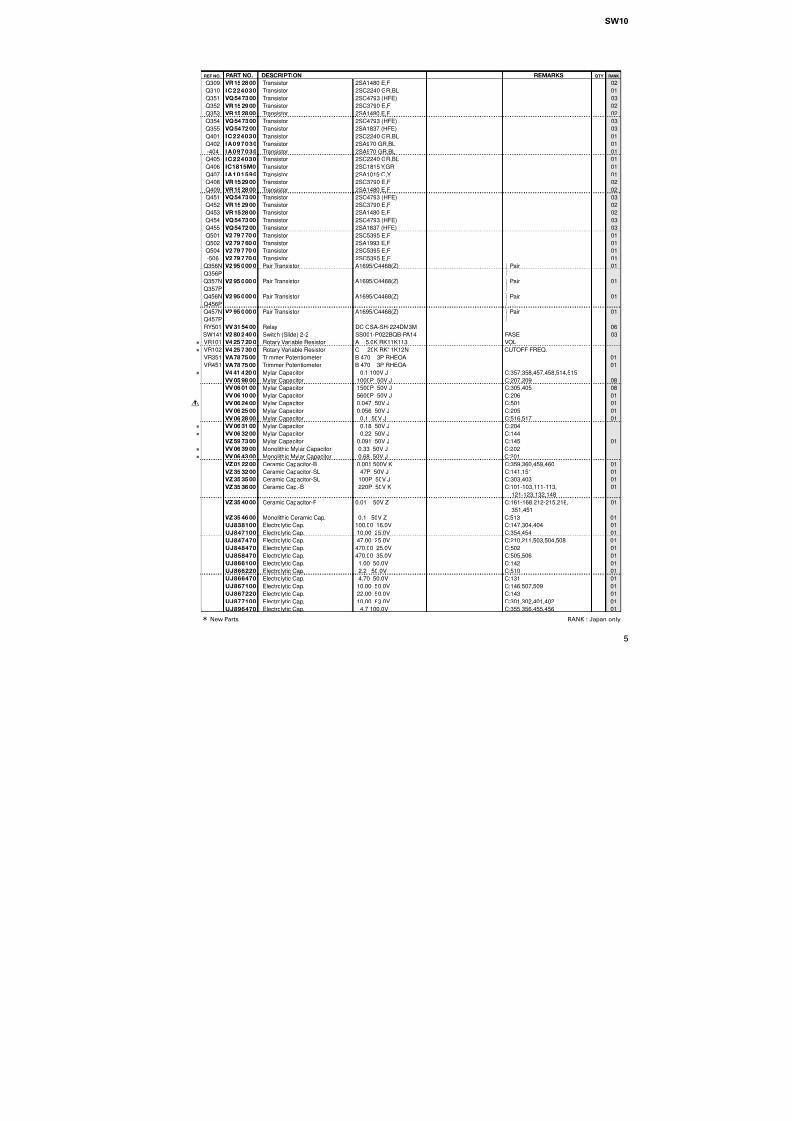
REF NO. PART NO. DESCRIPTION REMARKS QTY RANK
RANK : Japan only
Q309 Transistor 2SA1480 E,F 02Q310 Transistor 2SC2240 GR,BL 01Q351 Transistor 2SC4793 (HFE) 03Q352 Transistor 2SC3790 E,F 02Q353 Transistor 2SA1480 E,F 02Q354 Transistor 2SC4793 (HFE) 03Q355 Transistor 2SA1837 (HFE) 03Q401 Transistor 2SC2240 GR,BL 01Q402 Transistor 2SA970 GR,BL 01-404 Transistor 2SA970 GR,BL 01Q405 Transistor 2SC2240 GR,BL 01Q406 Transistor 2SC1815 Y,GR 01Q407 Transistor 2SA1015 O,Y 01Q408 Transistor 2SC3790 E,F 02Q409 Transistor 2SA1480 E,F 02Q451 Transistor 2SC4793 (HFE) 03Q452 Transistor 2SC3790 E,F 02Q453 Transistor 2SA1480 E,F 02Q454 Transistor 2SC4793 (HFE) 03Q455 Transistor 2SA1837 (HFE) 03Q501 Transistor 2SC5395 E,F 01Q502 Transistor 2SA1993 E,F 01Q504 Transistor 2SC5395 E,F 01-506 Transistor 2SC5395 E,F 01
Q356N Pair Transistor A1695/C4468(Z) Pair 01Q356PQ357N Pair Transistor A1695/C4468(Z) Pair 01Q357PQ456N Pair Transistor A1695/C4468(Z) Pair 01Q456PQ457N Pair Transistor A1695/C4468(Z) Pair 01Q457PRY501 Relay DC OSA-SH-224DM3M 06SW141 Switch (Slide) 2-2 SS001-P022BQB-PA14 FASE 03VR101 Rotary Variable Resistor A 5.0K RK11K113 VOLVR102 Rotary Variable Resistor C 20K RK11K12N CUTOFF FREQ.VR351 Trimmer Potentiometer B 470 3P RHEOA 01VR451 Trimmer Potentiometer B 470 3P RHEOA 01
Mylar Capacitor 0.1 100V J C:357,358,457,458,514,515Mylar Capacitor 1000P 50V J C:207,209 08Mylar Capacitor 1500P 50V J C:305,405 08Mylar Capacitor 5600P 50V J C:206 01Mylar Capacitor 0.047 50V J C:501 01Mylar Capacitor 0.056 50V J C:205 01Mylar Capacitor 0.1 50V J C:516,517 01Mylar Capacitor 0.18 50V J C:204Mylar Capacitor 0.22 50V J C:144Mylar Capacitor 0.091 50V J C:145 01Monolithic Mylar Capacitor 0.33 50V J C:202Monolithic Mylar Capacitor 0.68 50V J C:201Ceramic Capacitor-B 0.001 500V K C:359,360,459,460 01Ceramic Capacitor-SL 47P 50V J C:141,151 01Ceramic Capacitor-SL 100P 50V J C:303,403 01Ceramic Cap.-B 220P 50V K C:101-103,111-113, 01
121-123,132,148Ceramic Capacitor-F 0.01 50V Z C:161-168,212-215,216, 01
351,451Monolithic Ceramic Cap. 0.1 50V Z C:513 01Electrolytic Cap. 100.00 16.0V C:147,304,404 01Electrolytic Cap. 10.00 25.0V C:354,454 01Electrolytic Cap. 47.00 25.0V C:210,211,503,504,508 01Electrolytic Cap. 470.00 25.0V C:502 01Electrolytic Cap. 470.00 35.0V C:505,506 01Electrolytic Cap. 1.00 50.0V C:142 01Electrolytic Cap. 2.2 50.0V C:510 01Electrolytic Cap. 4.70 50.0V C:131 01Electrolytic Cap. 10.00 50.0V C:146,507,509 01Electrolytic Cap. 22.00 50.0V C:143 01Electrolytic Cap. 10.00 63.0V C:301,302,401,402 01Electrolytic Cap. 4.7 100.0V C:355,356,455,456 01
VR15 28 00
IC224030
VQ5473 00
VR15 29 00
VR15 28 00
VQ5473 00
VQ5472 00
IC224030
IA097030
IA097030
IC224030
IC1815M0
IA101590
VR15 29 00
VR15 28 00
VQ5473 00
VR15 29 00
VR15 28 00
VQ5473 00
VQ5472 00
V2 79 770 0
V2 79 760 0
V2 79 770 0
V2 79 770 0
V2 95 000 0
V2 95 000 0
V2 95 000 0
V2 95 000 0
VV 31 54 00
V2 80 240 0
V4 25 720 0
V4 25 730 0
VA78 75 00
VA78 75 00
V4 41 420 0
VV 05 98 00
VV 06 01 00
VV 06 10 00
VV 06 24 00
VV 06 25 00
VV 06 28 00
VV 06 31 00
VV 06 32 00
VZ 59 73 00
VV 06 39 00
VV 06 43 00
VZ 01 22 00
VZ 35 32 00
VZ 35 35 00
VZ 35 36 00
VZ 35 40 00
VZ 35 46 00
UJ838100
UJ847100
UJ847470
UJ848470
UJ858470
UJ866100
UJ866220
UJ866470
UJ867100
UJ867220
UJ877100
UJ896470
SW10
6
New Parts
*
*
*
*
*
*
*
*
*
*
*
*
*
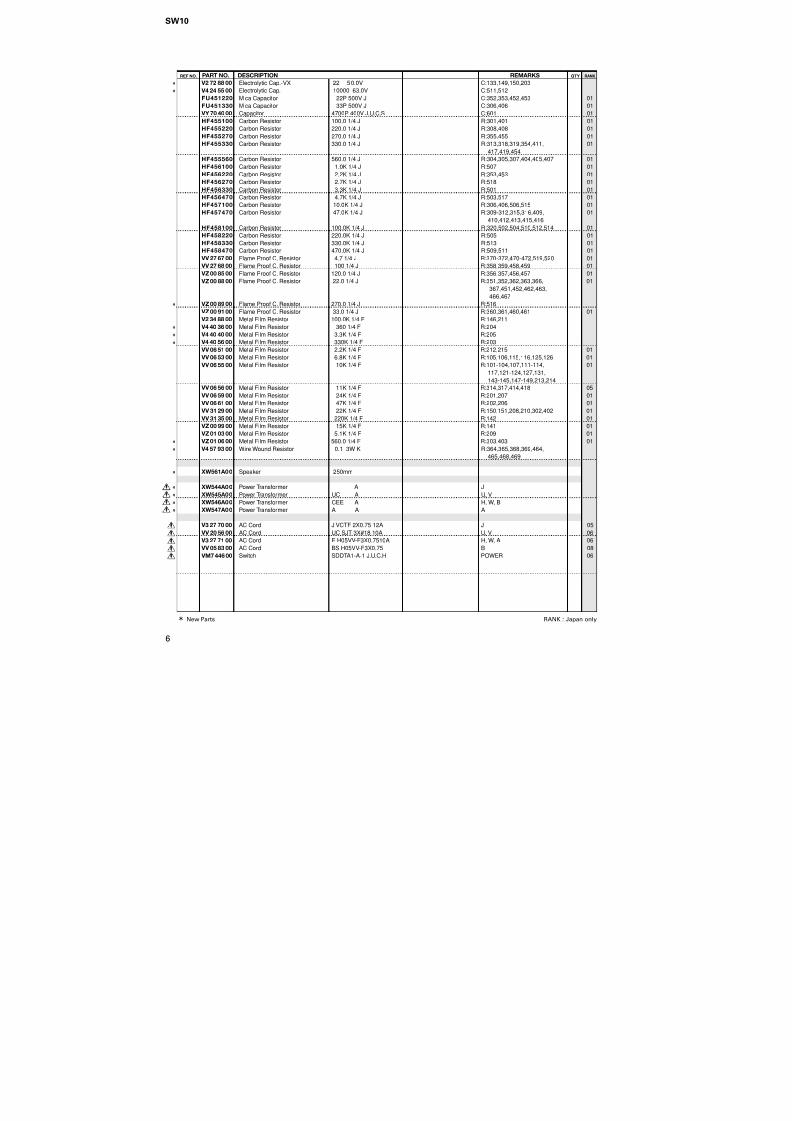
REF NO. PART NO. DESCRIPTION REMARKS QTY RANK
RANK : Japan only
Electrolytic Cap.-VX 22 50.0V C:133,149,150,203Electrolytic Cap. 10000 63.0V C:511,512Mica Capacitor 22P 500V J C:352,353,452,453 01Mica Capacitor 33P 500V J C:306,406 01Capacitor 4700P 400V J.U.C.S C:601 01Carbon Resistor 100.0 1/4 J R:301,401 01Carbon Resistor 220.0 1/4 J R:308,408 01Carbon Resistor 270.0 1/4 J R:355,455 01Carbon Resistor 330.0 1/4 J R:313,318,319,354,411, 01
417,419,454Carbon Resistor 560.0 1/4 J R:304,305,307,404,405,407 01Carbon Resistor 1.0K 1/4 J R:507 01Carbon Resistor 2.2K 1/4 J R:353,453 01Carbon Resistor 2.7K 1/4 J R:518 01Carbon Resistor 3.3K 1/4 J R:501 01Carbon Resistor 4.7K 1/4 J R:503,517 01Carbon Resistor 10.0K 1/4 J R:306,406,506,515 01Carbon Resistor 47.0K 1/4 J R:309-312,315,316,409, 01
410,412,413,415,416Carbon Resistor 100.0K 1/4 J R:320,502,504,510,512,514 01Carbon Resistor 220.0K 1/4 J R:505 01Carbon Resistor 330.0K 1/4 J R:513 01Carbon Resistor 470.0K 1/4 J R:509,511 01Flame Proof C. Resistor 4.7 1/4 J R:370-372,470-472,519,520 01Flame Proof C. Resistor 100 1/4 J R:358,359,458,459 01Flame Proof C. Resistor 120.0 1/4 J R:356,357,456,457 01Flame Proof C. Resistor 22.0 1/4 J R:351,352,362,363,366, 01
367,451,452,462,463,466,467
Flame Proof C. Resistor 270.0 1/4 J R:516Flame Proof C. Resistor 33.0 1/4 J R:360,361,460,461 01Metal Film Resistor 100.0K 1/4 F R:146,211Metal Film Resistor 360 1/4 F R:204Metal Film Resistor 3.3K 1/4 F R:205Metal Film Resistor 330K 1/4 F R:203Metal Film Resistor 2.2K 1/4 F R:212,215 01Metal Film Resistor 6.8K 1/4 F R:105,106,115,116,125,126 01Metal Film Resistor 10K 1/4 F R:101-104,107,111-114, 01
117,121-124,127,131,143-145,147-149,213,214
Metal Film Resistor 11K 1/4 F R:314,317,414,418 05Metal Film Resistor 24K 1/4 F R:201,207 01Metal Film Resistor 47K 1/4 F R:202,206 01Metal Film Resistor 22K 1/4 F R:150,151,208,210,302,402 01Metal Film Resistor 220K 1/4 F R:142 01Metal Film Resistor 15K 1/4 F R:141 01Metal Film Resistor 5.1K 1/4 F R:209 01Metal Film Resistor 560.0 1/4 F R:303,403 01Wire Wound Resistor 0.1 3W K R:364,365,368,369,464,
465,468,469
Speaker 250mm
Power Transformer A JPower Transformer UC A U, VPower Transformer CEE A H, W, BPower Transformer A A A
AC Cord J VCTF 2X0.75 12A J 05AC Cord UC SJT 3X#18 10A U, V 06AC Cord E H05VV-F3X0.7510A H, W, A 06AC Cord BS H05VV-F3X0.75 B 08Switch SDDTA1-A-1 J.U.C.H POWER 06
V2 72 88 00
V4 24 55 00
FU451220
FU451330
VY 70 40 00
HF455100
HF455220
HF455270
HF455330
HF455560
HF456100
HF456220
HF456270
HF456330
HF456470
HF457100
HF457470
HF458100
HF458220
HF458330
HF458470
VV 27 67 00
VV 27 68 00
VZ 00 85 00
VZ 00 88 00
VZ 00 89 00
VZ 00 91 00
V2 34 88 00
V4 40 36 00
V4 40 40 00
V4 40 56 00
VV 06 51 00
VV 06 53 00
VV 06 55 00
VV 06 56 00
VV 06 59 00
VV 06 61 00
VV 31 29 00
VV 31 35 00
VZ 00 99 00
VZ 01 03 00
VZ 01 06 00
V4 57 93 00
XW561A00
XW544A00
XW545A00
XW546A00
XW547A00
V3 27 70 00
VV 20 56 00
V3 27 71 00
VV 05 83 00
VM7446 00
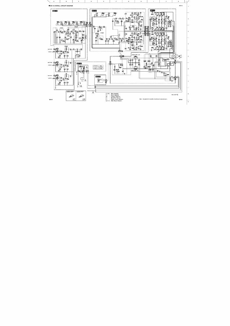
A CB D GFE JIH LK
9
8
7
6
5
4
3
2
1SW-10SW-10 OVERALL CIRCUIT DIAGRAM