Embed Size (px)
Citation preview
Pushing the resolution limits of photolithography: Understanding the fundamentals of the EUV resists
Yasin Ekinci Paul Scherrer Institute, SwitzerlandAdvanced Lithography and Metrology Group
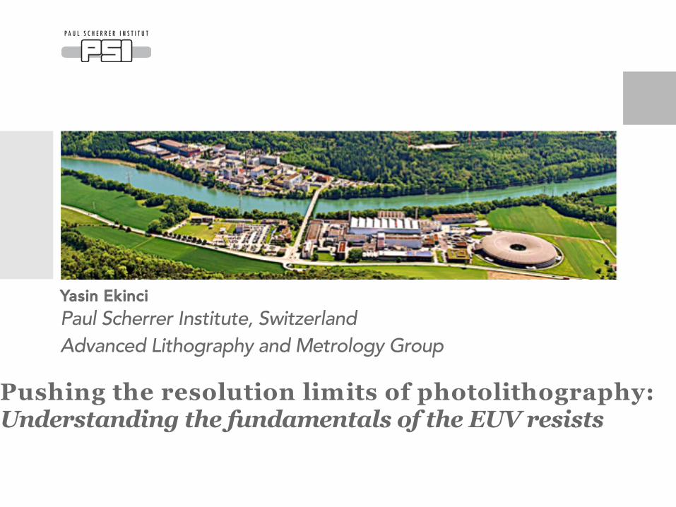
EUV Lithography
Page 2
9m3m
3m
n EUV lithography: n Reflective optics and maskn Plasma source
n EUV in high-volume production delayed mainly due to source power
n Planned for HVM production in 2017n Planned for HVM production in 2018
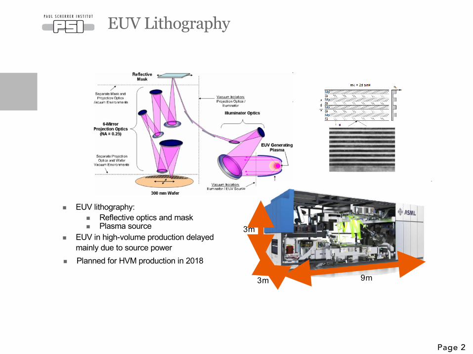
XIL-II: EUV-IL @ Swiss Light Source, PSI
Page 3
• Undulator source+ Switchable mirror+ pinhole- High brightness- High spatial coherence- 4% bandwidth- tunable wavelength (λ=2.5-18 nm)
• On-site cleanroom- Spin-coater, wet-bench, hot-plates, microscope,
developer, optical thickness measurement
EUV interference lithography
Quasi-crystals
D. Fan
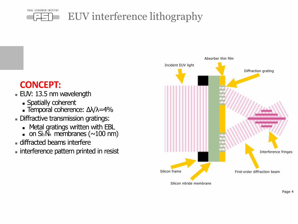
CONCEPT:n EUV: 13.5 nm wavelength
n Spatially coherent n Temporal coherence: Δλ/λ=4%
n Diffractive transmission gratings:n Metal gratings written with EBLn on Si3N4 membranes (~100 nm)
n diffracted beams interferen interference pattern printed in resist
Incident EUV light
Silicon nitride membrane
Diffraction grating
Absorber thin film
First-order diffraction beam
Interference fringes
Silicon frame
Page 4
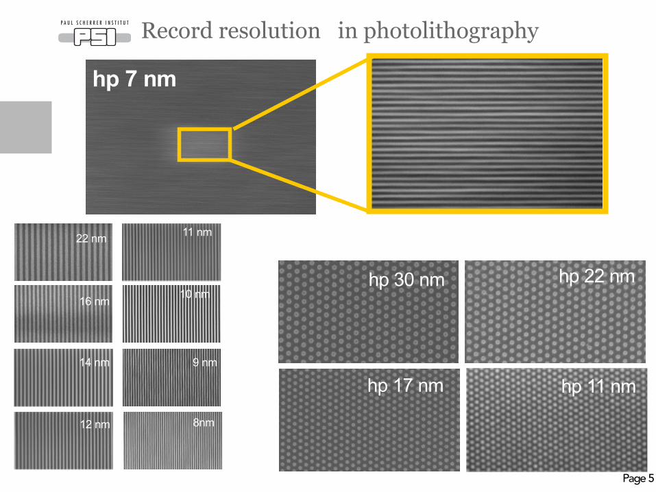
Record resolution in photolithography
22 nm
14 nm
16 nm
12 nm
10 nm
9 nm
11 nm
8nm
hp 7 nm
hp 30 nm hp 22 nm
hp 17 nm hp 11 nm
Page 5
Science with EUV-ILSi nanowires
• EUV resist development
• Nanoimprint stamps
• Fluidic confinement structures• Plasmonics and Metamaterials
• Polymer grafting
• Biomaterials
• Catalysis
• Templated assembly • Cell growth templates
• Nanomagnetism
• Fresnel Zone Plates
• etc.
Page 6
lw 20 nm
length ~1 µm
lw 6.5 nm
Si fins16 nm 11 nm
Height 88 nm
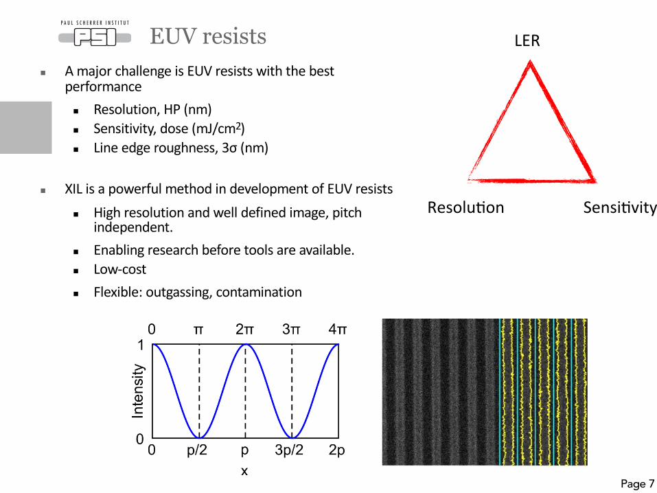
EUV resists LER
Resolu)on Sensi)vity
n A major challenge is EUV resists with the best performance
n Resolution, HP (nm)
n Sensitivity, dose (mJ/cm2)
n Line edge roughness, 3σ (nm)
n XIL is a powerful method in development of EUV resists
n High resolution and well defined image, pitch independent.
n Enabling research before tools are available.
n Low-cost
n Flexible: outgassing, contamination
Page 7
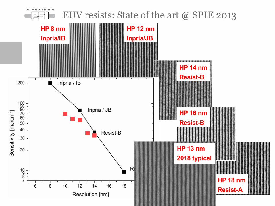
EUV resists: State of the art @ SPIE 2013
HP 14 nmResist-B
HP 16 nmResist-B
HP 18 nmResist-A
HP 12 nmInpria/JB
HP 8 nmInpria/IB
HP 13 nm2018 typical
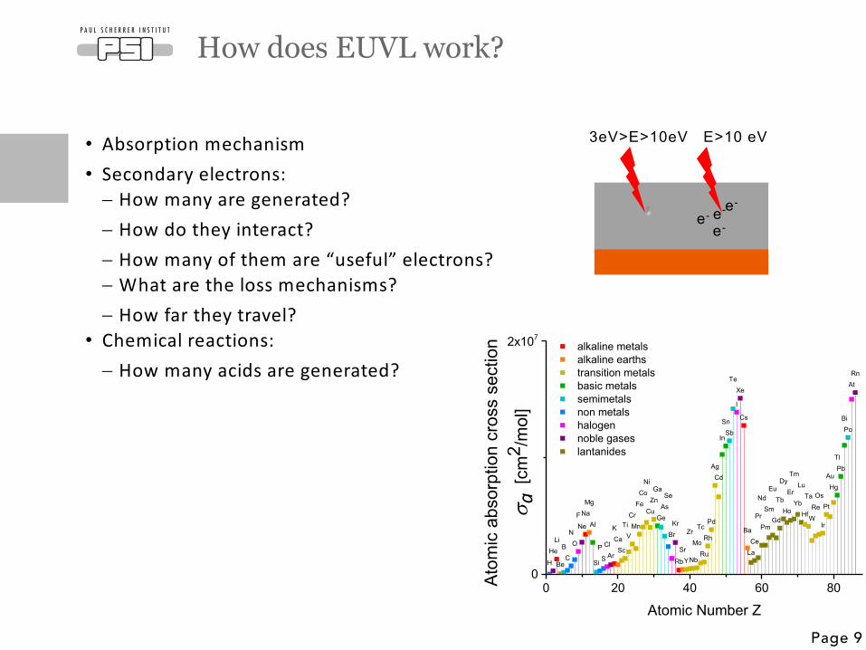
How does EUVL work?
• Absorption mechanism• Secondary electrons: - How many are generated?- How do they interact?- How many of them are “useful” electrons?- What are the loss mechanisms?- How far they travel?
• Chemical reactions:- How many acids are generated?
Page 9
e-
e-e-e-
3eV>E>10eV E>10 eV
0 20 40 60 800
2x10⁷
H
HeLi
Be
BC
NO
FNe
NaMg
Al
Si
PS
ClAr
KCa
Sc
TiV
CrMn
FeCo
Ni
CuZnGa
GeAsSe
BrKr
Rb
SrY
Zr
Nb
Mo
Tc
Ru
Rh
Pd
AgCd
In
SnSb
Te
I
Xe
Cs
Ba
LaCe
Pr
Nd
Pm
Sm
Eu
Gd
Tb
Dy
Ho
Er
Tm
Yb
Lu
Hf
Ta
WRe
Os
Ir
Pt
AuHg
TlPb
BiPo
AtRn
Atom
ic a
bsor
ptio
n cr
oss
sect
ion
s a [
cm2 /
mol
]
Atomic Number Z
Atomic absorption cross section at EUV (13.5 nm)
alkaline metals alkaline earths transition metals basic metals semimetals non metals halogen noble gases lantanides
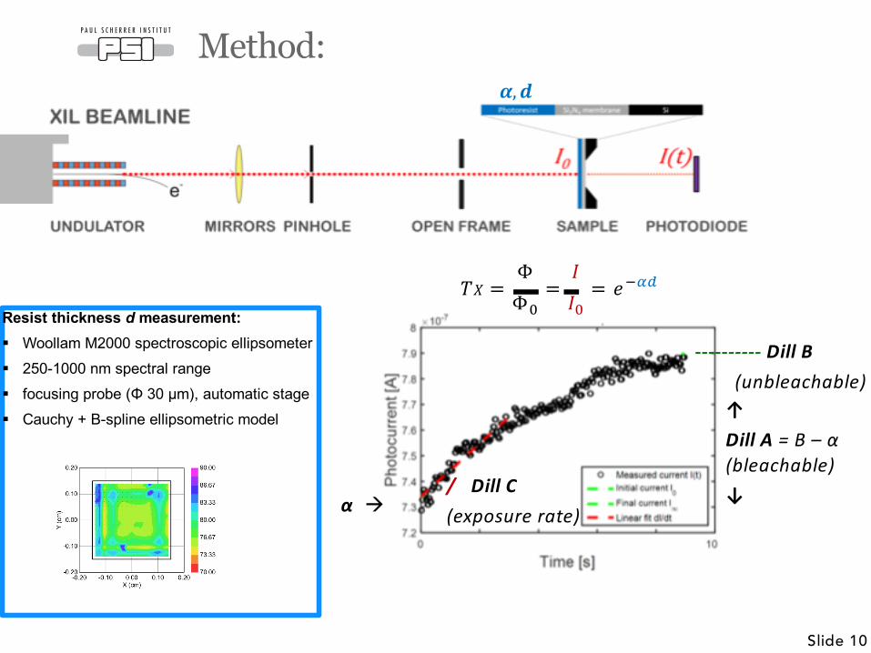
Method:
!" = ΦΦ%
= &&%= '()*
---------- Dill B(unbleachable)
α à/ Dill C(exposure rate)
↑Dill A = B – α(bleachable)↓
Slide 10
+,-
Resist thickness d measurement:§ Woollam M2000 spectroscopic ellipsometer§ 250-1000 nm spectral range§ focusing probe (Φ 30 μm), automatic stage§ Cauchy + B-spline ellipsometric model
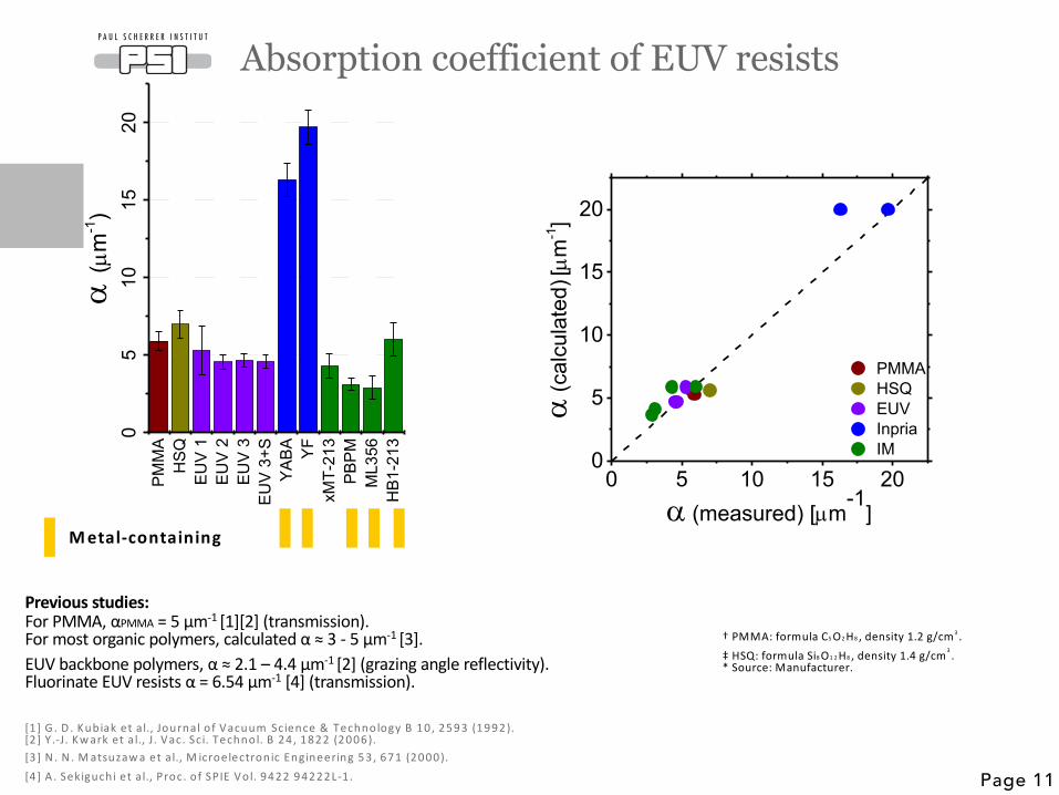
Absorption coefficient of EUV resists
Page 11
Previous studies:For PMMA, αPMMA = 5 μm-1 [1][2] (transmission).For most organic polymers, calculated α ≈ 3 - 5 μm-1 [3].EUV backbone polymers, α ≈ 2.1 – 4.4 μm-1 [2] (grazing angle reflectivity).Fluorinate EUV resists α = 6.54 μm-1 [4] (transmission).
[1] G . D . Kubiak et al., Journal of Vacuum Science & Technology B 10 , 2593 (1992). [2 ] Y .-J. Kw ark et al., J. Vac. Sci. Technol. B 24 , 1822 (2006).[3 ] N . N . M atsuzaw a et al., M icroelectronic Engineering 53 , 671 (2000).[4 ] A . Sekiguchi et al., Proc. of SPIE Vol. 9422 94222L-1 .
M etal-containing
† PMMA: formula C5 O2 H8 , density 1.2 g/cm3 .‡ HSQ: formula Si8 O1 2 H8 , density 1.4 g/cm3 .* Source: Manufacturer.
PMM
AH
SQEU
V 1
EUV
2EU
V 3
EUV
3+S
YABA YF
xMT-
213
PBPM
ML3
56H
B1-2
13
05
1015
20a
(µm
-1)
0 5 10 15 200
5
10
15
20
PMMAHSQEUVInpriaIM
a (c
alcu
late
d) [µ
m-1]
a (measured) [µm-1
]
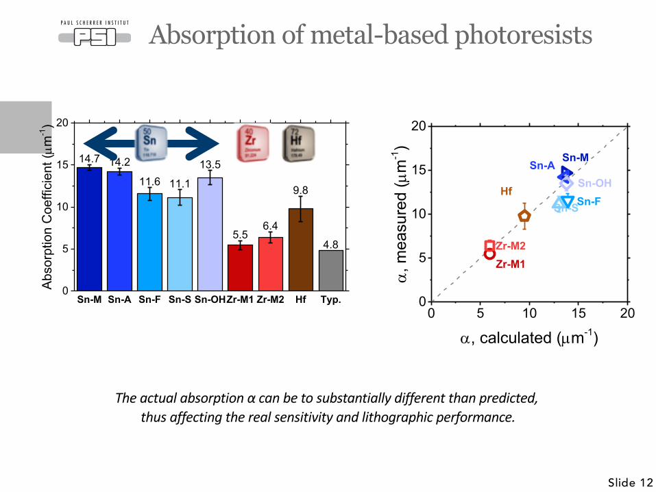
Sn-M Sn-A Sn-F Sn-S Sn-OHZr-M1 Zr-M2 Hf Typ.0
5
10
15
20
14.7 14.2
11.6 11.1
13.5
5.56.4
9.8
4.8
Abso
rptio
n C
oeffi
cien
t (µm
-1)
Absorption of metal-based photoresists
Slide 12
The actual absorption α can be to substantially different than predicted, thus affecting the real sensitivity and lithographic performance.
0 5 10 15 200
5
10
15
20
Sn-MSn-A
Sn-FSn-S
Sn-OH
Zr-M1Zr-M2
Hf
a, m
easu
red
(µm
-1)
a, calculated (µm-1)
PMMAHSQ
EUV 1EUV 2EUV 3
EUV 3+SYABA
YFxMT-213
PBPMML356
HB1-213
0 5 10 15 20B (µm-1)
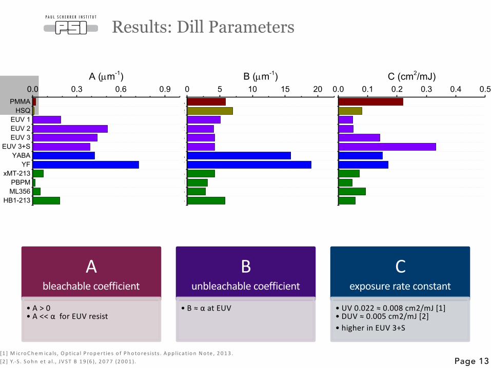
Results: Dill Parameters
Page 13
A bleachable coefficient
• A > 0• A << α for EUV resist
Bunbleachable coefficient
• B ≈ α at EUV
Cexposure rate constant
• UV 0.022 ≈ 0.008 cm2/mJ [1]• DUV ≈ 0.005 cm2/mJ [2]• higher in EUV 3+S
[1 ] M ic ro C h e m ica ls , O p t ica l P ro p e rt ie s o f P h o to re s ists . A p p lica t io n N o te , 2 0 1 3 .[2 ] Y.-S . S o h n e t a l. , JV S T B 1 9 (6 ), 2 0 7 7 (2 0 0 1 ).
PMMAHSQ
EUV 1EUV 2EUV 3
EUV 3+SYABA
YFxMT-213
PBPMML356
HB1-213
0.0 0.3 0.6 0.9A (µm-1)
0.0 0.1 0.2 0.3 0.4 0.5C (cm2/mJ)
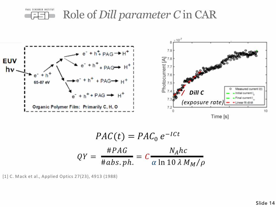
Role of Dill parameter C in CAR
[1] C. Mack et al., Applied Optics 27(23), 4913 (1988)
!"#(%) = !"#( )*+,-
Slide 14
/ Dill C(exposure rate)
./ = #!"1#234. 6ℎ. = # 89ℎ:
; ln 10 @ ⁄BC D
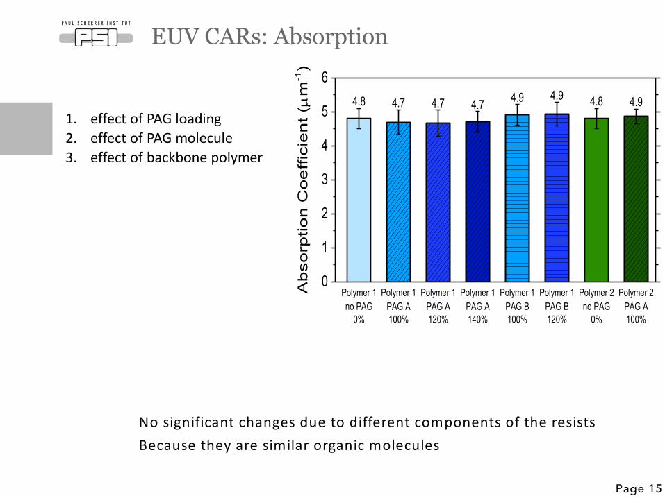
EUV CARs: Absorption
Page 15
Polymer 1 Polymer 1 Polymer 1 Polymer 1 Polymer 1 Polymer 1 Polymer 2 Polymer 20
1
2
3
4
5
64.8 4.7 4.7 4.7 4.9 4.9 4.8 4.9
Ab
sorp
tion
Co
effic
ien
t (µ
m-1)
no PAG PAG A PAG A PAG A PAG B PAG B no PAG PAG A0% 100% 120% 140% 100% 120% 0% 100%
1. effect of PAG loading2. effect of PAG molecule3. effect of backbone polymer
No significant changes due to different components of the resistsBecause they are similar organic molecules
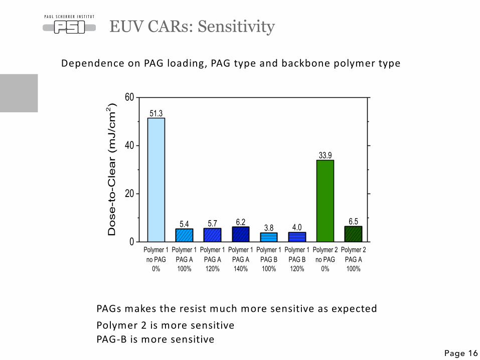
EUV CARs: Sensitivity
Page 16
Polymer 1 Polymer 1 Polymer 1 Polymer 1 Polymer 1 Polymer 1 Polymer 2 Polymer 20
20
40
6051.3
5.4 5.7 6.2 3.8 4.0
33.9
6.5
Do
se-t
o-C
lea
r (m
J/cm
2)
no PAG PAG A PAG A PAG A PAG B PAG B no PAG PAG A0% 100% 120% 140% 100% 120% 0% 100%
Dependence on PAG loading, PAG type and backbone polymer type
PAGs makes the resist much more sensitive as expectedPolymer 2 is more sensitivePAG-B is more sensitive
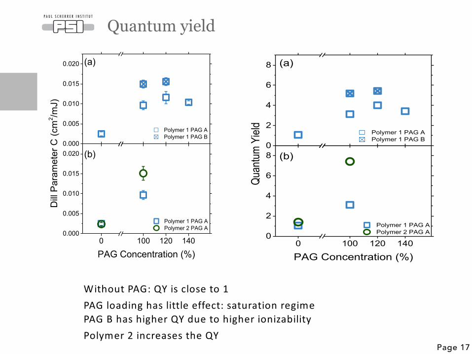
Quantum yield
Page 17
0.0 1.0 1.2 1.4
0.000
0.005
0.010
0.015
0.020
0 100 120 140
0.0 1.0 -- --
0.000
0.005
0.010
0.015
0.020
(a)
(b)
Dill
Para
met
er C
(cm
2 /mJ)
Polymer 1 PAG A Polymer 1 PAG B
PAG Concentration (%)
Polymer 1 PAG A Polymer 2 PAG A
0.0 1.0 1.2 1.4
0
2
4
6
8
0 100 120 140
0.0 1.0 -- --
0
2
4
6
8
(a)
(b)
Quan
tum
Yiel
d
Polymer 1 PAG A Polymer 1 PAG B
PAG Concentration (%)
Polymer 1 PAG A Polymer 2 PAG A
Without PAG: QY is close to 1PAG loading has little effect: saturation regimePAG B has higher QY due to higher ionizabilityPolymer 2 increases the QY
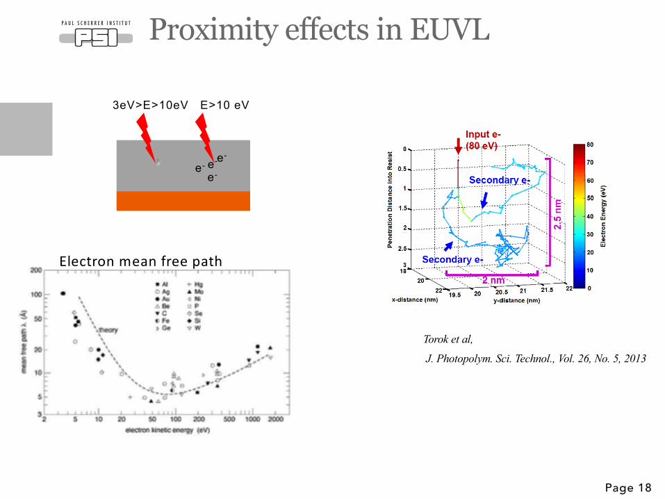
Proximity effects in EUVL
Page 18
Torok et al,
J. Photopolym. Sci. Technol., Vol. 26, No. 5, 2013
Electron mean free path
e-
e-e-e-
3eV>E>10eV E>10 eV
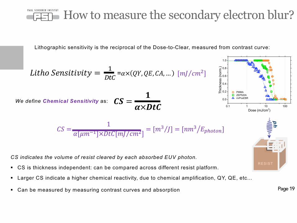
How to measure the secondary electron blur?
Page 19
We define Chemical Sensitivity as:
Lithographic sensitivity is the reciprocal of the Dose-to-Clear, measured from contrast curve:
!" =$
%×'(!
)*+ℎ- ./01*+*2*+3 =4
567=8× 9:,9<, =>,… [ ⁄BC DBE]
=. =1
8[HBI4]×J+=[ ⁄BC DBE]= [ ⁄BK C] = [ L0BK <MNO6OP]
CS indicates the volume of resist cleared by each absorbed EUV photon.
§ CS is thickness independent: can be compared across different resist platform.
§ Larger CS indicate a higher chemical reactivity, due to chemical amplification, QY, QE, etc...
§ Can be measured by measuring contrast curves and absorption
V
RESIST
ph
0.1 1 10 100
0.0
0.2
0.4
0.6
0.8
1.0
PMMA ZEP520A mrPosEBR
Thic
knes
s (n
orm
.)
Dose (mJ/cm2)
Plot Thickness Thickness ThicknessA1 0 ± 0 0 ± 0 0 ± 0A2 1 ± 0 1 ± 0 1.17186 ± 0.05857LOGx0 22.81965 ± 0.26052 14.62096 ± 0.21021 5.70293 ± 0.42013p -0.13825 ± 0.00973 -0.13712 ± 0.0076 -0.13949 ± 0.01315Reduced Chi-Sqr 0.00252 0.00262 0.00278R-Square(COD) 0.98697 0.97629 0.97761Adj. R-Square 0.98664 0.97567 0.97672
PMMAHSQ
EUV 1EUV 2EUV 3
EUV 3+SYABA
YFxMT-213
PBPMML356
HB1-213
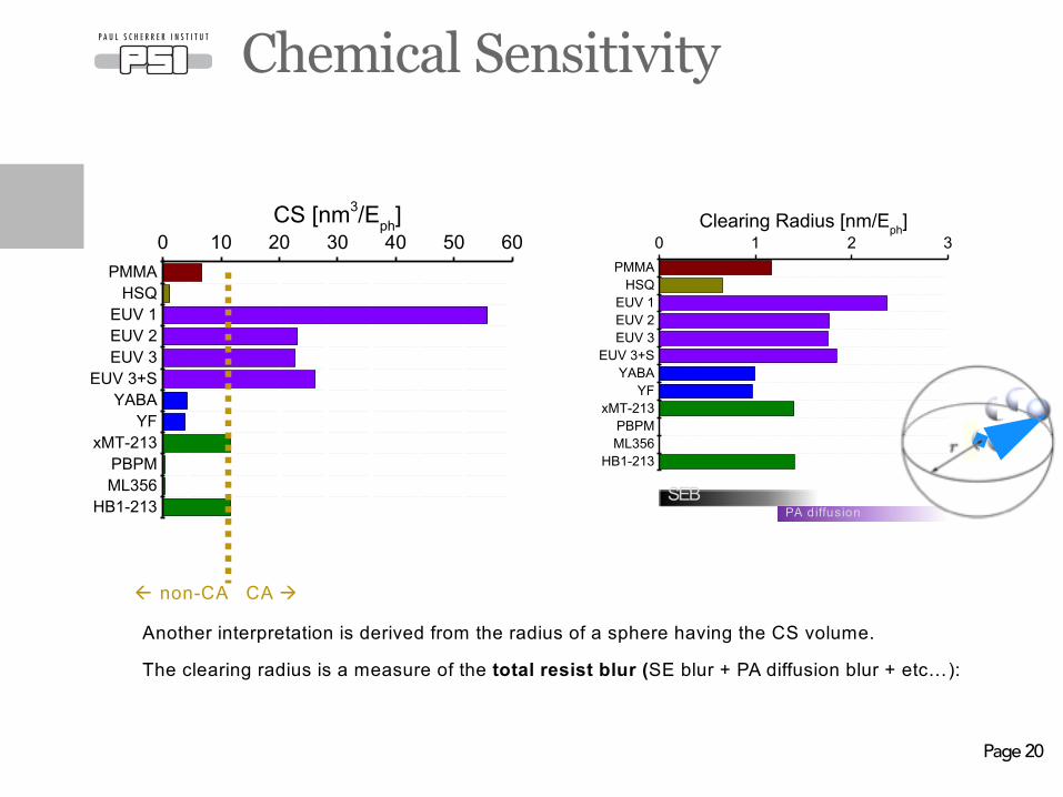
0 10 20 30 40 50 60CS [nm3/Eph]
Chemical Sensitivity
Page 20
ß non-CA CA à
PMMAHSQ
EUV 1EUV 2EUV 3
EUV 3+SYABA
YFxMT-213
PBPMML356
HB1-213
0 1 2 3Clearing Radius [nm/E
ph]
PA diffusionSEB
Another interpretation is derived from the radius of a sphere having the CS volume.
The clearing radius is a measure of the total resist blur (SE blur + PA diffusion blur + etc…):
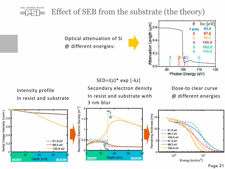
Effect of SEB from the substrate (the theory)
Page 21
Optical attenuation of Si@ different energies:
Intensity profileIn resist and substrate
Secondary electron densityIn resist and substrate with 3 nm blur
Dose-to clear curve@ different energies
SED=I(z)* exp [-λz]
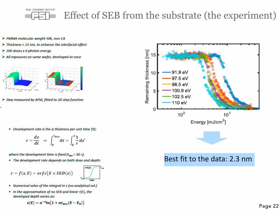
Effect of SEB from the substrate (the experiment)
Page 22
Best fit to the data: 2.3 nm
Summary
Page 23
• It is good news that EUV photons can make down to 7 nm hp.
• But we need to understand the fundamentals and reaction pathways
• Macroscopic parameters à Microscopic parameters
(dose, absorption, Dill’s parameters) (SEB, QE)
• For a state-of-the-art CAR: QY is 3-8• PAG-backbone interaction could be exploited to increase QY• SEB: For non-CAR=~1-2 nm and for CAR=4-5 nm
• To push the resolution limits of EUV lithography
• we need to understand the fundamentals
• We need to employ many analytical tools
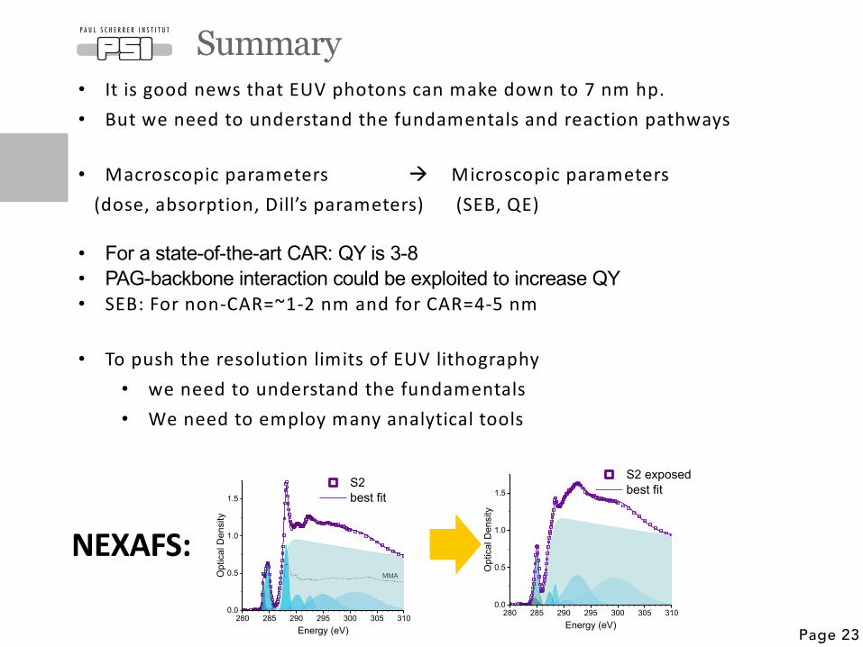
280 285 290 295 300 305 3100.0
0.5
1.0
1.5
Opt
ical
Den
sity
Energy (eV)
S2 best fit
MMA
280 285 290 295 300 305 3100.0
0.5
1.0
1.5O
ptic
al D
ensi
ty
Energy (eV)
S2 exposed best fit
NEXAFS:
Acknowledgments
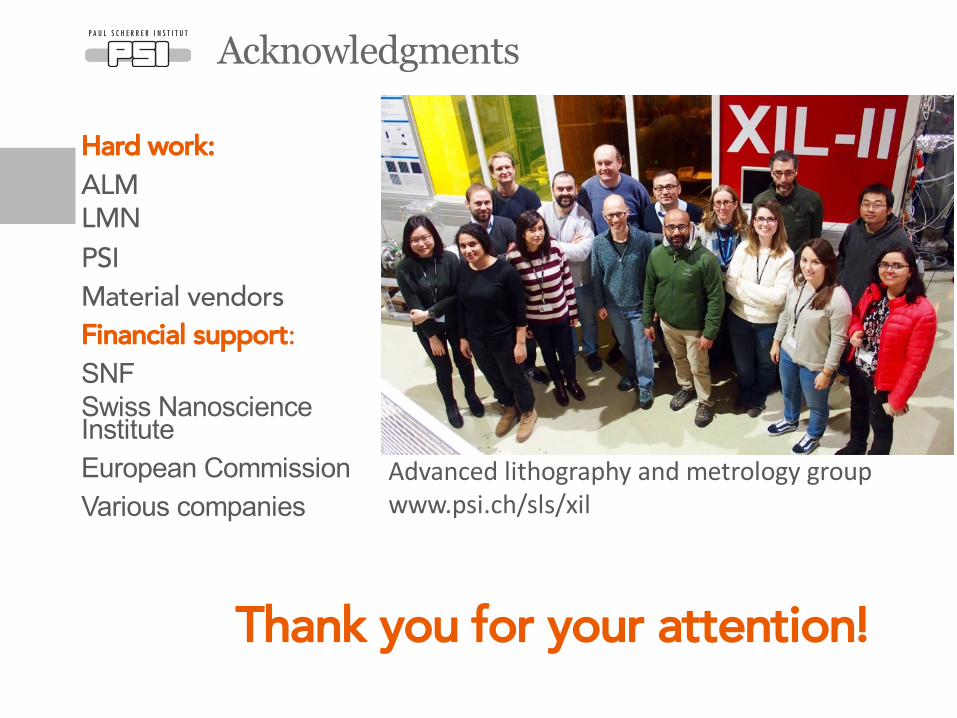
Hard work: ALMLMNPSIMaterial vendorsFinancial support:SNFSwiss Nanoscience InstituteEuropean CommissionVarious companies
Thank you for your attention!
Advanced lithography and metrology groupwww.psi.ch/sls/xil