Embed Size (px)
Citation preview

8227C–MCU Wireless–06/09
ZigBit™ 700/800/900 MHz Wireless Modules....................................................................................................................
ATZB-900-B0
Datasheet

ZigBit™ 700/800/900 MHz Wireless Modules 1-2
8227C–MCU Wireless–06/09

ZigBit™ 700/800/900 MHz Wireless Modules 1-i
8227C–MCU Wireless–06/09
Section 11.1 Summary............................................................................................................................ 1-1
1.2 Applications........................................................................................................................ 1-1
1.3 Key Features...................................................................................................................... 1-2
1.4 Benefits .............................................................................................................................. 1-2
1.5 Abbreviations and Acronyms ............................................................................................. 1-2
1.6 Related Documents............................................................................................................ 1-3
Section 22.1 Overview ............................................................................................................................ 2-1
Section 33.1 Electrical Characteristics.................................................................................................... 3-3
3.1.1 Absolute Maximum Ratings ................................................................................. 3-3
3.1.2 Test Conditions.................................................................................................... 3-3
3.1.3 RF Characteristics ............................................................................................... 3-4
3.1.4 ATmega1281V Microcontroller Characteristics ................................................... 3-4
3.1.5 Module Interfaces characteristics ........................................................................ 3-5
3.2 Physical/Environmental Characteristics and Outline.......................................................... 3-5
3.3 Pin Configuration................................................................................................................ 3-6
3.4 Mounting Information ......................................................................................................... 3-9
3.5 Soldering Profile............................................................................................................... 3-10
3.6 Antenna Reference Design .............................................................................................. 3-10
3.6.1 General recommendations ................................................................................ 3-11
Section 44.1 Ordering Information ........................................................................................................ 4-12

ZigBit™ 700/800/900 MHz Wireless Modules 1-1
8227C–MCU Wireless–06/09
Section 1
Introduction
1.1 Summary
ZigBit™ 900 is an ultra-compact, extended range, low-power, high-sensitivity 784/868/915 MHzIEEE 802.15.4/ZigBee® OEM module, based on the innovative Atmel’s mixed-signal hardware platform.It is designed for wireless sensing, control and data acquisition applications. ZigBit modules eliminatethe need for costly and time-consuming RF development, and shortens time to market for a wide rangeof wireless applications.
This module is the latest addition to the ZigBit family also represented by 2.4 GHz modules ATZB-24-A2/B0 [1], and ATZB-A24-UFL/U0 [3].
1.2 Applications
ZigBit 900 module is compatible with robust IEEE 802.15.4/ZigBee stack that supports a self-healing,self-organizing mesh network, while optimizing network traffic and minimizing power consumption. Atmeloffers two stack configurations: BitCloud and SerialNet. BitCloud is a ZigBee PRO certified softwaredevelopment platform supporting reliable, scalable, and secure wireless applications running on Atmel’sZigBit modules. SerialNet allows programming of the module via serial AT-command interface.
The applications include, but are not limited to:
• Building automation & monitoring– Lighting controls– Wireless smoke and CO detectors– Structural integrity monitoring
• HVAC monitoring & control• Inventory management• Environmental monitoring• Security• Water metering• Industrial monitoring
– Machinery condition and performance monitoring– Monitoring of plant system parameters such as temperature, pressure, flow, tank level, humidity,
vibration, etc.• Automated meter reading (AMR)

Introduction
ZigBit™ 700/800/900 MHz Wireless Modules 1-2
8227C–MCU Wireless–06/09
1.3 Key Features• Ultra compact size (18.8 x 13.5 mm)• High RX sensitivity (-110 dBm)• Outperforming link budget (120 dB)• Up to 11 dBm output power• Very low power consumption (< 6 µA in Sleep mode)• Ample memory resources (128K bytes of flash memory, 8K bytes RAM, 4K bytes EEPROM)• Wide range of interfaces (both analog and digital):
– 9 spare GPIO, 2 spare IRQ lines– 4 ADC lines + 1 line for supply voltage control (up to 9 lines with JTAG disabled)– UART with CTS/RTS control– USART– I2C– SPI– 1-Wire– Up to 30 lines configurable as GPIO
• Capability to write own MAC address into the EEPROM• Optional antenna reference designs• IEEE 802.15.4 compliant transceiver• 868 / 915 MHz band• 784 MHz Chinese band• BitCloud embedded software, including serial bootloader and AT command set
1.4 Benefits• Over 6 km (4 miles) outdoor line-of-sight range• Small physical footprint and low profile for optimum fit in even the smallest of devices(1)
• Extended battery life• Mesh networking capability• Easy-to-use low cost Evaluation Kit• Single source of support for HW and SW
Note: 1. The module is to be certified
1.5 Abbreviations and Acronyms
ADC Analog-to -Digital Converter
API Application Programming Interface
BPSK Binary Phase-Shift Keying modulation scheme
DC Direct Current
DTR Data Terminal Ready
EEPROM Electrically Erasable Programmable Read-Only Memory
ESD Electrostatic Discharge

Introduction
ZigBit™ 700/800/900 MHz Wireless Modules 1-3
8227C–MCU Wireless–06/09
1.6 Related Documents
[1] ZigBit™ 2.4 GHz Wireless Modules ATZB-24-A2/B0 Datasheet. Atmel’s doc8226.pdf
[2] ZigBit™ Development Kit. User Guide. MeshNetics Doc. S-ZDK-451 - TBD
[3] ZigBit™ Amplified 2.4 GHz Wireless Modules datasheet. Atmel’s doc8228.pdf
GPIO General Purpose Input/Output
HVAC Heating, Ventilating and Air Conditioning
HW Hardware
I2C Inter-Integrated Circuit
IEEE Institute of Electrical and Electrionics Engineers
IRQ Interrupt Request
ISM Industrial, Scientific and Medical radio band
JTAGDigital interface for debugging of embedded device, also known as IEEE 1149.1 standard interface
MAC Medium Access Control layer
MCUMicrocontroller Unit. In this document it also means the processor, which is the core of ZigBit module
O-QPSK Offset Quadrature Phase-Shift Keying modulation scheme
OEM Original Equipment Manufacturer
OTA Over-The-Air upgrade
PCB Printed Circuit Board
PER Package Error Ratio
RAM Random Access Memory
RF Radio Frequency
RTS/CTS Request to Send/ Clear to Send
RX Receiver
SMA Surface Mount Assembly
SPI Serial Peripheral Interface
SW Software
TTM Time To Market
TX Transmitter
UART Universal Asynchronous Receiver/Transmitter
USART Universal Synchronous/Asynchronous Receiver/Transmitter
USB Universal Serial Bus
ZDK ZigBit Development Kit
ZigBee, ZigBee PRO
Wireless networking standards targeted at low-power applications
802.15.4 The IEEE 802.15.4-2006 standard applicable to low-rate wireless Personal Area Network

Introduction
ZigBit™ 700/800/900 MHz Wireless Modules 1-4
8227C–MCU Wireless–06/09
[4] Atmel 8-bit AVR Microcontroller with 64K/128K/256K Bytes In-System Programmable Flash. 2549FAVR 04/06
[5] Atmel AT86RF212 Low Power 800/900 MHz Transceiver for IEEE 802.15.4b, Zigbee, and ISM Appli-cations. Preliminary specification
[6] Ultra Small Surface Mount Coaxial Connectors - Low Profile 1.9mm or 2.4mm Mated Height.http://www.hirose.co.jp/cataloge_hp/e32119372.pdf
[7] ZigBit 900 Development Kit. User's Guide. MeshNetics Doc. S-ZDK-451~03 TBD
[8] IEEE Std 802.15.4-2006 IEEE Standard for Information technology - Part 15.4 Wireless MediumAccess Control (MAC) and Physical Layer (PHY) Specifications for Low-Rate Wireless Personal AreaNetworks (LR-WPANs)
[9] ZigBee Specification. ZigBee Document 053474r17, October 19, 2007
[10] BitCloud™ IEEE 802.15.4/ZigBee Software. AVR2050: BitCloud User Guide. Atmel’s doc8199.pdf

ZigBit™ 700/800/900 MHz Wireless Modules 2-1
8227C–MCU Wireless–06/09
Section 2
Zigbit™700/800/900 MHz Wireless Modules Overview
2.1 Overview
ZigBit 900 is an extended-range low-power, a low-power, high-sensitivity IEEE 802.15.4/ ZigBee-compli-ant OEM module, which occupies less than a square inch. Based on a solid combination of Atmel’s latestMCU Wireless hardware platform [5], power amplifier and low-noise amplifier, the ZigBit 900 offers supe-rior radio performance, ultra-low power consumption and exceptional ease of integration.
Figure 2-1. ATZB-900-B0 Block Diagram
ZigBit 900 contains Atmel’s ATmega1281V Microcontroller [4] and AT86RF212 RF Transceiver [5]. Themodule features 128 Kbytes flash memory and 8 Kbytes RAM.
The ZigBit 900 already contains a complete RF/MCU-related design with all the necessary passive com-ponents included. The module can be easily mounted on a simple 2-layer PCB with a minimum ofrequired external connection. Compared to a custom RF/MCU design, a module-based solution offersconsiderable savings in development time and NRE cost per unit during the design, prototyping, andmass production phases of product development.
To jumpstart evaluation and development, Atmel also offers a complete set of evaluation and develop-ment tools. The new ZigBit 900 Development Kit [7] comes with everything you need to create customapplications featuring ZigBit 900 module.
The kit features MeshBean development boards (ATZB-EVB-900-SMA) with an easy-to-access exten-sion connector for attaching third party sensors and other peripherals, and a JTAG connector for easyapplication uploading and debugging.
The kit also includes reference applications to speed up application development, source code for hard-ware interface layer and reference drivers for the all the module interfaces, intuitive developmentenvironment from Atmel, and comprehensive set of application notes and product documentation.
ATmega1281AT86RF212
RFTranceiver
VCC (1.8 - 3.6V)
RF I/O
GPIO SPI Bus
IRQUART
USART/SPII2C
JTAGANALOG

Zigbit™700/800/900 MHz Wireless Modules Overview
ZigBit™ 700/800/900 MHz Wireless Modules 2-2
8227C–MCU Wireless–06/09
ZigBit 900 modules come bundled with BitCloud, a 2nd generation embedded software stack from Atmel.BitCloud is fully compliant with ZigBee PRO and ZigBee standards for wireless sensing and control [8],[9], [10] and it provides an augmented set of APIs which, while maintaining 100% compliance with thestandard, offer extended functionality designed with developer's convenience and ease-of-use in mind.
Depending on end-user design requirements, ZigBit 900 can operate as a self-contained sensor node,where it would function as a single MCU, or it can be paired with a host processor driving the moduleover a serial interface. In the former case, a user application may be used with the BitCloud softwareallowing customization of embedded applications through BitCloud’s C API.
In the latter case, the host processor controls data transmission and manages module peripherals via anextensive set of SerialNet AT commands. Thus, no firmware customization is required for a successfulmodule design-in. Additionally, third-party sensors can be connected directly to the module, thusexpanding the existing set of peripheral interfaces.

ZigBit™ 700/800/900 MHz Wireless Modules 3-3
8227C–MCU Wireless–06/09
Section 3
Specifications
3.1 Electrical Characteristics
3.1.1 Absolute Maximum Ratings
Notes: 1. Absolute Maximum Ratings are the values beyond which damage to the device may occur. Under nocircumstances must the absolute maximum ratings given in this table be violated. Stresses beyondthose listed under "Absolute Maximum Ratings" may cause permanent damage to the device.
This is a stress rating only. Functional operation of the device at these or other conditions, beyond thoseindicated in the operational sections of this specification, is not implied. Exposure to absolute maximumrating conditions for extended periods may affect device reliability.
2. Attention! ZigBit 900 is an ESD-sensitive device. Precaution should be taken when handling the devicein order to prevent permanent damage.
3.1.2 Test Conditions
Note: 1. Preliminary data
Current consumption actually depends on multiple factors, including but not limited to, the board designand materials, BitCloud settings, network activity, EEPROM read/write operations. It also depends onMCU load and/or peripherals used by an application.
Table 3-1. Absolute Maximum Ratings(1)(2)
Parameters Min Max
Voltage on any pin, except RESET with respect to Ground -0.5V VCC + 0.5V
DC Current per I/O Pin 40 mA
DC Current DVCC and DGND pins 300 mA
Input RF Level +5 dBm
Table 3-2. Test conditions (unless otherwise stated), VCC = 3V, Tamb = 25°C
Parameters Condition Range Unit
Supply Voltage, VCC 1.8 to 3.6 V
Current Consumption: RX mode(1) 15 mA
Current Consumption: TX mode(1) PTX = 5 dBm 20 mA
Current Consumption: Power-save mode(1) 6 µA

Specifications
ZigBit™ 700/800/900 MHz Wireless Modules 3-4
8227C–MCU Wireless–06/09
3.1.3 RF Characteristics
Notes: 1. Preliminary data2. IEEE 802.15.4-2006 compliant
3.1.4 ATmega1281V Microcontroller Characteristics
Table 3-3. RF Characteristics
Parameters Condition Range Unit
Frequency Band
779 to 787
868 to 868.6
902 to 928
MHz
Number of Channels 15
Channel Spacing 2 MHz
Transmitter Output Power -11 to +11 dBm
Receiver Sensitivity AWGN channel, PER = 1%
20 kbit/s(2)
PSDU length of 20 octets
-110
dBm
40 kbit/s(2) -108
100 kbit/s(2) -101
250 kbit/s(2) -100
200 kbit/s
PSDU length of 127 octets
-97
400 kbit/s -90
500 kbit/s -97
1000 kbit/s -92
On-Air Data Rate
BPSK modulation20 (at 868 MHz),
40 (at 915 MHz)
kbps
O-QPSK modulation100 (at 868 MHz)
250 (at 915 MHz and 784 MHz)
TX Output/ RX Input Nominal Impedance For balanced output 100 Ω
Range, outdoors(1) For balanced output 6 km
Table 3-4. ATmega1281V Characteristics
Parameters Condition Range Unit
On-chip Flash Memory size 128 Kbytes
On-chip RAM size 8 Kbytes
On-chip EEPROM size 4 Kbytes
Operation Frequency 4 MHz
Specifications
ZigBit™ 700/800/900 MHz Wireless Modules 3-5
8227C–MCU Wireless–06/09
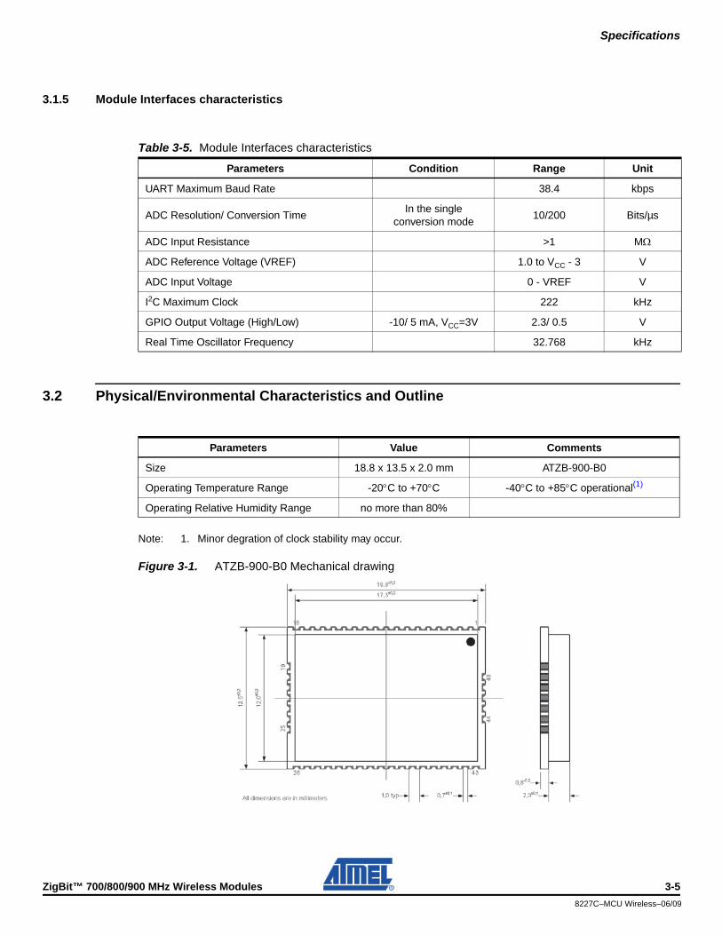
3.1.5 Module Interfaces characteristics
3.2 Physical/Environmental Characteristics and Outline
Note: 1. Minor degration of clock stability may occur.
Figure 3-1. ATZB-900-B0 Mechanical drawing
Table 3-5. Module Interfaces characteristics
Parameters Condition Range Unit
UART Maximum Baud Rate 38.4 kbps
ADC Resolution/ Conversion TimeIn the single
conversion mode10/200 Bits/µs
ADC Input Resistance >1 MΩ
ADC Reference Voltage (VREF) 1.0 to VCC - 3 V
ADC Input Voltage 0 - VREF V
I2C Maximum Clock 222 kHz
GPIO Output Voltage (High/Low) -10/ 5 mA, VCC=3V 2.3/ 0.5 V
Real Time Oscillator Frequency 32.768 kHz
Parameters Value Comments
Size 18.8 x 13.5 x 2.0 mm ATZB-900-B0
Operating Temperature Range -20°C to +70°C -40°C to +85°C operational(1)
Operating Relative Humidity Range no more than 80%

Specifications
ZigBit™ 700/800/900 MHz Wireless Modules 3-6
8227C–MCU Wireless–06/09
3.3 Pin Configuration
Figure 3-2. ATZB-900-B0 Pinout
Table 3-6. Pin descriptions
Connector Pin Pin Name Description I/O
Default State after Power on
1 SPI_CLK Reserved for stack operation(4) O
2 SPI_MISO Reserved for stack operation(4) I/O
3 SPI_MOSI Reserved for stack operation(4) I/O
4 GPIO0 General Purpose digital Input/Output 0(2)(3)(4)(7) I/O tri-state
5 GPIO1 General Purpose digital Input/Output 1(2)(3)(4)(7) I/O tri-state
6 GPIO2 General Purpose digital Input/Output 2(2)(3)(4)(7) I/O tri-state
7 OSC32K_OUT 32.768 kHz clock output(4)(5) O
8 RESET Reset input (active low)(4)
9,22,23 DGND Digital Ground
10 CPU_CLK
RF clock output. When module is in active state, 4 MHz signal is present on this line. While module
is in the sleeping state, clock generation is also stopped(4).
O
11 I2C_CLK I2C serial clock output(2)(3)(4)(7) O tri-state
12 I2C_DATA I2C serial clock input/output(2)(3)(4)(7) I/O tri-state
13 UART_TXD UART transmit output(1)(2)(3)(4)(7) O tri-state
14 UART_RXD UART receive input(1)(2)(3)(4)(7) I tri-state
15 UART_RTSRTS input (Request To send) for UART hardware
flow control. Active low(2)(3)(4)(7) I tri-state

Specifications
ZigBit™ 700/800/900 MHz Wireless Modules 3-7
8227C–MCU Wireless–06/09
Notes: 1. The UART_TXD pin is intended for input (i.e. its designation as "TXD" implies some complex systemcontaining ZigBit 900 as its RF terminal unit), while UART_RXD pin, vice versa, is for output.
2. Most of pins can be configured for general purpose I/O or for some alternate functions as described indetails in the ATmega1281V Datasheet [1].
3. GPIO pins can be programmed either for output, or for input with/without pull-up resistors. Output pindrivers are strong enough to drive LED displays directly (refer to figures on pages 387-388, [1]).
4. All digital pins are provided with protection diodes to D_VCC and DGND
16 UART_CTSCTS output (Clear To send) for UART hardware
flow control. Active low(2)(3)(4)(7) O tri-state
17 GPIO6 General Purpose digital Input/Output 6(2)(3)(4)(7) I/O tri-state
18 GPIO7 General Purpose digital Input/Output 7(2)(3)(4)(7) I/O tri-state
19 GPIO3 General Purpose digital Input/Output 3(2)(3)(4)(7) I/O tri-state
20 GPIO4 General Purpose digital Input/Output 4(2)(3)(4)(7) I/O tri-state
21 GPIO5 General Purpose digital Input/Output 5(2)(3)(4)(7) I/O tri-state
24,25 D_VCC Digital Supply Voltage (VCC)(9)
26 JTAG_TMS JTAG Test Mode Select(2)(3)(4)(6) I
27 JTAG_TDI JTAG Test Data Input(2)(3)(4)(6) I
28 JTAG_TDO JTAG Test Data Output(2)(3)(4)(6) O
29 JTAG_TCK JTAG Test Clock(2)(3)(4)(6) I
30 ADC_INPUT_3 ADC Input Channel 3(2)(3)(7) I tri-state
31 ADC_INPUT_2 ADC Input Channel 2(2)(3)(7) I tri-state
32 ADC_INPUT_1 ADC Input Channel 1(2)(3)(7) I tri-state
33 BATADC Input Channel 0, used for battery level measurement. This pin equals VCC/3.(2)(3)(7) I tri-state
34 A_VREF Input/Output reference voltage for ADC I/O tri-state
35 AGND Analog ground
36 GPIO_1WR 1-wire interface(2)(3)(4)(7) I/O
37 UART_DTRDTR input (Data Terminal Ready) for UART.
Active low(2)(3)(4)(7) I tri-state
38 USART0_RXD USART/SPI Receive pin(2)(3)(4)(7) I tri-state
39 USART0_TXD USART /SPI Transmit pin(2)(3)(4)(7) O tri-state
40 USART0_EXTCLK USART/SPI External Clock(2)(3)(4)(7) I/O tri-state
41 GPIO8 General Purpose Digital Input/Output 8(2)(3)(4)(7) I/O tri-state
42 IRQ_7 Digital Input Interrupt request 7(2)(3)(4)(7) I tri-state
43 IRQ_6 Digital Input Interrupt request 6(2)(3)(4)(7) I tri-state
44,46,48 RF GND RF Analog Ground
45 RFP_IO Differential RF Input/Output I/O
47 RFN_IO Differential RF Input/Output I/O
Table 3-6. Pin descriptions (Continued)
Connector Pin Pin Name Description I/O
Default State after Power on

Specifications
ZigBit™ 700/800/900 MHz Wireless Modules 3-8
8227C–MCU Wireless–06/09
5. It is strongly recommended to avoid assigning an alternate function for OSC32K_OUT pin because it isused by BitCloud. However, this signal can be used if another peripheral or host processor requires32.768 kHz clock, otherwise this pin can be disconnected.
6. Normally, JTAG_TMS, JTAG_TDI, JTAG_TDO, JTAG_TCK pins are used for on-chip debugging andflash burning. They can be used for A/D conversion if JTAGEN fuse is disabled.
7. The following pins can be configured with the BitCloud software to be general-purpose I/O lines:GPIO0, GPIO1, GPIO2, GPIO3, GPIO4, GPIO5, GPIO6, GPIO7, GPIO8, GPIO_1WR, I2C_CLK,I2C_DATA, UART_TXD, UART_RXD, UART_RTS, UART_CTS, ADC_INPUT_3, ADC_INPUT_2,ADC_INPUT_1, BAT, UART_DTR, USART0_RXD, USART0_TXD, USART0_EXTCLK, IRQ_7, IRQ_6.Additionally, four JTAG lines can be programmed with software as GPIO as well, but this requireschanging the fuse bits and will disable JTAG debugging.
8. With BitCloud, CTS pin can be configured to indicate sleep/active condition of the module thus provid-ing mechanism for power management of host processor. If this function is necessary, connection ofthis pin to external pull-down resistor is recommended to prevent the undesirable transients duringmodule reset process.
9. Using ferrite bead and 1 µF capacitor located closely to the power supply pin is recommended, asshown below.
10. In SPI mode, USART0_EXTCLK is output. In USART mode, this pin can be configured as either input oroutput pin.

Specifications
ZigBit™ 700/800/900 MHz Wireless Modules 3-9
8227C–MCU Wireless–06/09
Figure 3-3. Typical Reference Schematic
3.4 Mounting Information
The below diagrams show the PCB layout recommended for ZigBit 900 module. Neither via-holes norwires are allowed on the PCB upper layer in area occupied by the module. As a critical requirement,RF_GND pins should be grounded via several holes to be located right next to the pins thus minimizinginductance and preventing both mismatch and losses.
SPI_CLK
SPI_MISO
SPI_MOSI
GPIO0
GPIO1
GPIO2
OSC32K_OUT
RESET
DGND
CPU_CLK
I2C_CLK
I2C_DATA
UART_TXD
UART_RXD
UART_RTS
UART_CTS
GPIO6
GPIO7
GPIO3
GPIO4
GPIO5
DGND
DGND
D_VCC
D_VCC
123456789101112131415161718
19202122232425
JTAG_TMS
JTAG_TDI
JTAG_TDO
JTAG_TCK
ADC_INPUT_3
ADC_INPUT_2
ADC_INPUT_1
BAT
A_VREF
AGND
GPIO9
UART_DTR
USART0_RXD
USART0_TXD
USART0_EXTCLK
GPIO8
IRQ_7
IRQ_6
RF_GND
RFP_IO
RF_GND
RFN_IO
RF_GND
262728293031323334353637383940414243
JTAG_VCC
NC
JTAG_TCK
JTAG_TDI
JTAG_TDO
JTAG_TMS
NC
JTAG_RST
59314786
JTAG_GND2
JTAG_GND10
100k
1uF
Host MCU
UART_CTS
UART_RTS
UART_TXD
UART_RXD
VCC1,8..3,6V *) 68 pF
GRM 1555C1H101JZ01D
VCC
RST
4445464748
Balun0900BL18B100
56
4
3
12two capacitors*

Specifications
ZigBit™ 700/800/900 MHz Wireless Modules 3-10
8227C–MCU Wireless–06/09
Figure 3-4. ATZB-900-B0 PCB Recommended Layout, Top View
3.5 Soldering Profile
The J-STD-020C-compliant soldering profile is recommended, as given below.
Note: 1. The package is backward compatible with Pb/Sn soldering profile
3.6 Antenna Reference Design
This section presents PCB design which may be used to combine ZigBit 900 with an external antennaThis antenna reference designs is recommended for successful design-in.
Table 3-7. Soldering Profile(1)
Profile Feature Green Package
Average ramp-up rate (217 °C to peak) 3 °C/s max.
Preheat temperature 175 °C ± 25 °C 180 s max.
Temperature maintained above 217 °C 60 s to 150 s
Time within 5 °C of actual peak temperature 20 s to 40 s
Peak temperature range 6 °C/s max.
Ramp-down rate 8 minutes max.

Specifications
ZigBit™ 700/800/900 MHz Wireless Modules 3-11
8227C–MCU Wireless–06/09
Figure 3-5. FCC/CE compliant RF reference design with RP-SMA connector recommended for ATZB-900-B0
Multiple factors affect proper antenna match, hence, affecting the antenna pattern. The particular factorsare the board material and thickness, shields, the material used for enclosure, the board neighborhood,and other components adjacent to antenna.
3.6.1 General recommendations
Metal enclosure should not be used. Using low profile enclosure might also affect antenna tuning.
Placing high profile components next to antenna should be avoided.
Having holes punched around the periphery of the board eliminates parasitic radiation from the board edges also distorting antenna pattern.
ZigBit 900 module should not be placed next to the consumer electronics which might interfere with ZigBit 900's RF frequency band.
The board design should prevent propagation of microwave field inside the board material. Electromag-netic waves of high frequency may penetrate the board thus making the edges of the board radiate,which may distort the antenna pattern. To eliminate this effect, metalized and grounded holes must beplaced around the board's edges.

ZigBit™ 700/800/900 MHz Wireless Modules 4-12
8227C–MCU Wireless–06/09
Section 4
Ordering Information
4.1 Ordering Information
Note: 1. Tape and Reel quantity: 200
Part Number Description
ATZB-900-B0R(1) 783/868/915 MHz IEEE802.15.4/ZigBee Wireless Module w/ Balanced RF Port

8227C–MCU Wireless–06/09
© 2009 Atmel Corporation. All rights reserved. Atmel®, Atmel logo and combinations thereof, and others are registered trademarks or trade-marks of Atmel Corporation or its subsidiaries. Other terms and product names may be trademarks of others.
Headquarters International
Atmel Corporation2325 Orchard ParkwaySan Jose, CA 95131USATel: 1(408) 441-0311Fax: 1(408) 487-2600
Atmel AsiaUnit 1-5 & 16, 19/FBEA Tower, Millennium City 5418 Kwun Tong RoadKwun Tong, KowloonHong KongTel: (852) 2245-6100Fax: (852) 2722-1369
Atmel EuropeLe Krebs8, Rue Jean-Pierre TimbaudBP 30978054 Saint-Quentin-en-Yvelines CedexFranceTel: (33) 1-30-60-70-00 Fax: (33) 1-30-60-71-11
Atmel Japan9F, Tonetsu Shinkawa Bldg.1-24-8 ShinkawaChuo-ku, Tokyo 104-0033JapanTel: (81) 3-3523-3551Fax: (81) 3-3523-7581
Product Contact
Web Sitewww.atmel.com
Technical [email protected]
Sales Contactwww.atmel.com/contacts
Literature Requestswww.atmel.com/literature
Disclaimer: The information in this document is provided in connection with Atmel products. No license, express or implied, by estoppel or otherwise, to anyintellectual property right is granted by this document or in connection with the sale of Atmel products. EXCEPT AS SET FORTH IN ATMEL’S TERMS AND CONDI-TIONS OF SALE LOCATED ON ATMEL’S WEB SITE, ATMEL ASSUMES NO LIABILITY WHATSOEVER AND DISCLAIMS ANY EXPRESS, IMPLIED OR STATUTORYWARRANTY RELATING TO ITS PRODUCTS INCLUDING, BUT NOT LIMITED TO, THE IMPLIED WARRANTY OF MERCHANTABILITY, FITNESS FOR A PARTICULARPURPOSE, OR NON-INFRINGEMENT. IN NO EVENT SHALL ATMEL BE LIABLE FOR ANY DIRECT, INDIRECT, CONSEQUENTIAL, PUNITIVE, SPECIAL OR INCIDEN-TAL DAMAGES (INCLUDING, WITHOUT LIMITATION, DAMAGES FOR LOSS OF PROFITS, BUSINESS INTERRUPTION, OR LOSS OF INFORMATION) ARISING OUT OFTHE USE OR INABILITY TO USE THIS DOCUMENT, EVEN IF ATMEL HAS BEEN ADVISED OF THE POSSIBILITY OF SUCH DAMAGES. Atmel makes norepresentations or warranties with respect to the accuracy or completeness of the contents of this document and reserves the right to make changes to specificationsand product descriptions at any time without notice. Atmel does not make any commitment to update the information contained herein. Unless specifically providedotherwise, Atmel products are not suitable for, and shall not be used in, automotive applications. Atmel’s products are not intended, authorized, or warranted for useas components in applications intended to support or sustain life.
![Módulo OEM ZigBit 900 - Nextfor - ZigBit 900.pdf · plataforma hardware AVR Z-Link de Atmel [1], el ZigBit 900 ofrece una prestación de radio superior con una excepcional facilidad](https://img.pdfslide.net/doc/110x75/5e9297195970022bd57a76cc/mdulo-oem-zigbit-900-zigbit-900pdf-plataforma-hardware-avr-z-link-de-atmel.jpg)


![ZigBit 2.4GHz Wireless Modules ATZB-24-A2/B0...ATZB-24-A2/B0 [ZigBit 2.4GHz Wireless Modules] 8226C−AVR−07/2013 3 1. Introduction 1.1 Summary ZigBit® is an ultra-compact, low-power,](https://img.pdfslide.net/doc/110x75/6103dcd6e905b36a8459cc67/zigbit-24ghz-wireless-modules-atzb-24-a2b0-atzb-24-a2b0-zigbit-24ghz-wireless.jpg)