Embed Size (px)
Citation preview

ZSPM1025A / ZSPM1035A Programming and Calibration
© 2016 Integrated Device Technology, Inc. 1 April 7, 2016
Contents 1 Introduction ....................................................................................................................................................... 2 2 Basic Access to OTP Data ............................................................................................................................... 2
2.1.1. Read Procedure .................................................................................................................................. 2 2.1.2. Write Procedure .................................................................................................................................. 2 2.1.3. Simple Tests ....................................................................................................................................... 3
3 Configuration Programming ............................................................................................................................. 3 3.1. Format of the ROM File ............................................................................................................................. 3
4 External Temperature Calibration .................................................................................................................... 4 4.1. Requirements ............................................................................................................................................ 4 4.2. Calibration Procedure ................................................................................................................................ 4 4.3. Correction Procedure for Ambient Temperatures Other than 25°C .......................................................... 5 4.4. Calculation Examples for Ambient Temperatures Other than 25°C .......................................................... 5 4.5. Additional Information for Temperature Calibration .................................................................................. 5
5 Current Calibration Procedure.......................................................................................................................... 6 5.1. Requirements ............................................................................................................................................ 6 5.2. Calibration Procedure ................................................................................................................................ 6 5.3. Computation of Current Sense Correction Factors ................................................................................... 7 5.4. DCR Temperature Correction during Calibration ...................................................................................... 7 5.5. Calculation Examples ................................................................................................................................ 8
6 PMBus™ Command Reference ..................................................................................................................... 10 6.1. Overview about PMBus™ Commands .................................................................................................... 10 6.2. PMBus™ Command Definitions .............................................................................................................. 10
6.2.1. READ_IOUT ...................................................................................................................................... 10 6.2.2. READ_TEMPERATURE_1 ............................................................................................................... 10 6.2.3. READ_TEMPERATURE_2 ............................................................................................................... 10 6.2.4. MFR_ADDRESS_POINTER ............................................................................................................. 11 6.2.5. MFR_OTP_READ_DATA ................................................................................................................. 11 6.2.6. MFR_OTP_WRITE_DATA ................................................................................................................ 11 6.2.7. MFR_OTP_STATUS ......................................................................................................................... 11 6.2.8. MFR_REVISION ............................................................................................................................... 11
7 Related Documents ........................................................................................................................................ 12 8 Document Revision History ............................................................................................................................ 12
ZSPM1025A / ZSPM1035A Programming and Calibration
© 2016 Integrated Device Technology, Inc. 2 April 7, 2016
1 Introduction The ZSPM10X5A (ZSPM1025A / ZSPM1035A) is delivered without configuration or calibration, so the devices must be programmed prior to the first use. This is typically done using a programming fixture prior to soldering the components on the circuit board or during the end-of-line testing and calibration steps. Note that the devices will not power up their output voltage or react to the OPERATION command until the configuration has been written. This prevents any damage to the application caused by invalid configuration parameters.
The configuration is stored in a one-time-programmable memory (OTP) integrated in the ZSPM10x5A. Note that the ZSPM10x5A is only programmable once. Two different sets of parameters must be programmed: one for configuration and another for calibration. Configuration parameters are constant over all devices for a given application and can be programmed at any time during production. This includes parameters such as switching frequency and compensation.
Calibration data is specific to the ZSPM10X5A/board and must be programmed for each individual unit. It includes coefficients such as current sense offset, gain correction factors, and temperature offset correction. This applica-tion note details the end-of-line calibration functions of the ZSPM10x5A. The ZSPM10x5A supports calibration of the external temperature sense element and the current sense circuitry.
Refer to section 6 and also to the data sheet for the ZSPM1025 or ZSPM1035A regarding PMBus™ commands referenced in this document. Refer to the Pink Power Designer™ Graphic User Interface (GUI) if using the Pink Power Designer™ Graphical User Interface (GUI) to expedite configuration and calibration of the ZSPM10x5A.
2 Basic Access to OTP Data As with the configuration data, calibration data is stored in the OTP of the ZSPM10x5A. Two basic subroutines allow access to the OTP.
2.1.1. Read Procedure OTP data can be read from the device at any time during operation using the following steps:
1.) Set the OTP address pointer using the MFR_ADDRESS_POINTER command.
2.) Read the data using an MFR_OTP_READ_DATA command.
2.1.2. Write Procedure OTP data can be written into the device using the following steps:
1.) Clear the OTP status register by writing 00000104HEX using the MFR_OTP_STATUS command.
2.) Set the OTP address pointer using the MFR_ADDRESS_POINTER command.
3.) Write OTP data using the MFR_OTP_WRITE_DATA command.
4.) Finally check the OTP status to determine if the programming has been successful; i.e., read MFR_OTP_STATUS and check if bit 2 is zero.
Steps 2 and 3 can be repeated in a loop in order to write more than one data word. The status information is then accumulated over all write operations. Interrupting read operations, e.g. to verify the data, will not clear the status information.

ZSPM1025A / ZSPM1035A Programming and Calibration
© 2016 Integrated Device Technology, Inc. 3 April 7, 2016
2.1.3. Simple Tests The OTP procedure can be tested using OTP cell E4DHEX. Unconfigured parts should return 0004HEX.
The OTP programming procedure can be tested using OTP spare cells at the end of the OTP configuration table. Table 2.1 provides the addresses.
Table 2.1 OTP Spare Cells per Device
Device Name Address Range for Spare Cells
ZSPM10x5A EF8HEX to EFEHEX
3 Configuration Programming Programming the configuration is the first step in production, prior to running any calibration routines. The Pink Power Designer™ GUI can be used to generate the configuration and store it in a ROM file. This is a plain text file that contains address and data values as detailed below. The contents of this ROM file can be downloaded into the part using the OTP write procedures detailed above or by using the Power Designer™ GUI.
Note that the configuration data is activated in the device only after a power cycle.
The configuration table’s address range is given in Table 3.1. Recommendation: program the OTP starting from the highest address.
Table 3.1 OTP Configuration Table per Device
Device Name Address Range for Configuration
ZSPM10x5A E4DHEX to EF7HEX
The comment header of the ROM file contains information about the part for which it has been created.
Recommendation: Compare the firmware (FW) version of the part to the FW version information stored in the ROM file to ensure proper operation. The FW version can be read using the MFR_REVISION command (see sec-tions 6.1 and 6.2.8).
3.1. Format of the ROM File The configuration of the device is available in a ROM file format and can be used to program the device in production. The file format of this ROM file is defined as follows:
Comment lines start with // and should be ignored.
Data lines are defined as
@[OTP ADDRESS] ˽ ˽ [OTP DATA]
where OTP_ADDRESS represents the address of the OTP cell and OTP_DATA its contents. Both values are stored as a 16-bit word in hexadecimal format and must be separated by two spaces in the ROM file.
ZSPM1025A / ZSPM1035A Programming and Calibration
© 2016 Integrated Device Technology, Inc. 4 April 7, 2016
Example of an excerpt from a ROM file:
// // Firmware version: "1.1.1" [MFR_REVISION=0x31313131] // @0E4D˽˽0027 @0E4E˽˽0018 @0E4D˽˽0007 @0E4E˽˽0018 @0E4F˽˽2662 @0E50˽˽0000
4 External Temperature Calibration External temperature sensors vary in forward voltage, which requires a calibration of the 25°C reference voltage.
4.1. Requirements • The device must be configured using OTP.• The external sense element must be connected to the ZSPM10x5A.• The actual ambient temperature must be known.• The device must not have been temperature calibrated before; i.e., the OTP cell EEDHEX is empty.
4.2. Calibration Procedure The actual calibration procedure is simple.
1.) Read the actual measurement value from the device using the READ_TEMPERATURE_1 command.
2.) Optional: Apply a correction procedure in case the ambient temperature is not 25°C (see section 4.3).
3.) Write the temperature offset value into OTP cell EEDHEX using the OTP data write procedure.
4.) Optional: Verify the procedure by reading via the READ_TEMPERATURE_1 command. This should now return the ambient temperature in degrees Celsius.
ZSPM1025A / ZSPM1035A Programming and Calibration
© 2016 Integrated Device Technology, Inc. 5 April 7, 2016
4.3. Correction Procedure for Ambient Temperatures Other than 25°C The temperature sense offset value required by the device is designed for 25°C; therefore, if calibration is run at a different ambient temperature, the offset value read during step 1 of the calibration procedure must to be corrected prior to step 3 above.
This can be done by applying the following equation:
EXT_TEMP_REF_COR = EXT_TEMP_REF + (TEMP_AMBIENT- 25) / EXT_TEMP_SENSE
Where
EXT_TEMP_REF_COR is the corrected offset. EXT_TEMP_REF is the offset value read from the device at the ambient temperature. TEMP_AMBIENT is the ambient temperature value. EXT_TEMP_SENSE is the sensitivity of the external temperature sensor as read from the device.
EXT_TEMP_SENSE can be calculated from the content of OTP cell EEEHEX using the following equation:
EXT_TEMP_SENSE = (65536 - OTP[EEEHEX]) / 2048.
4.4. Calculation Examples for Ambient Temperatures Other than 25°C Setup 1: Ambient temperature correction is used.
Assume that the ambient temperature is 40°C; READ_TEMPERATURE_1 returns a value of 849DEC; and the OTP cell EEEHEX contains a value of FD71HEX.
Calculate the corrected temperature offset:
EXT_TEMP_REF_COR = 849 + (40 – 25) / ((65536 – 64881)/2048) = 895 = 037FHEX
Write the results 037FHEX into OTP cell EEDHEX. Now use READ_TEMPERATURE_1 to verify the calibration. If the procedure was the successful, the result of the read will be 40°C, which is the temperature used for calibration.
Setup 2: Ambient temperature correction is NOT used.
Assume that the ambient temperature is 40°C and READ_TEMPERATURE_1 returns a value of 849DEC.
As the ambient temperature connection is not used, write 849DEC into OTP cell EEEHEX. Verifying the results via READ_TEMPERATURE_1 returns a value of 25°C even though the actual temperature is 40°C. This is expected as the part has been set up to accept the value of 40°C as its 25°C reference.
4.5. Additional Information for Temperature Calibration Note that the absolute value of the temperature is only important for the monitoring the temperature. Temperature correction of the DCR could run from any temperature code, as long the current calibration procedure has been performed for the same temperature.
If the ambient temperature is unknown, the internal temperature sensor can be used as a reference for cali-bration.
ZSPM1025A / ZSPM1035A Programming and Calibration
© 2016 Integrated Device Technology, Inc. 6 April 7, 2016
5 Current Calibration Procedure In order to improve the accuracy of the current sense circuitry of the device, a two-point current calibration proce-dure is recommended. This will calibrate the offset and gain error of the current sense circuitry and improve per-formance considerably.
5.1. Requirements • The device must be configured using OTP.• The external temperature sense element must have been calibrated if DCR temperature compensation is
used with the external temperature sensor.• The device has not been current calibrated before; i.e., OTP cells E52HEX and E53HEX are empty.• The user must be able to draw two known currents from the power converter; e.g., an electronic load has
been connected to the output voltage.
5.2. Calibration Procedure 1.) The over-current protection of the device must be disabled so that the calibration currents do not trigger
an over-current event. This is done by sending the following PMBus™ command sequence:
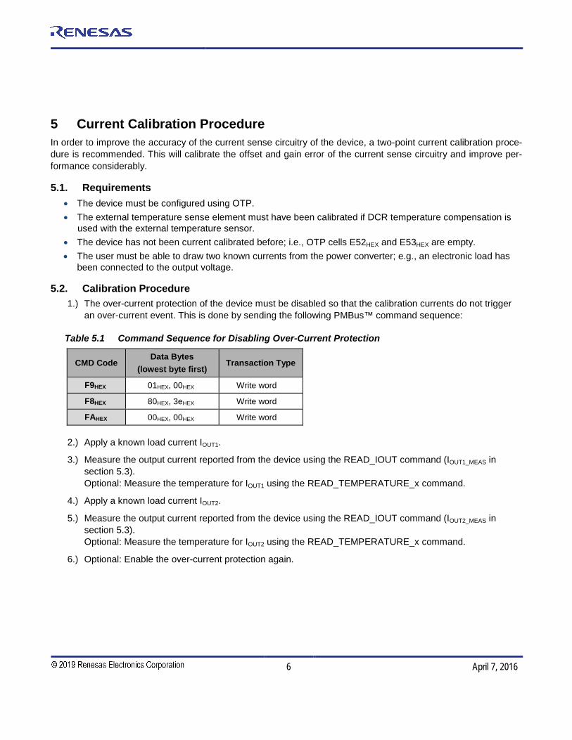
Table 5.1 Command Sequence for Disabling Over-Current Protection
CMD Code Data Bytes
(lowest byte first) Transaction Type
F9HEX 01HEX, 00HEX Write word
F8HEX 80HEX, 3eHEX Write word
FAHEX 00HEX, 00HEX Write word
2.) Apply a known load current IOUT1.
3.) Measure the output current reported from the device using the READ_IOUT command (IOUT1_MEAS in section 5.3). Optional: Measure the temperature for IOUT1 using the READ_TEMPERATURE_x command.
4.) Apply a known load current IOUT2.
5.) Measure the output current reported from the device using the READ_IOUT command (IOUT2_MEAS in section 5.3). Optional: Measure the temperature for IOUT2 using the READ_TEMPERATURE_x command.
6.) Optional: Enable the over-current protection again.

ZSPM1025A / ZSPM1035A Programming and Calibration
© 2016 Integrated Device Technology, Inc. 7 April 7, 2016
Table 5.2 Command Sequence for Re-enabling Over-Current Protection
CMD Code Data Bytes
(lowest byte first) Transaction Type
F9HEX 01HEX, 00HEX Write word
F8HEX 80HEX, 3eHEX Write word
FAHEX 80HEX, 00HEX Write word
7.) Compute the gain and offset correction factors according to the equations listed in the next section.
8.) Write gain and offset correction factors in the ZSPM10x5A. The gain factor is written into OTP cell E52HEX; the offset value is written into OTP cell E53HEX.
5.3. Computation of Current Sense Correction Factors The gain and offset correction factors can be computed from the nominal and measured current values using the following equations:
Gain correction factor: IOUT_CAL_GAIN_CORR = (IOUT2 - IOUT1) / (IOUT2_MEAS - IOUT1_MEAS)
Offset correction factor: IOUT_CAL_OFFSET = IOUT1 - (IOUT1_MEAS * ICOUT_CAL_GAIN_CORR)
Both values must be scaled prior to writing them into their respective OTP cells:
IOUT_CAL_GAIN_CORR_OTP = IOUT_CAL_GAIN_CORR * 128
IOUT_CAL_OFFSET_OTP = IOUT_CAL_OFFSET * IOUT_READ_FACTOR
IOUT_READ_FACTOR can be calculated from the content of OTP cell EF1HEX using the following equation:
IOUT_READ_FACTOR = OTP[EF1HEX] / 32.
Prior to writing the values into the OTP, the calibration values should be checked for correctness, as the values are constrained by the following limits:
Table 5.3 Limits for Calibration Values
Value Data Format Lower Limit Upper Limit
IOUT_CAL_GAIN_CORR_OTP Unsigned Q1.7 0.5 (0040HEX) 1.5 (00C0HEX)
IOUT_CAL_OFFSET_OTP Signed Q0.7, 16-bit signed extended -0.75 (FFA0HEX) 0.75 (0060HEX)
5.4. DCR Temperature Correction during Calibration If output current sensing is required with high accuracy or the temperature during calibration is significantly higher than 25°C, a correction of the DCR temperature rise is recommended during calibration. This is due to the fact that gain and offset of the current sense circuitry are defined for 25°C.
This temperature correction can be easily done by scaling the measured currents with the DCR temperature correction values.
ZSPM1025A / ZSPM1035A Programming and Calibration
© 2016 Integrated Device Technology, Inc. 8 April 7, 2016
The current information read with the READ_IOUT command is converted into the temperature-corrected current IOUT_TC_COR using
IOUT_TC_COR = READ_IOUT / (1.0 + TC_DCR * (T - 25))
Where
TC_DCR is the temperature coefficient of the DCR. T is the actual temperature during the measurement of the output current.
The temperature corrected currents are then substituted into the equations in section 5.3 instead of the actual uncorrected readings.
Recommendation: Read the temperature of the sensor configured for the DCR temperature correction algorithm in the device; i.e., READ_TEMPERATURE_1 if the external sensor is used and READ_TEMPERATURE_2 if the internal sensor is used.
The temperature coefficient of the DCR is set to 3900ppm/°C by default. Alternatively, it can be extracted from the device using the following equations:
If the external temperature sensor is used: TC_DCR = OTP[EF2HEX] / 16.0 / OTP[EEEHEX]
If the internal temperature sensor is used: TC_DCR = OTP[EF2HEX] / 16.0 / OTP[E47HEX]
Note that the OTP cells EF2HEX, EEEHEX and E47HEX are all in 16-bit signed data format.
5.5. Calculation Examples Scenario 1:
Assume this is a calibration of a power converter with a nominal current of IOUT1 = 5.0A and IOUT2 = 25A; the OTP[EF1HEX] = 19BHEX; and IOUT1_MEAS has been measured as 2.8A and IOUT2_MEAS as 19.7A.
Calculate the correction coefficients:
IOUT_CAL_GAIN_CORR = (25.0 – 5.0) / (19.7 – 2.8) = 1.18 IOUT_CAL_OFFSET = 5 – (2.8 * 1.18) = 1.70.
Convert this into OTP format as follows:
IOUT_CAL_GAIN_CORR_OTP = 1.18 * 128 = 151 = 0097HEX IOUT_CAL_OFFSET_OTP = 1.70 * (411 / 32) = 22 = 0016HEX
Both values lie within the allowed limits of the ZSPM10x5A and hence can be written into the IC.
Scenario 2:
Assume this is a calibration of a power converter with nominal current of IOUT1 = 5.0A and IOUT2 = 15A; the OTP[EF1HEX] = 19BHEX; and IOUT1_MEAS has been measured as 4.79 A and IOUT2_MEAS as 13.66 A. Calculate the correction coefficients:
IOUT_CAL_GAIN_CORR = (15.0 – 5.0) / (13.66 – 4.79) = 1.128 IOUT_CAL_OFFSET = 5 – (4.79 * 1.128) = -0.402.

ZSPM1025A / ZSPM1035A Programming and Calibration
© 2016 Integrated Device Technology, Inc. 9 April 7, 2016
Convert this into OTP format as follows:
IOUT_CAL_GAIN_CORR_OTP = 1.128 * 128 = 144 = 0090HEX IOUT_CAL_OFFSET_OTP = -0.402 * (411 / 32) = -5 = FFFBHEX
Both values lie within the allowed limits of the ZSPM10x5A and hence can be written into the IC.
Scenario 3:
Assume this is a calibration of a power converter with nominal current of IOUT1 = 5.0A and IOUT2 = 20A; IOUT1_MEAS has been measured as 4.96 A at 31.0°C and IOUT2_MEAS as 18.24 A at 31.0°C. The OTP contains these values: OTP[EEEHEX] = FD70HEX, OTP[EF1HEX] = 019BHEX and OTP[EF2HEX] = FFD2HEX. The external temperature sensor is used for DCR compensation. The DCR temperature coefficients is calculated as
TC_DCR = -41 / 16.0 / -655 = 0.0039
Next the current measurements are temperature corrected: IOUT1_TC_COR = 4.96 / (1.0 + 0.0039 * (31.0 – 25.0)) = 4.84
IOUT1_TC_COR = 18.24 / (1.0 + 0.0039 * (31.0 – 25.0)) = 17.82
Substituting these values into the equations gives
IOUT_CAL_GAIN_CORR = (20.0 – 5.0) / (17.82 – 4.84) = 1.156 IOUT_CAL_OFFSET = 5 – (4.84 * 1.156) = -0.600.
Convert this into OTP format as follows:
IOUT_CAL_GAIN_CORR_OTP = 1.156 * 128 = 148 = 0094HEX IOUT_CAL_OFFSET_OTP = -0.600 * (411 / 32) = -8 = FFF8HEX
Both values lie within the allowed limits of the ZSPM10x5A and hence can be written into the IC.
ZSPM1025A / ZSPM1035A Programming and Calibration
© 2016 Integrated Device Technology, Inc. 10 April 7, 2016
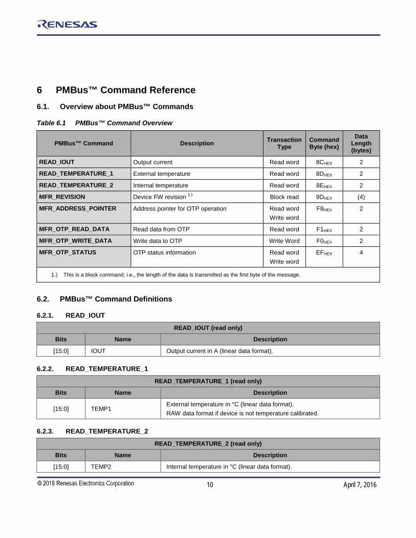
6 PMBus™ Command Reference 6.1. Overview about PMBus™ Commands
Table 6.1 PMBus™ Command Overview
PMBus™ Command Description Transaction Type
Command Byte (hex)
Data Length (bytes)
READ_IOUT Output current Read word 8CHEX 2
READ_TEMPERATURE_1 External temperature Read word 8DHEX 2
READ_TEMPERATURE_2 Internal temperature Read word 8EHEX 2
MFR_REVISION Device FW revision 1.) Block read 9DHEX (4)
MFR_ADDRESS_POINTER Address pointer for OTP operation Read word Write word
F8HEX 2
MFR_OTP_READ_DATA Read data from OTP Read word F1HEX 2
MFR_OTP_WRITE_DATA Write data to OTP Write Word F0HEX 2
MFR_OTP_STATUS OTP status information Read word Write word
EFHEX 4
1.) This is a block command; i.e., the length of the data is transmitted as the first byte of the message.
6.2. PMBus™ Command Definitions
6.2.1. READ_IOUT
READ_IOUT (read only)
Bits Name Description
[15:0] IOUT Output current in A (linear data format).
6.2.2. READ_TEMPERATURE_1
READ_TEMPERATURE_1 (read only)
Bits Name Description
[15:0] TEMP1 External temperature in °C (linear data format). RAW data format if device is not temperature calibrated.
6.2.3. READ_TEMPERATURE_2
READ_TEMPERATURE_2 (read only)
Bits Name Description
[15:0] TEMP2 Internal temperature in °C (linear data format).
ZSPM1025A / ZSPM1035A Programming and Calibration
© 2016 Integrated Device Technology, Inc. 11 April 7, 2016
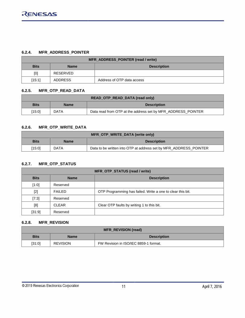
6.2.4. MFR_ADDRESS_POINTER
MFR_ADDRESS_POINTER (read / write)
Bits Name Description
[0] RESERVED
[15:1] ADDRESS Address of OTP data access
6.2.5. MFR_OTP_READ_DATA
READ_OTP_READ_DATA (read only)
Bits Name Description
[15:0] DATA Data read from OTP at the address set by MFR_ADDRESS_POINTER
6.2.6. MFR_OTP_WRITE_DATA
MFR_OTP_WRITE_DATA (write only)
Bits Name Description
[15:0] DATA Data to be written into OTP at address set by MFR_ADDRESS_POINTER
6.2.7. MFR_OTP_STATUS
MFR_OTP_STATUS (read / write)
Bits Name Description
[1:0] Reserved
[2] FAILED OTP Programming has failed. Write a one to clear this bit.
[7:3] Reserved
[8] CLEAR Clear OTP faults by writing 1 to this bit.
[31:9] Reserved
6.2.8. MFR_REVISION
MFR_REVISION (read)
Bits Name Description
[31:0] REVISION FW Revision in ISO/IEC 8859-1 format.
ZSPM1025A / ZSPM1035A Programming and Calibration
© 2016 Integrated Device Technology, Inc. 12 April 7, 2016
7 Related Documents
Document
ZSPM1025A Data Sheet
ZSPM1035A Data Sheet
ZSPM8025-KIT Evaluation Kit Description
ZSPM8035-KIT Evaluation Kit Description
Pink Power Designer™ Graphic User Interface (GUI)
Visit www.IDT.com/ZSPM1025A, www.IDT.com/ZSPM1035A, www.IDT.com/ZSPM8025-KIT, www.IDT.com/ZSPM8035-KIT or contact your nearest sales office for the latest version of these documents.
8 Document Revision History Revision Date Description
1.00 October 22, 2013 First release.
April 7, 2016 Changed to IDT branding.
Corporate Headquarters 6024 Silver Creek Valley Road San Jose, CA 95138 www.IDT.com
Sales 1-800-345-7015 or 408-284-8200Fax: 408-284-2775www.IDT.com/go/sales
Tech Support www.IDT.com/go/support
DISCLAIMER Integrated Device Technology, Inc. (IDT) reserves the right to modify the products and/or specifications described herein at any time, without notice, at IDT's sole discretion. Performance specifications and operating parameters of the described products are determined in an independent state and are not guaranteed to perform the same way when installed in customer products. The information contained herein is provided without representation or warranty of any kind, whether express or implied, including, but not limited to, the suitability of IDT's products for any particular purpose, an implied warranty of merchantability, or non-infringement of the intellectual property rights of others. This document is presented only as a guide and does not convey any license under intellectual property rights of IDT or any third parties.
IDT's products are not intended for use in applications involving extreme environmental conditions or in life support systems or similar devices where the failure or malfunction of an IDT product can be reasonably expected to significantly affect the health or safety of users. Anyone using an IDT product in such a manner does so at their own risk, absent an express, written agreement by IDT.
Integrated Device Technology, IDT and the IDT logo are trademarks or registered trademarks of IDT and its subsidiaries in the United States and other countries. Other trademarks used herein are the property of IDT or their respective third party owners. For datasheet type definitions and a glossary of common terms, visit www.idt.com/go/glossary. All contents of this document are copyright of Integrated Device Technology, Inc. All rights reserved.

Corporate HeadquartersTOYOSU FORESIA, 3-2-24 Toyosu,Koto-ku, Tokyo 135-0061, Japanwww.renesas.com
Contact InformationFor further information on a product, technology, the most up-to-date version of a document, or your nearest sales office, please visit:www.renesas.com/contact/
TrademarksRenesas and the Renesas logo are trademarks of Renesas Electronics Corporation. All trademarks and registered trademarks are the property of their respective owners.
IMPORTANT NOTICE AND DISCLAIMER
RENESAS ELECTRONICS CORPORATION AND ITS SUBSIDIARIES (“RENESAS”) PROVIDES TECHNICAL SPECIFICATIONS AND RELIABILITY DATA (INCLUDING DATASHEETS), DESIGN RESOURCES (INCLUDING REFERENCE DESIGNS), APPLICATION OR OTHER DESIGN ADVICE, WEB TOOLS, SAFETY INFORMATION, AND OTHER RESOURCES “AS IS” AND WITH ALL FAULTS, AND DISCLAIMS ALL WARRANTIES, EXPRESS OR IMPLIED, INCLUDING, WITHOUT LIMITATION, ANY IMPLIED WARRANTIES OF MERCHANTABILITY, FITNESS FOR A PARTICULAR PURPOSE, OR NON-INFRINGEMENT OF THIRD PARTY INTELLECTUAL PROPERTY RIGHTS.
These resources are intended for developers skilled in the art designing with Renesas products. You are solely responsible for (1) selecting the appropriate products for your application, (2) designing, validating, and testing your application, and (3) ensuring your application meets applicable standards, and any other safety, security, or other requirements. These resources are subject to change without notice. Renesas grants you permission to use these resources only for development of an application that uses Renesas products. Other reproduction or use of these resources is strictly prohibited. No license is granted to any other Renesas intellectual property or to any third party intellectual property. Renesas disclaims responsibility for, and you will fully indemnify Renesas and its representatives against, any claims, damages, costs, losses, or liabilities arising out of your use of these resources. Renesas' products are provided only subject to Renesas' Terms and Conditions of Sale or other applicable terms agreed to in writing. No use of any Renesas resources expands or otherwise alters any applicable warranties or warranty disclaimers for these products.
(Rev.1.0 Mar 2020)
© 2020 Renesas Electronics Corporation. All rights reserved.


![STCS B - mecalbi.com · Power Line and Hot Air Programming Interface SHRINKING CHAMBER Shrinking Chamber CALIBRATION Calibration Probe 150 [ºC] 350 [ºC] (Due to material limitations,](https://img.pdfslide.net/doc/110x75/5c7fd14009d3f257328bdf6c/stcs-b-power-line-and-hot-air-programming-interface-shrinking-chamber-shrinking.jpg)