Embed Size (px)
Citation preview
ZXBM1021 Document number: DS36322 Rev. 2 - 2
1 of 25 www.diodes.com
April 2014 © Diodes Incorporated
ZXBM1021
SINGLE PHASE VARIABLE SPEED MOTOR CONTROL PRE-DRIVER
Description
The ZXBM1021 is a high performance, low noise, single-phase,
Direct Current Brushless (BLDC) motor pre-driver with variable PWM
speed control and current control suitable for fan and blower motors.
For system flexibility the motor speed can be controlled by either an
external PWM control signal or by a DC voltage signal from an
external control voltage or from a Thermistor network.
To prevent motor inrush current the device has a soft start feature. To
help protect the motor coil, the ZXBM1021 provides rotor lock
protection which shuts down the output drive if rotor lock is detected.
The device automatically re-starts with soft-start when the rotor lock is
removed. The ZXBM1021 monitors the motor current to provide a
programmable over current limit.
A Tachometer output is provided by the open collector output
Frequency Generator (FG) pin which allows external interface to
monitor motor rotation or speed. The FG output is the magnetic
change frequency.
The ZXBM1021 is available in space saving and low profile
U-QFN4040-20 and industry standard QSOP-20 packages.
Features
Operating voltage: 6.8V to 18V
Can be extended with external regulator
Speed control via external PWM, DC or Thermistor signals
Low noise, high efficiency
Soft start
Integrated current control
Reference voltage output
Built-in Hall amplifier for direct connection of Hall element
Rotor Lock Protection
Lock detection, output shutdown and automatic re-start
Minimum speed setting
Frequency generator (FG) output
Thermally enhanced space saving low profile U-QFN4040-20 and
industry standard QSOP-20 packages
Totally Lead-Free & Fully RoHS Compliant (Notes 1 & 2)
Halogen and Antimony Free. “Green” Device (Note 3)
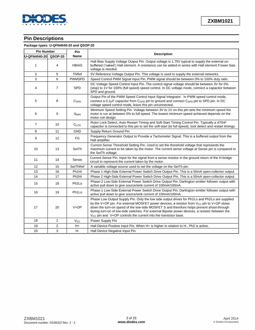
Pin Assignments
(Top View)
VC
C
H+
ThRef
PWMSPD
CSPD
CL
CK
Ph2
Hi
H-
SPD
SM
IN FG
Ph1Lo
Ph2Lo
Ph1Hi
SetThRef
Sense
Se
tTh
GN
D
V+
OP
HBIAS
ZXBM1021
U-QFN4040-20
(Top View)
H+
SetThRef
SPD
H-
GND
Ph1Lo
Ph2Lo
CSPD
CLCK
FG
ThRef
SMIN
1
Ph1Hi
Ph2Hi
Sense
SetTh
V+OPVcc
PWMSPD
20
10 11
HBIAS
ZXBM1021
QSOP-20
Applications
Personal, servers and mainframe computers cooling fans
Instrumentation and equipment cooling fans
Home appliance fans and blowers
Central heating blowers and extraction systems
Industrial fans, blower and extractors
Hand dryers
Hand-held power tools
Pumps
Notes: 1. No purposely added lead. Fully EU Directive 2002/95/EC (RoHS) & 2011/65/EU (RoHS 2) compliant. 2. See http://www.diodes.com/quality/lead_free.html for more information about Diodes Incorporated’s definitions of Halogen- and Antimony-free, "Green" and Lead-free. 3. Halogen- and Antimony-free "Green” products are defined as those which contain <900ppm bromine, <900ppm chlorine (<1500ppm total Br + Cl) and <1000ppm antimony compounds.

ZXBM1021 Document number: DS36322 Rev. 2 - 2
2 of 25 www.diodes.com
April 2014 © Diodes Incorporated
ZXBM1021
Typical Applications Circuit (Note 4)
ZXBM1021
VCC
H+
H-
CLCK
SPD
C3
C2
C11µF
0.1uF
0.47µF
0V
FG
Typical Applications Circuit for PWM Control
using the ZXBM1021 and ZXMC MOSFET 1/2 Bridge Drivers
ThRef
SMIN
Ph1Lo
Ph2Lo
GND
Q1-4
W1
470Ω
R2470Ω
ZXMC
3A17DN8
FG
Ph1Hi
Ph2Hi
R1
R5
R3
R4R6
100Ω
100Ω
1kΩ 1kΩ
C5
2.2µF
12V
D11N4148
D2
1N4004
SetTh
Sense
PWM control
R10
16kΩ
R9
12kΩ
Hall
R8470Ω
R733kΩ
Rsense0.1Ω
3 3
4 4
5 & 6 5 & 6
7 & 8 7 & 8
2 2
1 1
SetThRefPWMSPD
CSPD
0.1µF
C4
V+OP
HBIAS
R12
(Optional)
ZXBM1021
VCC
H+
H-
CLCK
SPD
C3
C2
C11µF
0.1uF
0.47µF
0V
FG
Typical Applications Circuit for DC Control
using the ZXBM1021 and ZXMC MOSFET 1/2 Bridge Drivers
ThRef
SMIN
Ph1Lo
Ph2Lo
Gnd
Q1-4
W1
470Ω
R2470Ω
ZXMC
3A17DN8
FG
Ph1Hi
Ph2Hi
R1
R5
R3
R4R6
100Ω
100Ω
1kΩ 1kΩ
C5
2.2µF
12V
D1 1N4148
D2
1N4004
SetTh
Sense
R10
16kΩ
R9
12kΩ
Hall
R8470Ω
R733kΩ
Rsense0.1Ω
3 3
4 4
5 & 6 5 & 6
7 & 8 7 & 8
2 2
1 1
SetThRefPWMSPD
CSPD
0.1µF
C4
V+OP
HBIAS
DC control
R1110kΩ
R12
(Optional)
Note: 4. FG pull-up resistor is not shown in the typical application circuit. Generally, the FG pull-up resistor is located at the system host end rather than the fan motor PCB.
ZXBM1021 Document number: DS36322 Rev. 2 - 2
3 of 25 www.diodes.com
April 2014 © Diodes Incorporated
ZXBM1021
Pin Descriptions
Package types: U-QFN4040-20 and QSOP-20
Pin Number Pin
Name Description
U-QFN4040-20 QSOP-20
1 4 HBIAS Hall Bias Supply Voltage Output Pin. Output voltage is 1.75V typical to supply the external un-buffered (‘naked’) Hall element. A resistance can be added in series with Hall element if lower bias voltage is needed.
2 5 ThRef 5V Reference Voltage Output Pin. This voltage is used to supply the external networks.
3 6 PWMSPD Speed Control PWM Signal Input Pin. PWM signal should be between 0% to 100% duty ratio.
4 7 SPD DC Voltage Speed Control Input Pin. The control signal voltage should be between 3V for 0% (stop) to 1V for 100% (full speed) speed control. In DC voltage mode, connect a capacitor between SPD and ground.
5 8 CSPD
Output Pin of the PWM Speed Control Input Signal Integrator. In PWM speed control mode,
connect a 0.1F capacitor from CSPD pin to ground and connect CSPD pin to SPD pin. In DC voltage speed control mode, leave this pin unconnected.
6 9 SMIN
Minimum Speed Setting Pin. Voltage between 3V to 1V on this pin sets the minimum speed the motor is run at between 0% to full speed. The lowest minimum speed achieved depends on the motor coil design.
7 10 CLCK Rotor Lock Detect, Auto Restart Timing and Soft-Start Timing Control Pin. Typically a 470nF capacitor is connected to this pin to set the soft-start (to full speed), lock detect and restart timings.
8 11 GND Supply Return Ground Pin
9 12 FG Frequency Generator Output to Provide a Tachometer Signal. This is a buffered output from the Hall amplifier.
10 13 SetTh Current Sense Threshold Setting Pin. Used to set the threshold voltage that represents the maximum current to be taken by the motor. The current sense voltage at Sense pin is compared to the SetTh voltage.
11 14 Sense Current Sense Pin. Input for the signal from a sense resistor in the ground return of the H-bridge circuit to represent the current taken by the motor.
12 15 SetThRef A variable voltage source used to set the voltage on the SetTh pin.
13 16 Ph1Hi Phase 1 High-Side External Power Switch Drive Output Pin. This is a 50mA open-collector output.
14 17 Ph2Hi Phase 2 High-Side External Power Switch Drive Output Pin. This is a 50mA open-collector output.
15 18 Ph2Lo Phase-2 Low-Side External Power Switch Drive Output Pin. Darlington emitter follower output with active pull down to give source/sink current of 100mA/100mA.
16 19 Ph1Lo Phase-1 Low-Side External Power Switch Drive Output Pin. Darlington emitter follower output with active pull down to give source/sink current of 100mA/100mA.
17 20 V+OP
Phase Low Output Supply Pin. Only the low side output drives for Ph1Lo and Ph2Lo are supplied
by the V+OP pin. For external MOSFET power devices, a resistor from VCC pin to V+OP slows
down the turn-on speed of the low-side MOSFET S and therefore helps prevent shoot-through during turn-on of low-side switches. For external Bipolar power devices, a resistor between the
VCC pin and V+OP controls the current into the transistor base.
18 1 VCC Power Supply Pin
19 2 H+ Hall Device Positive Input Pin. When H+ is higher in relation to H-, Ph2 is active.
20 3 H- Hall Device Negative Input Pin

ZXBM1021 Document number: DS36322 Rev. 2 - 2
4 of 25 www.diodes.com
April 2014 © Diodes Incorporated
ZXBM1021
Functional Block Diagram (Note 5)
Speed &
Lock
Detect
Hall
FG
CLCK
SPD
H+
H-Hall
Amp
PWM
Integrator
Locked
Rotor
Detect
Phase
Drive &
Control
Gnd
Vcc
Set Min
Speed
Vref
SMIN
ThRef
Ph2 Lo
Ph1 Lo
Ph2 Hi
Ph1 Hi
Vcc
Vcc
Phase
Drive
Current
Monitor SetTh
Sense
Voltage Speed Control
VSPD Vcc
Vcc
Hall
Bias
HBIAS
Start-up
SetThRef
PWMSPD
PWM speed control
PWMSPD
CSPD
D2
RD
V+OP
PWM Osc
Note: 5. The ZXBM1021 has an open-collector FG. Typically a pull-up resistor of 10kΩ is recommended from FG pin to the supply voltage.
ZXBM1021 Document number: DS36322 Rev. 2 - 2
5 of 25 www.diodes.com
April 2014 © Diodes Incorporated
ZXBM1021
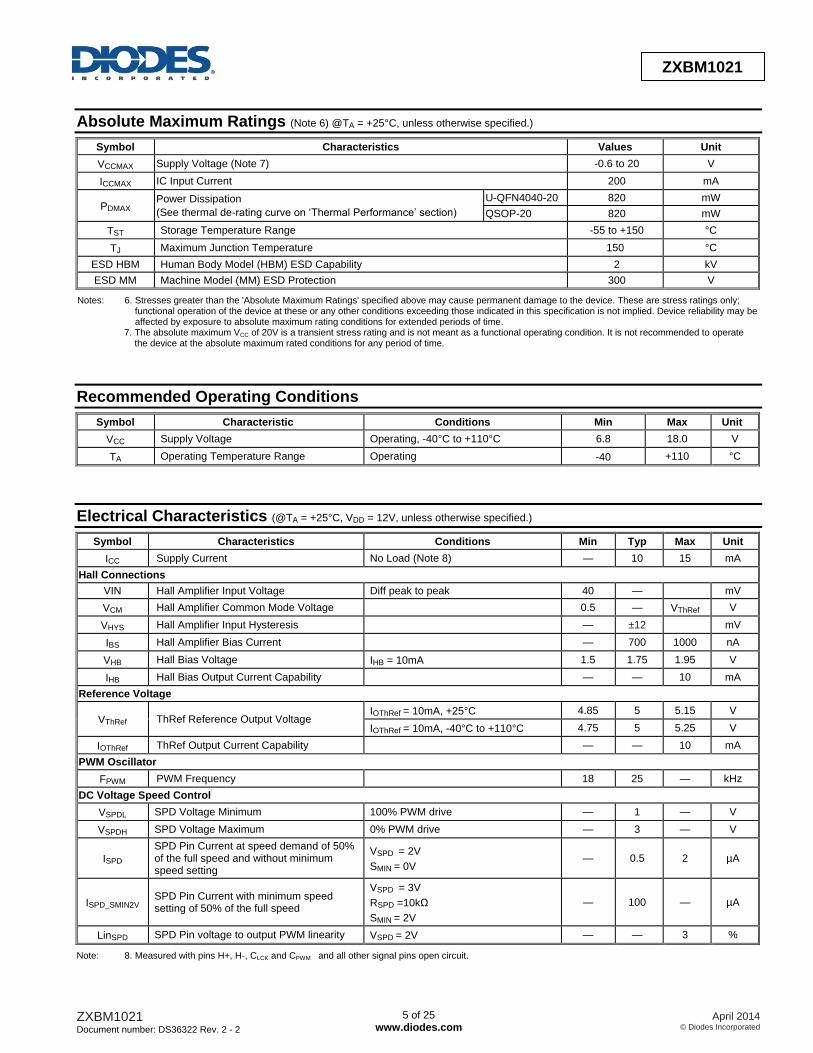
Absolute Maximum Ratings (Note 6) @TA = +25°C, unless otherwise specified.)
Symbol Characteristics Values Unit
VCCMAX Supply Voltage (Note 7) -0.6 to 20 V
ICCMAX IC Input Current 200 mA
PDMAX Power Dissipation
(See thermal de-rating curve on ‘Thermal Performance’ section)
U-QFN4040-20 820 mW
QSOP-20 820 mW
TST Storage Temperature Range -55 to +150 °C
TJ Maximum Junction Temperature 150 °C
ESD HBM Human Body Model (HBM) ESD Capability 2 kV
ESD MM Machine Model (MM) ESD Protection 300 V
Notes: 6. Stresses greater than the 'Absolute Maximum Ratings' specified above may cause permanent damage to the device. These are stress ratings only; functional operation of the device at these or any other conditions exceeding those indicated in this specification is not implied. Device reliability may be affected by exposure to absolute maximum rating conditions for extended periods of time. 7. The absolute maximum VCC of 20V is a transient stress rating and is not meant as a functional operating condition. It is not recommended to operate the device at the absolute maximum rated conditions for any period of time.
Recommended Operating Conditions
Symbol Characteristic Conditions Min Max Unit
VCC Supply Voltage Operating, -40°C to +110°C 6.8 18.0 V
TA Operating Temperature Range Operating -40 +110 °C
Electrical Characteristics (@TA = +25°C, VDD = 12V, unless otherwise specified.)
Symbol Characteristics Conditions Min Typ Max Unit
ICC Supply Current No Load (Note 8) — 10 15 mA
Hall Connections
VIN Hall Amplifier Input Voltage Diff peak to peak 40 — mV
VCM Hall Amplifier Common Mode Voltage 0.5 — VThRef V
VHYS Hall Amplifier Input Hysteresis — ±12 mV
IBS Hall Amplifier Bias Current — 700 1000 nA
VHB Hall Bias Voltage IHB = 10mA 1.5 1.75 1.95 V
IHB Hall Bias Output Current Capability — — 10 mA
Reference Voltage
VThRef ThRef Reference Output Voltage IOThRef = 10mA, +25°C 4.85 5 5.15 V
IOThRef = 10mA, -40°C to +110°C 4.75 5 5.25 V
IOThRef ThRef Output Current Capability — — 10 mA
PWM Oscillator
FPWM PWM Frequency 18 25 — kHz
DC Voltage Speed Control
VSPDL SPD Voltage Minimum 100% PWM drive — 1 — V
VSPDH SPD Voltage Maximum 0% PWM drive — 3 — V
ISPD
SPD Pin Current at speed demand of 50% of the full speed and without minimum speed setting
VSPD = 2V
SMIN = 0V — 0.5 2 µA
ISPD_SMIN2V SPD Pin Current with minimum speed setting of 50% of the full speed
VSPD = 3V
RSPD =10kΩ
SMIN = 2V
— 100 — µA
LinSPD SPD Pin voltage to output PWM linearity VSPD = 2V — — 3 %
Note: 8. Measured with pins H+, H-, CLCK and CPWM and all other signal pins open circuit.

ZXBM1021 Document number: DS36322 Rev. 2 - 2
6 of 25 www.diodes.com
April 2014 © Diodes Incorporated
ZXBM1021
Electrical Characteristics (cont.) (@TA = +25°C, VDD = 12V, unless otherwise specified.)
Symbol Characteristics Conditions Min Typ Max Unit
PWM Speed Control
VPWMSPDH PWMSPD High Level 2 VCC V
VPWMSPDL PWMSPD Low Level 0.4 V
IPWMSPD PWMSPD High Level Input Current 0.8 2 µA
DPWMSPD PWM Speed Signal Duty Range 0 100 %
FPWM_MAX Maximum Frequency of PWM Control Signal 100 kHz
LinINT PWMSPD Pin PWM Duty Ratio to CSPD Output Voltage Linearity
PWMSPD duty ratio 50%,
PWM frequency FPWM = 25kHz 1.94 2 2.06 V
Minimum Speed Setting
ISMIN SMIN Input Current VSMIN = 2V -0.25 -0.5 µA
Soft Start
tSS Soft-Start Time to Full Speed CLCK = 0.47µF 3 s
Lock Timing
Lock Condition TLCKDET : TOFF ratio 1:8
ILCKCL CLCK Charge Current – Soft Start (from lock) and in Lock Mode
Lock mode,
VCLCK = 2.5V 0.45 0.7 1.07 µA
ILCKCR CLCK Charge Current – Run Run mode 3.25 5.5 9.0 µA
ILCKDL CLCK Discharge Current - Lock Lock mode,
VCLCK = 2.5V 0.45 0.7 1.07 µA
VCLCKTHH CLCK High Threshold Voltage 5 V
VCLCKTHL CLCK Low Threshold Voltage Lock mode 0.6 V
Current Limit
VSetThRef SetThRef Output Voltage ISetThRef = 200uA ThRef-
0.17
ThRef-
0.1V
ThRef-
0.05 V
ISetThRef SetThRef Output Current -200 µA
ISENSE Sense Input Current -20 -100 nA
ISetTh SetTh Input Current -20 -100 nA
Output Drives
VOH Ph1Lo and Ph2Lo Output High Voltage IOH = 100mA VCC - 2.2 VCC - 1.7 V
VOLA Ph1Lo and Ph2Lo Output Low Voltage IOL =100mA (Note 9) 0.3 0.5 V
VOLB Ph1Lo and Ph2Lo Output Low Voltage IOH = 50µA (Note 10) 0.3 0.5 V
IOH Ph1Lo and Ph2Lo Output Source Current 100 mA
IOL Ph1Lo and Ph2Lo Output Sink Current 100 mA
VOLA Ph1Hi and Ph2Hi Output Low Voltage IOH =50mA (Note 10) 0.3 0.5 V
IOL Ph1Hi and Ph2Hi Output Sink Current 50 mA
IOFF Ph1Hi and Ph2Hi Off Output Leakage Current ±100 nA
tCD Commutation Delay 20 70 µs
Output Flags
IFGOL FG Low Level Output Current Capability 10 mA
VFGOL FG Low Level Output Voltage IFGOL = 10mA 0.4 V
Lock Conditions
TLCKDET
Lock Detect Time (time it waits for before next Hall signal before deciding to turn outputs off for fixed time)
CLCK =0.47µF
ILCKCR = 5.5µA 400 ms
TOFF Output Off Time after lock is detected. CLCK =0.47µF 3 s
Notes: 9. Measured when opposing Phase Output is Low. 10. Measured when opposing Phase Output is High.

ZXBM1021 Document number: DS36322 Rev. 2 - 2
7 of 25 www.diodes.com
April 2014 © Diodes Incorporated
ZXBM1021
Functional Descriptions
H-Bias – Hall Bias Output
This is a 1.75V nominal voltage source to bias a differential un-buffered Hall element sensor. If a Hall element requires a lower voltage than the
H-Bias output, connect an appropriate value resistor between the H-Bias pin and the Hall element supply pin.
H+ and H- – Hall Inputs
The rotor position is detected by a Hall sensor, with the output applied to the H+ and H-pins. This sensor can be either a 4 pin 'naked' Hall device
or of the 3 pin buffered switching type. For a 4 pin device the differential Hall output signal is connected to the H+ and H- pins. For a buffered Hall
sensor the Hall device output is attached to the H+ pin, with a pull-up attached if needed, whilst the H- pin has an external potential divider
attached to hold the pin at half VThRef. When H+ is high in relation to H-, Ph2 is the active drive.
ThRef – Output Reference Voltage
This is a 5V nominal reference output voltage. It is designed to 'source' current and therefore it will not 'sink' any current from a higher voltage.
The total current drawn from the ThRef pin by any external circuitry, such as the minimum speed potential divider to SMIN pin, should not exceed
10mA.
SPD –Speed Control DC Voltage Input
The voltage applied to the SPD pin provides control over the fan motor speed by varying the Pulse Width Modulated (PWM) drive ratio at the
Ph1Lo and Ph2Lo outputs. The control signal takes the form of a variable DC voltage input of range 3V to 1V, representing 0% to 100% drive
respectively.
If variable speed control is not required this pin can be tied to an external potential divider to set a fixed speed or tied to ground to provide full
speed i.e. 100% PWM drive.
If required this pin can also be used as an enable pin. The application of a voltage >3.0V on this pin will force the PWM drive fully off, in effect
disabling the drive, providing the minimum speed function is not active (see SMIN pin section below).
1 in typical
application circuit for DC control in page 2) between speed control DC voltage input source and SPD pin.
PWMSPD – Speed Control PWM Signal Input
The duty ratio of the speed control PWM signal input to this pin controls the fan motor speed by varying the output drive PWM ratio at the Ph1Lo
and Ph2Lo outputs. In the PWM speed control mode, the PWMSPD pin and the CSPD pin work together to the control the speed. The PWM
signal input on the PWMSPD pin is integrated by the capacitor on the CSPD pin (See CSPD pin description). PWM control input signal to the
PWMSPD pin needs to be a TTL logic levels.
CSPD – PWM Speed Control Signal Integrator Output
When PWM input signal is used to control the motor speed, PWM signal is integrated to DC voltage between 1V to 3V to for speed control. If
PWMSPD pin input is TTL low, the output voltage on CSPD is 3V and if PWMSPD pin is TTL high, the CSPD pin output is at 1V. In order for the
nput PWM frequency
applied to the PWMSPD input.
In PWM speed control mode, SPD pin to ground and connect CSPD pin to SPD pin. When in DC voltage speed
control mode keep PWMSPD and CSPD pins unconnected.
SMIN – Minimum Speed Setting
A voltage can be set on this pin via a potential divider between the ThRef and GND pins. This voltage is monitored by the SPD pin to clamp the
SPD control voltage so that it does not rise above SMIN voltage. As a higher voltage on the SPD pin represents a lower speed, the SMIN setting
prevents the motor speed going lower than the minimum speed set by the SMIN pin. If this feature is not required the pin is left tied to ThRef so no
minimum speed will be set.
If the fan is being controlled from an external voltage source onto the SPD pin then either this feature should not be used or if the minimum
ZXBM1021 Document number: DS36322 Rev. 2 - 2
8 of 25 www.diodes.com
April 2014 © Diodes Incorporated
ZXBM1021
Functional Descriptions (cont.)
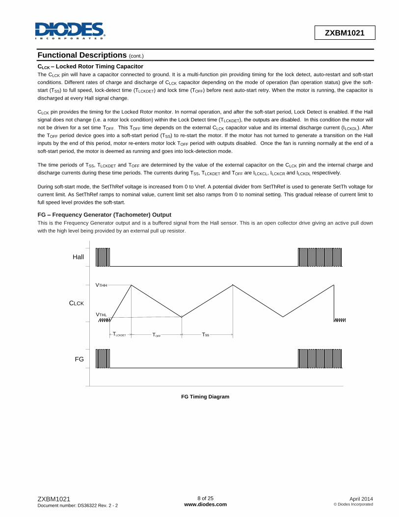
CLCK – Locked Rotor Timing Capacitor
The CLCK pin will have a capacitor connected to ground. It is a multi-function pin providing timing for the lock detect, auto-restart and soft-start
conditions. Different rates of charge and discharge of CLCK capacitor depending on the mode of operation (fan operation status) give the soft-
start (TSS) to full speed, lock-detect time (TLCKDET) and lock time (TOFF) before next auto-start retry. When the motor is running, the capacitor is
discharged at every Hall signal change.
CLCK pin provides the timing for the Locked Rotor monitor. In normal operation, and after the soft-start period, Lock Detect is enabled. If the Hall
signal does not change (i.e. a rotor lock condition) within the Lock Detect time (TLCKDET), the outputs are disabled. In this condition the motor will
not be driven for a set time TOFF. This TOFF time depends on the external CLCK capacitor value and its internal discharge current (ILCKDL). After
the TOFF period device goes into a soft-start period (TSS) to re-start the motor. If the motor has not turned to generate a transition on the Hall
inputs by the end of this period, motor re-enters motor lock TOFF period with outputs disabled. Once the fan is running normally at the end of a
soft-start period, the motor is deemed as running and goes into lock-detection mode.
The time periods of TSS, TLCKDET and TOFF are determined by the value of the external capacitor on the CLCK pin and the internal charge and
discharge currents during these time periods. The currents during TSS, TLCKDET and TOFF are ILCKCL, ILCKCR and ILCKDL respectively.
During soft-start mode, the SetThRef voltage is increased from 0 to Vref. A potential divider from SetThRef is used to generate SetTh voltage for
current limit. As SetThRef ramps to nominal value, current limit set also ramps from 0 to nominal setting. This gradual release of current limit to
full speed level provides the soft-start.
FG – Frequency Generator (Tachometer) Output
This is the Frequency Generator output and is a buffered signal from the Hall sensor. This is an open collector drive giving an active pull down
with the high level being provided by an external pull up resistor.
TLCKDET TOFF Tss
Hall
CLCK
FG
VTHH
VTHL
FG Timing Diagram

ZXBM1021 Document number: DS36322 Rev. 2 - 2
9 of 25 www.diodes.com
April 2014 © Diodes Incorporated
ZXBM1021
Functional Descriptions (cont.)
Sense – Current Control Sense
This pin is used by the current sensing circuit to monitor the current taken by the motor windings. The signal comes from a sense resistor in the
low-side ground return of the external H-bridge driver.
SetTh – Current Control Threshold Voltage
This pin is used by the current sensing circuit as the reference voltage for the voltage on the sense pin to be compared against. If the voltage on
the sense pin starts to exceed the voltage set on this pin the current control circuitry starts to back off the output drive PWM duty and thus
reducing the current being supplied to the motor coil.
SetThRef – SetTh and Start-up Reference
This pin is derived from an internal start-up circuit and is used as the source voltage for the potential divider network attached to the SetTh pin.
Under running conditions this voltage will be typically ThRef-0.1V. However, during start up the voltage ramps up from 0V to ThRef-0.1V at a rate
determined by the capacitor on the CLCK pin giving a gradual release of current limit from 0 to nominal setting. ThRef-0.1V is equal to 4.9V
typical.
This low power pin is capable of supplying a maximum of 200µA. It should only be used to supply the potential divider network attached to the
SetTh pin.
Ph1Lo and Ph2Lo – Low-Side External H-Bridge Drive Output
Ph1Lo and Ph2Lo outputs drive the low side of the external power device H-bridge that in turn drives the single phase winding. These outputs
provide both the commutation and PWM waveforms. The outputs are active pull-up and active pull-down to help faster switching off when driving
MOSFET devices with a high gate capacitance. When in the high state the outputs will provide up to 100mA of drive into the base or gates of
external transistors as shown in the typical application circuit shown on the front page.
When in the low state the active phase drive is again capable of sinking up to 100mA to aid turn off times during PWM operation. When the
phase is inactive the output is held low by a 7.5kΩ internal pull-down resistor.
Ph1Hi and Ph2Hi – High-Side External H-Bridge Driver
Ph1Hi and Ph2Hi are the high side outputs to the external H-bridge and are open collector outputs capable of sinking 50mA. This signal provides
commutation only to the H-bridge.
V+OP – Phase Outputs Supply Voltage
This pin is the supply to the Phase outputs Ph1Lo and Ph2Lo only. This pin can be connected to VCC pin directly or through a resistor. For
external Bipolar power devices the resistor on V+OP is used to control the current into the transistor base and its value is chosen accordingly.
For external MOSFET power devices, the pin can be used to slow down the turn-on speed of the low-side MOSFETS. Slowing down the turn-on
speed of low side switches helps to prevent parasitic turn-on of the high-side switches and thus helping to prevent shoot-through during turn-on
of low-side switches. The gate resistor connected at Ph1Lo and Ph2Lo plus the resistor on V+OP controls the turn on speed of the MOSFET.
The turn-off of speed of the MOSFETS is controlled by the gate resistor only.
VCC – IC Supply voltage This provides the supply for the device's internal circuitry except Ph1Lo and Ph2Lo output stages, which are supplied from the V+OP pin.
For 12V fans this can be supplied directly from the Fan Motor supply. For fans likely to run in excess of the 18V maximum rating for the device
this will be supplied from an external regulator such as a Zener diode or low drop out regulator.
GND – Supply Return This is the device supply ground return pin and will generally be the most negative supply pin to the fan.
ZXBM1021 Document number: DS36322 Rev. 2 - 2
10 of 25 www.diodes.com
April 2014 © Diodes Incorporated
ZXBM1021
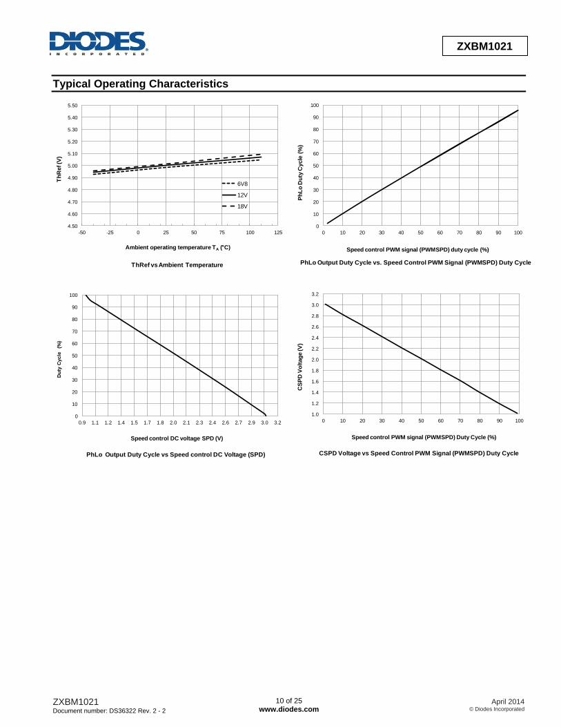
Typical Operating Characteristics
4.50
4.60
4.70
4.80
4.90
5.00
5.10
5.20
5.30
5.40
5.50
-50 -25 0 25 50 75 100 125
Th
Ref (V
)
Ambient operating temperature TA ( C)
ThRef vs Ambient Temperature
6V8
12V
18V
0
10
20
30
40
50
60
70
80
90
100
0 10 20 30 40 50 60 70 80 90 100
Ph
Lo
Du
ty C
ycle
(%
)
Speed control PWM signal (PWMSPD) duty cycle (%)
PhLo Output Duty Cycle vs. Speed Control PWM Signal (PWMSPD) Duty Cycle
0
10
20
30
40
50
60
70
80
90
100
0.9 1.1 1.2 1.4 1.5 1.7 1.8 2.0 2.1 2.3 2.4 2.6 2.7 2.9 3.0 3.2
Du
ty C
ycle
(%
)
Speed control DC voltage SPD (V)
PhLo Output Duty Cycle vs Speed control DC Voltage (SPD)
1.0
1.2
1.4
1.6
1.8
2.0
2.2
2.4
2.6
2.8
3.0
3.2
0 10 20 30 40 50 60 70 80 90 100
CS
PD
Vo
ltag
e (V
)
Speed control PWM signal (PWMSPD) Duty Cycle (%)
CSPD Voltage vs Speed Control PWM Signal (PWMSPD) Duty Cycle

ZXBM1021 Document number: DS36322 Rev. 2 - 2
11 of 25 www.diodes.com
April 2014 © Diodes Incorporated
ZXBM1021
Application Information
The ZXBM1021 is primarily controlled by a voltage on the SPD pin or a PWM signal on the PWMSPD pin.
A voltage of 1V represents a 100% PWM at the Phase Outputs and in turn represents full speed. 3V on the SPD pin conversely represents 0%
PWM. The motor can therefore be controlled simply by applying a control voltage onto the SPD pin with the minimal use of external components.
This voltage control method easily lends itself to control by other signal types. For example if a thermistor is applied to the SPD pin a varying
voltage can be generated at the SPD pin as the resistance of the thermistor varies with temperature.
A common form of control of fans is by a PWM signal derived from a central processor or controller. This speed control PWM signal can be
applied to PWMSPD pin. Motor speed is proportional to the duty ratio of the applied PWM speed control signal on PWMSPD pin.
Voltage on the SMIN pin sets the minimum speed of the motor. If the speed demand by either DC signal on SPD pin or PWM signal on PWMSPD
pin is lower than the minimum speed setting, motor will run at minimum speed.
The design of a motor system will be set around the maximum speed, the minimum speed and the current of the motor. The design of the motor
coil and the voltage on the output stage will set the maximum speed of the motor. The ZXBM1021 allows easy setting and control of the minimum speed and maximum motor current, as well as for controlling the speed.
DC Speed Control
The SPD pin will respond to an input DC voltage from 3V to 1V for 0% to 100% of the full speed. To allow internal minimum speed setting (SMIN)
and current control (ILIM) circuits to adjust the SPD pin voltage, the speed control DC voltage signal should be driven in via a 10kΩ series
resistor. The series resistor allows the SPD pin to vary even when driven externally by a low impedance source. A 0.1µF capacitor should be
connected from the SPD pin to supply ground.
When used in DC speed control mode, PWMSPD and CSPD pins should be left floating.
VC
C
H+
ThRef
PWMSPD
CSPD
CL
CK
Ph
2H
i
H-
SPD
SM
IN
FG
Ph1Lo
Ph2Lo
Ph1Hi
SetThRef
Sense
Se
tTh
GN
D
HBIAS
ZXBM1021
1
2
3
4
5
6 7 8 9 10
15
14
13
12
11
20 19 18 17 16
V+
OP
0.1µF
DC Speed Control
(3V to 1V)
R10kΩ
C
ZXBM1021 Document number: DS36322 Rev. 2 - 2
12 of 25 www.diodes.com
April 2014 © Diodes Incorporated
ZXBM1021
Application Information (cont.)
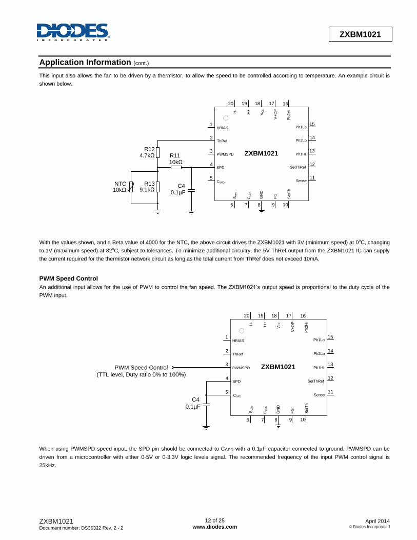
This input also allows the fan to be driven by a thermistor, to allow the speed to be controlled according to temperature. An example circuit is
shown below.
With the values shown, and a Beta value of 4000 for the NTC, the above circuit drives the ZXBM1021 with 3V (minimum speed) at 0oC, changing
to 1V (maximum speed) at 82oC, subject to tolerances. To minimize additional circuitry, the 5V ThRef output from the ZXBM1021 IC can supply
the current required for the thermistor network circuit as long as the total current from ThRef does not exceed 10mA.
PWM Speed Control
An additional input allows for the use of PWM to control the fan speed. The ZXBM1021’s output speed is proportional to the duty cycle of the
PWM input.
When using PWMSPD speed input, the SPD pin should be connected to CSPD with a 0.1F capacitor connected to ground. PWMSPD can be
driven from a microcontroller with either 0-5V or 0-3.3V logic levels signal. The recommended frequency of the input PWM control signal is
25kHz.
H+
ThRef
PWMSPD
Ph
2H
i
H-
SPD
FG
Ph1Lo
Ph2Lo
Ph1Hi
SetThRef
Sense
Se
tTh
GN
D
HBIAS
ZXBM1021
1
2
3
4
5
6 7 8 9 10
15
14
13
12
11
20 19 18 17 16
V+
OP
0.1µF
R1110kΩ
C4
R124.7kΩ
R139.1kΩ
NTC10kΩ
CL
CK
SM
IN
CSPD
VC
C
VC
C
H+
ThRef
PWMSPD
CSPD
CL
CK
Ph
2H
i
H-
SPD
SM
IN
FG
Ph1Lo
Ph2Lo
Ph1Hi
SetThRef
Sense
Se
tTh
GN
D
HBIAS
ZXBM1021
1
2
3
4
5
6 7 8 9 10
15
14
13
12
11
20 19 18 17 16
V+
OP
0.1µF
PWM Speed Control
(TTL level, Duty ratio 0% to 100%)
C4

ZXBM1021 Document number: DS36322 Rev. 2 - 2
13 of 25 www.diodes.com
April 2014 © Diodes Incorporated
ZXBM1021
Application Information (cont.)
SMIN Minimum Speed Setting
Minimum speed setting prevents the motor from running below a set speed regardless of whether the control applied is for a slower speed (either
DC or PWM input). The minimum motor speed is chosen based on a speed below which the motor may or fail to start.
The SMIN pin voltage sets a maximum voltage clamp for the SPD pin.
For a DC voltage input into SPD pin, the voltage range 3V to 1V represents 0% to 100% of full speed. In order to set a minimum speed of 20%,
SMIN should be set 20% into this range below 3V, i.e 2.6V.
Minimum speed is set by the voltage on the SMIN pin, using a potential divider from the ThRef voltage output as shown below.
The SMIN voltage is given by
MI Th ef 10
9 10
0%
10%
20%
30%
40%
50%
60%
70%
80%
90%
100%
11.21.41.61.822.22.42.62.83
Mo
tor
spe
ed
(%)
DC speed control voltage at SPD pin (V)
SPD and SMIN Voltages vs Motor Speed
SMIN = 2.6V
SMIN = 3V
H+
ThRef
PWMSPD
Ph
2H
i
H-
SPD
FG
Ph1Lo
Ph2Lo
Ph1Hi
SetThRef
Sense
Se
tTh
GN
D
HBIAS
ZXBM1021
1
2
3
4
5
6 7 8 9 10
15
14
13
12
11
20 19 18 17 16
V+
OP
CL
CK
SM
IN
CSPD
VC
C
R912kΩ
R1013kΩ
ZXBM1021 Document number: DS36322 Rev. 2 - 2
14 of 25 www.diodes.com
April 2014 © Diodes Incorporated
ZXBM1021
Application Information (cont.)
ThRef is capable of driving 10mA, but it is not necessary to draw much current for SMIN. et 10 9 in the range 5kΩ-50kΩ (1mA - 100µA).
ThRef may also be used to drive a thermistor circuit, so care must be taken to keep the total current drawn from ThRef to the correct level.
Example: Required SMIN of 20% = 2.6V
MI Th ef 10
9 10
2. 5 10
9 10
Solve for R9
9 2.
10
Choose R10 = 13k and solve for R9 which gives R9 = 12k. The current in R10+R9 string = 5/25000 = 200µA
If SMIN is not required, the SMIN pin should be pulled up externally to Th ef by 1kΩ
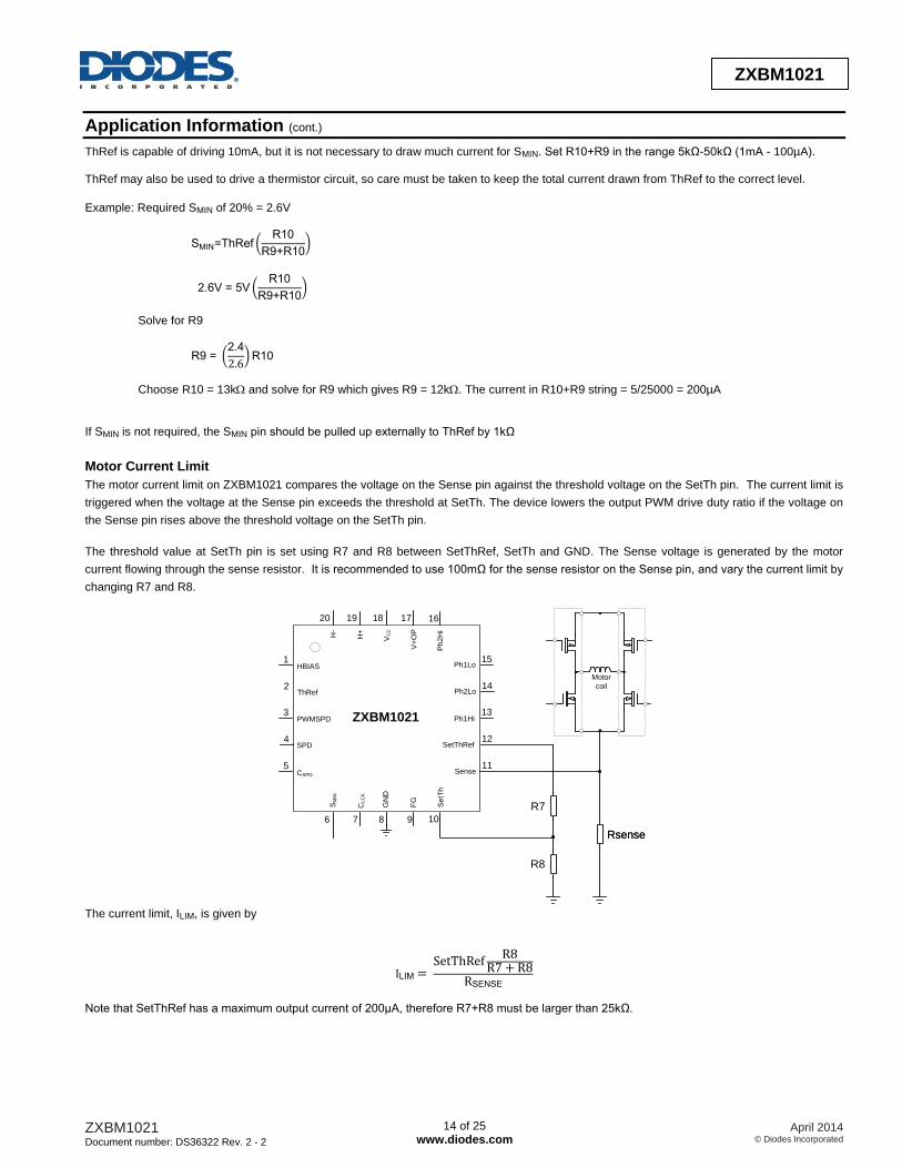
Motor Current Limit
The motor current limit on ZXBM1021 compares the voltage on the Sense pin against the threshold voltage on the SetTh pin. The current limit is
triggered when the voltage at the Sense pin exceeds the threshold at SetTh. The device lowers the output PWM drive duty ratio if the voltage on
the Sense pin rises above the threshold voltage on the SetTh pin.
The threshold value at SetTh pin is set using R7 and R8 between SetThRef, SetTh and GND. The Sense voltage is generated by the motor
current flowing through the sense resistor. It is recommended to use 100mΩ for the sense resistor on the ense pin, and vary the current limit by
changing R7 and R8.
The current limit, ILIM, is given by
IM
ote that etTh ef has a maximum output current of 200µA, therefore 7 8 must be larger than 25kΩ.
H+
ThRef
PWMSPD
Ph
2H
i
H-
SPD
FG
Ph1Lo
Ph2Lo
Ph1Hi
SetThRef
Sense
Se
tTh
GN
D
HBIAS
ZXBM1021
1
2
3
4
5
6 7 8 9 10
15
14
13
12
11
20 19 18 17 16
V+
OP
CL
CK
SM
IN
CSPD
VC
C
R7
R8
RsenseRsense
Motor
coil

ZXBM1021 Document number: DS36322 Rev. 2 - 2
15 of 25 www.diodes.com
April 2014 © Diodes Incorporated
ZXBM1021
Application Information (cont.)
Example: Required ILIM = 2A
IM
where SetThRef = (ThRef -0.1V) = 4.9V typical
Ω
Solve for R7
7 .9
8
Choose R8 = 2k and solve for R7 which gives R7 = 47k.
The current in R7+R8 string = 4.9/49000 = 100µA which is within maximum output current capability of the SetThRef pin.
It is important that the current limit be set above the intended average current of the motor. In practice, due to the variable nature of the motor
current through a commutation cycle, it is usually necessary for the current limit to be set higher than the peak current drawn at the beginning of
each commutation cycle.
The top trace shows the motor coil current, while the lower trace shows the Sense pin voltage. As the current flow direction in the motor coil
changes at each commutation cycle, the motor current in the top trace is shown as positive and negative current. The current flowing in the
Rsense is always in the same direction and therefore the sense pin reads the magnitude of the motor coil current.
Current limiting may prevent the motor from reaching full speed, despite the average current being significantly lower than the current limit. The
system will limit the tail-end current according to the current limit set. Current limit setting can also be used to remove the tail-end current.
Example of using current limit to reduce tail-end current at full speed is shown in fibelow
Current limit set much higher than the peak tail-end current
(Peak tail-end current = 180mA typ, Current limit set at 0.485mA )

ZXBM1021 Document number: DS36322 Rev. 2 - 2
16 of 25 www.diodes.com
April 2014 © Diodes Incorporated
ZXBM1021
Application Information (cont.)
Current limit set lower than the peak tail-end current
(Tail-end current = 145mA typ, Current limit set at 0.166mA)
CLCK Value
The value of CLCK affects three important timings for the ZXBM1021: Soft Start, Lock Detect and Off-time.
Soft Start
When the system is initially powered on, it will go through the soft-start period, during which the motor is gradually ramped to full speed. The soft
start operation relies on the current control feature being implemented and generally the current limit is set slightly above the normal running
current.
In the soft start process, at power-on the voltage at CLCK will rapidly increase to the low threshold, VCLCKTHL (0.6V). Then, CLCK will be charged
from 0.6V up to the high threshold, VCLCKTHH (5V) at a constant current, ILCKCL, which is typically 0.7µA. The the time taken to charge the
capacitor form VCLCKTHL to VCLCKTHH level depends on the value of CLCK capacitor. The soft-start time tss is given by:
Since VCLCKTHH, VCLCKTHL and ILCKCL are fixed, this becomes simply:
For the default value of CLCK, 0.47µF, soft-start time is:
This is the 3s stated in the datasheet electrical parameter section. Lock Detect
When the motor is running, the hall sensor will follow the rotor magnetic flux density to detect the commutation point. Should the rotor lock, the
signal from the hall sensor will cease. The value of CLCK defines the lock detect time period before the ZXBM1021 shuts down the outputs in
order to prevent damage to the coil.
The ZXBM1021 internal system returns CLCK voltage to the low threshold, VCLCKTHL (0.6V), each time the hall sensor provides a commutation
signal. CLCK then charges at the run current, ILCKCR, which is typically 5.5µA. If the voltage on CLCK reaches the high threshold, VCLCKTHH (5V),
before the hall sensor provides the next commutation signal then the system will shut down by entering the lock condition.
The thresholds voltage and charge current are fixed, therefore the time depends only on the value of CLCK:
For the default value of CLCK, 0.47µF, tLCKDET is as follows:
This should not interfere with normal operation of a fan as the time period for lock detection is many times longer than the expected time for one
revolution. As the hall sensor will detect 4 transitions in a single revolution, 0.376s between transitions would equate to a rotational speed of
40rpm. For use in systems where extremely low rotation speeds are required, the lock detect time can be increased by making the CLCK
capacitor value larger.
ZXBM1021 Document number: DS36322 Rev. 2 - 2
17 of 25 www.diodes.com
April 2014 © Diodes Incorporated
ZXBM1021
Application Information (cont.)
Off Time
If the above lock detection causes a device shutdown, CLCK is used again to provide the time period, tOFF. This is the time for which the device
will remain shut down after rotor lock is detected. The output shutdown period, tOFF, depends CLCK being discharged from the high threshold to
the low threshold at the discharge current ILCKDL, typically 0.7µA.
As above, the threshold voltages and discharge current are fixed, therefore the time depends only on the value of CLCK:
For the default value of CLCK, 0.47µF, tOFF is as follows:
FF
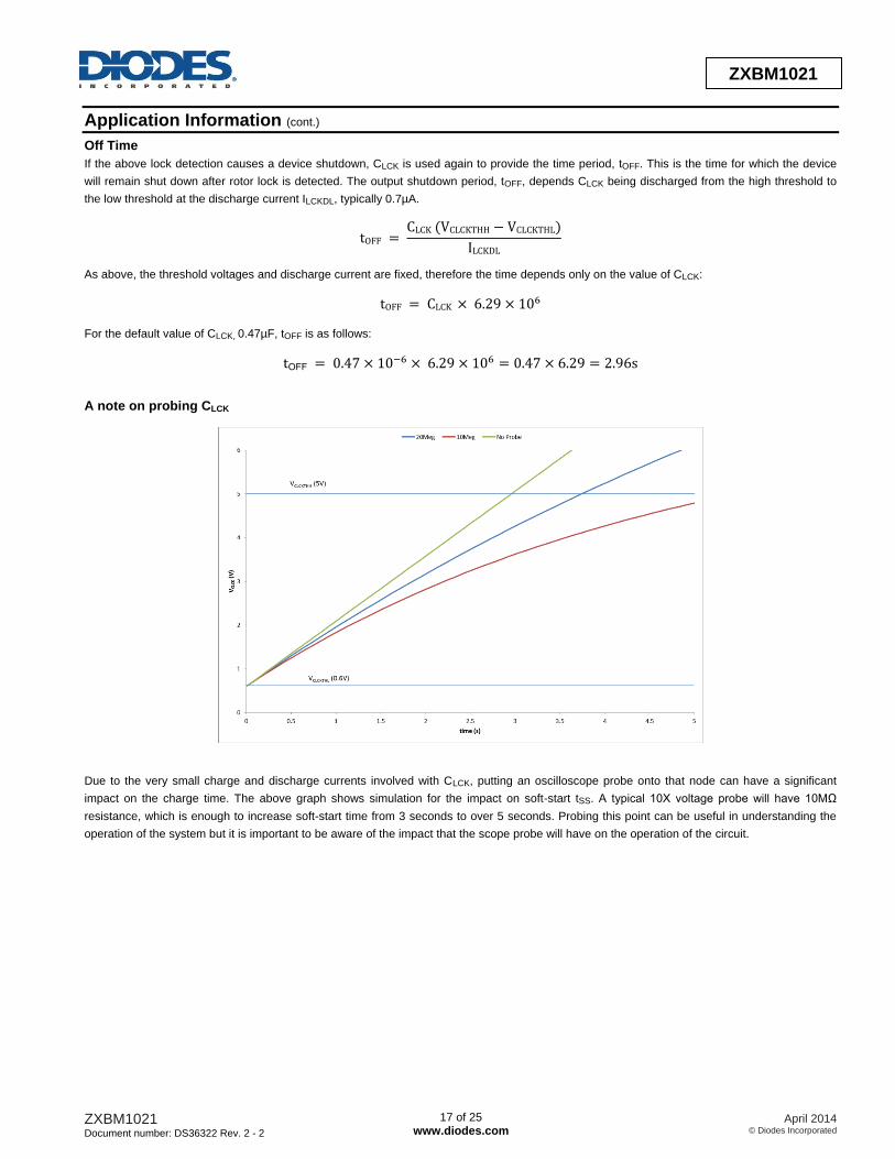
A note on probing CLCK
Due to the very small charge and discharge currents involved with CLCK, putting an oscilloscope probe onto that node can have a significant
impact on the charge time. The above graph shows simulation for the impact on soft-start tSS. A typical 10X voltage probe will have 10MΩ
resistance, which is enough to increase soft-start time from 3 seconds to over 5 seconds. Probing this point can be useful in understanding the
operation of the system but it is important to be aware of the impact that the scope probe will have on the operation of the circuit.

ZXBM1021 Document number: DS36322 Rev. 2 - 2
18 of 25 www.diodes.com
April 2014 © Diodes Incorporated
ZXBM1021
Application Information (cont.)
Output Device Driving
In order to drive the output stage efficiently, it is important to minimise shoot-through currents. The ZXBM1021 has a built-in delay (commutation
dead-time) to allow time for re-circulating currents to be absorbed however parasitic shoot-through can still occur. This is when the rapid switch-
on of the low-side MOSFET causes a low-going pulse through the high-side MOSFET to the gate, causing it to switch on momentarily. Slowing
the switch-on of the low-side MOSFET can eliminate this effect.
The resistors R1 to R6 and R12 in the diagram allow for control of switch-on and switch-off times for the top and bottom MOSFETs separately.
High-side MOSFETs switching speed:
R3 and R5 control the discharge of the gates of the high-side P-channel MOSFETSs, limiting the switch-on speed.
R4 and R6 control the charging of the gates of the P-channel MOSFETs, limiting the switch-off speed.
Low-side MOSFETs switching speed:
R1 and R2 are series gate resistors for the N-channel FETs, affecting both switch-on and switch-off times.
R12 is the series resistor for the V+OP pin of the ZXBM1021. This resistor is effectively in series with R1 or R2 when that
low-side N-channel device is switched on, limiting the switch-on time. R12 allows to vary the switch-on time relative to the
switch-off time to prevent parasitic shoot-through at turn-on. When using bipolar output devices the resistors serve similar functions in limiting the base currents of the transistors.
H+
ThRef
PWMSPD
Ph
2H
i
H-
SPD
FG
Ph1Lo
Ph2Lo
Ph1Hi
SetThRef
Sense
Se
tTh
GN
D
HBIAS
ZXBM1021
1
2
3
4
5
6 7 8 9 10
15
14
13
12
11
20 19 18 17 16
V+
OP
CL
CK
SM
IN
CSPD
VC
C
Rsense
Motor
coil
R5 R3
R6 R4
R1 R2
R12
D2
D1D1
Optional,
system dependent
Op
tio
na
l
System supply
(12V)
ZXBM1021 Document number: DS36322 Rev. 2 - 2
19 of 25 www.diodes.com
April 2014 © Diodes Incorporated
ZXBM1021
Application Information (cont.)
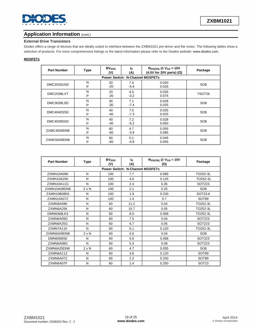
External Drive Transistors
Diodes offers a range of devices that are ideally suited to interface between the ZXBM1021 pre-driver and the motor. The following tables show a
selection of products. For more comprehensive listings or the latest information please refer to the Diodes website: www.diodes.com. MOSFETs
Part Number Type BVDSS
(V)
ID
(A)
RDS(ON) @ VGS = 10V
(4.5V for 20V parts) (Ω) Package
Power Switch: N-Channel MOSFETs
DMC2020USD N
P
20 -20
7.4 -5.9
0.020 0.033
SO8
DMC2038LVT N
P
20 -20
4.5 -3.2
0.035 0.074
TSOT26
DMC3028LSD N
P
30 -30
7.1 -7.4
0.028 0.025
SO8
DMC4040SSD N
P
40 -40
7.5 -7.3
0.025 0.025
SO8
DMC4028SSD N
P
40 -40
7.2 -5.2
0.028 0.050
SO8
ZXMC4559DN8 N
P
60 -60
4.7 -3.9
0.055 0.085
SO8
ZXMC6A09DN8 N
P
60 -60
5.1 -4.8
0.045 0.055
SO8
Part Number Type BVDSS
(V)
ID
(A)
RDS(ON) @ VGS = 10V
(Ω) Package
Power Switch: N-Channel MOSFETs
ZXMN10A09K N 100 7.7 0.085 TO252-3L
ZXMN10A25K N 100 4.0 0.125 TO252-3L
ZXMN10A11G N 100 2.4 0.35 SOT223
ZXMN10A08DN8 2 x N 100 2.1 0.25 SO8
ZXMN10B08E6 N 100 1.9 0.230 SOT23-6
ZXMN10A07Z N 100 1.4 0.7 SOT89
ZXMN6A09K N 60 11.2 0.04 TO252-3L
ZXMN6A25K N 60 10.7 0.05 TO252-3L
DMN6068LK3 N 60 8.5 0.068 TO252-3L
ZXMN6A09G N 60 7.5 0.04 SOT223
ZXMN6A25G N 60 6.7 0.05 SOT223
ZXMN7A11K N 60 6.1 0.120 TO252-3L
ZXMN6A09DN8 2 x N 60 5.6 0.04 SO8
DMN6068SE N 60 5.6 0.068 SOT223
ZXMN6A08G N 60 5.3 0.08 SOT223
ZXMN6A25DN8 2 x N 60 4.7 0.055 SO8
ZXMN6A11Z N 60 3.6 0.120 SOT89
ZXMN6A07Z N 60 2.2 0.250 SOT89
ZXMN6A07F N 60 1.4 0.250 SOT23
ZXBM1021 Document number: DS36322 Rev. 2 - 2
20 of 25 www.diodes.com
April 2014 © Diodes Incorporated
ZXBM1021
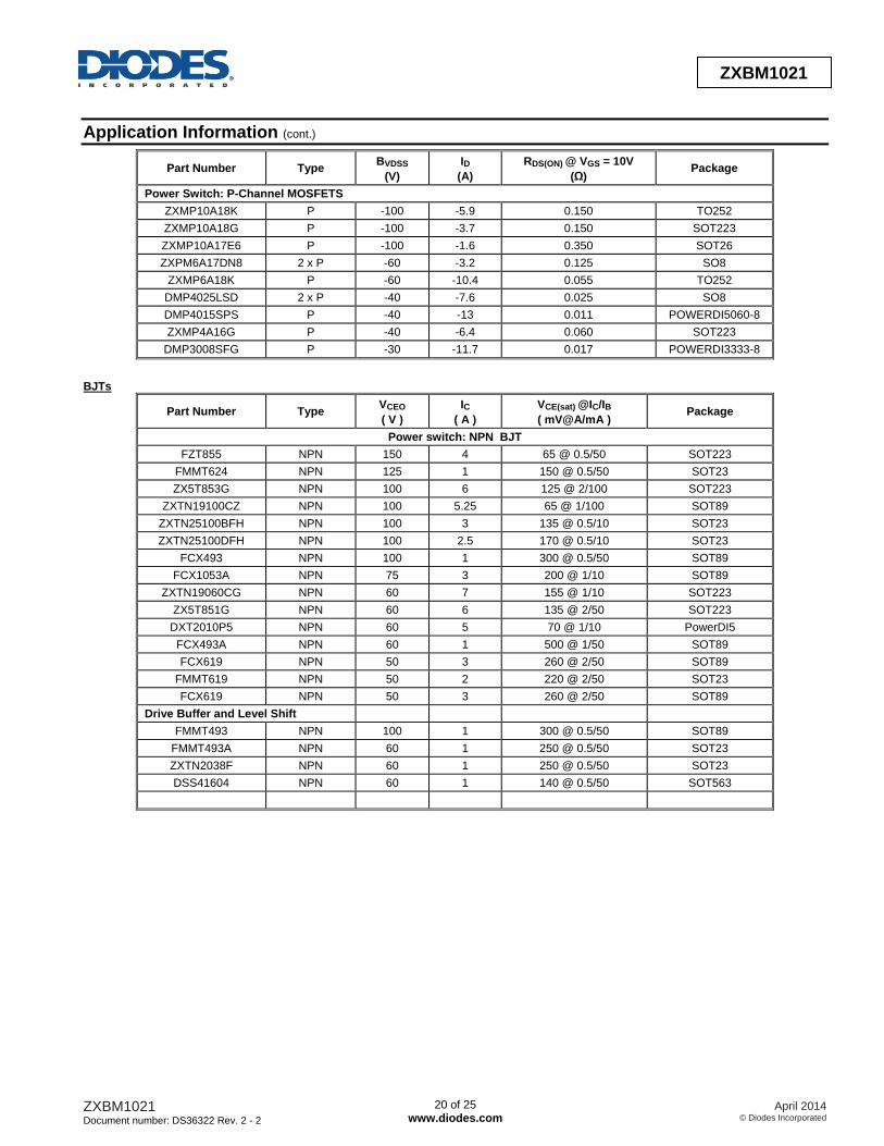
Application Information (cont.)
Part Number Type BVDSS
(V)
ID
(A)
RDS(ON) @ VGS = 10V
(Ω) Package
Power Switch: P-Channel MOSFETS
ZXMP10A18K P -100 -5.9 0.150 TO252
ZXMP10A18G P -100 -3.7 0.150 SOT223
ZXMP10A17E6 P -100 -1.6 0.350 SOT26
ZXPM6A17DN8 2 x P -60 -3.2 0.125 SO8
ZXMP6A18K P -60 -10.4 0.055 TO252
DMP4025LSD 2 x P -40 -7.6 0.025 SO8
DMP4015SPS P -40 -13 0.011 POWERDI5060-8
ZXMP4A16G P -40 -6.4 0.060 SOT223
DMP3008SFG P -30 -11.7 0.017 POWERDI3333-8
BJTs
Part Number Type VCEO
( V )
IC
( A )
VCE(sat) @IC/IB
( mV@A/mA ) Package
Power switch: NPN BJT
FZT855 NPN 150 4 65 @ 0.5/50 SOT223
FMMT624 NPN 125 1 150 @ 0.5/50 SOT23
ZX5T853G NPN 100 6 125 @ 2/100 SOT223
ZXTN19100CZ NPN 100 5.25 65 @ 1/100 SOT89
ZXTN25100BFH NPN 100 3 135 @ 0.5/10 SOT23
ZXTN25100DFH NPN 100 2.5 170 @ 0.5/10 SOT23
FCX493 NPN 100 1 300 @ 0.5/50 SOT89
FCX1053A NPN 75 3 200 @ 1/10 SOT89
ZXTN19060CG NPN 60 7 155 @ 1/10 SOT223
ZX5T851G NPN 60 6 135 @ 2/50 SOT223
DXT2010P5 NPN 60 5 70 @ 1/10 PowerDI5
FCX493A NPN 60 1 500 @ 1/50 SOT89
FCX619 NPN 50 3 260 @ 2/50 SOT89
FMMT619 NPN 50 2 220 @ 2/50 SOT23
FCX619 NPN 50 3 260 @ 2/50 SOT89
Drive Buffer and Level Shift
FMMT493 NPN 100 1 300 @ 0.5/50 SOT89
FMMT493A NPN 60 1 250 @ 0.5/50 SOT23
ZXTN2038F NPN 60 1 250 @ 0.5/50 SOT23
DSS41604 NPN 60 1 140 @ 0.5/50 SOT563
ZXBM1021 Document number: DS36322 Rev. 2 - 2
21 of 25 www.diodes.com
April 2014 © Diodes Incorporated
ZXBM1021
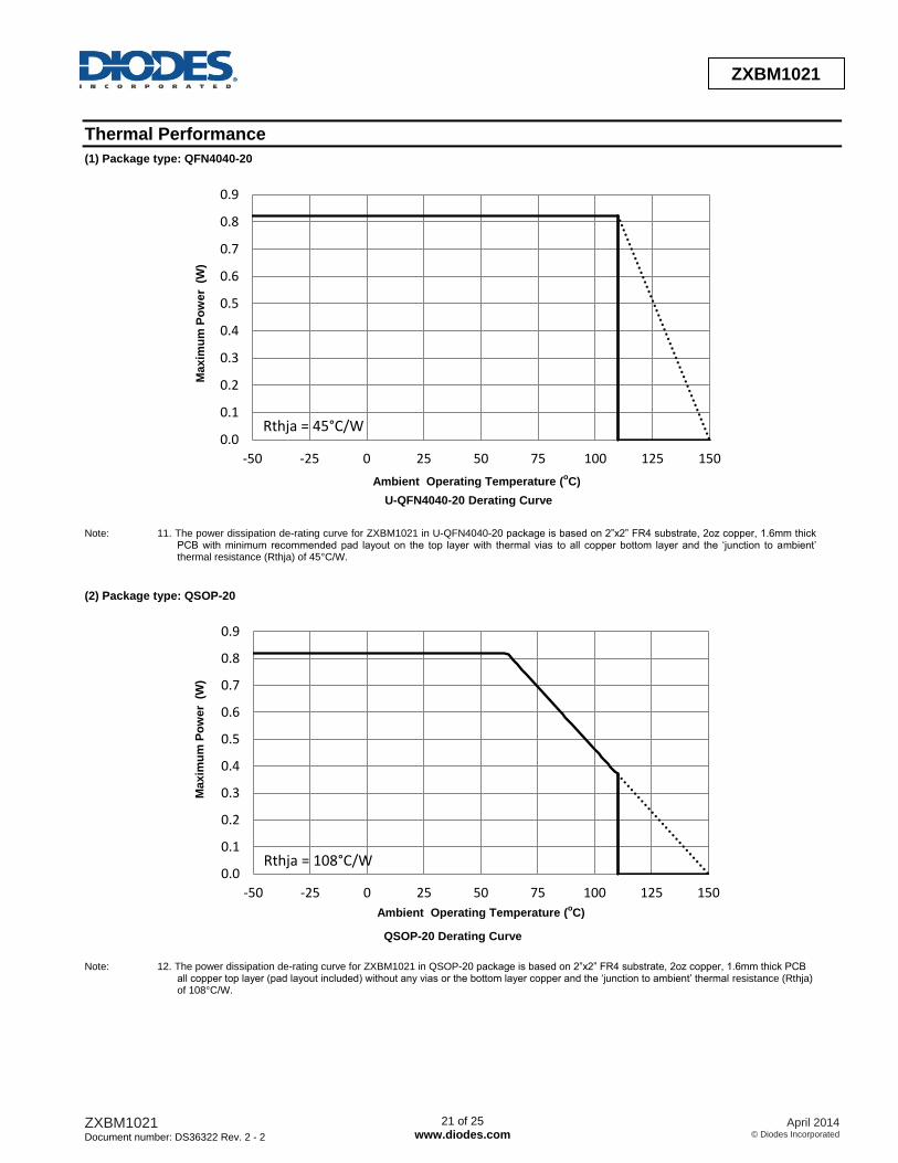
Thermal Performance
(1) Package type: QFN4040-20
Note: 11. The power dissipation de-rating curve for ZXBM1021 in U-QFN4040-20 package is based on 2”x2” F substrate, 2oz copper, 1. mm thick
PCB with minimum recommended pad layout on the top layer with thermal vias to all copper bottom layer and the ‘junction to ambient’ thermal resistance (Rthja) of 45°C/W.
(2) Package type: QSOP-20
Note: 12. The power dissipation de-rating curve for ZXBM1021 in QSOP-20 package is based on 2”x2” F substrate, 2oz copper, 1. mm thick PCB
all copper top layer (pad layout included) without any vias or the bottom layer copper and the ‘junction to ambient’ thermal resistance (Rthja) of 108°C/W.
0.0
0.1
0.2
0.3
0.4
0.5
0.6
0.7
0.8
0.9
-50 -25 0 25 50 75 100 125 150
Maxim
um
Po
wer
(W
)
Ambient Operating Temperature (oC)
U-QFN4040-20 Derating Curve
Rthja = 45°C/W
0.0
0.1
0.2
0.3
0.4
0.5
0.6
0.7
0.8
0.9
-50 -25 0 25 50 75 100 125 150
Maxim
um
Po
wer
(W
)
Ambient Operating Temperature (oC)
QSOP-20 Derating Curve
Rthja = 108°C/W

ZXBM1021 Document number: DS36322 Rev. 2 - 2
22 of 25 www.diodes.com
April 2014 © Diodes Incorporated
ZXBM1021
Ordering Information
ZXBM1021 - XXX - XX
PackingPackage
TC : Tape & Reel JB20 : U-QFN4040-20
Q20 : QSOP-20
Part Number Package Code Packaging 13” Tape and Reel
Quantity Part Number Suffix
ZXBM1021JB20TC JB20 U-QFN4040-20 3000/Tape & Reel TC
ZXBM1021Q20TC Q20 QSOP-20 2500/Tape & Reel TC
Marking Information
(1) Package type: U-QFN4040-20
( Top View )
1021
YY : Year : 00 ~ 99; WW : Week: 01 ~ 52 week;
52 Represents 52 and 53 weekYY WW
ZXBM
Part Number Package Identification Code
ZXBM1021JB20TC QFN4040-20 ZXBM 1021
(2) Package type: QSOP-20
WW : Week: 01 ~ 52 week;
(Top View)
YY : Year: 00 ~ 99;
52 represents 52 and 53 week
1
YY WW
20
ZXBM1021
Part Number Package Identification Code
ZXBM1021Q20TC QSOP-20 ZXBM1021

ZXBM1021 Document number: DS36322 Rev. 2 - 2
23 of 25 www.diodes.com
April 2014 © Diodes Incorporated
ZXBM1021
Package Outline Dimensions (All dimensions in mm.)
Please see AP02002 at http://www.diodes.com/datasheets/ap02002.pdf for latest version.
(1) Package type: U-QFN4040-20
(2) Package Type: QSOP-20
U-QFN4040-20
Dim Min Max Typ
A 0.55 0.65 0.60
A1 0 0.05 0.02
A3 - - 0.15
b 0.20 0.30 0.25
D 3.95 4.05 4.00
D2 2.40 2.60 2.50
E 3.95 4.05 4.00
E2 2.40 2.60 2.50
e 0.50 BSC
L 0.35 0.45 0.40
Z - - 0.875
All Dimensions in mm
QSOP-20
Dim Min Max Typ
A 1.55 1.73 -
A1 0.10 0.25 -
A2 1.40 1.50 -
b 0.20 0.30 -
c 0.18 0.25 -
D 8.56 8.74 -
E 5.79 6.20 -
E1 3.81 3.99 -
e 0.635 BSC
h 0.254 0.508 -
L 0.41 1.27 -
L1 1.03 REF
L2 0.254 BSC
R 0.0762 - -
R1 0.0762 - -
ZD 1.47 REF
θ 0° 8° -
θ1 5° 15° -
θ2 0° - -
All Dimensions in mm
D
D2
E
b
L
E2
A
A1A3
(Pin #1 ID)
Seating Plane
Z (8x)
e
D
E1 E
ZD
E/2
E1/2
e
b 20x
PIN 1
A2A
A1
SEE DETAIL 'A'
L
L1
GAUGE PLANE
SEATING PLANE
L2
1
1
h
h
R1
R
2
c

ZXBM1021 Document number: DS36322 Rev. 2 - 2
24 of 25 www.diodes.com
April 2014 © Diodes Incorporated
ZXBM1021
Suggested Pad Layout
Please see AP02001 at http://www.diodes.com/datasheets/ap02001.pdf for the latest version. (1) Package Type: U-QFN4040-20 (2) Package Type: QSOP-20
Dimensions Value
(in mm)
C 0.500
X 0.350
X1 0.600
X2 2.500
X3 4.300
Y 0.600
Y1 0.350
Y2 2.500
Y3 4.300
Dimensions Value
(in mm)
C 0.635
X 0.350
X1 6.065
Y 1.450
Y1 6.400
1
Y3
X3
Y1(10x)
X1(10x)
Y2
X2
X(10x) C
Y(10x)
1
Y1
X1
Y 20x
C
X 20x

ZXBM1021 Document number: DS36322 Rev. 2 - 2
25 of 25 www.diodes.com
April 2014 © Diodes Incorporated
ZXBM1021
IMPORTANT NOTICE DIODES INCORPORATED MAKES NO WARRANTY OF ANY KIND, EXPRESS OR IMPLIED, WITH REGARDS TO THIS DOCUMENT, INCLUDING, BUT NOT LIMITED TO, THE IMPLIED WARRANTIES OF MERCHANTABILITY AND FITNESS FOR A PARTICULAR PURPOSE (AND THEIR EQUIVALENTS UNDER THE LAWS OF ANY JURISDICTION). Diodes Incorporated and its subsidiaries reserve the right to make modifications, enhancements, improvements, corrections or other changes without further notice to this document and any product described herein. Diodes Incorporated does not assume any liability arising out of the application or use of this document or any product described herein; neither does Diodes Incorporated convey any license under its patent or trademark rights, nor the rights of others. Any Customer or user of this document or products described herein in such applications shall assume all risks of such use and will agree to hold Diodes Incorporated and all the companies whose products are represented on Diodes Incorporated website, harmless against all damages. Diodes Incorporated does not warrant or accept any liability whatsoever in respect of any products purchased through unauthorized sales channel. Should Customers purchase or use Diodes Incorporated products for any unintended or unauthorized application, Customers shall indemnify and hold Diodes Incorporated and its representatives harmless against all claims, damages, expenses, and attorney fees arising out of, directly or indirectly, any claim of personal injury or death associated with such unintended or unauthorized application. Products described herein may be covered by one or more United States, international or foreign patents pending. Product names and markings noted herein may also be covered by one or more United States, international or foreign trademarks. This document is written in English but may be translated into multiple languages for reference. Only the English version of this document is the final and determinative format released by Diodes Incorporated.
LIFE SUPPORT Diodes Incorporated products are specifically not authorized for use as critical components in life support devices or systems without the express written approval of the Chief Executive Officer of Diodes Incorporated. As used herein: A. Life support devices or systems are devices or systems which: 1. are intended to implant into the body, or
2. support or sustain life and whose failure to perform when properly used in accordance with instructions for use provided in the labeling can be reasonably expected to result in significant injury to the user.
B. A critical component is any component in a life support device or system whose failure to perform can be reasonably expected to cause the failure of the life support device or to affect its safety or effectiveness. Customers represent that they have all necessary expertise in the safety and regulatory ramifications of their life support devices or systems, and acknowledge and agree that they are solely responsible for all legal, regulatory and safety-related requirements concerning their products and any use of Diodes Incorporated products in such safety-critical, life support devices or systems, notwithstanding any devices- or systems-related information or support that may be provided by Diodes Incorporated. Further, Customers must fully indemnify Diodes Incorporated and its representatives against any damages arising out of the use of Diodes Incorporated products in such safety-critical, life support devices or systems. Copyright © 2014, Diodes Incorporated www.diodes.com