1
CMOSDigital Integrated
CircuitsAnalysis and Design
Chapter 8
Sequential MOS LogicCircuits
2
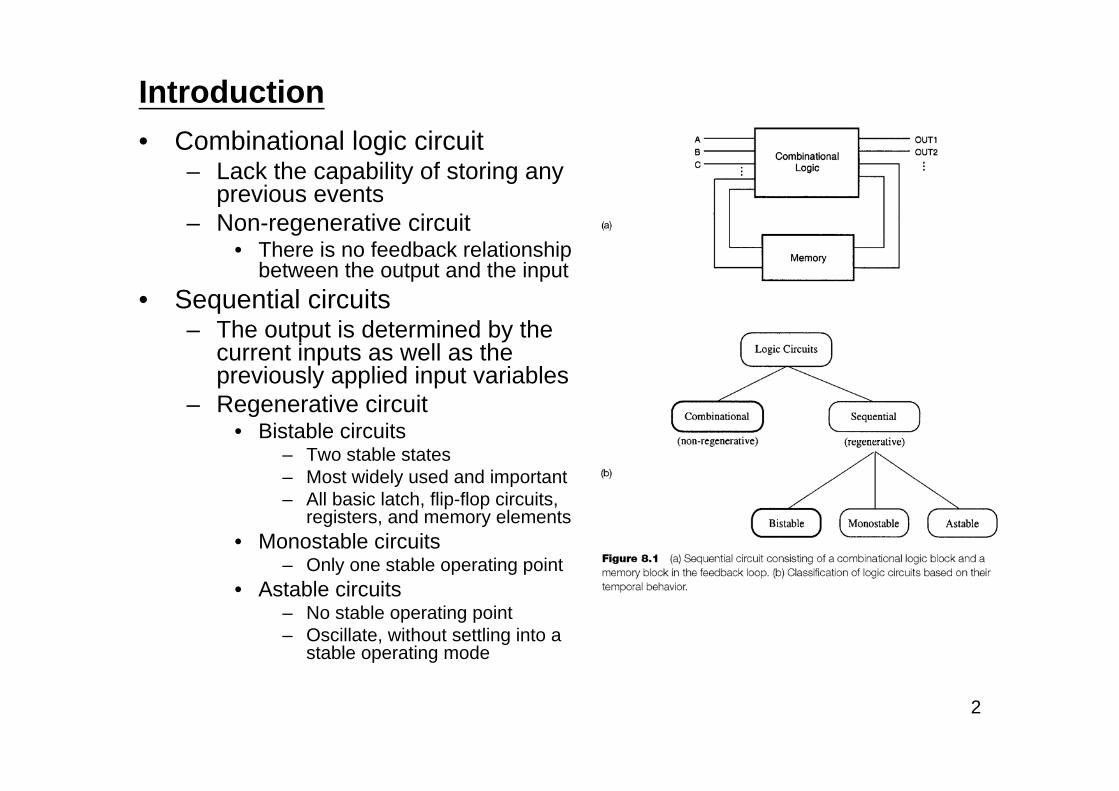
Introduction • Combinational logic circuit
– Lack the capability of storing any previous events
– Non-regenerative circuit• There is no feedback relationship
between the output and the input• Sequential circuits
– The output is determined by the current inputs as well as the previously applied input variables
– Regenerative circuit• Bistable circuits
– Two stable states– Most widely used and important– All basic latch, flip-flop circuits,
registers, and memory elements• Monostable circuits
– Only one stable operating point• Astable circuits
– No stable operating point– Oscillate, without settling into a
stable operating mode
3
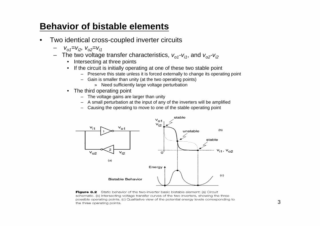
Behavior of bistable elements• Two identical cross-coupled inverter circuits
– vo1=vi2, vo2=vi1– The two voltage transfer characteristics, vo1-vi1, and vo2-vi2
• Intersecting at three points • If the circuit is initially operating at one of these two stable point
– Preserve this state unless it is forced externally to change its operating point– Gain is smaller than unity (at the two operating points)
» Need sufficiently large voltage perturbation• The third operating point
– The voltage gains are larger than unity– A small perturbation at the input of any of the inverters will be amplified– Causing the operating to move to one of the stable operating point
4
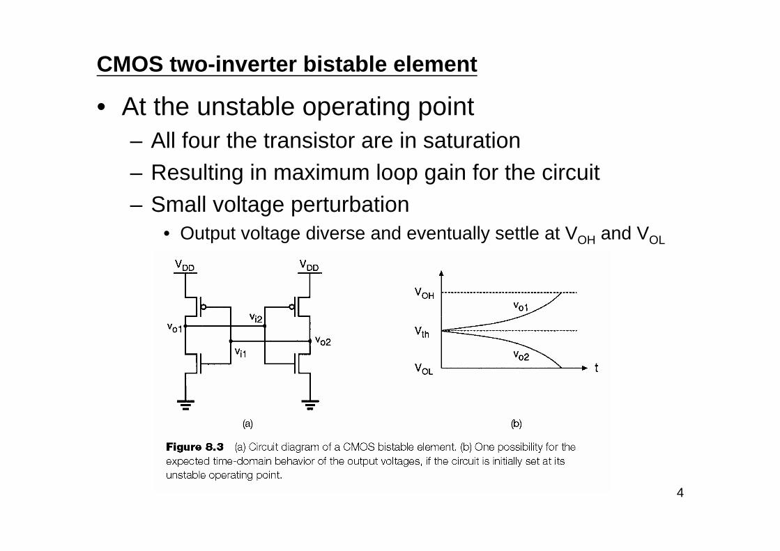
CMOS two-inverter bistable element
• At the unstable operating point– All four the transistor are in saturation– Resulting in maximum loop gain for the circuit– Small voltage perturbation
• Output voltage diverse and eventually settle at VOH and VOL
5
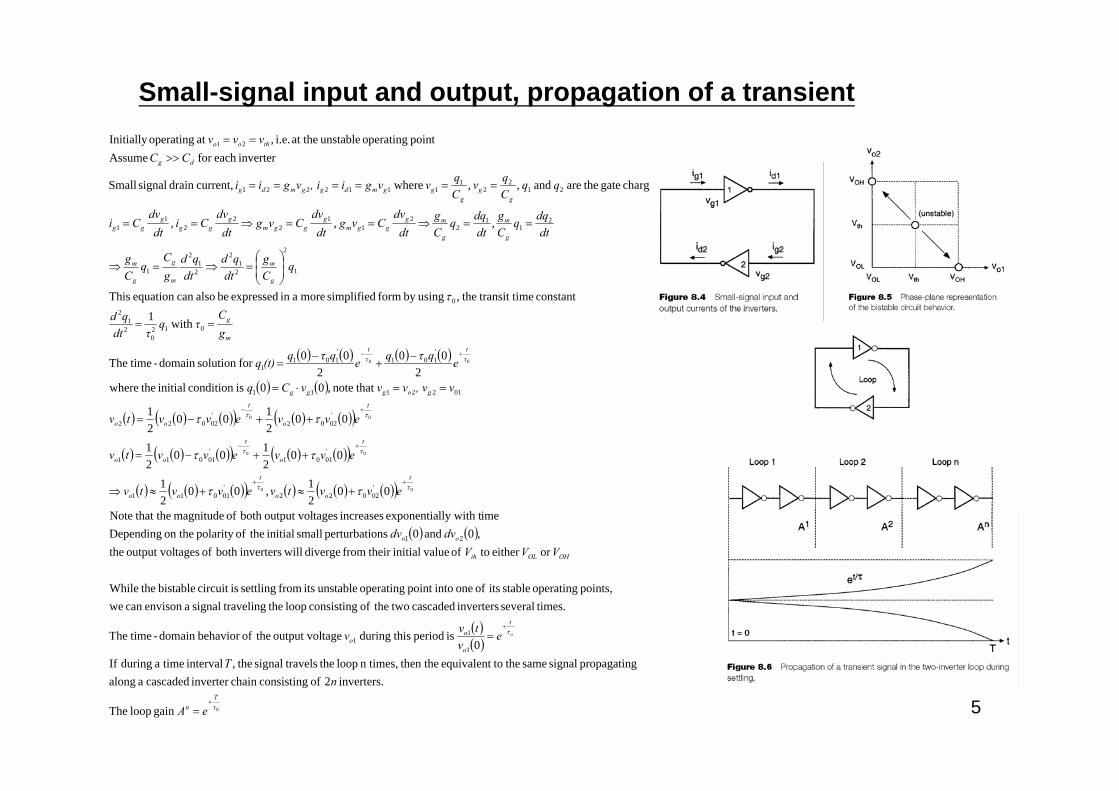
Small-signal input and output, propagation of a transient
( ) ( ) ( ) ( )
( ) ( )
( ) ( ) ( )( ) ( ) ( )( )
( ) ( ) ( )( ) ( ) ( )( )
( ) ( ) ( )( ) ( ) ( ) ( )( )
( ) ( )
( )( )
0
00
00
00
00
gain loop The
inverters. 2 of consistingchain inverter cascaded a alonggpropagatin signal same the toequivalent then then times, loop the travelssignal the, interval timea during If
0 is period thisduring tageoutput vol theofbehavior domain - timeThe
times.several inverters cascaded two theof consisting loop the travelingsignal aenvison can wepoints, operating stable its of one intopoint operating unstable its from settling iscircuit bistable theWhile
or either to of valueinitial their from diverge willinvertersboth of tagesoutput vol the ,0 and 0 onsperturbati small initial theofpolarity on the Dependingimelly with texponentia increases tagesoutput volboth of magnitude that theNote
0021,00
21
002100
21
002100
21
that note ,00iscondition initial thewhere2
002
00for solution domain - timeThe
with 1
constant ime transit t the, usingby form simplified more ain expressed be alsocan equation This
, , ,
charge gate theare and , , where current,drain signal Small
invertereach for Assumepoint operating unstable at the i.e. ,at operatingInitially
1
11
21
'02022
'01011
'0101
'01011
'0202
'02022
0122111
1011011
0120
21
20
1
2
21
2
21
2
1
21
12
21
12
22
11
212
21
1112221
21
τT
n
t
o
oo
OHOLth
oo
t
oo
t
oo
t
o
t
oo
t
o
t
oo
goggg
τt'
τt'
m
g
g
m
m
g
g
m
g
m
g
mgggm
gggm
ggg
ggg
gg
gggmdggmdg
dg
thoo
eA
nT
ev
tv v
VVVdvdv
evvtvevvtv
evvevvtv
evvevvtv
v, vvvvC q
eqτqeqτq(t)q
gC
τqτdt
qd
qCg
dtqd
dtqd
gC
qCg
dtdqq
Cg
dtdqq
Cg
dtdv
Cvgdt
dvCvg
dtdv
Cidt
dvCi
qqCqv
Cqvvgi, ivgii
CCvvv
o
+
+
++
+−
+−
+−
=
=
+≈+≈⇒
++−=
++−=
==⋅=
−+
−=
==
⎟⎟⎠
⎞⎜⎜⎝
⎛=⇒=⇒
==⇒==⇒==
======
>>==
τ
ττ
ττ
ττ
ττ
ττ
ττ
τ
6
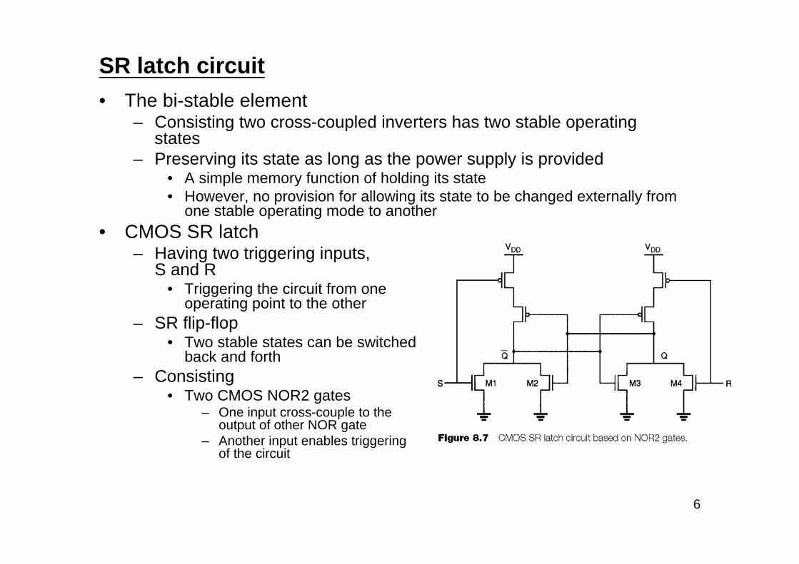
SR latch circuit• The bi-stable element
– Consisting two cross-coupled inverters has two stable operating states
– Preserving its state as long as the power supply is provided• A simple memory function of holding its state• However, no provision for allowing its state to be changed externally from
one stable operating mode to another• CMOS SR latch
– Having two triggering inputs, S and R
• Triggering the circuit from one operating point to the other
– SR flip-flop• Two stable states can be switched
back and forth– Consisting
• Two CMOS NOR2 gates– One input cross-couple to the
output of other NOR gate– Another input enables triggering
of the circuit
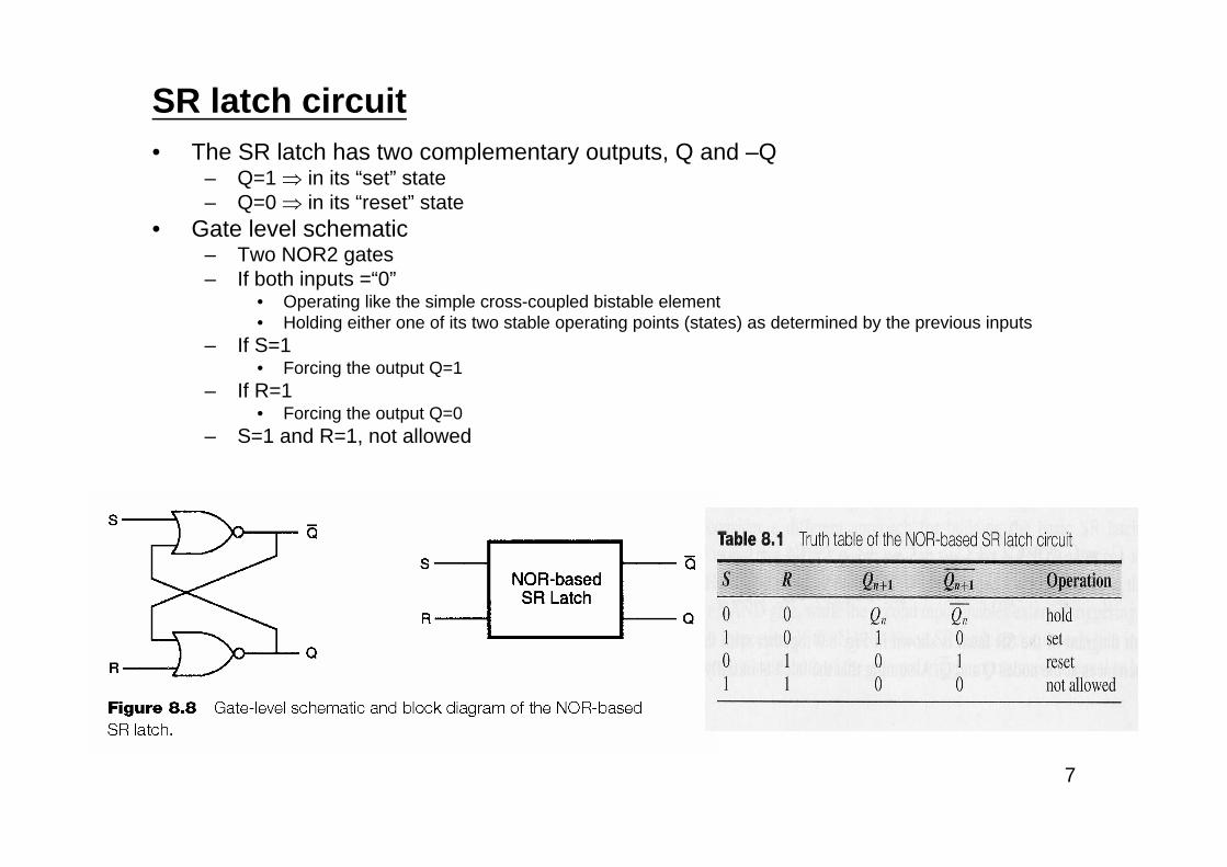
7
SR latch circuit• The SR latch has two complementary outputs, Q and –Q
– Q=1 ⇒ in its “set” state– Q=0 ⇒ in its “reset” state
• Gate level schematic– Two NOR2 gates– If both inputs =“0”
• Operating like the simple cross-coupled bistable element• Holding either one of its two stable operating points (states) as determined by the previous inputs
– If S=1• Forcing the output Q=1
– If R=1• Forcing the output Q=0
– S=1 and R=1, not allowed
8
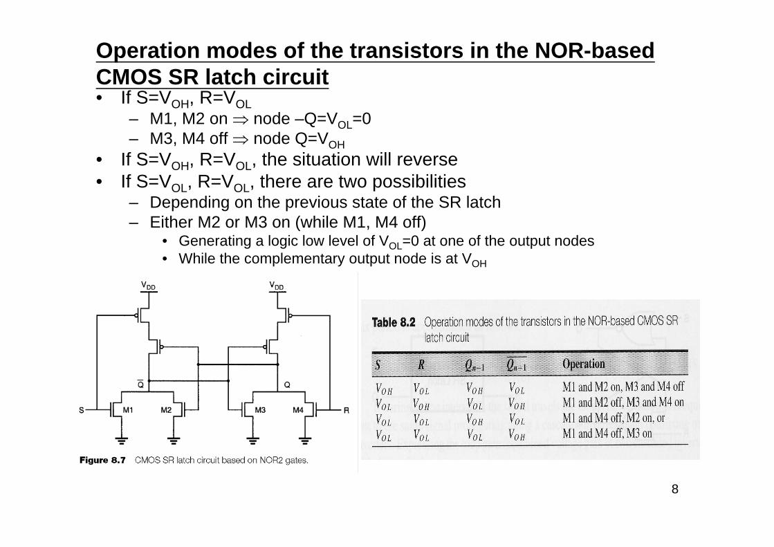
Operation modes of the transistors in the NOR-based CMOS SR latch circuit• If S=VOH, R=VOL
– M1, M2 on ⇒ node –Q=VOL=0– M3, M4 off ⇒ node Q=VOH
• If S=VOH, R=VOL, the situation will reverse• If S=VOL, R=VOL, there are two possibilities
– Depending on the previous state of the SR latch– Either M2 or M3 on (while M1, M4 off)
• Generating a logic low level of VOL=0 at one of the output nodes• While the complementary output node is at VOH
9
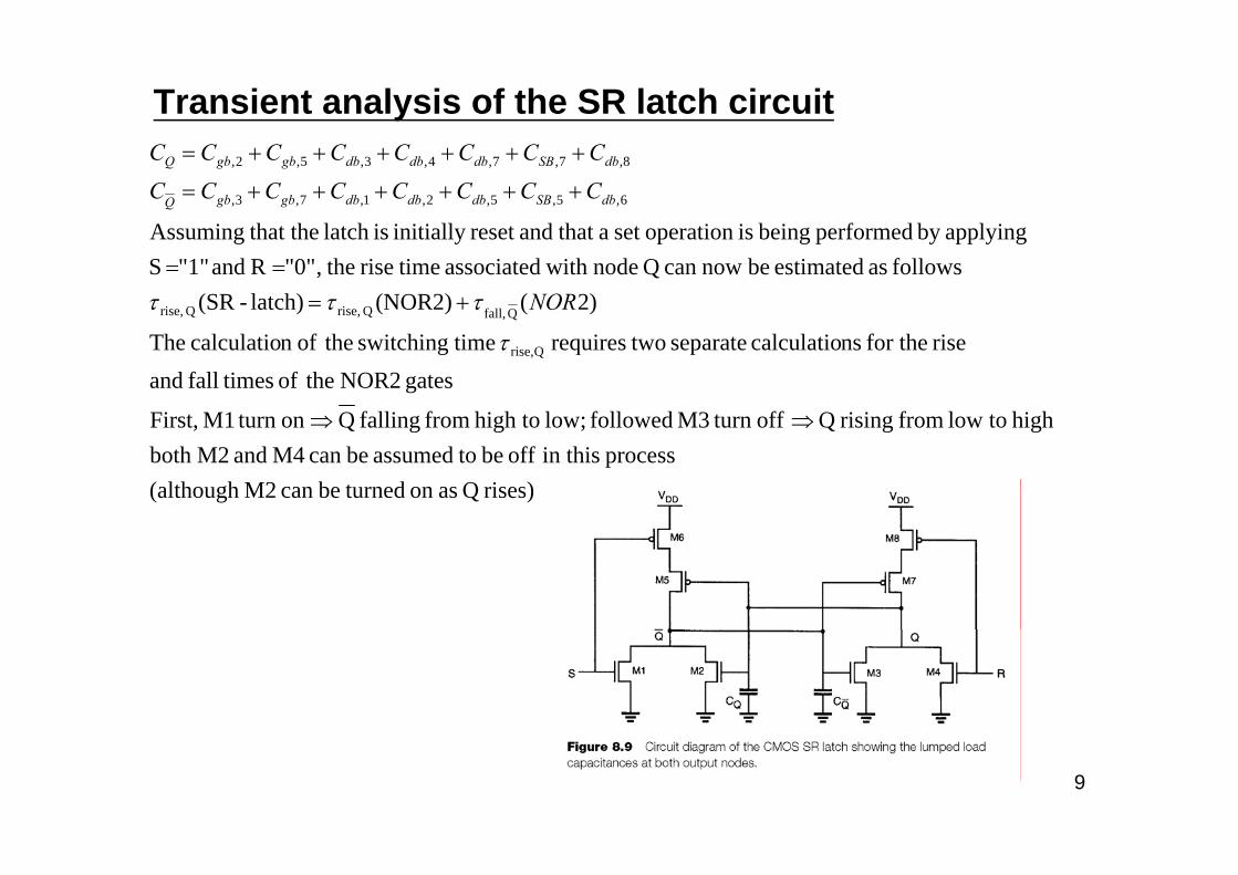
Transient analysis of the SR latch circuit
rises) Q ason turnedbecan M2(although process in this off be toassumed becan M4 and M2both
high tolow from rising Q off turn M3 followed low; high to from falling Qon turn M1 First,
gates NOR2 theof timesfall and rise for the nscalculatio separate tworequires timeswitching theofn calculatio The
)2( (NOR2)latch)-(SRfollows as estimated be nowcan Q node with associated timerise the,"0"R and "1"S
applyingby performed being isoperation set a that andreset initially islatch that theAssuming
Qrise,
Q fall,Q rise,Q rise,
6,5,5,2,1,7,3,
8,7,7,4,3,5,2,
⇒⇒
+===
++++++=
++++++=
τ
τττ NOR
CCCCCCCC
CCCCCCCC
dbSBdbdbdbgbgbQ
dbSBdbdbdbgbgbQ
10
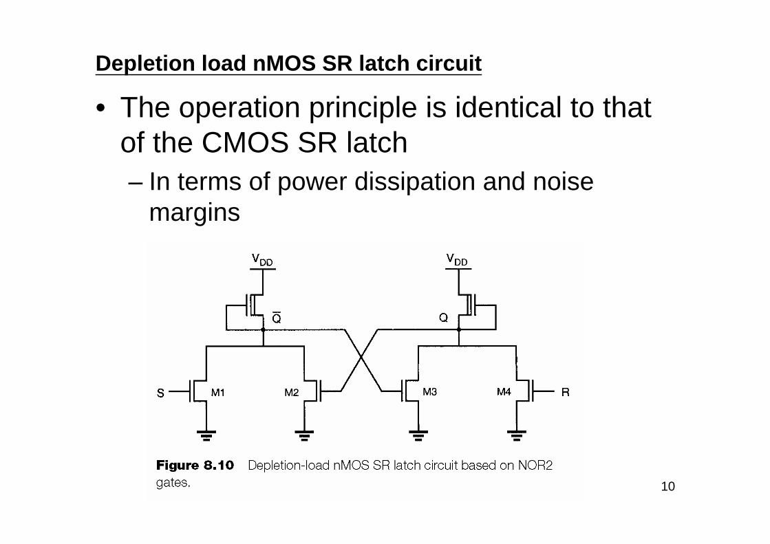
Depletion load nMOS SR latch circuit
• The operation principle is identical to that of the CMOS SR latch– In terms of power dissipation and noise
margins
11
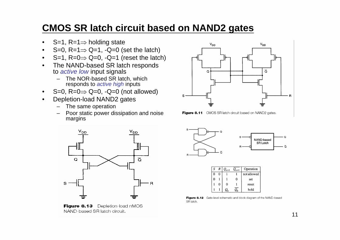
CMOS SR latch circuit based on NAND2 gates• S=1, R=1⇒ holding state• S=0, R=1⇒ Q=1, -Q=0 (set the latch)• S=1, R=0⇒ Q=0, -Q=1 (reset the latch)• The NAND-based SR latch responds
to active low input signals– The NOR-based SR latch, which
responds to active high inputs• S=0, R=0⇒ Q=0, -Q=0 (not allowed)• Depletion-load NAND2 gates
– The same operation– Poor static power dissipation and noise
margins
12
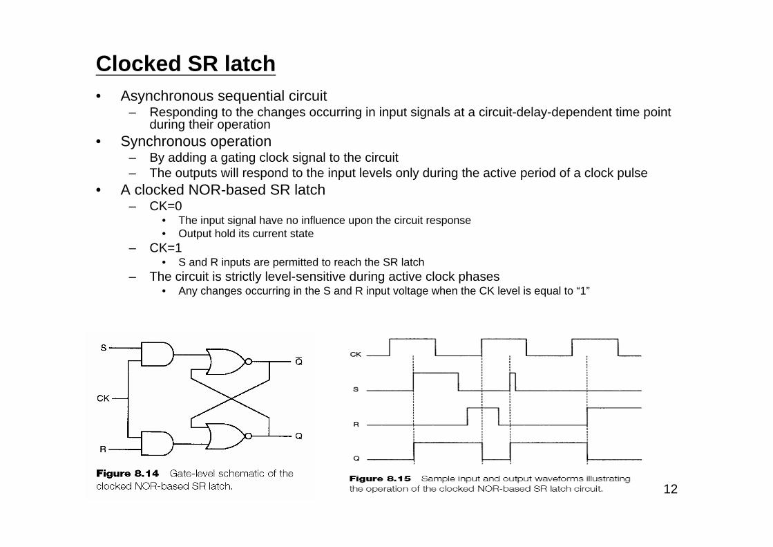
Clocked SR latch• Asynchronous sequential circuit
– Responding to the changes occurring in input signals at a circuit-delay-dependent time point during their operation
• Synchronous operation– By adding a gating clock signal to the circuit– The outputs will respond to the input levels only during the active period of a clock pulse
• A clocked NOR-based SR latch– CK=0
• The input signal have no influence upon the circuit response• Output hold its current state
– CK=1• S and R inputs are permitted to reach the SR latch
– The circuit is strictly level-sensitive during active clock phases• Any changes occurring in the S and R input voltage when the CK level is equal to “1”
13
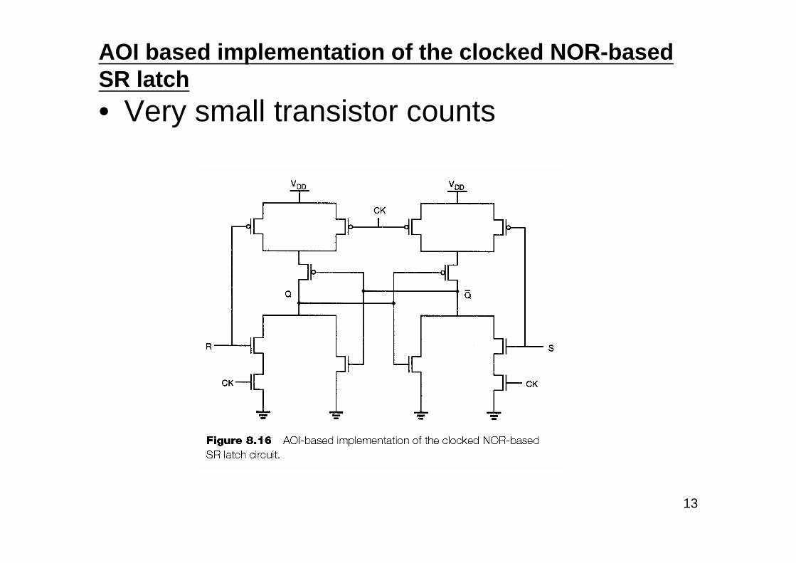
AOI based implementation of the clocked NOR-based SR latch• Very small transistor counts
14
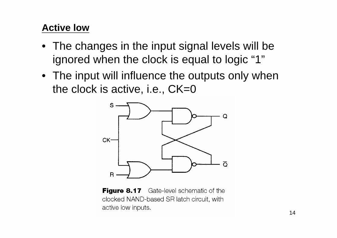
Active low
• The changes in the input signal levels will be ignored when the clock is equal to logic “1”
• The input will influence the outputs only when the clock is active, i.e., CK=0
15
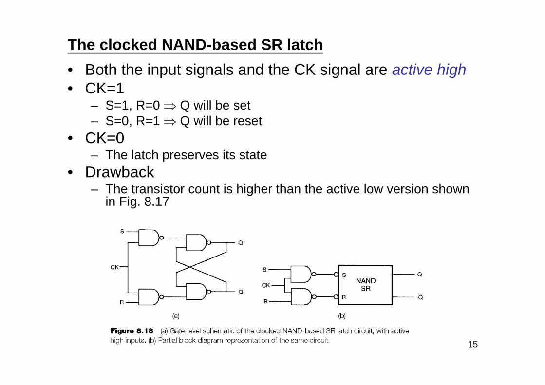
The clocked NAND-based SR latch• Both the input signals and the CK signal are active high• CK=1
– S=1, R=0 ⇒ Q will be set– S=0, R=1 ⇒ Q will be reset
• CK=0– The latch preserves its state
• Drawback– The transistor count is higher than the active low version shown
in Fig. 8.17
16
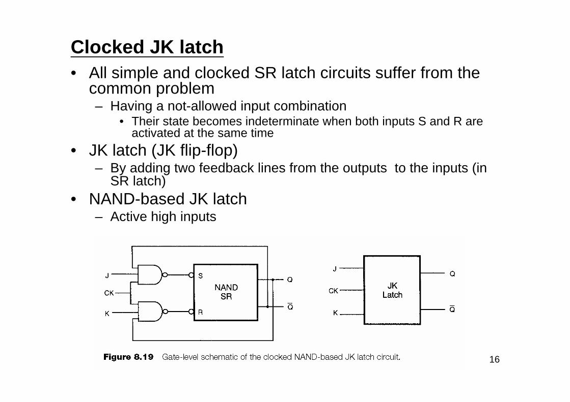
Clocked JK latch• All simple and clocked SR latch circuits suffer from the
common problem– Having a not-allowed input combination
• Their state becomes indeterminate when both inputs S and R are activated at the same time
• JK latch (JK flip-flop)– By adding two feedback lines from the outputs to the inputs (in
SR latch) • NAND-based JK latch
– Active high inputs
17
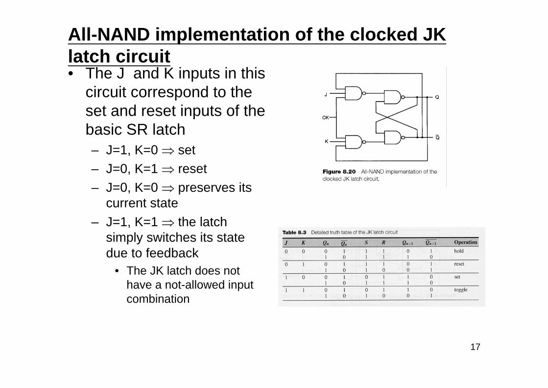
All-NAND implementation of the clocked JK latch circuit• The J and K inputs in this
circuit correspond to the set and reset inputs of the basic SR latch– J=1, K=0 ⇒ set– J=0, K=1 ⇒ reset– J=0, K=0 ⇒ preserves its
current state– J=1, K=1 ⇒ the latch
simply switches its state due to feedback
• The JK latch does not have a not-allowed input combination
18
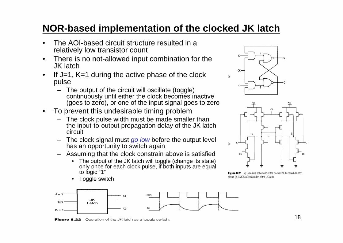
NOR-based implementation of the clocked JK latch• The AOI-based circuit structure resulted in a
relatively low transistor count• There is no not-allowed input combination for the
JK latch• If J=1, K=1 during the active phase of the clock
pulse– The output of the circuit will oscillate (toggle)
continuously until either the clock becomes inactive (goes to zero), or one of the input signal goes to zero
• To prevent this undesirable timing problem– The clock pulse width must be made smaller than
the input-to-output propagation delay of the JK latch circuit
– The clock signal must go low before the output level has an opportunity to switch again
– Assuming that the clock constrain above is satisfied• The output of the JK latch will toggle (change its state)
only once for each clock pulse, if both inputs are equal to logic “1”
• Toggle switch
19
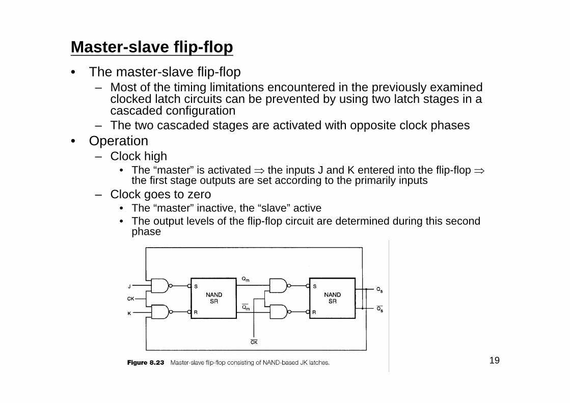
Master-slave flip-flop• The master-slave flip-flop
– Most of the timing limitations encountered in the previously examined clocked latch circuits can be prevented by using two latch stages in a cascaded configuration
– The two cascaded stages are activated with opposite clock phases• Operation
– Clock high• The “master” is activated ⇒ the inputs J and K entered into the flip-flop ⇒
the first stage outputs are set according to the primarily inputs– Clock goes to zero
• The “master” inactive, the “slave” active• The output levels of the flip-flop circuit are determined during this second
phase
20
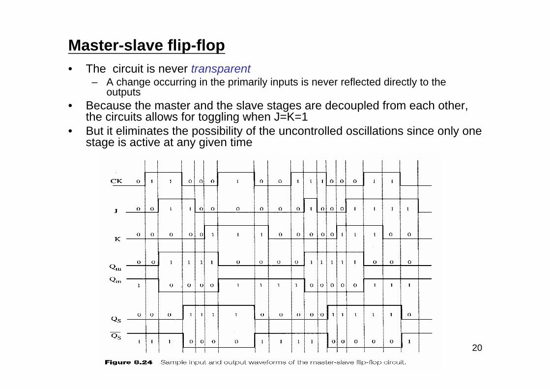
Master-slave flip-flop• The circuit is never transparent
– A change occurring in the primarily inputs is never reflected directly to the outputs
• Because the master and the slave stages are decoupled from each other, the circuits allows for toggling when J=K=1
• But it eliminates the possibility of the uncontrolled oscillations since only one stage is active at any given time
21
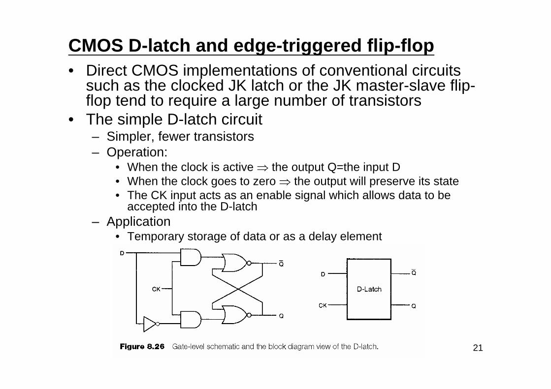
CMOS D-latch and edge-triggered flip-flop• Direct CMOS implementations of conventional circuits
such as the clocked JK latch or the JK master-slave flip-flop tend to require a large number of transistors
• The simple D-latch circuit– Simpler, fewer transistors– Operation:
• When the clock is active ⇒ the output Q=the input D• When the clock goes to zero ⇒ the output will preserve its state• The CK input acts as an enable signal which allows data to be
accepted into the D-latch– Application
• Temporary storage of data or as a delay element
22
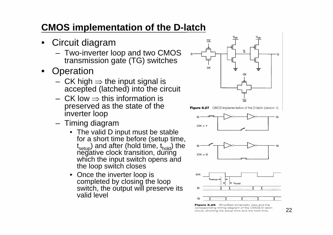
CMOS implementation of the D-latch• Circuit diagram
– Two-inverter loop and two CMOS transmission gate (TG) switches
• Operation– CK high ⇒ the input signal is
accepted (latched) into the circuit– CK low ⇒ this information is
preserved as the state of the inverter loop
– Timing diagram• The valid D input must be stable
for a short time before (setup time, tsetup) and after (hold time, thold) the negative clock transition, during which the input switch opens and the loop switch closes
• Once the inverter loop is completed by closing the loop switch, the output will preserve its valid level
23
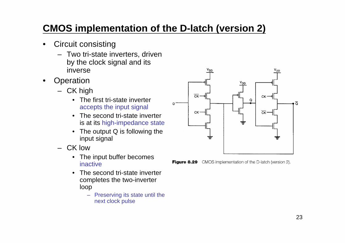
CMOS implementation of the D-latch (version 2)• Circuit consisting
– Two tri-state inverters, driven by the clock signal and its inverse
• Operation – CK high
• The first tri-state inverter accepts the input signal
• The second tri-state inverter is at its high-impedance state
• The output Q is following the input signal
– CK low• The input buffer becomes
inactive• The second tri-state inverter
completes the two-inverter loop
– Preserving its state until the next clock pulse
24
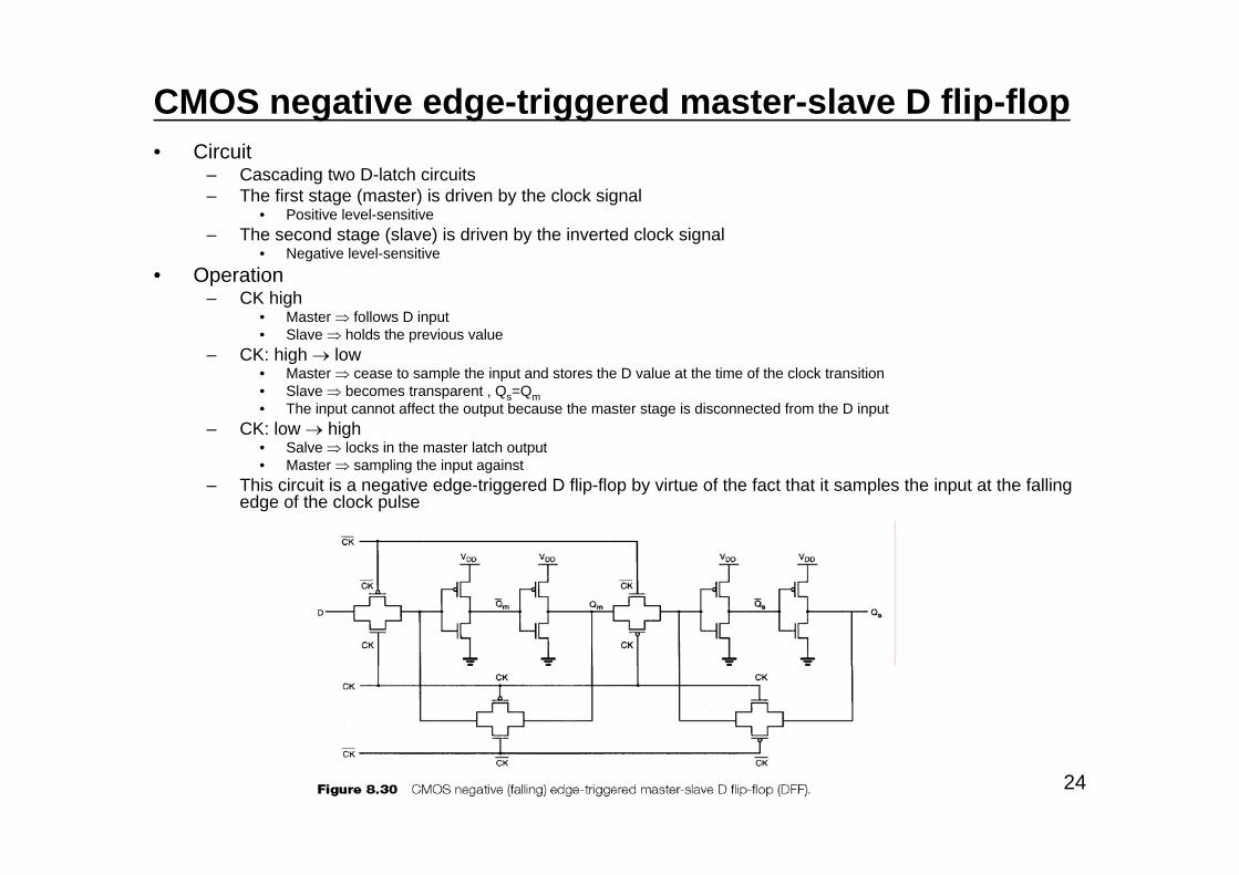
CMOS negative edge-triggered master-slave D flip-flop• Circuit
– Cascading two D-latch circuits– The first stage (master) is driven by the clock signal
• Positive level-sensitive– The second stage (slave) is driven by the inverted clock signal
• Negative level-sensitive• Operation
– CK high• Master ⇒ follows D input• Slave ⇒ holds the previous value
– CK: high → low• Master ⇒ cease to sample the input and stores the D value at the time of the clock transition• Slave ⇒ becomes transparent , Qs=Qm• The input cannot affect the output because the master stage is disconnected from the D input
– CK: low → high • Salve ⇒ locks in the master latch output• Master ⇒ sampling the input against
– This circuit is a negative edge-triggered D flip-flop by virtue of the fact that it samples the input at the falling edge of the clock pulse
25
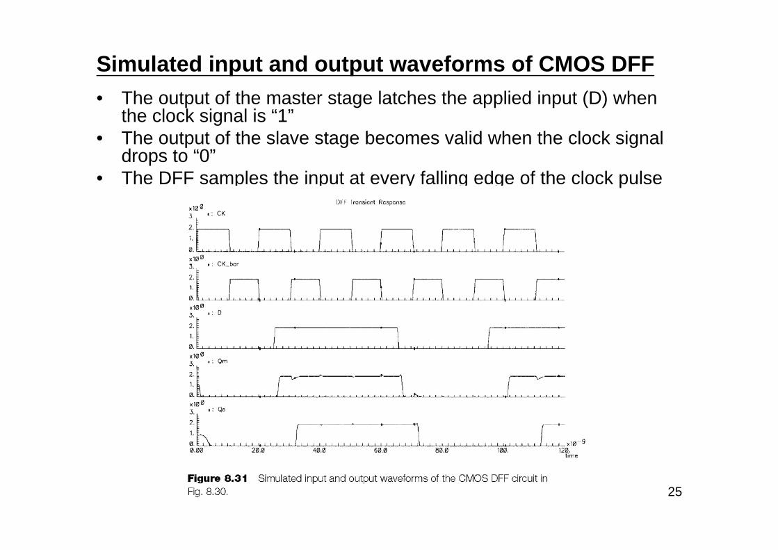
Simulated input and output waveforms of CMOS DFF• The output of the master stage latches the applied input (D) when
the clock signal is “1”• The output of the slave stage becomes valid when the clock signal
drops to “0”• The DFF samples the input at every falling edge of the clock pulse
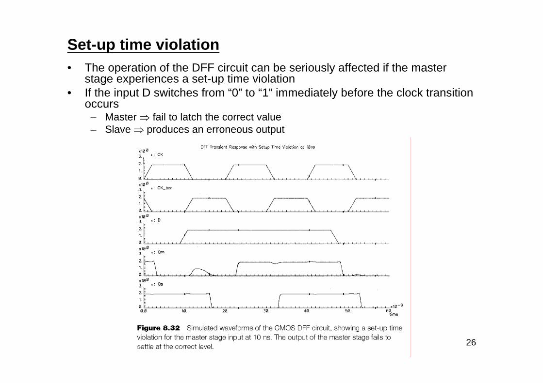
26
Set-up time violation• The operation of the DFF circuit can be seriously affected if the master
stage experiences a set-up time violation• If the input D switches from “0” to “1” immediately before the clock transition
occurs– Master ⇒ fail to latch the correct value– Slave ⇒ produces an erroneous output
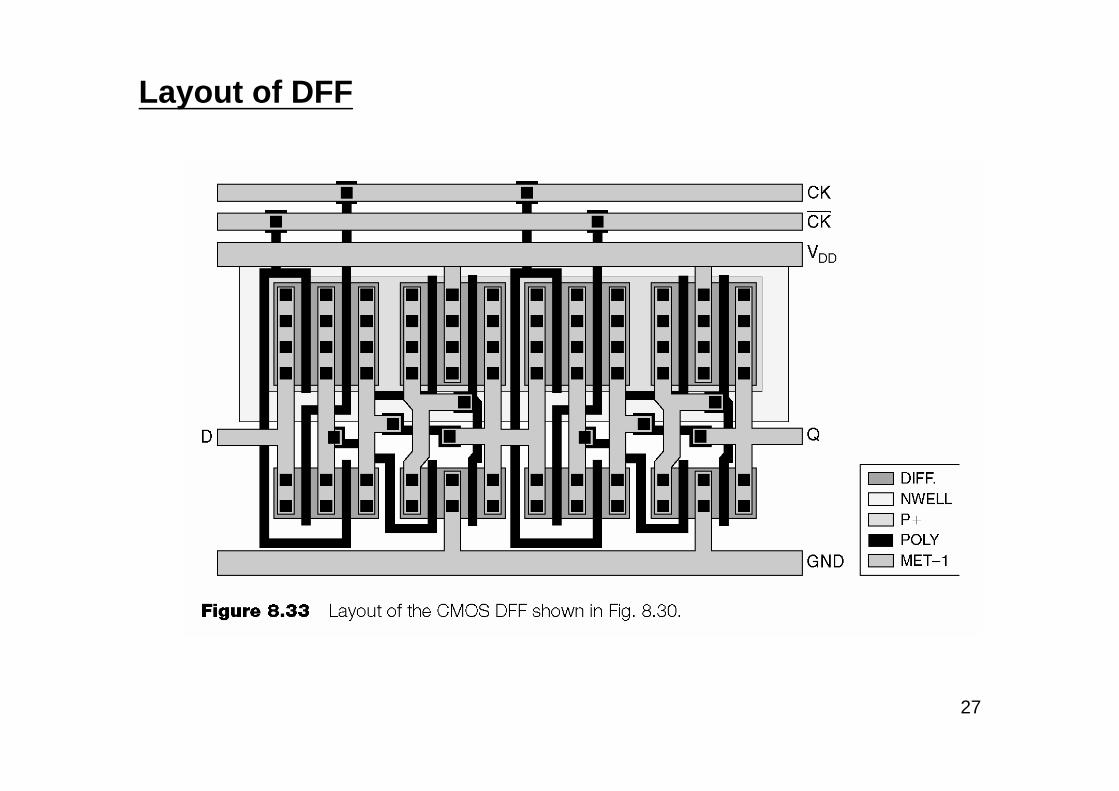
27
Layout of DFF
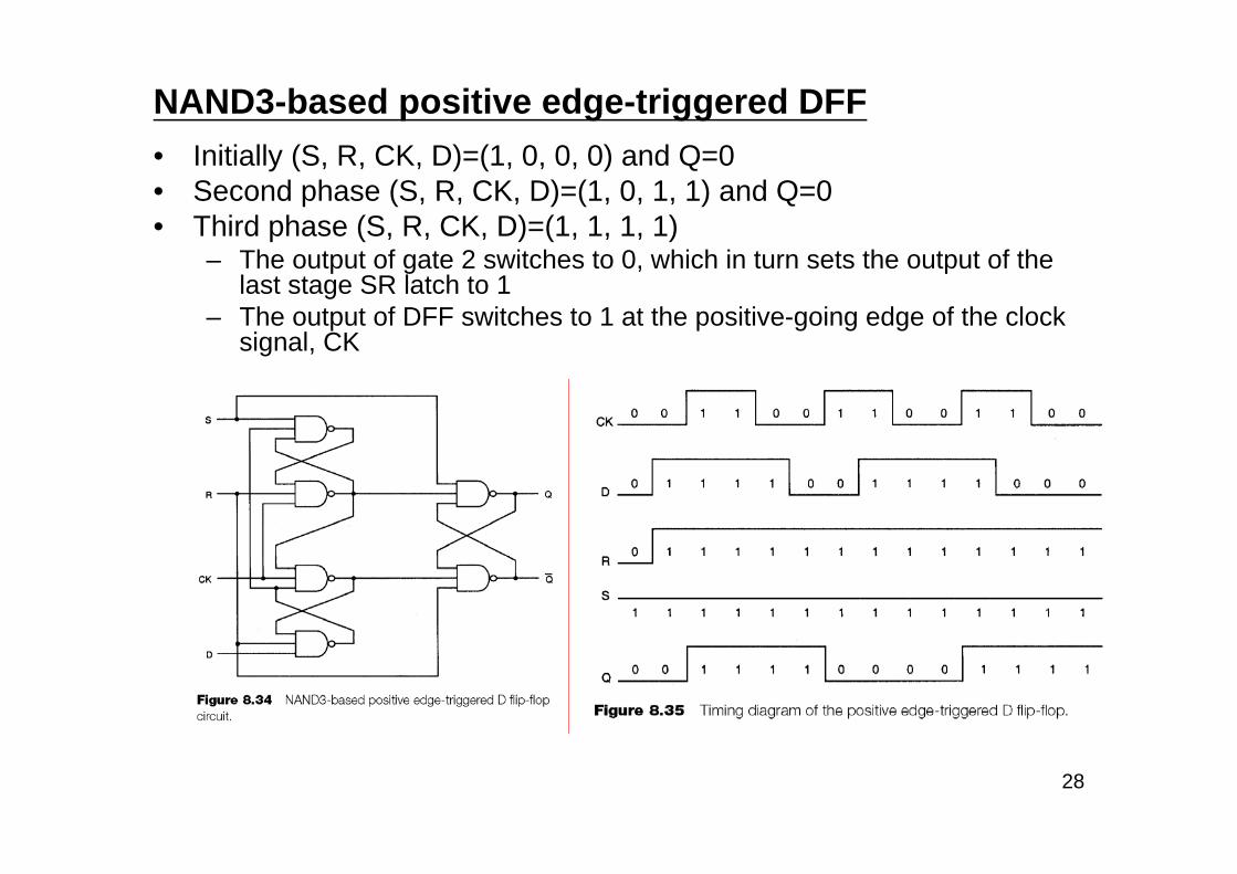
28
NAND3-based positive edge-triggered DFF• Initially (S, R, CK, D)=(1, 0, 0, 0) and Q=0 • Second phase (S, R, CK, D)=(1, 0, 1, 1) and Q=0 • Third phase (S, R, CK, D)=(1, 1, 1, 1)
– The output of gate 2 switches to 0, which in turn sets the output of the last stage SR latch to 1
– The output of DFF switches to 1 at the positive-going edge of the clock signal, CK
29
Schmitt trigger circuit
• A very useful regenerative circuit• The schmitt trigger
– Has an inverter-like voltage transfer characteristic
– With two different logic threshold voltages• For increasing input signal• For decreasing input signal
– Being utilized for the detection of low-to-high and high-to-low switching events in noisy environments
30
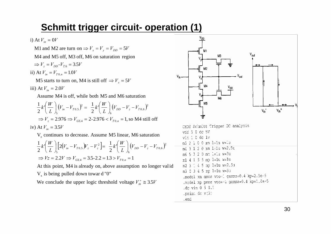
Schmitt trigger circuit- operation (1)
( ) ( )
( )[ ] ( )
V.V
V..-.VV.Vz
VVVL
Wk' VVVVL
Wk'
V.VV.-V.V
VVVL
Wk' VVL
Wk'
V.VVV
V.VVV.-VVV
VVVV
VV
th
,nTGS,
,TzDDzz,Tin
in
,nTGS,z
,TzDD,Tin
in
x
,nTin
T,DDz
DDyx
in
53 voltage thresholdlogicupper theconclude We
"0" ddown towar pulled being is V idlonger val no assumption above on,already is M4 point, At this
131225322212
21
saturation M6 linear, M5 Assume decrease. tocontinues V 53At iv)
off still M4 so ,197622976221
21
saturation M6 and M5both whileoff, is M4 Assume 02At iii)
5off still is M4 on, turn tostarts M5 01At ii)
53 region saturationon M6 off, M3 off, M5 and M4
5on turn are M2 and M1
0At i)
x
04
260
6
250
5
z
04
260
6
250
5
0
6
≅
=>==⇒=⇒
−−⎟⎠⎞
⎜⎝⎛=−−⎟
⎠⎞
⎜⎝⎛
=
=<=⇒=⇒
−−⎟⎠⎞
⎜⎝⎛=−⎟
⎠⎞
⎜⎝⎛
==⇒
==
==⇒
===⇒
=
+
31
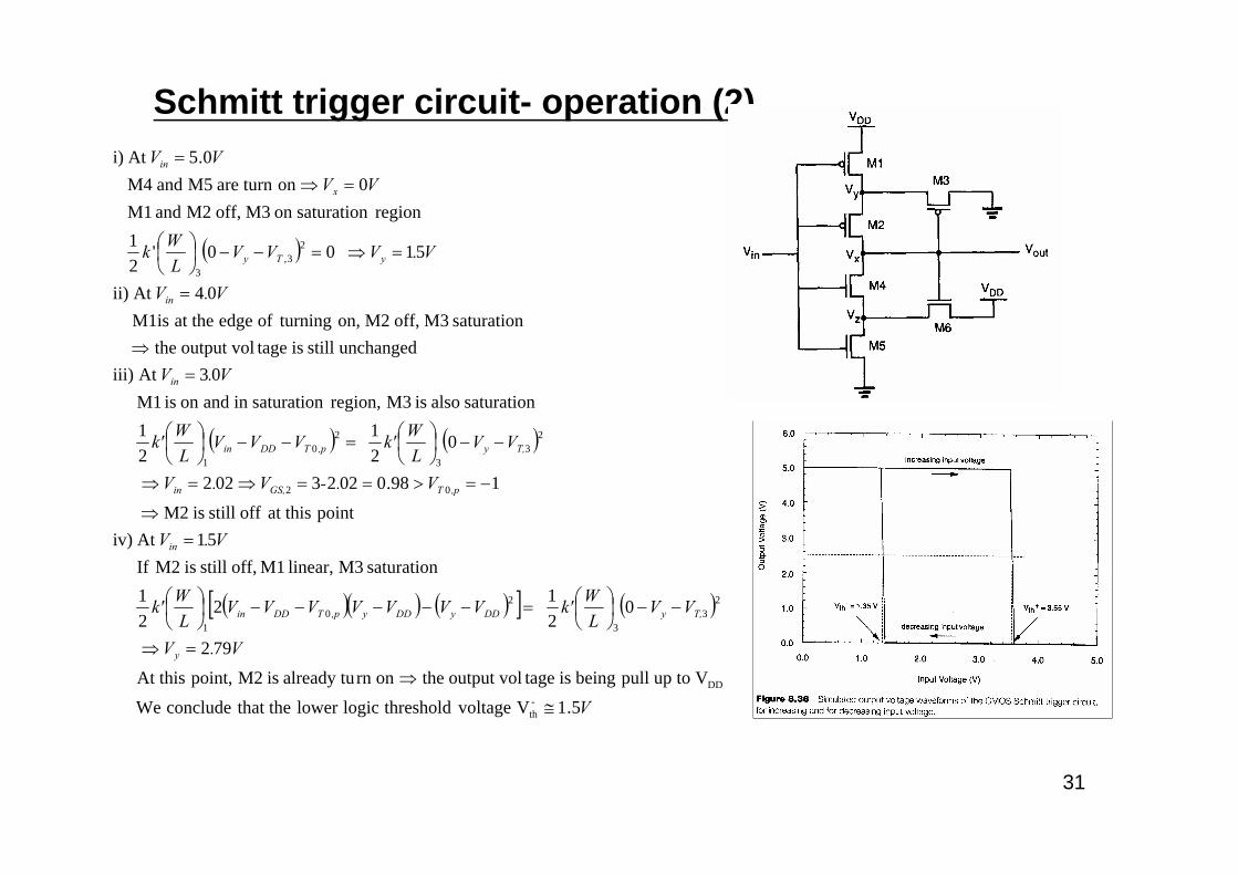
Schmitt trigger circuit- operation (2)
( )
( ) ( )
( )( ) ( )[ ] ( )
V
V.V
VVL
Wk' VVVVVVVL
Wk'
V.V
V.-V.V
VVL
Wk' VVVL
Wk'
V.V
V.V
V.VVVL
Wk
VVVV
y
T,yDDyDDy,pTDDin
in
,pTGS,in
T,y,pTDDin
in
in
yTy
x
in
5.1V voltage thresholdlogiclower that theconclude We
V toup pull being is tageoutput vol theonrn already tu is M2 point, At this
792
0212
21
saturation M3 linear, M1off, still is M2 If 51At iv)
point at this off still is M2
198.00223022
021
21
saturation also is M3 region, saturationin andon is M1 03At iii)
unchanged still is tageoutput vol the saturation M3 off, M2 on, turningof edge at the M1is
04At ii)
51 00'21
region saturationon M3 off, M2 and M1 0on turn are M5 and M4
0.5At i)
-th
DD
23
3
20
1
02
23
3
20
1
23,
3
≅
⇒
=⇒
−−⎟⎠⎞
⎜⎝⎛=−−−−−⎟
⎠⎞
⎜⎝⎛
=⇒
−=>==⇒=⇒
−−⎟⎠⎞
⎜⎝⎛=−−⎟
⎠⎞
⎜⎝⎛
=⇒
=
=⇒=−−⎟⎠⎞
⎜⎝⎛
=⇒=
Recommended