ANALYSIS, DESIGN AND IMPLEMENTATION OF ZERO-CURRENT-SWITCHING
RESONANT CONVERTER DC-DC BUCK CONVERTER
IRFAN JAMIL¹, ZHAO JINQUAN² & REHAN JAMIL³
1,2Department. of Energy & Electrical Engineering, Hohai University, Nanjing China
³Department. of Electrical Engr., Federal Urdu University of Arts, Science & Technology, Islamabad Pakistan
ABSTRACT
This paper presents a Buck type circuit structure, the designing of ZCS resonant Buck converter and analysis of the
working principles involved. The designed buck converter uses ZCS technique and the function is realized so that the
power form is converted from 12V DC to 5V DC (1A). A detailed analysis of zero current switching buck converters is
performed and a mathematical analysis of the mode of operation is also presented. In order to reduce the switching losses
in associated with conventional converters; resonant inductor and resonant capacitor (LC resonant circuit) is applied which
helps to turn on-off the switch at zero current. The dc-dc buck converter receives the energy from the input source, when
the switch is turned-on. If the switch is turned-off the LC resonant circuit pumps the energy by ensuring that the current
does not come to zero. During the hardware implementation Ton, Toff, duty cycle & operating frequency values were
determined and thoroughly tuned through the NE555 IC circuit. As a result of this various waveforms across capacitors,
inductors and load resistor were observed. A simulation study was carried out and the effectiveness of the designed
converter is verified by PSpice simulation results.
KEYWORDS: Dc-Dc Buck, ZCS, Resonant Converter, MOSFET, Timer, Simulation
INTRODUCTION
In recent years, with the state development of power electronic devices, development of control techniques and the
increasing demand of high-quality power supply, power electronics technology has invoked widely attention from research
scholars over the world. Power electronics technology has been gradually taken up in civilian industrial areas to cope with
these demands. The various converters for different requirements are developed and related technology is studied by
scientists to accomplish the research of new converters.
This work focuses on the issues related with the designing of ZCS buck converter. The main objective of the work
is to append zero current switching techniques, LC Resonant circuits and buck topology. There is major requirement for
changing the voltage from one level to another. Dc-dc converters can be utilized for this purpose because they efficiently
change the dc electrical power into a different impedance level [2]. Buck converters are one of the most important
components of the circuit which operates the voltage from the desired level to fixed level [10].
The dc-dc buck converter is a step down converter, if the energy is received from input source while switch is
turned-on. And if the switch is turned-off the LC resonant circuit (referred to as the “Tank Circuit”) pumps the energy by
ensuring that the current does not reach to zero. When the inductor current hits zero, the switch engages. Hence, it is
referred to as Zero current switching. The Quasi Resonant converter can be considered as combination of resonant
switching & PWM switching. The resulting hybrid converter combines the properties of a resonant switch network and a
conventional PWM converter. It consists of the switch MOSFET and LC Resonant Circuit (Tank Circuit) [12].
International Journal of Electrical and
Electronics Engineering (IJEEE)
ISSN 2278-9944
Vol. 2, Issue 2, May 2013, 1-12
© IASET

2 Irfan Jamil, Zhao Jinquan & Rehan Jamil
This paper also deals with a simple buck converter topology with switching resonant element MOSFET. It is
switched on and off using a 555 NE timer with switching frequency of 42KHZ. The converter is operating with Input
source of 12Vdc which provides a regulated output voltage of 5Vdc (1 A). The operating principle of the converter
topology is analyzed and operating modes are studied [13]. The performance of the ZCS buck converter is recorded and
examined for theoretical verification, waveform results and pspice simulation.
Figure 1: Block Diagram of Proposed Converter
REASONANT CONVERTER
The converters which employ ZC and/or ZV switching technique are usually called resonant converters. The
resonant converters were investigated in early 1980s as they can achieve very low switching loss thus enabling the resonant
topologies to work with a high switching frequency. In these converters, some form of L-C resonance is used, which is
why they are known as resonant converters [1]. Resonant converters are repelled or driven with constant pulse duration at a
variable frequency to maintain control over output voltage. The pulse duration is required to be equal to half of the time of
resonant period for switching at the zero current or voltage crossing points. The resonant converters contain the serial or
parallel connections of inductors and capacitors to enable the switch to achieve the ZCS & ZVS under resonance
conditions, the result effects switching losses, switching stress and EMI problems [3], [5], [7], [15]. The switching resonant
converter controls the output voltage through switching frequency, and generally can be sub-classified in ZCS Converter
and ZVS Converter [5]. There are many variations that can be placed at the primary or secondary side of the transformer
and alternatively called serial or parallel resonant circuit which indicates whether it is required to turn off the transistor
when current or voltage is zero. So far these are distinguished as ZVS and ZCS resonant converters. Resonant converts are
combination of converter topologies or switching strategies that in consequence produce zero voltage and/or zero current
switching.
Zero Current Switching Technique
In switching technique, the mainly research carried out thus for pertains to hard switching and soft switching
techniques. Hard switching technique relates to the stressful switching behaviors of power electronics devices whilst soft
switching techniques are applied to eliminate the harmful effects of hard switching. Therefore soft switching techniques
are more significantly developed and are normally applied to reduce the problems of switching losses in dc-dc power
converters operating with high switching frequency [3], [5], [7].
Generally there are two types of techniques known as Zero-current switching (ZCS) and Zero-Voltage Switching
(ZVS) which are called conventionally employed soft-switching methods [11].When the switch current is reached to zero
at the switching instants, it is usually known as Zero-Current switching (ZCS) and if certainly the switch voltage is reached
to zero at switching instants, it is usually known as Zero-voltage switching (ZVS). The main difference between the two is
to do with when the switching occurs [8].
Analysis, Design and Implementation of Zero-Current-Switching 3 Resonant Converter DC-DC Buck Converter
The ZCS is a type of soft switching technique which was first proposed by F C Y Lee al (1987) [12]. Reducing
stress on the switching components is a major incentive for resonant operation; and we need to understand ways through
which that might be fulfilled. The simplest approach and the one to which most of this paper presents ZCS operation of a
converter switch must be such that involves the current flowing through the switch being induced to rise gradually just
after the switch is turned-on so that it has a ZCS turn-on. The switch current must also be induced to descend gradually just
before the switch is turned-off so that it can have a ZCS turn-off. The ZCS turn-on feature of a converter switch can be
made certain by simply connecting an inductor in series as the current flowing through an inductor cannot change
immediately. Connecting an inductor in series with a switch also ensures that the current flowing through the other devices
in the converter is gradually drawn back so that they can turn-off with ZCS. The ZCS turn-off of a converter switch can be
made certain by providing another path for the current to flow through, just before the switch is turned off. Since the
switch has a relatively small voltage drop, the other path must be at a lower voltage potential so that current can be turned
away from the switch [4].
CIRCUIT ANALYSIS DESCRIPTION
The Dc-Dc buck converter has simple principle of operation in family of converters. However circuit analysis of
buck converter has widely related to discussions of topology with ZCS resonant converters in power electronics.
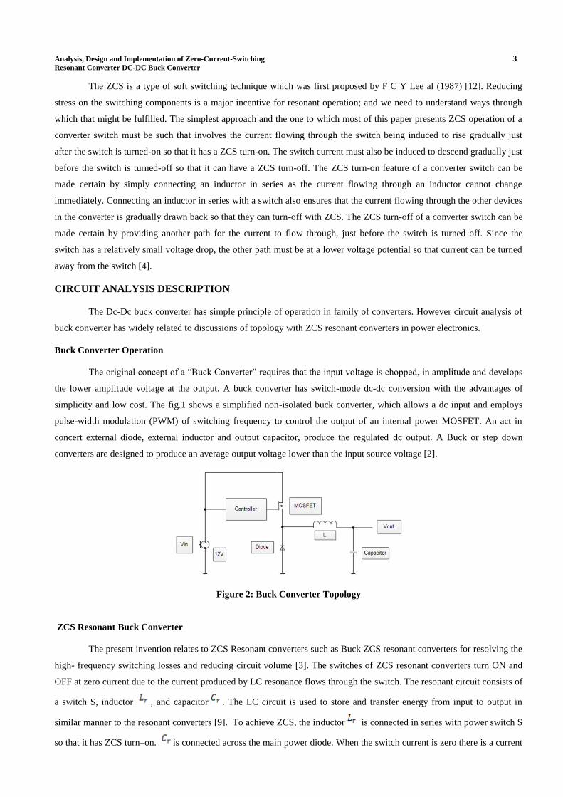
Buck Converter Operation
The original concept of a “Buck Converter” requires that the input voltage is chopped, in amplitude and develops
the lower amplitude voltage at the output. A buck converter has switch-mode dc-dc conversion with the advantages of
simplicity and low cost. The fig.1 shows a simplified non-isolated buck converter, which allows a dc input and employs
pulse-width modulation (PWM) of switching frequency to control the output of an internal power MOSFET. An act in
concert external diode, external inductor and output capacitor, produce the regulated dc output. A Buck or step down
converters are designed to produce an average output voltage lower than the input source voltage [2].
Figure 2: Buck Converter Topology
ZCS Resonant Buck Converter
The present invention relates to ZCS Resonant converters such as Buck ZCS resonant converters for resolving the
high- frequency switching losses and reducing circuit volume [3]. The switches of ZCS resonant converters turn ON and
OFF at zero current due to the current produced by LC resonance flows through the switch. The resonant circuit consists of
a switch S, inductor , and capacitor . The LC circuit is used to store and transfer energy from input to output in
similar manner to the resonant converters [9]. To achieve ZCS, the inductor is connected in series with power switch S
so that it has ZCS turn–on. is connected across the main power diode. When the switch current is zero there is a current

4 Irfan Jamil, Zhao Jinquan & Rehan Jamil
flowing through the internal capacitance due to finite slope of switch voltage at turn off. This current flow causes power
dissipation in the switch and sets the high switching frequency [11]. In ZCS techniques, the turn off losing of switching
devices are almost eradicated. Therefore the converter can be functioned at higher frequencies, in the range of 1MHz to
2MHz. The advantages of Buck ZCS resonant converter that they have low switching losses due to resonance techniques,
easy drive on switches and low stress on switching elements (MOSFET) as well [14].
Figure 3: ZCS Reasonant Buck Converter
Mode 1 Mode 2
Mode 3 Mode 4
Mode 5
Figure 4: Equivalent Mode of ZCS Reasonant Buck Converter
Analysis Mode of Operation
The circuit discussions are made on Half-wave mode of operations which can be divided into 5 operating modes.
The circuit operates in the half-wave mode if the switch is unilateral which means there is no antiparallel diode across the

Analysis, Design and Implementation of Zero-Current-Switching 5 Resonant Converter DC-DC Buck Converter
switch S. if the switch is bilateral that means the diode is available across the switch S and it works in full-wave mode [14].
Assume the time origin, t=0, at the beginning of each mode. We operate from a regulated DC voltage supply = 12V,
Assuming that a purely resistive load is used approximate current flowing through the load resistance is obtained as: =
12/90=0.133A. Resonant inductor = 2µH, Resonant capacitor =( )= 1.32µF , = 90K
Mode 1 (0≤t≤ ): When the switch (S) is turned-on at t=0, the current through the resonant inductor which
rises linearly from zero is given by
= t (1)
The remainder of and flows through ( = - ). The voltage across C remains zero during the entire
conduction period of . When = , then becomes zero and turns off when this mode ends at t= .
∴ = , = 0 , (2)
(3)
Mode 2 (0≤t≤ ): In this mode, switch (S) remains ON but diode is OFF. When the diode ( ) current reduces
to zero, the resonant capacitor is charged resonantly by a current - ).
The inductor current is given by
Where = + sin t (4)
= (5)
= (6)
The capacitor voltage is given by
= (1- ) (7)
The peak current which occurs at
t = is given by (8)
= + (9)
The peak capacitor voltage is given by
= (10)
Condition for current zero switching is
≤ (11)
6 Irfan Jamil, Zhao Jinquan & Rehan Jamil
This mode ends at t= when =
Therefore = π => (12)
Mode 3 (0≤t≤ ): At time t= , During this mode, the voltage across capacitor and current through the inductor
are given by
The inductor current is
= - (13)
The capacitor voltage is given by
= . (14)
This mode ends at (t= ) , when =0 and =
Thus From the eq. (13)
= or (15)
= (16)
(17)
Mode 4 (0≤t≤ ): At time t= , The switch is OFF during this period. The capacitor commences to discharge
through the output with constant output current ( ) and which decreases linearly.
The capacitor supplies load current and thus the capacitor voltage is given by
= - t (18)
This mode ends at t= when = 0
From above equation (18)
= (19)
(20)
Mode 5 (0≤t≤ ): In this mode, at the beginning of period, tends to be negative due to the resonating,
circuit. Therefore conducts and the load current flows through . The peak resonating current must be
higher than for a half-wave ZCS converter. This mode ends at time t = when the switch (S) is turned-on again and
the next cycle starts. Thus, the cycle is repeated which means that = T- ( + + + ).
For the sake of simplicity we assume

Analysis, Design and Implementation of Zero-Current-Switching 7 Resonant Converter DC-DC Buck Converter
Therefore (21)
(22)
(23)
(24)
Duty ratio (25)
Frequency of operation (26)
DESIGN CONSIDERATION
The ZCS buck converter design consists chiefly of two parts. One is power the circuit and the other is the control
circuit. The power and control circuits are designed with following specifications.
Table 1: ZCS Buck Converter
Parameters Values
Input 12V
Output 5V, 1A, 5W
Resonant Inductor 2µH
Resonant Capacitor 1.32µF
Mosfet NR411
Switching Frequency 42KHZ
Topology Isolated Buck Converter
Controller NE 555 Timer
Output Resistor 90K
In circuit description, resonant inductor and resonant capacitor are formed by a LC resonant pair which is used to
generate the resonance. This pair is produced via sinusoidal waveforms from the dc input. The diode operates that blocks
the negative half cycle of generated from the LC resonant pair. The LC filter is used to smooth the waveforms which
eliminate harmonics, ripples and noise. In this circuit the topology used is an isolated buck converter & controller timer
NE555 timer (Control circuit) which controls the switching element MOSFET IRFZ44 (Power circuit). For ZCS operation,
the ON time is fixed and the frequency variation is achieved by varying the OFF time only. For the 555 Timer, the ON
time and OFF time equation is given,
= 0.693[ + ] ( = 20K, =47K, = 1nF)
=0.693[ ]
The switching frequency is varied at 42 KHz and variation is done by ensuring a Trim pot and a diode in
parallel across to bypass the resistor during the ON time. The ON time is set to be 3.6µs and , & are calculated
from the above equation.
For zero- current switching,
= = 9.748
8 Irfan Jamil, Zhao Jinquan & Rehan Jamil
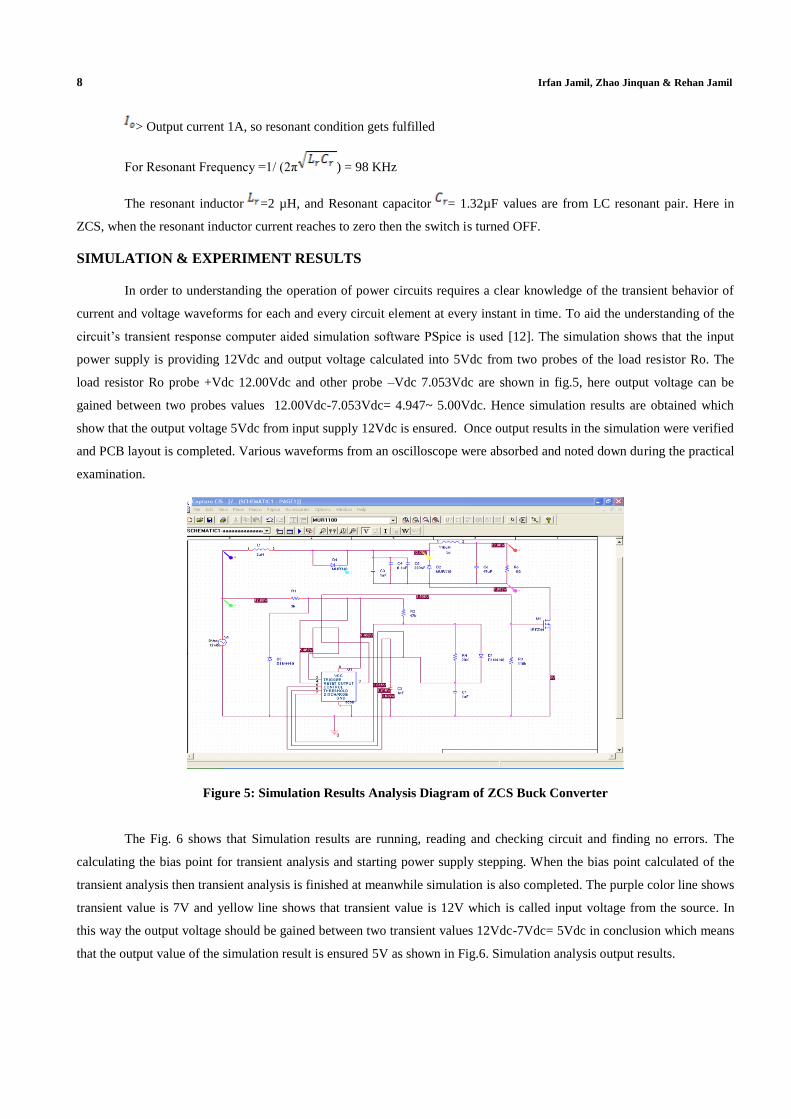
> Output current 1A, so resonant condition gets fulfilled
For Resonant Frequency =1/ (2π ) = 98 KHz
The resonant inductor =2 µH, and Resonant capacitor = 1.32µF values are from LC resonant pair. Here in
ZCS, when the resonant inductor current reaches to zero then the switch is turned OFF.
SIMULATION & EXPERIMENT RESULTS
In order to understanding the operation of power circuits requires a clear knowledge of the transient behavior of
current and voltage waveforms for each and every circuit element at every instant in time. To aid the understanding of the
circuit’s transient response computer aided simulation software PSpice is used [12]. The simulation shows that the input
power supply is providing 12Vdc and output voltage calculated into 5Vdc from two probes of the load resistor Ro. The
load resistor Ro probe +Vdc 12.00Vdc and other probe –Vdc 7.053Vdc are shown in fig.5, here output voltage can be
gained between two probes values 12.00Vdc-7.053Vdc= 4.947~ 5.00Vdc. Hence simulation results are obtained which
show that the output voltage 5Vdc from input supply 12Vdc is ensured. Once output results in the simulation were verified
and PCB layout is completed. Various waveforms from an oscilloscope were absorbed and noted down during the practical
examination.
Figure 5: Simulation Results Analysis Diagram of ZCS Buck Converter
The Fig. 6 shows that Simulation results are running, reading and checking circuit and finding no errors. The
calculating the bias point for transient analysis and starting power supply stepping. When the bias point calculated of the
transient analysis then transient analysis is finished at meanwhile simulation is also completed. The purple color line shows
transient value is 7V and yellow line shows that transient value is 12V which is called input voltage from the source. In
this way the output voltage should be gained between two transient values 12Vdc-7Vdc= 5Vdc in conclusion which means
that the output value of the simulation result is ensured 5V as shown in Fig.6. Simulation analysis output results.

Analysis, Design and Implementation of Zero-Current-Switching 9 Resonant Converter DC-DC Buck Converter
Figure 6: Simulation Analysis Output Results
Fig. 7 shows that output voltage 5Vdc is constant for particular 42 KHz switching frequency. The output voltage
can be controlled via switching frequency [5]. If switching frequency increases then output voltage will also increase. In
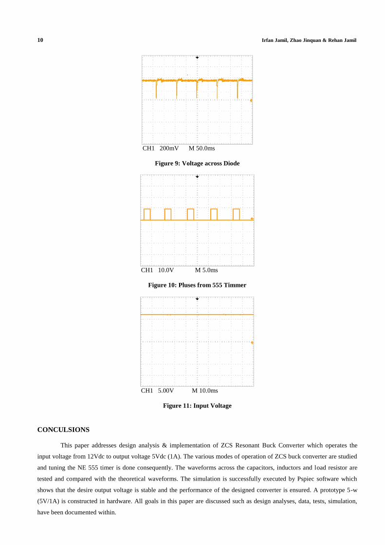
other figures (Fig. 8, Fig. 9, Fig. 10 and Fig. 11 respectively) the waveforms results were absorbed.
CH1 5.00V M 10.0ms
Figure 7: Output Voltage
CH1 5.00V M 10.0ms
Figure 8: Voltage across Resistor & Capacitor
10 Irfan Jamil, Zhao Jinquan & Rehan Jamil
CH1 200mV M 50.0ms
Figure 9: Voltage across Diode
CH1 10.0V M 5.0ms
Figure 10: Pluses from 555 Timmer
CH1 5.00V M 10.0ms
Figure 11: Input Voltage
CONCULSIONS
This paper addresses design analysis & implementation of ZCS Resonant Buck Converter which operates the
input voltage from 12Vdc to output voltage 5Vdc (1A). The various modes of operation of ZCS buck converter are studied
and tuning the NE 555 timer is done consequently. The waveforms across the capacitors, inductors and load resistor are
tested and compared with the theoretical waveforms. The simulation is successfully executed by Pspiec software which
shows that the desire output voltage is stable and the performance of the designed converter is ensured. A prototype 5-w
(5V/1A) is constructed in hardware. All goals in this paper are discussed such as design analyses, data, tests, simulation,
have been documented within.

Analysis, Design and Implementation of Zero-Current-Switching 11 Resonant Converter DC-DC Buck Converter
ACKNOWLEDGEMENTS
The authors would like to acknowledge financial support from College of Engineering and College of
International Education, Hohai University.
REFERENCES
1. Shahab Ahmad and K.P.Singh “Simulation of Step-Down/Step-Up Converter Implemented with ZCS Soft
Switching” VSRD-IJEECE, Vol.2 (9), pp 695-704, 2012.
2. Vaman B Gudil, Dr. H N Nagaraj, Dr. Paramesh, Basavaraj V Madiggond “Design Issues in Single Stage
Synchronous Buck Converter” International Journal Of Emerging Technology and Advanced Engineering Vol. 2,
Issue 4, April 2012.
3. Yu-Lung Ke, Ying-Chun Chuang, Shao-Wei Huang “Application of Buck Zero-Current-Switching Pluse-Width-
Modulated Converter in Battery Chargers” Industrial and Commercial Power Systems Technical Conference 2007.
4. Sondeep Bassan and Gerry Moschopoulos “Zero-Current-Switching Techniques for Buck-Type AC-DC
Converters” Telecommunications Energy International Conference - INTELEC , 2007.
5. Naseem Zaidi, Aziz Ahmad “ Anaylsis, Design and Control of Zero Current Switching DC To DC Buck
Converter” International Journal of Scientific and Research Publications, Vol. 2, Issue 7, July 2012.
6. V,Grigone, J . Kyyra “A 500W (50V @10A) ZVT Forward Converter” in Proceedings of the 13th IEEE Applied
Power Electronics Conference, APEC'98, Anaheim, CA, USA, 1998, pp. 614-619.
7. Helio Leaes Hey, Lourenco Matias and Joao Batista Viera Junior “A Buck ZC-ZVS PWM Converter” Power
Electronics Specialists Conference PESC '94 Record. 25th Annual IEEE June 1994.
8. A. Emrani, H. Farzanehfard “ A New Zero Current Switching Resonant Buck Converter “the 24th Canadian
Conference on Electrical and Computer Engineering, CCECE 2011, Niagara Falls, Ontario, Canada, 8-11 May,
2011.
9. Ivo Barbi, Julio C. O. Bolacell, Denizar C. Martins, Fausto B. Libano, “Buck Quasi-Resonant Converter
Operating at Constant Frequency: Analysis, Design, and Experimentation” IEEE Transactions on Power
Electronic. Vol. 5. NO. 3, July 1990.
10. Nanda R Mude, Prof. Ashish Sahu, “Adaptive Control Schemes For DC-DC Buck Converter” International
Journal Of Engineering Research and Application Vol. 2, Issue 3, PP. 463-467, May-Jun 2012.
11. Ying-Chun Chuang, “High-Efficiency ZCS Buck Converter for Rechargeable Batteries” IEEE Transactions on
Industrial Electronics, Vol. 57, NO. 7, July 2010.
12. K. Narasimha Rao, Dr V.C. Verra Reddy, “Implementation of FM-ZCS-Quasi Resonant Converter Fed DC Servo
Drive” Journal of theoretical and applied Information Technology, In Proceedings of the Second International
Conference on Emerging Trends in Engineering & Technology, ICETET 2009.
13. P.Hemachander, Dr.P.Ajay-DVimalRaj, Dr.M.Sudhakaran,“Analysis Design and Implementation of Soft Single
Switched Boost Converter” International Journal of Computer Application Vol. 26- No.11, July 2011.
12 Irfan Jamil, Zhao Jinquan & Rehan Jamil
14. M.D Singh, K B Khanchandani, Electrical & Electronics Engineering series, 2rd ed., TATA McGraw-Hill, 2008,
pp.775-778.
15. Y.C. Chuang, Y.-L. Ke, “High Effieceny battery charger with a buck zero-current-switching pulse-width-
modulated converter” IET Power Electron., 2008, Vol. 1, No.4, pp. 433-444.
AUTHOR’S DETAILS
Irfan Jamil was born in Punjab province, City Multan, Pakistan on Feb 25, 1987. He received his bachelor
degree in Electrical Engineering and its Automation from Harbin Engineering University, Harbin, China in 2011. Currently
he is pursuing his Master degree at Hohai University, Nanjing, China. During these days he is doing master research as a
Visiting Research Scholar at Tsinghua University, Beijing China. His research interest involves in Power electronics and
Power system Automation.
Rehan Jamil was also born in Punjab province, City Multan, Pakistan on Feb 25, 1987. He received his bachelor
in B.Sc. Electrical (Electronic) Engineering from Federal Urdu University of Arts, Science & Technology, and Islamabad
Pakistan in 2009. Currently he is pursuing his Master degree at Yunnan Normal University, Kunming China. His research
interest involves in Electronics, Renewable energy power generation.
Prof. Jinquan Zhao was born in Yangquan, Shanxi province, China, on June 26 1972. He received B.S. and
Ph.D. degrees, all in electrical engineering, from Shanghai Jiao tong University, Shanghai, China, in 1993 and 2000,
respectively. From 1993 to 1995, he was an engineer in Guangzhou Power Company, Guangzhou, China. From December
2000 to September 2003, he was a postdoctoral associate in Cornell University, Ithaca, NY. He was a postdoctoral
associate in Tsinghua University, Beijing, China. Currently he is a professor in Electrical Engineering department, Hohai
University, Nanjing, China. He has been published more than 28 papers in many international conferences. His research
interests in the area of voltage stability analysis and control, OPF and its applications.
Recommended