PLUS+1™ Inverters
Data sheet 70300001 V1.4
Data sheet for PLUS+1™ Inverters
70300001 V1.4 – June 2012 2/13
Versions
Version HistoryVersion HistoryVersion HistoryVersion History Table of Versions
DateDateDateDate PagePagePagePage DescriptionDescriptionDescriptionDescription VersionVersionVersionVersion
08.09.2010 All Complete rework of old document, new format,
change over to Versions
1.0
27.01.2010 All MIxx-X1 added 1.1
09.02.2011 3, 5, 9 Status update availability
Remark added, that “sensor supply” for MIxx-X1 has
a constant value.
1.2
22.03.2012 2 MI08 updated after development / MI14 deleted 1.3
20.06.2012 2, 4, 5 MI08 update after release, Legend update page 2/4
new pages 4/5 was former page 10
1.4
2 New words for nominal, maximum, peak current
Schwarzmüller Inverter welcomes suggestions to improve our documentation. If you have suggestions for improving this document, please contact Schwarzmüller Inverter at [email protected].
© 2011, Schwarzmüller Inverter Schwarzmüller Inverter can accept no responsibility for possible errors in catalogs, brochures and other printed material. Schwarzmüller Inverter reserves the right to alter its products without prior notice. This also applies to products already ordered provides that such alterations can be made without affecting agreed specifications. All trademarks in this material are properties of the respective owners. Sauer-Danfoss ,the Sauer-Danfoss logotype, the Sauer-Danfoss S-icon, PLUS+1TM, what really matters is inside® and Know-How in MotionTM are trademarks of the Sauer-Danfoss Group.
Data sheet for PLUS+1™ Inverters
70300001 V1.4 – June 2012 3/13
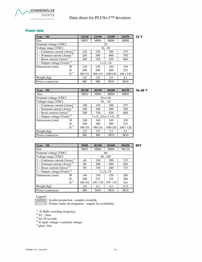
Power dataPower dataPower dataPower data
24 V
36-48 V
80V
Legend: xx/yyy
xx/yyy In pilot production - samples available
Product under development – require for availability
1) @ 8kHz switching frequency 2)
S2 - 2min 3)
for 10 seconds 4)
@ input voltage = nominal voltage 5) plate / fins
Type: MI- 24/240 24/300 24/400 24/550
Size MI03 MI04 MI06 MI08
Nominal voltage [VDC] 24
Voltage range [VDC] 16...36
3 ~ Continous current [Arms] 1)
120 150 200 275
3 ~ Nominal current [Arms] 2)
240 300 400 550
3 ~ Boost current [Arms] 3) 260 330 420 600
3 ~ Output voltage [Vrms] 4)
3 x 0...16
Dimensions [mm] W
H
D 5)
140
200
90/110
140
200
90/110
140
200
100/120
150
225
100 / 120
Weight [kg] 2,8 3,0 3,5 4,1
Power connectors M6 M8 M10 M10
Type: MI- 48/180 48/300 48/400 48/550
Size MI03 MI04 MI06 MI08
Nominal voltage [VDC] 36 or 48
Voltage range [VDC] 18 ... 62
3 ~ Continous current [Arms] 1)
100 150 200 275
3 ~ Nominal current [Arms] 2)
180 300 400 550
3 ~ Boost current [Arms] 3) 200 330 420 600
3 ~ Output voltage [Vrms] 4)
3 x 0...24 or 3 x 0...32
Dimensions [mm] W
H
D 5)
140
200
90/110
140
200
90/110
140
200
100/120
150
225
100 / 120
Weight [kg] 2,8 3,0 3,5 4,1
Power connectors M6 M8 M10 M10
Type: MI- 80/80 80/300 80/400 80/650
Size MI03 MI08 MI08 MI-20
Nominal voltage [VDC] 80
Voltage range [VDC] 40...105
3 ~ Continous current [Arms] 1)
40 150 200 325
3 ~ Nominal current [Arms] 2)
80 300 400 650
3 ~ Boost current [Arms] 3) 90 330 440 715
3 ~ Output voltage [Vrms] 4)
3 x 0...53
Dimensions [mm] W
H
D 5)
140
200
90/110
150
225 100 / 120
150
225 100 / 120
280
280
141
Weight [kg] 2,8 4,1 4,1 11,5
Power connectors M6 M10 M10 M10
Data sheet for PLUS+1™ Inverters
70300001 V1.4 – June 2012 4/13
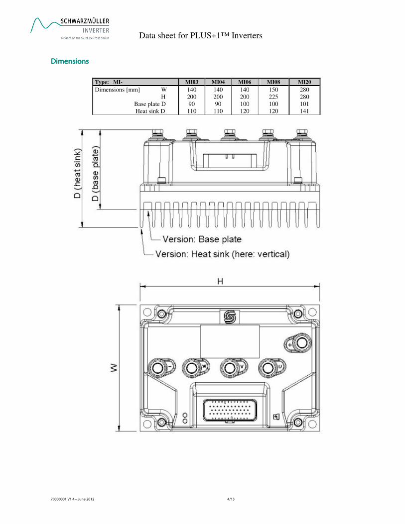
DimensionsDimensionsDimensionsDimensions
Type: MI- MI03 MI04 MI06 MI08 MI20
Dimensions [mm] W
H
Base plate D
Heat sink D
140
200
90
110
140
200
90
110
140
200
100
120
150
225
100
120
280
280
101
141
Data sheet for PLUS+1™ Inverters
70300001 V1.4 – June 2012 5/13
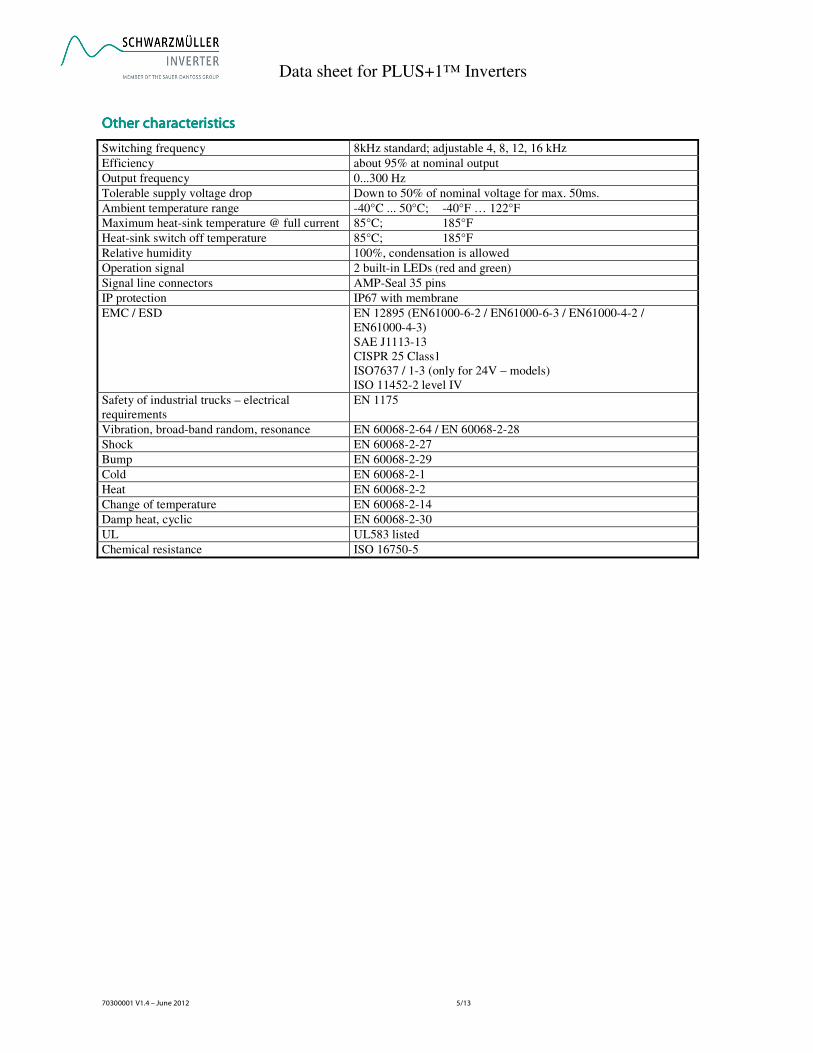
Other characteristicsOther characteristicsOther characteristicsOther characteristics
Switching frequency 8kHz standard; adjustable 4, 8, 12, 16 kHz
Efficiency about 95% at nominal output
Output frequency 0...300 Hz
Tolerable supply voltage drop Down to 50% of nominal voltage for max. 50ms.
Ambient temperature range -40°C ... 50°C; -40°F … 122°F
Maximum heat-sink temperature @ full current 85°C; 185°F
Heat-sink switch off temperature 85°C; 185°F
Relative humidity 100%, condensation is allowed
Operation signal 2 built-in LEDs (red and green)
Signal line connectors AMP-Seal 35 pins
IP protection IP67 with membrane
EMC / ESD EN 12895 (EN61000-6-2 / EN61000-6-3 / EN61000-4-2 /
EN61000-4-3)
SAE J1113-13
CISPR 25 Class1
ISO7637 / 1-3 (only for 24V – models)
ISO 11452-2 level IV
Safety of industrial trucks – electrical
requirements
EN 1175
Vibration, broad-band random, resonance EN 60068-2-64 / EN 60068-2-28
Shock EN 60068-2-27
Bump EN 60068-2-29
Cold EN 60068-2-1
Heat EN 60068-2-2
Change of temperature EN 60068-2-14
Damp heat, cyclic EN 60068-2-30
UL UL583 listed
Chemical resistance ISO 16750-5
Data sheet for PLUS+1™ Inverters
70300001 V1.4 – June 2012 6/13
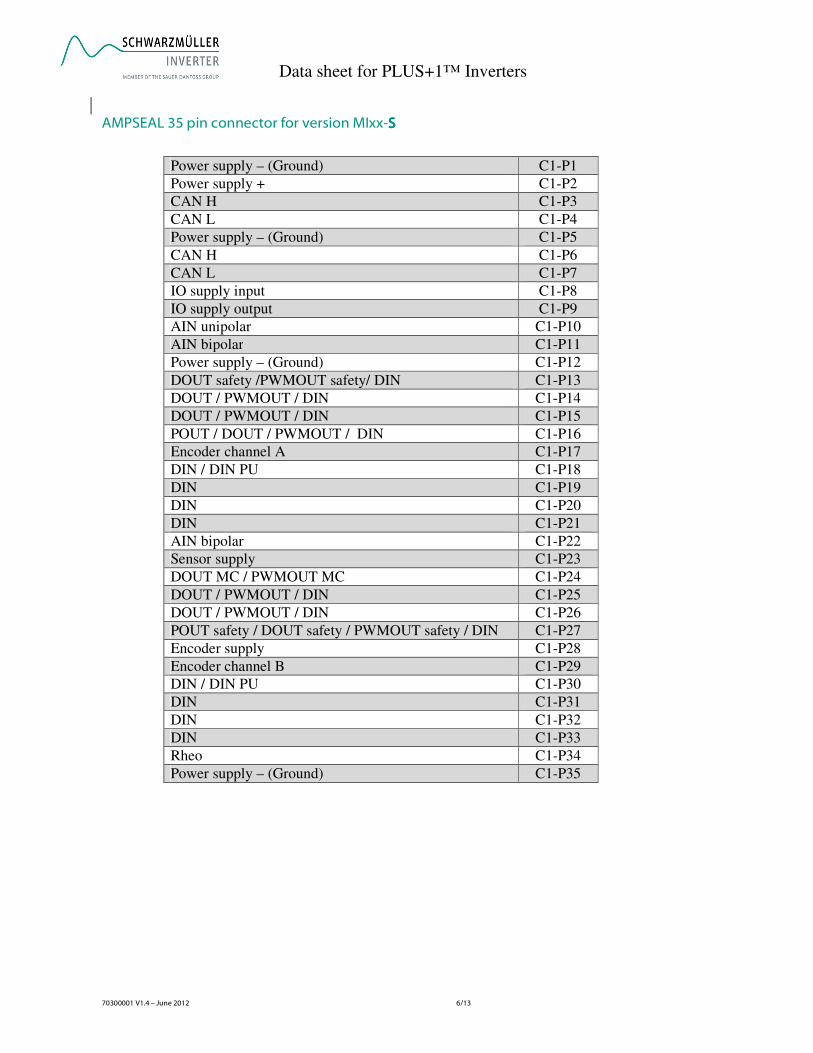
AMPSEAL 35 pin connector for version MIxx-SSSS
Power supply – (Ground) C1-P1
Power supply + C1-P2
CAN H C1-P3
CAN L C1-P4
Power supply – (Ground) C1-P5
CAN H C1-P6
CAN L C1-P7
IO supply input C1-P8
IO supply output C1-P9
AIN unipolar C1-P10
AIN bipolar C1-P11
Power supply – (Ground) C1-P12
DOUT safety /PWMOUT safety/ DIN C1-P13
DOUT / PWMOUT / DIN C1-P14
DOUT / PWMOUT / DIN C1-P15
POUT / DOUT / PWMOUT / DIN C1-P16
Encoder channel A C1-P17
DIN / DIN PU C1-P18
DIN C1-P19
DIN C1-P20
DIN C1-P21
AIN bipolar C1-P22
Sensor supply C1-P23
DOUT MC / PWMOUT MC C1-P24
DOUT / PWMOUT / DIN C1-P25
DOUT / PWMOUT / DIN C1-P26
POUT safety / DOUT safety / PWMOUT safety / DIN C1-P27
Encoder supply C1-P28
Encoder channel B C1-P29
DIN / DIN PU C1-P30
DIN C1-P31
DIN C1-P32
DIN C1-P33
Rheo C1-P34
Power supply – (Ground) C1-P35
Data sheet for PLUS+1™ Inverters
70300001 V1.4 – June 2012 7/13
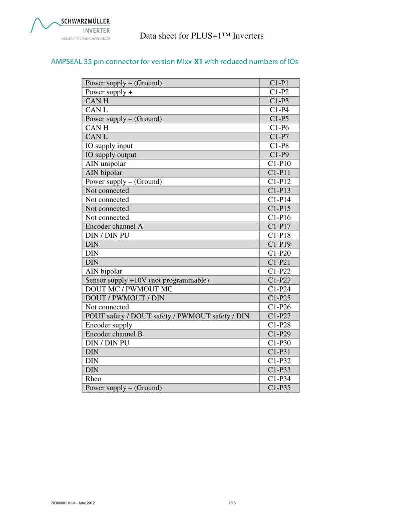
AMPSEAL 35 pin connector for version MIxx-X1X1X1X1 with reduced numbers of IOs
Power supply – (Ground) C1-P1
Power supply + C1-P2
CAN H C1-P3
CAN L C1-P4
Power supply – (Ground) C1-P5
CAN H C1-P6
CAN L C1-P7
IO supply input C1-P8
IO supply output C1-P9
AIN unipolar C1-P10
AIN bipolar C1-P11
Power supply – (Ground) C1-P12
Not connected C1-P13
Not connected C1-P14
Not connected C1-P15
Not connected C1-P16
Encoder channel A C1-P17
DIN / DIN PU C1-P18
DIN C1-P19
DIN C1-P20
DIN C1-P21
AIN bipolar C1-P22
Sensor supply +10V (not programmable) C1-P23
DOUT MC / PWMOUT MC C1-P24
DOUT / PWMOUT / DIN C1-P25
Not connected C1-P26
POUT safety / DOUT safety / PWMOUT safety / DIN C1-P27
Encoder supply C1-P28
Encoder channel B C1-P29
DIN / DIN PU C1-P30
DIN C1-P31
DIN C1-P32
DIN C1-P33
Rheo C1-P34
Power supply – (Ground) C1-P35
Data sheet for PLUS+1™ Inverters
70300001 V1.4 – June 2012 8/13
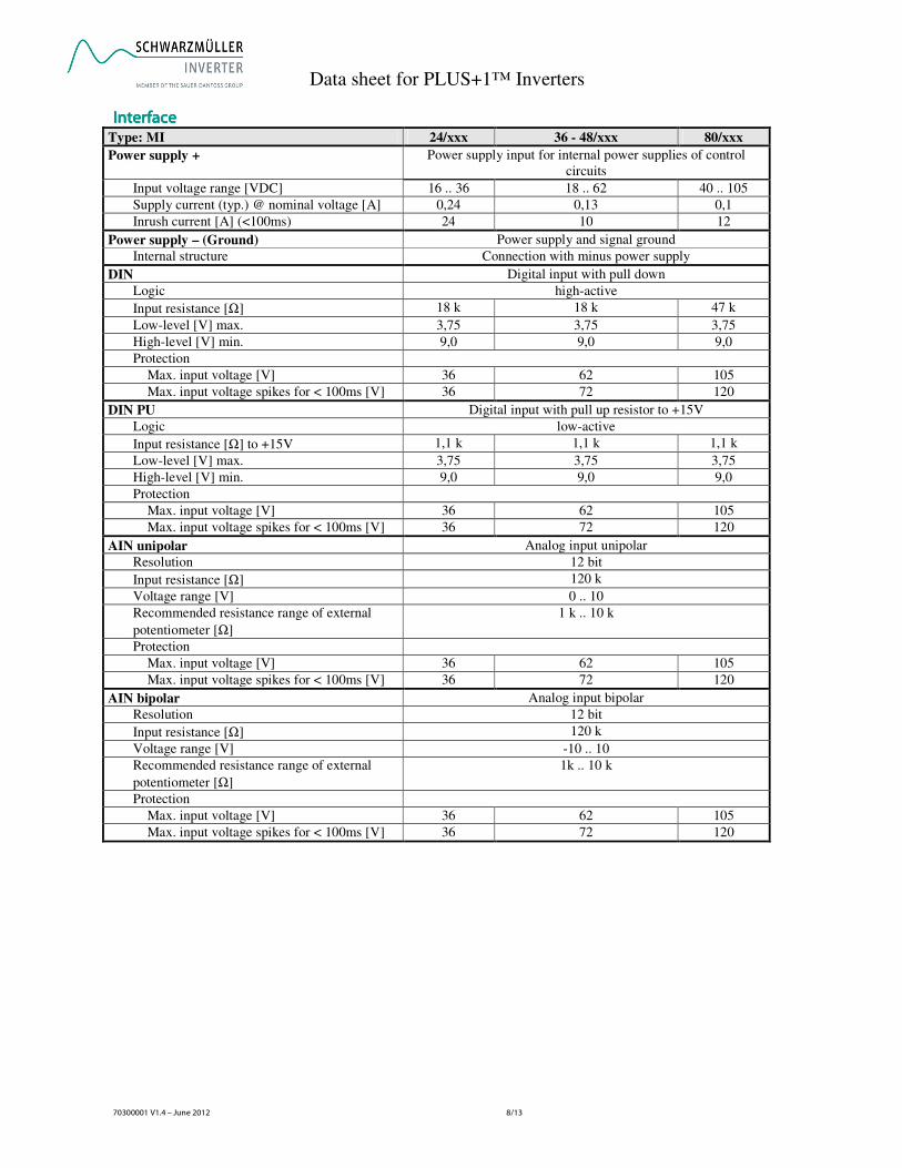
InterfaceInterfaceInterfaceInterface Type: MI 24/xxx 36 - 48/xxx 80/xxx
Power supply + Power supply input for internal power supplies of control
circuits
Input voltage range [VDC] 16 .. 36 18 .. 62 40 .. 105
Supply current (typ.) @ nominal voltage [A] 0,24 0,13 0,1
Inrush current [A] (<100ms) 24 10 12
Power supply – (Ground) Power supply and signal ground
Internal structure Connection with minus power supply
DIN Digital input with pull down
Logic high-active
Input resistance [Ω] 18 k 18 k 47 k
Low-level [V] max. 3,75 3,75 3,75
High-level [V] min. 9,0 9,0 9,0
Protection
Max. input voltage [V] 36 62 105
Max. input voltage spikes for < 100ms [V] 36 72 120
DIN PU Digital input with pull up resistor to +15V
Logic low-active
Input resistance [Ω] to +15V 1,1 k 1,1 k 1,1 k
Low-level [V] max. 3,75 3,75 3,75
High-level [V] min. 9,0 9,0 9,0
Protection
Max. input voltage [V] 36 62 105
Max. input voltage spikes for < 100ms [V] 36 72 120
AIN unipolar Analog input unipolar
Resolution 12 bit
Input resistance [Ω] 120 k
Voltage range [V] 0 .. 10
Recommended resistance range of external
potentiometer [Ω]
1 k .. 10 k
Protection
Max. input voltage [V] 36 62 105
Max. input voltage spikes for < 100ms [V] 36 72 120
AIN bipolar Analog input bipolar
Resolution 12 bit
Input resistance [Ω] 120 k
Voltage range [V] -10 .. 10
Recommended resistance range of external
potentiometer [Ω]
1k .. 10 k
Protection
Max. input voltage [V] 36 62 105
Max. input voltage spikes for < 100ms [V] 36 72 120
Data sheet for PLUS+1™ Inverters
70300001 V1.4 – June 2012 9/13
InterfaceInterfaceInterfaceInterface
Type: MI 24/xxx 36 - 48/xxx 80/xxx
IO supply input Power supply input for IOs
Maximum current [ADC] 8,0
Voltage range
Max. input voltage [V] 36 62 105
Min. input voltage [VDC] 12
IO supply output Power supply output for IOs
Maximum current [ADC] 8,0
Output voltage IO supply input
DOUT Digital output
Internal structure low-side-switch with free wheeling diode
Cathode of free wheeling diode connected to IO supply output
Signal condition Reactions time minimum 1ms,
dependent of application SW loop time.
Nominal current [A] 2,0
Maximum current [A] 6)
3,0
Resistance to minus power supply [Ohm] 136 k
Maximum load resistance [Ohm] (A higher resistance works, but will be detected as “Output
disconnected”)
45 k 266 k 468 k
PWMOUT Digital output
Internal structure low-side-switch with free wheeling diode
Cathode of free wheeling diode connected to IO supply output
Signal condition Programmable PWM signal from 0% to 100% with 10% step.
PWM frequency = 100Hz.
Nominal current [A] 2,0
Maximum current [A] 6) 3,0
Resistance to minus power supply [Ohm] 136 k
Maximum load resistance [Ohm] (A higher resistance works, but will be detected as “Output
disconnected”)
45 k 266 k 468 k
DOUT MC Digital output for main contactor
Internal structure low-side-switch with free wheeling diode
Cathode of free wheeling diode connected to Power supply +
Signal condition Reactions time minimum 1ms,
dependent of application SW loop time.
Nominal current [A] 2,0
Maximum current [A] 6)
3,0
Resistance to minus power supply [Ohm] 136 k
Maximum load resistance [Ohm] (A higher resistance works, but will be detected as “Output
disconnected”)
45 k 266 k 468 k
PWMOUT MC Digital output
Internal structure low-side-switch with free wheeling diode
Cathode of free wheeling diode connected to Power supply +
Signal condition Programmable PWM signal from 0% to 100% with 10% step.
PWM frequency = 100Hz.
Nominal current [A] 2,0
Maximum current [A] 6) 3,0
Resistance to minus power supply [Ohm] 136 k
Maximum load resistance [Ohm] (A higher resistance works, but will be detected as “Output
disconnected”)
45 k 266 k 468 k
Data sheet for PLUS+1™ Inverters
70300001 V1.4 – June 2012 10/13
InterfaceInterfaceInterfaceInterface
Type: MI 24/xxx 36 - 48/xxx 80/xxx
POUT current controlled output - superposed with dither signal
Internal structure low-side-switch with free wheeling diode
Cathode of free wheeling diode connected to IO supply output
Current range [A] 0,04…2,0
Dither signal frequency / amplitude 62,5 Hz / 0…0,25 A
Repeat accuracy from unit to unit < ±10mA (for set values 0 to 330 mA)
< ±3% (for set values 330 mA to 2A)
Switching frequency [Hz] 500 … 2000
Resistance to minus power supply [Ohm] 136 k
Maximum load resistance [Ohm] (A higher resistance works, but will be detected as “Output
disconnected”)
45 k 266 k 468 k
DOUT safety Digital output for safety relevant components
e.g. magnetic brake
Internal structure low-side-switch with additional safety switch in series
and free wheeling diode
Cathode of free wheeling diode connected to IO supply output
Signal condition Reaction time minimum 1ms,
dependent of application SW loop time
Nominal current [A] 2,0
Maximum current [A] 6)
3,0
Resistance to minus power supply [Ohm] 136 k
Maximum load resistance [Ohm] (A higher resistance works, but will be detected as “Output disconnected”)
45 k 266 k 468 k
POUT safety current controlled output for safety relevant components
e.g. lower valve - superposed with dither signal
Internal structure low-side-switch with additional safety switch in series
and free wheeling diode
Cathode of free wheeling diode connected to IO supply output
Current range [A] 0…2,0
Dither signal frequency / amplitude 62,5 Hz / 0…0,25 A
Repeat accuracy < ±10mA (for set values 0 to 330 mA)
< ±3% (for set values 330 mA to 2A)
Switching frequency [Hz] 500 … 2000
Resistance to minus power supply [Ohm] 136 k
Maximum load resistance [Ohm] (A higher resistance works, but will be detected as “Output disconnected”)
45 k 266 k 468 k
PWMOUT safety Digital output
Internal structure low-side-switch with free wheeling diode
Cathode of free wheeling diode connected to IO supply output
Signal condition Programmable PWM signal from 0% to 100% with 10% step.
PWM frequency = 100Hz.
Nominal current [A] 2,0
Maximum current [A] 6) 3,0
Resistance to minus power supply [Ohm] 136 k
Maximum load resistance [Ohm] (A higher resistance works, but will be detected as “Output
disconnected”)
45 k 266 k 468 k
Data sheet for PLUS+1™ Inverters
70300001 V1.4 – June 2012 11/13
InterfaceInterfaceInterfaceInterface
Type: MI 24/xxx 36 - 48/xxx 80/xxx
Encoder supply Power supply for encoder (e.g. sensor bearing)
Supply voltage [VDC] 13V ± 10%, Ri = 30 Ohm
Protection
Max. input voltage [V] 36 62 105
Max. input voltage spikes for < 100ms [V] 36 72 120
Over current, short circuit Current limitation at 0,1 A
Encoder channel A / Encoder channel B Square wave signal from encoder with 90° phase shift
between channel A and channel B
Internal structure Internal pull-up-resistors to power supply encoder
Pull-up-resistor [Ω] 1,1 k
Maximum frequency [kHz] (open collector) 10
Maximum frequency [kHz] (push-pull) 50
Low-level (maximum) [V] 1,77
High-level (minimum) [V] 7,1
Protection
Max. input voltage [V] 36 62 105
Max. input voltage spikes for < 100ms [V] 36 72 120
Rheo Measurement of an external resistance to minus power supply
(e.g. motor temperature sensor)
Range of resistance [Ω] 0 .. 12 k
Protection
Max. input voltage [V] 36 62 105
Max. input voltage spikes for < 100ms [V] 36 72 120
CAN H / CAN L Serial interface V2.0B
Baud rate Maximum 1 Mbps
Protection
Max. input voltage [V] 36 62 105
Max. input voltage spikes for < 100ms [V] 36 72 120
Sensor supply Power supply for external sensors
Programmable output voltage [VDC] 5 / 10 / 12 (MIxx-X1-version: Constant value = 10V)
Tolerance [%] 5
Maximum output current [A] 0,1
Protection
Max. input voltage [V] 36 62 105
Max. input voltage spikes for < 100ms [V] 36 72 120
Over current, short circuit Current limitation at 0,1 A
6)
For 1 second.
Data sheet for PLUS+1™ Inverters
70300001 V1.4 – June 2012 12/13
Wiring diagram Wiring diagram Wiring diagram Wiring diagram for version MIxxfor version MIxxfor version MIxxfor version MIxx----SSSS
120R
Thermistor
+
-
U
V
W
CAN H
CAN L
34
35
DIN / DIN PU
AIN unipolar
DOUT
DOUT
DOUT safety
DOUT MC
Power supply +
Power Supplies
21
29
18
30
19
16
27
15
26
14
25
24
17
31
10
22
DINDIN
DINDIN
DIN / DIN PU
1
2
3
4
5
6
11
23
20
DOUT
IO supply output
key
Fuse(optional)
Controller
Power Stage
32
33
13
12
7
13V
5V or 10V or 12V
CAN H
CAN L
Power ground -
+-
+-
+-
+-
B
0V
A
+13V encoder
10A
AIN bipolar
AIN bipolar
Potentiometer supply
DIN
DIN
POUT safety
28
+-
POUT
+-
I
O
I
O
I
O
I
O
I
O
I
O
I
O
DIN
DIN
DIN
DIN
DIN
DIN
DIN
+-
DOUT
Standard functions Alternative functions
B
0V
A
+13V encoder
Connector Type:AMP SEAL
Power ground -
-10V ... 0V ... +10V
parallel to first sensor bearing
(defined by parameters)
DIN PU suitable for encoder inputs
-10V ... 0V ... +10V
0V ... +10V
O
O
13
25
14
26
15
27
16
18
30
9
8 IO supply input
IO supply outputO
O
DOUT safety
DOUT
DC
DCoptional converter
emergencystop
Data sheet for PLUS+1™ Inverters
70300001 V1.4 – June 2012 13/13
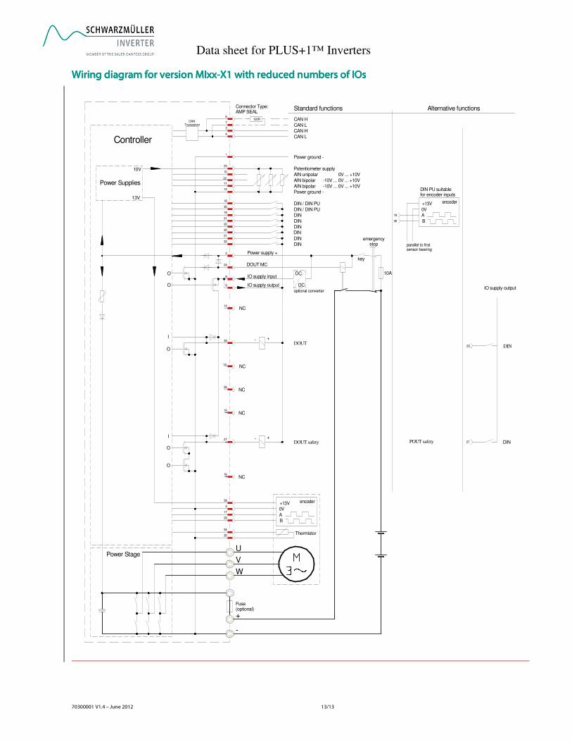
Wiring diagram for version Wiring diagram for version Wiring diagram for version Wiring diagram for version MIxxMIxxMIxxMIxx----X1 X1 X1 X1 with reduced numbers of IOswith reduced numbers of IOswith reduced numbers of IOswith reduced numbers of IOs
120R
Thermistor
+
-
U
V
W
CAN H
CAN L
34
35
DIN / DIN PU
AIN unipolar
DOUT MC
Power supply +
Power Supplies
21
29
18
30
19
16
27
15
26
14
25
24
17
31
10
DINDIN
DIN
DIN
DIN / DIN PU
1
2
3
4
5
6
11
23
20
IO supply output
key
Fuse(optional)
Controller
Power Stage
32
33
13
12
7
13V
10V
CAN H
CAN L
Power ground -
B
0V
A
+13V encoder
10A
AIN bipolar
Potentiometer supply
DIN
DIN
28
DOUT safety
+-
I
I
ODIN
Standard functions Alternative functions
B
0VA
+13V encoder
Connector Type:AMP SEAL
Power ground -
-10V ... 0V ... +10V
parallel to first sensor bearing
DIN PU suitable for encoder inputs
0V ... +10V
O
27
18
30
9
8 IO supply input
IO supply outputO
O
DIN
DC
DCoptional converter
emergencystop
POUT safety
O
DOUT25
+-
NC
NC
NC
NC
NC
22
AIN bipolar -10V ... 0V ... +10V
CAN Transceiver
Recommended