Preliminary Information
AMD-K6™-2E+Embedded Processor
Data Sheet
Publication # 23542 Rev: A Amendment/0Issue Date: September 2000
Trademarks
AMD, the AMD logo, K6, 3DNow!, and combinations thereof, AMD PowerNow!, E86, and Super7 are trademarks,FusionE86 is a service mark, and AMD-K6 and RISC86 are registered trademarks of Advanced Micro Devices,Inc.
Microsoft, Windows, and Windows NT are registered trademarks of Microsoft Corporation.
NetWare is a registered trademark of Novell, Inc.
MMX is a trademark of Intel Corporation.
Other product names used in this publication are for identification purposes only and may be trademarks oftheir respective companies.
The TAP State Diagram is reprinted from IEEE Std 1149.1-1990 “IEEE Standard Test Access Port andBoundary-Scan Architecture,” Copyright © 1990 by the Institute of Electrical and Electronics Engineers, Inc.The IEEE disclaims any responsibility or liability resulting from the placement and use in the described manner.Information is reprinted with the permission of the IEEE.
© 2000 Advanced Micro Devices, Inc. All rights reserved.
The contents of this document are provided in connection with Advanced MicroDevices, Inc. (“AMD”) products. AMD makes no representations or warranties withrespect to the accuracy or completeness of the contents of this publication andreserves the right to make changes to specifications and product descriptions at anytime without notice. No license, whether express, implied, arising by estoppel orotherwise, to any intellectual property rights is granted by this publication. Exceptas set forth in AMD's Standard Terms and Conditions of Sale, AMD assumes noliability whatsoever, and disclaims any express or implied warranty, relating to itsproducts including, but not limited to, the implied warranty of merchantability,fitness for a particular purpose, or infringement of any intellectual property right.
AMD's products are not designed, intended, authorized or warranted for use ascomponents in systems intended for surgical implant into the body, or in otherapplications intended to support or sustain life, or in any other application in whichthe failure of AMD's product could create a situation where personal injury, death,or severe property or environmental damage may occur. AMD reserves the right todiscontinue or make changes to its products at any time without notice.

23542A/0—September 2000 AMD-K6™-2E+ Embedded Processor Data Sheet
Preliminary Information
IF YOU HAVE QUESTIONS, WE’RE HERE TO HELP YOU.
The AMD customer service network includes U.S. offices, international offices, and acustomer training center. Expert technical assistance is available from the AMDworldwide staff of field application engineers and factory support staff to answerE86™ family hardware and software development questions.
Frequently accessed numbers are listed below. Additional contact information islisted on the back of this manual. AMD’s WWW site lists the latest phone numbers.
Technical Support
Answers to technical questions are available online, through e-mail, and by telephone.
Go to AMD’s home page at www.amd.com and follow the Support link for the latestAMD technical support phone numbers, software, and Frequently Asked Questions.
For technical support questions on all E86 embedded products, send e-mail [email protected] (in the US and Canada) or [email protected] (in Europe and the UK).
You can also call the AMD Corporate Applications Hotline at:
(800) 222-9323 Toll-free for U.S. and Canada
44-(0) 1276-803-299 U.K. and Europe hotline
WWW Support
For specific information on E86 products, access the AMD home page atwww.amd.com and follow the Embedded Processors link. These pages provideinformation on upcoming product releases, overviews of existing products,information on product support and tools, and a list of technical documentation.Support tools include online benchmarking tools and CodeKit software—testedsource code example applications. Many of the technical documents are availableonline in PDF form.
Questions, requests, and input concerning AMD’s WWW pages can be sent via e-mailto [email protected].
Documentation and Literature Support
Data books, user’s manuals, data sheets, application notes, and product CDs are freewith a simple phone call. Internationally, contact your local AMD sales office forproduct literature.
iii
AMD-K6™-2E+ Embedded Processor Data Sheet 23542A/0—September 2000
Preliminary Information
To order literature:
Web: www.amd.com/support/literature.html
U.S. and Canada: (800) 222-9323
Third-Party Support
AMD FusionE86SM program partners provide an array of products designed to meetcritical time-to-market needs. Products and solutions available include chipsets, emulators,hardware and software debuggers, board-level products, and software development tools,among others. The WWW site and the E86™ Family Products Development Tools CD,order #21058, describe these solutions. In addition, mature development tools andapplications for the x86 platform are widely available in the general marketplace.
iv
23542A/0—September 2000 AMD-K6™-2E+ Embedded Processor Data Sheet
Preliminary Information
Contents
Revision History . . . . . . . . . . . . . . . . . . . . . . . . . . . . . . . . . . . . . . . . . xvii
About this Data Sheet. . . . . . . . . . . . . . . . . . . . . . . . . . . . . . . . . . . . . . xix
1 AMD-K6™-2E+ Embedded Processor ........................................ 11.1 AMD-K6™-2E+ Embedded Processor Features . . . . . . . . . . . 31.2 Process Technology . . . . . . . . . . . . . . . . . . . . . . . . . . . . . . . . . . 71.3 Super7™ Platform . . . . . . . . . . . . . . . . . . . . . . . . . . . . . . . . . . . 8
2 Internal Architecture ................................................................ 112.1 Microarchitecture Overview . . . . . . . . . . . . . . . . . . . . . . . . . . 112.2 Cache, Instruction Prefetch, and Predecode Bits . . . . . . . . . 162.3 Instruction Fetch and Decode . . . . . . . . . . . . . . . . . . . . . . . . . 172.4 Centralized Scheduler . . . . . . . . . . . . . . . . . . . . . . . . . . . . . . . 212.5 Execution Units . . . . . . . . . . . . . . . . . . . . . . . . . . . . . . . . . . . . 222.6 Branch-Prediction Logic . . . . . . . . . . . . . . . . . . . . . . . . . . . . . 25
3 Software Environment ............................................................... 273.1 Registers . . . . . . . . . . . . . . . . . . . . . . . . . . . . . . . . . . . . . . . . . . 273.2 Model-Specific Registers (MSR) . . . . . . . . . . . . . . . . . . . . . . . 443.3 Memory Management Registers . . . . . . . . . . . . . . . . . . . . . . . 543.4 Paging . . . . . . . . . . . . . . . . . . . . . . . . . . . . . . . . . . . . . . . . . . . . 563.5 Descriptors and Gates . . . . . . . . . . . . . . . . . . . . . . . . . . . . . . . 593.6 Exceptions and Interrupts . . . . . . . . . . . . . . . . . . . . . . . . . . . . 623.7 Instructions Supported by the AMD-K6™-2E+ Processor . . 63
4 Logic Symbol Diagram ............................................................... 91
5 Signal Descriptions .................................................................... 935.1 Signal Terminology . . . . . . . . . . . . . . . . . . . . . . . . . . . . . . . . . 935.2 A20M# (Address Bit 20 Mask) . . . . . . . . . . . . . . . . . . . . . . . . . 945.3 A[31:3] (Address Bus) . . . . . . . . . . . . . . . . . . . . . . . . . . . . . . . 955.4 ADS# (Address Strobe) . . . . . . . . . . . . . . . . . . . . . . . . . . . . . . 965.5 ADSC# (Address Strobe Copy) . . . . . . . . . . . . . . . . . . . . . . . . 965.6 AHOLD (Address Hold) . . . . . . . . . . . . . . . . . . . . . . . . . . . . . . 975.7 AP (Address Parity) . . . . . . . . . . . . . . . . . . . . . . . . . . . . . . . . . 985.8 APCHK# (Address Parity Check) . . . . . . . . . . . . . . . . . . . . . . 995.9 BE[7:0]# (Byte Enables) . . . . . . . . . . . . . . . . . . . . . . . . . . . . . 1005.10 BF[2:0] (Bus Frequency) . . . . . . . . . . . . . . . . . . . . . . . . . . . . 1015.11 BOFF# (Backoff) . . . . . . . . . . . . . . . . . . . . . . . . . . . . . . . . . . . 1025.12 BRDY# (Burst Ready) . . . . . . . . . . . . . . . . . . . . . . . . . . . . . . 1035.13 BRDYC# (Burst Ready Copy) . . . . . . . . . . . . . . . . . . . . . . . . 1045.14 BREQ (Bus Request) . . . . . . . . . . . . . . . . . . . . . . . . . . . . . . . 1045.15 CACHE# (Cacheable Access) . . . . . . . . . . . . . . . . . . . . . . . . 1055.16 CLK (Clock) . . . . . . . . . . . . . . . . . . . . . . . . . . . . . . . . . . . . . . 1055.17 D/C# (Data/Code) . . . . . . . . . . . . . . . . . . . . . . . . . . . . . . . . . . 1065.18 D[63:0] (Data Bus) . . . . . . . . . . . . . . . . . . . . . . . . . . . . . . . . . 107
Contents v
AMD-K6™-2E+ Embedded Processor Data Sheet 23542A/0—September 2000
Preliminary Information
5.19 DP[7:0] (Data Parity) . . . . . . . . . . . . . . . . . . . . . . . . . . . . . . . 1085.20 EADS# (External Address Strobe) . . . . . . . . . . . . . . . . . . . . 1095.21 EWBE# (External Write Buffer Empty) . . . . . . . . . . . . . . . . 1105.22 FERR# (Floating-Point Error) . . . . . . . . . . . . . . . . . . . . . . . 1115.23 FLUSH# (Cache Flush) . . . . . . . . . . . . . . . . . . . . . . . . . . . . . 1125.24 HIT# (Inquire Cycle Hit) . . . . . . . . . . . . . . . . . . . . . . . . . . . . 1135.25 HITM# (Inquire Cycle Hit To Modified Line) . . . . . . . . . . . 1135.26 HLDA (Hold Acknowledge) . . . . . . . . . . . . . . . . . . . . . . . . . 1145.27 HOLD (Bus Hold Request) . . . . . . . . . . . . . . . . . . . . . . . . . . 1155.28 IGNNE# (Ignore Numeric Exception) . . . . . . . . . . . . . . . . . 1165.29 INIT (Initialization) . . . . . . . . . . . . . . . . . . . . . . . . . . . . . . . . 1175.30 INTR (Maskable Interrupt) . . . . . . . . . . . . . . . . . . . . . . . . . . 1185.31 INV (Invalidation Request) . . . . . . . . . . . . . . . . . . . . . . . . . . 1185.32 KEN# (Cache Enable) . . . . . . . . . . . . . . . . . . . . . . . . . . . . . . 1195.33 LOCK# (Bus Lock) . . . . . . . . . . . . . . . . . . . . . . . . . . . . . . . . . 1205.34 M/IO# (Memory or I/O) . . . . . . . . . . . . . . . . . . . . . . . . . . . . . 1215.35 NA# (Next Address) . . . . . . . . . . . . . . . . . . . . . . . . . . . . . . . . 1225.36 NMI (Non-Maskable Interrupt) . . . . . . . . . . . . . . . . . . . . . . . 1235.37 PCD (Page Cache Disable) . . . . . . . . . . . . . . . . . . . . . . . . . . 1245.38 PCHK# (Parity Check) . . . . . . . . . . . . . . . . . . . . . . . . . . . . . . 1255.39 PWT (Page Writethrough) . . . . . . . . . . . . . . . . . . . . . . . . . . . 1265.40 RESET (Reset) . . . . . . . . . . . . . . . . . . . . . . . . . . . . . . . . . . . . 1275.41 RSVD (Reserved) . . . . . . . . . . . . . . . . . . . . . . . . . . . . . . . . . . 1285.42 SCYC (Split Cycle) . . . . . . . . . . . . . . . . . . . . . . . . . . . . . . . . . 1295.43 SMI# (System Management Interrupt) . . . . . . . . . . . . . . . . 1305.44 SMIACT# (System Management Interrupt Active) . . . . . . 1315.45 STPCLK# (Stop Clock) . . . . . . . . . . . . . . . . . . . . . . . . . . . . . . 1325.46 TCK (Test Clock) . . . . . . . . . . . . . . . . . . . . . . . . . . . . . . . . . . 1335.47 TDI (Test Data Input) . . . . . . . . . . . . . . . . . . . . . . . . . . . . . . 1335.48 TDO (Test Data Output) . . . . . . . . . . . . . . . . . . . . . . . . . . . . 1335.49 TMS (Test Mode Select) . . . . . . . . . . . . . . . . . . . . . . . . . . . . 1345.50 TRST# (Test Reset) . . . . . . . . . . . . . . . . . . . . . . . . . . . . . . . . 1345.51 VCC2DET (VCC2 Detect) . . . . . . . . . . . . . . . . . . . . . . . . . . . 1355.52 VCC2H/L# (VCC2 High/Low) . . . . . . . . . . . . . . . . . . . . . . . . 1365.53 VID[4:0] (Voltage Identification) . . . . . . . . . . . . . . . . . . . . . 1375.54 W/R# (Write/Read) . . . . . . . . . . . . . . . . . . . . . . . . . . . . . . . . . 1385.55 WB/WT# (Writeback or Writethrough) . . . . . . . . . . . . . . . . 1395.56 Pin Tables by Type . . . . . . . . . . . . . . . . . . . . . . . . . . . . . . . . . 1405.57 Bus Cycle Definitions . . . . . . . . . . . . . . . . . . . . . . . . . . . . . . . 142
6 AMD PowerNow!™ Technology ............................................. 1436.1 Enhanced Power Management Features . . . . . . . . . . . . . . . 1436.2 Dynamic Core Frequency and Core Voltage Control . . . . . 150
7 Bus Cycles ................................................................................. 1537.1 Timing Diagrams . . . . . . . . . . . . . . . . . . . . . . . . . . . . . . . . . . 1537.2 Bus States . . . . . . . . . . . . . . . . . . . . . . . . . . . . . . . . . . . . . . . . 1557.3 Memory Reads and Writes . . . . . . . . . . . . . . . . . . . . . . . . . . 1587.4 I/O Read and Write . . . . . . . . . . . . . . . . . . . . . . . . . . . . . . . . 166
vi Contents
23542A/0—September 2000 AMD-K6™-2E+ Embedded Processor Data Sheet
Preliminary Information
7.5 Inquire and Bus Arbitration Cycles . . . . . . . . . . . . . . . . . . . 1687.6 Special Bus Cycles . . . . . . . . . . . . . . . . . . . . . . . . . . . . . . . . . 190
8 Power-on Configuration and Initialization ............................ 1998.1 Signals Sampled During the Falling Transition of
RESET . . . . . . . . . . . . . . . . . . . . . . . . . . . . . . . . . . . . . . . . . . . 1998.2 RESET Requirements . . . . . . . . . . . . . . . . . . . . . . . . . . . . . . 2008.3 State of Processor After RESET . . . . . . . . . . . . . . . . . . . . . . 2008.4 State of Processor After INIT . . . . . . . . . . . . . . . . . . . . . . . . 203
9 Cache Organization .................................................................. 2059.1 MESI States in the L1 Data Cache and L2 Cache . . . . . . . . 2079.2 Predecode Bits . . . . . . . . . . . . . . . . . . . . . . . . . . . . . . . . . . . . 2089.3 Cache Operation . . . . . . . . . . . . . . . . . . . . . . . . . . . . . . . . . . . 2089.4 Cache Disabling and Flushing . . . . . . . . . . . . . . . . . . . . . . . 2119.5 L2 Cache Testing . . . . . . . . . . . . . . . . . . . . . . . . . . . . . . . . . . 2139.6 Cache-Line Fills . . . . . . . . . . . . . . . . . . . . . . . . . . . . . . . . . . . 2139.7 Cache-Line Replacements . . . . . . . . . . . . . . . . . . . . . . . . . . . 2149.8 Write Allocate . . . . . . . . . . . . . . . . . . . . . . . . . . . . . . . . . . . . . 2159.9 Prefetching . . . . . . . . . . . . . . . . . . . . . . . . . . . . . . . . . . . . . . . 2209.10 Cache States . . . . . . . . . . . . . . . . . . . . . . . . . . . . . . . . . . . . . . 2219.11 Cache Coherency . . . . . . . . . . . . . . . . . . . . . . . . . . . . . . . . . . 2229.12 Writethrough and Writeback Coherency States . . . . . . . . . 2279.13 A20M# Masking of Cache Accesses . . . . . . . . . . . . . . . . . . . 227
10 Write Merge Buffer ................................................................. 22910.1 EWBE# Control . . . . . . . . . . . . . . . . . . . . . . . . . . . . . . . . . . . . 22910.2 Memory Type Range Registers . . . . . . . . . . . . . . . . . . . . . . . 23110.3 Memory-Range Restrictions . . . . . . . . . . . . . . . . . . . . . . . . . 23310.4 Examples . . . . . . . . . . . . . . . . . . . . . . . . . . . . . . . . . . . . . . . . . 235
11 Floating-Point and Multimedia Execution Units .................. 23711.1 Floating-Point Execution Unit . . . . . . . . . . . . . . . . . . . . . . . 23711.2 Multimedia and 3DNow!™ Execution Units . . . . . . . . . . . . 23911.3 Floating-Point and MMX™/3DNow!™ Instruction
Compatibility . . . . . . . . . . . . . . . . . . . . . . . . . . . . . . . . . . . . . 240
12 System Management Mode (SMM) ........................................ 24112.1 SMM Operating Mode and Default Register Values . . . . . 24112.2 SMM State-Save Area . . . . . . . . . . . . . . . . . . . . . . . . . . . . . . 24312.3 SMM Revision Identifier . . . . . . . . . . . . . . . . . . . . . . . . . . . . 24512.4 SMM Base Address . . . . . . . . . . . . . . . . . . . . . . . . . . . . . . . . . 24612.5 Halt Restart Slot . . . . . . . . . . . . . . . . . . . . . . . . . . . . . . . . . . . 24612.6 I/O Trap Doubleword . . . . . . . . . . . . . . . . . . . . . . . . . . . . . . . 24712.7 I/O Trap Restart Slot . . . . . . . . . . . . . . . . . . . . . . . . . . . . . . . 24812.8 Exceptions, Interrupts, and Debug in SMM . . . . . . . . . . . . 250
13 Test and Debug ......................................................................... 25113.1 Built-In Self-Test (BIST) . . . . . . . . . . . . . . . . . . . . . . . . . . . . 25113.2 Three-State Test Mode . . . . . . . . . . . . . . . . . . . . . . . . . . . . . . 25213.3 Boundary-Scan Test Access Port (TAP) . . . . . . . . . . . . . . . . 253
Contents vii
AMD-K6™-2E+ Embedded Processor Data Sheet 23542A/0—September 2000
Preliminary Information
13.4 Cache Inhibit . . . . . . . . . . . . . . . . . . . . . . . . . . . . . . . . . . . . . 26313.5 L2 Cache and Tag Array Testing . . . . . . . . . . . . . . . . . . . . . 26413.6 Debug . . . . . . . . . . . . . . . . . . . . . . . . . . . . . . . . . . . . . . . . . . . . 268
14 Clock Control ............................................................................ 27514.1 Clock Control States . . . . . . . . . . . . . . . . . . . . . . . . . . . . . . . 27514.2 Halt State . . . . . . . . . . . . . . . . . . . . . . . . . . . . . . . . . . . . . . . . 27814.3 Stop Grant State . . . . . . . . . . . . . . . . . . . . . . . . . . . . . . . . . . . 27814.4 Stop Grant Inquire State . . . . . . . . . . . . . . . . . . . . . . . . . . . . 28014.5 EPM Stop Grant State . . . . . . . . . . . . . . . . . . . . . . . . . . . . . . 28114.6 Stop Clock State . . . . . . . . . . . . . . . . . . . . . . . . . . . . . . . . . . . 283
15 Electrical Data .......................................................................... 28515.1 Operating Ranges . . . . . . . . . . . . . . . . . . . . . . . . . . . . . . . . . . 28615.2 Absolute Ratings . . . . . . . . . . . . . . . . . . . . . . . . . . . . . . . . . . 28715.3 DC Characteristics . . . . . . . . . . . . . . . . . . . . . . . . . . . . . . . . . 28715.4 Power Dissipation . . . . . . . . . . . . . . . . . . . . . . . . . . . . . . . . . . 28915.5 Power and Grounding . . . . . . . . . . . . . . . . . . . . . . . . . . . . . . 291
16 Signal Switching Characteristics ............................................ 29516.1 CLK Switching Characteristics . . . . . . . . . . . . . . . . . . . . . . . 29616.2 Clock Switching Characteristics for 100-MHz Bus
Operation . . . . . . . . . . . . . . . . . . . . . . . . . . . . . . . . . . . . . . . . 29616.3 Clock Switching Characteristics for 66-MHz Bus
Operation . . . . . . . . . . . . . . . . . . . . . . . . . . . . . . . . . . . . . . . . 29716.4 Valid Delay, Float, Setup, and Hold Timings . . . . . . . . . . . 29816.5 Output Delay Timings for 100-MHz Bus Operation . . . . . . 29816.6 Input Setup and Hold Timings for 100-MHz Bus
Operation . . . . . . . . . . . . . . . . . . . . . . . . . . . . . . . . . . . . . . . . 30016.7 Output Delay Timings for 66-MHz Bus Operation . . . . . . . 30216.8 Input Setup and Hold Timings for 66-MHz Bus
Operation . . . . . . . . . . . . . . . . . . . . . . . . . . . . . . . . . . . . . . . . 30416.9 RESET and Test Signal Timing . . . . . . . . . . . . . . . . . . . . . . 30616.10 Timing Diagrams . . . . . . . . . . . . . . . . . . . . . . . . . . . . . . . . . . 309
17 Thermal Design ........................................................................ 31317.1 Package Thermal Specifications . . . . . . . . . . . . . . . . . . . . . . 31317.2 Measuring Case Temperature . . . . . . . . . . . . . . . . . . . . . . . . 31717.3 Layout and Airflow Considerations . . . . . . . . . . . . . . . . . . . 317
18 Pin Designations ....................................................................... 32118.1 Pins Designations for CPGA Package . . . . . . . . . . . . . . . . . 32218.2 Pins Designations for OBGA Package . . . . . . . . . . . . . . . . . 326
19 Package Specifications ............................................................ 33119.1 321-Pin Staggered CPGA Package Specification . . . . . . . . 33119.2 349-Ball OBGA Package Specification . . . . . . . . . . . . . . . . . 332
20 Ordering Information .............................................................. 333
Index. . . . . . . . . . . . . . . . . . . . . . . . . . . . . . . . . . . . . . . . . . . . . . . . . . . 335
viii Contents
23542A/0—September 2000 AMD-K6™-2E+ Embedded Processor Data Sheet
Preliminary Information
List of Figures
Figure 1. AMD-K6™-2E+ Processor Block Diagram . . . . . . . . . . . . . . . . . 13
Figure 2. Cache Sector Organization . . . . . . . . . . . . . . . . . . . . . . . . . . . . . 16
Figure 3. The Instruction Buffer . . . . . . . . . . . . . . . . . . . . . . . . . . . . . . . . . 18
Figure 4. AMD-K6™-2E+ Processor Decode Logic . . . . . . . . . . . . . . . . . . 19
Figure 5. AMD-K6™-2E+ Processor Scheduler . . . . . . . . . . . . . . . . . . . . . 22
Figure 6. Register X and Y Pipeline Functional Units. . . . . . . . . . . . . . . 24
Figure 7. EAX Register with 16-Bit and 8-Bit Name Components. . . . . . 28
Figure 8. Integer Data Registers. . . . . . . . . . . . . . . . . . . . . . . . . . . . . . . . . 29
Figure 9. Segment Register . . . . . . . . . . . . . . . . . . . . . . . . . . . . . . . . . . . . . 30
Figure 10. Segment Usage . . . . . . . . . . . . . . . . . . . . . . . . . . . . . . . . . . . . . . . 31
Figure 11. Floating-Point Register . . . . . . . . . . . . . . . . . . . . . . . . . . . . . . . . 32
Figure 12. FPU Status Word Register . . . . . . . . . . . . . . . . . . . . . . . . . . . . . 32
Figure 13. FPU Control Word Register . . . . . . . . . . . . . . . . . . . . . . . . . . . . 33
Figure 14. FPU Tag Word Register. . . . . . . . . . . . . . . . . . . . . . . . . . . . . . . . 33
Figure 15. Packed Decimal Data Register . . . . . . . . . . . . . . . . . . . . . . . . . . 34
Figure 16. Precision Real Data Registers . . . . . . . . . . . . . . . . . . . . . . . . . . 34
Figure 17. MMX™/3DNow!™ Registers . . . . . . . . . . . . . . . . . . . . . . . . . . . . 35
Figure 18. MMX™ Technology Data Types . . . . . . . . . . . . . . . . . . . . . . . . . 36
Figure 19. 3DNow!™ Technology Data Types . . . . . . . . . . . . . . . . . . . . . . . 37
Figure 20. EFLAGS Registers . . . . . . . . . . . . . . . . . . . . . . . . . . . . . . . . . . . . 38
Figure 21. Control Register 4 (CR4) . . . . . . . . . . . . . . . . . . . . . . . . . . . . . . . 39
Figure 22. Control Register 3 (CR3) . . . . . . . . . . . . . . . . . . . . . . . . . . . . . . . 39
Figure 23. Control Register 2 (CR2) . . . . . . . . . . . . . . . . . . . . . . . . . . . . . . . 39
Figure 24. Control Register 1 (CR1) . . . . . . . . . . . . . . . . . . . . . . . . . . . . . . . 40
Figure 25. Control Register 0 (CR0) . . . . . . . . . . . . . . . . . . . . . . . . . . . . . . . 40
Figure 26. Debug Register DR7 . . . . . . . . . . . . . . . . . . . . . . . . . . . . . . . . . . 41
Figure 27. Debug Register DR6 . . . . . . . . . . . . . . . . . . . . . . . . . . . . . . . . . . 42
Figure 28. Debug Registers DR5 and DR4. . . . . . . . . . . . . . . . . . . . . . . . . . 42
Figure 29. Debug Registers DR3, DR2, DR1, and DR0. . . . . . . . . . . . . . . . 43
Figure 30. Machine-Check Address Register (MCAR) . . . . . . . . . . . . . . . . 45
Figure 31. Machine-Check Type Register (MCTR) . . . . . . . . . . . . . . . . . . . 45
Figure 32. Test Register 12 (TR12). . . . . . . . . . . . . . . . . . . . . . . . . . . . . . . . 46
Figure 33. Time Stamp Counter (TSC) . . . . . . . . . . . . . . . . . . . . . . . . . . . . . 46
Figure 34. Extended Feature Enable Register (EFER) . . . . . . . . . . . . . . . 47
Figure 35. SYSCALL/SYSRET Target Address Register (STAR) . . . . . . . 48
Figure 36. Write Handling Control Register (WHCR) . . . . . . . . . . . . . . . . 48
List of Figures ix
AMD-K6™-2E+ Embedded Processor Data Sheet 23542A/0—September 2000
Preliminary Information
Figure 37. UC/WC Cacheability Control Register (UWCCR) . . . . . . . . . . 49
Figure 38. Processor State Observability Register (PSOR) . . . . . . . . . . . . 49
Figure 39. Page Flush/Invalidate Register (PFIR) . . . . . . . . . . . . . . . . . . . 50
Figure 40. L2 Tag or Data Location for AMD-K6™-2E+
Processor—EDX . . . . . . . . . . . . . . . . . . . . . . . . . . . . . . . . . . . . . . 51
Figure 41. L2 Data —EAX . . . . . . . . . . . . . . . . . . . . . . . . . . . . . . . . . . . . . . . 51
Figure 42. L2 Tag Information for AMD-K6™-2E+ Processor—EAX . . . . 52
Figure 43. Enhanced Power Management Register (EPMR). . . . . . . . . . . 53
Figure 44. Memory Management Registers . . . . . . . . . . . . . . . . . . . . . . . . . 54
Figure 45. Task State Segment (TSS) . . . . . . . . . . . . . . . . . . . . . . . . . . . . . . 55
Figure 46. 4-Kbyte Paging Mechanism . . . . . . . . . . . . . . . . . . . . . . . . . . . . . 56
Figure 47. 4-Mbyte Paging Mechanism . . . . . . . . . . . . . . . . . . . . . . . . . . . . 57
Figure 48. Page Directory Entry 4-Kbyte Page Table (PDE) . . . . . . . . . . . 58
Figure 49. Page Directory Entry 4-Mbyte Page Table (PDE) . . . . . . . . . . 58
Figure 50. Page Table Entry (PTE). . . . . . . . . . . . . . . . . . . . . . . . . . . . . . . . 59
Figure 51. Application Segment Descriptor . . . . . . . . . . . . . . . . . . . . . . . . 60
Figure 52. System Segment Descriptor . . . . . . . . . . . . . . . . . . . . . . . . . . . . 61
Figure 53. Gate Descriptor . . . . . . . . . . . . . . . . . . . . . . . . . . . . . . . . . . . . . . 62
Figure 54. Enhanced Power Management Register (EPMR). . . . . . . . . . 144
Figure 55. EPM 16-Byte I/O Block. . . . . . . . . . . . . . . . . . . . . . . . . . . . . . . . 146
Figure 56. Bus Divisor and Voltage ID Control (BVC) Field . . . . . . . . . . 147
Figure 57. Processor State Observability Register (PSOR)—Low-
Power Versions of the Processor . . . . . . . . . . . . . . . . . . . . . . . 148
Figure 58. Waveform Definitions . . . . . . . . . . . . . . . . . . . . . . . . . . . . . . . . 154
Figure 59. Bus State Machine Diagram . . . . . . . . . . . . . . . . . . . . . . . . . . . 155
Figure 60. Non-Pipelined Single-Transfer Memory Read/Write and
Write Delayed by EWBE# . . . . . . . . . . . . . . . . . . . . . . . . . . . . . 159
Figure 61. Misaligned Single-Transfer Memory Read and Write . . . . . . 161
Figure 62. Burst Reads and Pipelined Burst Reads . . . . . . . . . . . . . . . . . 163
Figure 63. Burst Writeback due to Cache-Line Replacement . . . . . . . . . 165
Figure 64. Basic I/O Read and Write . . . . . . . . . . . . . . . . . . . . . . . . . . . . . 166
Figure 65. Misaligned I/O Transfer. . . . . . . . . . . . . . . . . . . . . . . . . . . . . . . 167
Figure 66. Basic HOLD/HLDA Operation . . . . . . . . . . . . . . . . . . . . . . . . . 169
Figure 67. HOLD-Initiated Inquire Hit to Shared or Exclusive Line . . . 171
Figure 68. HOLD-Initiated Inquire Hit to Modified Line. . . . . . . . . . . . . 173
Figure 69. AHOLD-Initiated Inquire Miss . . . . . . . . . . . . . . . . . . . . . . . . . 175
Figure 70. AHOLD-Initiated Inquire Hit to Shared or Exclusive Line . . 177
Figure 71. AHOLD-Initiated Inquire Hit to Modified Line . . . . . . . . . . . 179
Figure 72. AHOLD Restriction . . . . . . . . . . . . . . . . . . . . . . . . . . . . . . . . . . 181
x List of Figures
23542A/0—September 2000 AMD-K6™-2E+ Embedded Processor Data Sheet
Preliminary Information
Figure 73. BOFF# Timing. . . . . . . . . . . . . . . . . . . . . . . . . . . . . . . . . . . . . . . 183
Figure 74. Basic Locked Operation. . . . . . . . . . . . . . . . . . . . . . . . . . . . . . . 185
Figure 75. Locked Operation with BOFF# Intervention. . . . . . . . . . . . . . 187
Figure 76. Interrupt Acknowledge Operation . . . . . . . . . . . . . . . . . . . . . . 189
Figure 77. Basic Special Bus Cycle (Halt Cycle) . . . . . . . . . . . . . . . . . . . . 191
Figure 78. Shutdown Cycle . . . . . . . . . . . . . . . . . . . . . . . . . . . . . . . . . . . . . 192
Figure 79. Stop Grant and Stop Clock Modes, Part 1 . . . . . . . . . . . . . . . . 194
Figure 80. Stop Grant and Stop Clock Modes, Part 2 . . . . . . . . . . . . . . . . 195
Figure 81. INIT-Initiated Transition from Protected Mode to Real
Mode . . . . . . . . . . . . . . . . . . . . . . . . . . . . . . . . . . . . . . . . . . . . . . 197
Figure 82. L1 and L2 Cache Organization for the AMD-K6™-2E+
Processor . . . . . . . . . . . . . . . . . . . . . . . . . . . . . . . . . . . . . . . . . . . 206
Figure 83. L1 Cache Sector Organization. . . . . . . . . . . . . . . . . . . . . . . . . . 207
Figure 84. Write Handling Control Register (WHCR) . . . . . . . . . . . . . . . 217
Figure 85. Write Allocate Logic Mechanisms and Conditions . . . . . . . . . 218
Figure 86. Page Flush/Invalidate Register (PFIR) . . . . . . . . . . . . . . . . . . 224
Figure 87. UC/WC Cacheability Control Register (UWCCR) . . . . . . . . . 232
Figure 88. External Logic for Supporting Floating-Point Exceptions. . . 239
Figure 89. SMM Memory . . . . . . . . . . . . . . . . . . . . . . . . . . . . . . . . . . . . . . . 242
Figure 90. TAP State Diagram . . . . . . . . . . . . . . . . . . . . . . . . . . . . . . . . . . 261
Figure 91. L2 Cache Organization for AMD-K6™-2E+ Processor . . . . . . 265
Figure 92. L2 Cache Sector and Line Organization . . . . . . . . . . . . . . . . . 265
Figure 93. L2 Tag or Data Location for the AMD-K6™-2E+
Processor—EDX . . . . . . . . . . . . . . . . . . . . . . . . . . . . . . . . . . . . . 266
Figure 94. L2 Data - EAX. . . . . . . . . . . . . . . . . . . . . . . . . . . . . . . . . . . . . . . 267
Figure 95. L2 Tag Information for the AMD-K6™-2E+
Processor—EAX . . . . . . . . . . . . . . . . . . . . . . . . . . . . . . . . . . . . . 267
Figure 96. LRU Byte. . . . . . . . . . . . . . . . . . . . . . . . . . . . . . . . . . . . . . . . . . . 268
Figure 97. Debug Register DR7 . . . . . . . . . . . . . . . . . . . . . . . . . . . . . . . . . 269
Figure 98. Debug Register DR6 . . . . . . . . . . . . . . . . . . . . . . . . . . . . . . . . . 270
Figure 99. Debug Registers DR5 and DR4. . . . . . . . . . . . . . . . . . . . . . . . . 270
Figure 100. Debug Registers DR3, DR2, DR1, and DR0. . . . . . . . . . . . . . . 271
Figure 101. Clock Control State Transitions for Standard-Power
Versions of the AMD-K6™-2E+ Processor . . . . . . . . . . . . . . . . 276
Figure 102. Clock Control State Transitions for Low-Power
Versions of the AMD-K6™-2E+ Processor . . . . . . . . . . . . . . . . 277
Figure 103. Suggested Component Placement for CPGA Package . . . . . . 292
Figure 104. CLK Waveform . . . . . . . . . . . . . . . . . . . . . . . . . . . . . . . . . . . . . . 297
Figure 105. Key to Timing Diagrams . . . . . . . . . . . . . . . . . . . . . . . . . . . . . . 309
List of Figures xi
AMD-K6™-2E+ Embedded Processor Data Sheet 23542A/0—September 2000
Preliminary Information
Figure 106. Output Valid Delay Timing . . . . . . . . . . . . . . . . . . . . . . . . . . . . 310
Figure 107. Maximum Float Delay Timing . . . . . . . . . . . . . . . . . . . . . . . . . 310
Figure 108. Input Setup and Hold Timing . . . . . . . . . . . . . . . . . . . . . . . . . . 310
Figure 109. Reset and Configuration Timing . . . . . . . . . . . . . . . . . . . . . . . 311
Figure 110. TCK Waveform . . . . . . . . . . . . . . . . . . . . . . . . . . . . . . . . . . . . . . 312
Figure 111. TRST# Timing. . . . . . . . . . . . . . . . . . . . . . . . . . . . . . . . . . . . . . . 312
Figure 112. Test Signal Timing Diagram . . . . . . . . . . . . . . . . . . . . . . . . . . . 312
Figure 113. Thermal Model (CPGA Package) . . . . . . . . . . . . . . . . . . . . . . . 315
Figure 114. Power Consumption and Thermal Resistance
(CPGA Package) . . . . . . . . . . . . . . . . . . . . . . . . . . . . . . . . . . . . . 315
Figure 115. Processor Heat Dissipation Path . . . . . . . . . . . . . . . . . . . . . . . 316
Figure 116. Measuring Case Temperature. . . . . . . . . . . . . . . . . . . . . . . . . . 317
Figure 117. Voltage Regulator Placement . . . . . . . . . . . . . . . . . . . . . . . . . . 318
Figure 118. Airflow for a Heatsink with Fan . . . . . . . . . . . . . . . . . . . . . . . . 319
Figure 119. Airflow Path in a Dual-Fan System . . . . . . . . . . . . . . . . . . . . . 319
Figure 120. Airflow Path in an ATX Form-Factor System . . . . . . . . . . . . . 320
Figure 121. CPGA Connection Diagram (Top-Side View) . . . . . . . . . . . . . 322
Figure 122. CPGA Connection Diagram (Bottom-Side View) . . . . . . . . . . 323
Figure 123. OBGA Connection Diagram (Top-Side View) . . . . . . . . . . . . . 326
Figure 124. OBGA Connection Diagram (Bottom-Side View) . . . . . . . . . . 327
Figure 125. 321-Pin Staggered CPGA Package Specification . . . . . . . . . . 331
Figure 126. 349-Ball OBGA Package Specification . . . . . . . . . . . . . . . . . . . 332
xii List of Figures
23542A/0—September 2000 AMD-K6™-2E+ Embedded Processor Data Sheet
Preliminary Information
List of Tables
Table 1. Execution Latency and Throughput of Execution Units . . . . . 23Table 2. General-Purpose Registers . . . . . . . . . . . . . . . . . . . . . . . . . . . . . 28Table 3. General-Purpose Register Doubleword, Word, and Byte
Names . . . . . . . . . . . . . . . . . . . . . . . . . . . . . . . . . . . . . . . . . . . . . . 29Table 4. Segment Registers . . . . . . . . . . . . . . . . . . . . . . . . . . . . . . . . . . . . 30Table 5. AMD-K6™-2E+ Processor Model-Specific Registers . . . . . . . . 44Table 6. Extended Feature Enable Register (EFER) Definition . . . . . . 47Table 7. SYSCALL/SYSRET Target Address Register (STAR)
Definition . . . . . . . . . . . . . . . . . . . . . . . . . . . . . . . . . . . . . . . . . . . 48Table 8. Memory Management Registers . . . . . . . . . . . . . . . . . . . . . . . . . 54Table 9. Application Segment Types . . . . . . . . . . . . . . . . . . . . . . . . . . . . 60Table 10. System Segment and Gate Types . . . . . . . . . . . . . . . . . . . . . . . . 61Table 11. Summary of Exceptions and Interrupts . . . . . . . . . . . . . . . . . . . 62Table 12. Integer Instructions . . . . . . . . . . . . . . . . . . . . . . . . . . . . . . . . . . . 65Table 13. Floating-Point Instructions . . . . . . . . . . . . . . . . . . . . . . . . . . . . . 82Table 14. MMX™ Instructions . . . . . . . . . . . . . . . . . . . . . . . . . . . . . . . . . . . 86Table 15. 3DNow!™ Instructions . . . . . . . . . . . . . . . . . . . . . . . . . . . . . . . . . 89Table 16. 3DNow!™ Technology DSP Extensions . . . . . . . . . . . . . . . . . . . 90Table 17. Processor-to-Bus Clock Ratios. . . . . . . . . . . . . . . . . . . . . . . . . . 101Table 18. Output Pin Float Conditions for VCC2 High/Low. . . . . . . . . . 136Table 19. Input Pin Types . . . . . . . . . . . . . . . . . . . . . . . . . . . . . . . . . . . . . 140Table 20. Output Pin Float Conditions . . . . . . . . . . . . . . . . . . . . . . . . . . . 141Table 21. Input/Output Pin Float Conditions. . . . . . . . . . . . . . . . . . . . . . 141Table 22. Test Pin Types . . . . . . . . . . . . . . . . . . . . . . . . . . . . . . . . . . . . . . 141Table 23. Bus Cycle Definition . . . . . . . . . . . . . . . . . . . . . . . . . . . . . . . . . 142Table 24. Special Cycles . . . . . . . . . . . . . . . . . . . . . . . . . . . . . . . . . . . . . . . 142Table 25. Enhanced Power Management Register (EPMR) Definition 145Table 26. EPM 16-Byte I/O Block Definition . . . . . . . . . . . . . . . . . . . . . . 146Table 27. Bus Divisor and Voltage ID Control (BVC) Definition . . . . . . 147Table 28. Processor-to-Bus Clock Ratios. . . . . . . . . . . . . . . . . . . . . . . . . . 149Table 29. Bus-Cycle Order During Misaligned Memory Transfers . . . . 160Table 30. A[4:3] Address-Generation Sequence During Bursts . . . . . . . 162Table 31. Bus-Cycle Order During Misaligned I/O Transfers . . . . . . . . . 167Table 32. Interrupt Acknowledge Operation Definition. . . . . . . . . . . . . 188Table 33. Encodings for Special Bus Cycles . . . . . . . . . . . . . . . . . . . . . . . 190Table 34. Output Signal State After RESET . . . . . . . . . . . . . . . . . . . . . . 200Table 35. Register State After RESET . . . . . . . . . . . . . . . . . . . . . . . . . . . 201Table 36. PWT Signal Generation . . . . . . . . . . . . . . . . . . . . . . . . . . . . . . . 210Table 37. PCD Signal Generation . . . . . . . . . . . . . . . . . . . . . . . . . . . . . . . 210Table 38. CACHE# Signal Generation . . . . . . . . . . . . . . . . . . . . . . . . . . . 211Table 39. L1 and L2 Cache States for Read and Write Accesses . . . . . . 221
List of Tables xiii
AMD-K6™-2E+ Embedded Processor Data Sheet 23542A/0—September 2000
Preliminary Information
Table 40. Valid L1 and L2 Cache States and Effect of Inquire Cycles . 225Table 41. L1 and L2 Cache States for Snoops, Flushes, and
Invalidation. . . . . . . . . . . . . . . . . . . . . . . . . . . . . . . . . . . . . . . . . 226Table 42. EWBEC Settings and Performance . . . . . . . . . . . . . . . . . . . . . 231Table 43. WC/UC Memory Type . . . . . . . . . . . . . . . . . . . . . . . . . . . . . . . . 233Table 44. Valid Masks and Range Sizes for UWCCR Register . . . . . . . 234Table 45. Initial State of Registers in SMM . . . . . . . . . . . . . . . . . . . . . . . 243Table 46. SMM State-Save Area Map . . . . . . . . . . . . . . . . . . . . . . . . . . . . 243Table 47. SMM Revision Identifier . . . . . . . . . . . . . . . . . . . . . . . . . . . . . . 246Table 48. I/O Trap Doubleword Configuration . . . . . . . . . . . . . . . . . . . . 248Table 49. I/O Trap Restart Slot . . . . . . . . . . . . . . . . . . . . . . . . . . . . . . . . . 249Table 50. Boundary Scan Bit Definitions . . . . . . . . . . . . . . . . . . . . . . . . . 257Table 51. Device Identification Register . . . . . . . . . . . . . . . . . . . . . . . . . 259Table 52. Supported TAP Instructions . . . . . . . . . . . . . . . . . . . . . . . . . . . 259Table 53. Tag versus Data Selector . . . . . . . . . . . . . . . . . . . . . . . . . . . . . . 266Table 54. DR7 LEN and RW Definitions . . . . . . . . . . . . . . . . . . . . . . . . . 273Table 55. Operating Ranges for Low-Power AMD-K6™-2E+ Devices . . 286Table 56. Operating Ranges for Standard-Power AMD-K6™-2E+
Devices . . . . . . . . . . . . . . . . . . . . . . . . . . . . . . . . . . . . . . . . . . . . 286Table 57. Absolute Ratings . . . . . . . . . . . . . . . . . . . . . . . . . . . . . . . . . . . . 287Table 58. DC Characteristics for the AMD-K6™-2E+ Processor . . . . . . 287Table 59. Power Dissipation for Low-Power AMD-K6™-2E+ Devices . . 289Table 60. Power Dissipation for Standard-Power AMD-K6™-2E+
Devices . . . . . . . . . . . . . . . . . . . . . . . . . . . . . . . . . . . . . . . . . . . . 290Table 61. Supported Voltages and Operating Frequencies for Low-
Power AMD-K6™-2E+ Processors Enabled with AMD PowerNow!™ Technology . . . . . . . . . . . . . . . . . . . . . . . . . . . . . 290
Table 62. CLK Switching Characteristics for 100-MHz Bus Operation . 296Table 63. CLK Switching Characteristics for 66-MHz Bus Operation . . 297Table 64. Output Delay Timings for 100-MHz Bus Operation . . . . . . . . 298Table 65. Input Setup and Hold Timings for 100-MHz Bus Operation . 300Table 66. Output Delay Timings for 66-MHz Bus Operation . . . . . . . . . 302Table 67. Input Setup and Hold Timings for 66-MHz Bus Operation . . 304Table 68. RESET and Configuration Signals for 100-MHz Bus
Operation . . . . . . . . . . . . . . . . . . . . . . . . . . . . . . . . . . . . . . . . . . 306Table 69. RESET and Configuration Signals for 66-MHz Bus
Operation . . . . . . . . . . . . . . . . . . . . . . . . . . . . . . . . . . . . . . . . . . 307Table 70. TCK Waveform and TRST# Timing at 25 MHz . . . . . . . . . . . . 308Table 71. Test Signal Timing at 25 MHz . . . . . . . . . . . . . . . . . . . . . . . . . . 308Table 72. Package Thermal Specification for Low-Power
AMD-K6™-2E+ Devices . . . . . . . . . . . . . . . . . . . . . . . . . . . . . . . 314Table 73. Package Thermal Specification for Standard-Power
AMD-K6™-2E+ Devices . . . . . . . . . . . . . . . . . . . . . . . . . . . . . . . 314Table 74. Pin Differences Between the CPGA and OBGA Packages. . . 321
xiv List of Tables

23542A/0—September 2000 AMD-K6™-2E+ Embedded Processor Data Sheet
Preliminary Information
Table 75. CPGA Pin Designations by Functional Grouping . . . . . . . . . . 324Table 76. CPGA Pin Designations for No Connect, Reserved, Power,
and Ground Pins . . . . . . . . . . . . . . . . . . . . . . . . . . . . . . . . . . . . . 325Table 77. OBGA Pin Designations by Functional Grouping . . . . . . . . . . 328Table 78. OBGA Pin Designations for No Connect, Reserved, Power,
and Ground Pins . . . . . . . . . . . . . . . . . . . . . . . . . . . . . . . . . . . . . 329Table 79. AMD-K6™-2E+ Embedded Processor Valid Ordering Part
Number Combinations . . . . . . . . . . . . . . . . . . . . . . . . . . . . . . . . 334
List of Tables xv
AMD-K6™-2E+ Embedded Processor Data Sheet 23542A/0—September 2000
Preliminary Information
xvi List of Tables
23542A/0—September 2000 AMD-K6™-2E+ Embedded Processor Data Sheet
Preliminary Information
Revision History
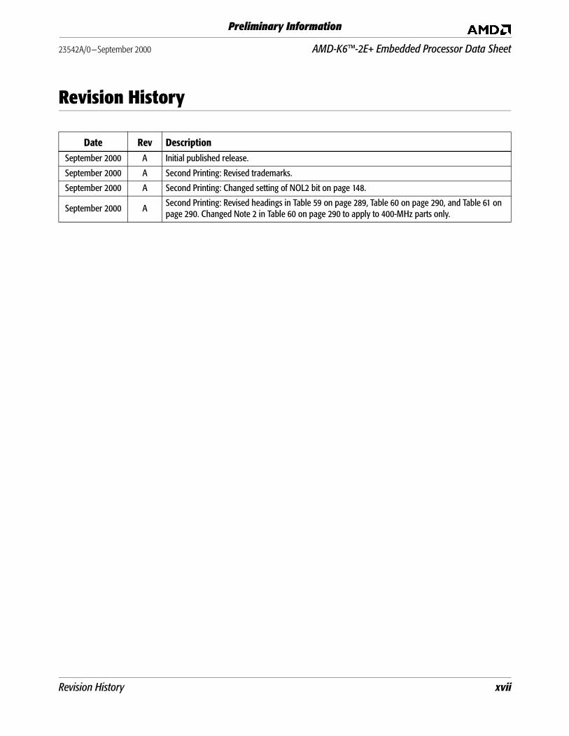
Date Rev DescriptionSeptember 2000 A Initial published release.
September 2000 A Second Printing: Revised trademarks.
September 2000 A Second Printing: Changed setting of NOL2 bit on page 148.
September 2000 ASecond Printing: Revised headings in Table 59 on page 289, Table 60 on page 290, and Table 61 on page 290. Changed Note 2 in Table 60 on page 290 to apply to 400-MHz parts only.
Revision History xvii

AMD-K6™-2E+ Embedded Processor Data Sheet 23542A/0—September 2000
Preliminary Information
xviii Revision History
23542A/0—September 2000 AMD-K6™-2E+ Embedded Processor Data Sheet
Preliminary Information
About this Data Sheet
The AMD-K6™-2E+ Embedded Processor Data Sheet is thecomplete specification of the AMD-K6™-2E+ embeddedprocessor.
Overview
This data sheet is organized into the following sections:
Chapter 1, “AMD-K6™-2E+ Embedded Processor” on page 1,provides a list of the AMD-K6-2E+ processor’s distinguishingcharacteristics, a description of the key features, and adiscussion about the Super7™ platform initiative.
Chapter 2, “Internal Architecture” on page 11, describes thefunctional elements of the advanced design techniques, knownas the RISC86® microarchitecture, implemented by theAMD-K6-2E+ processor.
Chapter 3, “Software Environment” on page 27, provides ageneral overview of the AMD-K6-2E processor’s x86 softwareenvironment and briefly describes the data types, registers,operating modes, interrupts, and instructions supported by theAMD-K6-2E+ processor ’s archi tecture and des ignimplementation.
Chapter 4, “Logic Symbol Diagram” on page 91, contains theAMD-K6-2E+ processor logic symbol diagram.
Chapter 5, “Signal Descriptions” on page 93, lists the signalsand their descriptions alphabetically and by function.
Chapter 6, “AMD PowerNow!™ Technology” on page 143,describes the enhanced power management features availableon the low-power versions of the AMD-K6-2E+ processor.
Chapter 7, “Bus Cycles” on page 153, describes and illustratesthe timing and relationship of bus signals during various typesof bus cycles.
About this Data Sheet xix
AMD-K6™-2E+ Embedded Processor Data Sheet 23542A/0—September 2000
Preliminary Information
Chapter 8, “Power-on Configuration and Initialization” onpage 199, describes how the system logic resets theAMD-K6-2E+ processor using the RESET signal.
Chapter 9, “Cache Organization” on page 205, describes thebasic architecture and resources of the AMD-K6-2E+processor’s internal caches.
Chapter 10, “Write Merge Buffer” on page 229, describes the 8-byte write merge buffer and how merging multiple write cyclesinto a single write cycle ultimately increases overall systemperformance.
Chapter 11, “Floating-Point and Multimedia Execution Units”on page 237, describes the AMD-K6-2E+ processor’s IEEE 754-compatible and 854-compatible floating point execution unit,the multimedia and 3DNow!™ technology execution units, andthe floating-point and MMX™/3DNow! technology instructioncompatibility.
Chapter 12, “System Management Mode (SMM)” on page 241,describes SMM, the state-save area, entry into and exit fromSMM, exceptions and interrupts in SMM, memory allocationand addressing in SMM, and the SMI# and SMIACT# signals.
Chapter 13, “Test and Debug” on page 251, describes thevarious test and debug modes that enable the functional andmanufacturing testing of systems and boards that use theAMD-K6-2E+ processor and that allow designers to debug theinstruction execution of software components.
Chapter 14, “Clock Control” on page 275, describes the fivemodes of clock control supported by the AMD-K6-2E+processor.
Chapter 15, “Electrical Data” on page 285, includes operatingranges, absolute ratings, DC characteristics, power dissipationdata, power and grounding information, and decouplingrecommendations.
Chapter 16, “Signal Switching Characteristics” on page 295,provides tables listing valid delay, float, setup, and hold timingspecifications for the AMD-K6-2E+ processor signals.
xx About this Data Sheet
23542A/0—September 2000 AMD-K6™-2E+ Embedded Processor Data Sheet
Preliminary Information
Chapter 17, “Thermal Design” on page 313, lists the packagethermal specifications, discusses how to measure casetemperature, and provides layout and airflow considerations.
Chapter 18, “Pin Designations” on page 321, provides top- andbottom-view connection diagrams for each package type andlists the AMD-K6-2E+ processor’s pin designations byfunctional grouping.
Chapter 19, “Package Specifications” on page 331, providesdiagrams showing the specifications for the 321-pin CPGApackage and the 349-ball OBGA package.
Chapter 20, “Ordering Information” on page 333, provides theordering part number (OPN) and valid OPN combinations.
About this Data Sheet xxi

AMD-K6™-2E+ Embedded Processor Data Sheet 23542A/0—September 2000
Preliminary Information
xxii About this Data Sheet
23542A/0—September 2000 AMD-K6™-2E+ Embedded Processor Data Sheet
Preliminary Information
1 AMD-K6™-2E+ Embedded Processor
The following are key features of the AMD-K6™-2E processor:
■ Member of the AMD-K6™E family of 32-bit embedded processors
◆ Brings the power, performance, and value of the AMD-K6 family to theembedded market
◆ Enables improved time-to-market by leveraging existing hardware and softwareinfrastructure and field-proven development tools
◆ Offers a wide software- and platform-compatible growth path with productlongevity to help preserve development investments
■ Functionally-compatible embedded version of the AMD-K6-2+ processor withinternal 128-Kbyte L2 cache
◆ Provides higher Super7™ platform performance with reduced total system cost
◆ Microsoft® Windows® compatible processor
◆ x86 binary software compatible
◆ Supports real-time operating systems such as pSOS, QNX, RTXC, and VxWorks
■ Advanced 6-issue RISC86® superscalar microarchitecture
◆ Ten parallel specialized execution units
◆ Multiple sophisticated x86-to-RISC86 instruction decoders
◆ Advanced two-level branch prediction
◆ Speculative and out-of-order execution
◆ Register renaming and data forwarding
◆ Up to six RISC86 instructions per clock
■ Innovative cache design
◆ 192-Kbyte total internal cache
• Internal split, two-way set associative, 64-Kbyte L1 Cache
- 32-Kbyte instruction cache with additional 20-Kbytes of predecode cache
- 32-Kbyte writeback dual-ported data cache
- MESI protocol support
• Internal full-speed, four-way set associative, 128-Kbyte, L2 Cache
◆ Multiport internal cache design enabling simultaneous 64-bit reads/writes ofL1 and L2 caches
■ Super7 platform is Socket 7-compatible
◆ Leverages high-speed 100-MHz processor bus
◆ 2x Accelerated Graphic Port (AGP) support
Chapter 1 AMD-K6™-2E+ Embedded Processor 1
AMD-K6™-2E+ Embedded Processor Data Sheet 23542A/0—September 2000
Preliminary Information
◆ Takes advantage of existing system support, logic integration, and designs forsuperior value
◆ Provides an easy upgrade path for embedded applications and a bridge tolegacy applications
■ AMD PowerNow!™ technology dynamically manages power and performance
◆ Monitors application requirements for performance or power utilization
◆ Supports continuously varying operating frequency and voltage, deliveringperformance on demand while dissipating the lowest amount of power possible
■ 3DNow!™ technology for better multimedia and audio performance
◆ x86 instruction set extension accelerates 3D graphics and other single-precision floating-point compute-intensive operations
◆ Offers fast frame rates on high-resolution graphics applications, superiormodeling of real-world environments and physics, life-like images andgraphics, and big-screen sound and video
◆ Additional 3DNow! technology DSP instructions enhance communicationsapplications
◆ Separate multiplier and ALU for superscalar instruction execution
■ High-performance IEEE 754-compatible and 854-compatible floating-point unit
■ High-performance industry-standard MMX™ instructions
◆ Dual-integer ALU for superscalar execution
■ Industry-standard System Management Mode (SMM)
■ IEEE 1149.1 boundary scan
■ 321-Pin Ceramic Pin Grid Array (CPGA) or 349-Ball Organic Ball Grid Array(OBGA) package
■ Low-voltage 0.18-micron process technology
◆ Split-plane power with support for full 3.3 V I/O
◆ Lower core voltages enable low-power operation
■ Operating frequencies
◆ Standard-power and standard-temperature devices: 400, 450, and 500 MHz
◆ Low-power and extended-temperature devices: 350, 400, and 450 MHz
2 AMD-K6™-2E+ Embedded Processor Chapter 1
23542A/0—September 2000 AMD-K6™-2E+ Embedded Processor Data Sheet
Preliminary Information
1.1 AMD-K6™-2E+ Embedded Processor Features
The innovative AMD-K6-2E+ processor brings industry-leading performance toembedded systems. Its Super7™ platform-compatible, 321-pin ceramic pin grid array(CPGA) or 349-ball organic ball grid array (OBGA) package enables embeddedsystem designers to reduce time-to-market by leveraging today’s cost-effective,industry-standard infrastructure.
Manufactured using AMD’s 0.18 micron low-power process, the AMD-K6-2E+processor incorporates the innovative and efficient RISC86® microarchitecture, a192-Kbyte total internal cache, a fast 100 MHz frontside bus, and a powerful IEEE754-compatible and 854-compatible floating-point execution unit. The AMD-K6-2E+processor also incorporates a superscalar MMX™ unit and AMD’s innovative 3DNow!technology for high-performance multimedia and 3D graphics operation.
The AMD-K6-2E+ processor is a functionally compatible embedded version of theAMD-K6-2+ processor with an internal 128-Kbyte L2 cache. The AMD-K6-2E+processor offers a clock-for-clock performance boost at a lower total system cost overexisting Socket 7 systems because no external L2 cache is required. The low-powerversions of the AMD-K6-2E+ processor also support AMD’s enhanced powermanagement features, called AMD PowerNow! technology.
The AMD-K6-2E+ processor is part of the AMD-K6E family of embedded processors.Within this family:
■ The AMD-K6-2E processor provides the best value and performance for cost-sensitive embedded applications.
■ The AMD-K6-2E+ with its 128-Kbyte internal L2 cache offers higher performancebalanced with cost.
■ The AMD-K6-IIIE+ with its 256-Kbyte internal L2 cache offers the highestperformance available for Super7 and Socket 7 platforms.
All AMD-K6E family processors in the CPGA package share the same footprint andsupport the Socket 7-compatible Super7 platform. The AMD-K6E family providesembedded designers with an assured growth plan and supply stability, along withproduct longevity. All AMD-K6E family processors are x86-binary compatible,allowing preservation of the initial software investment.
The AMD-K6-2E+ embedded processor is particularly well-suited for use inapplications where high performance is required. It is designed to offer compelling,yet affordable, power and performance for high-end embedded applications, such asinformation appliances, set-top boxes, embedded PCs, point-of-sale terminals, publicand private communications infrastructure, and industrial control.
Chapter 1 AMD-K6™-2E+ Embedded Processor 3
AMD-K6™-2E+ Embedded Processor Data Sheet 23542A/0—September 2000
Preliminary Information
The AMD-K6-2E+ embedded processor is available in two versions.
■ The low-power version operates at the lowest core voltage in order to offer thelowest available power and extended temperature ratings. Enhanced powermanagement features are provided via AMD PowerNow! technology in the low-power versions of the processor.
■ The standard-power version has a 2.0-V core voltage and offers standard powerand temperature specifications similar to desktop PC processors.
Innovative Cache Design for Faster Data Access
Recognizing the benefits of a large and fast cache design in feeding performance-hungry applications, AMD developed an innovative cache architecture that enhancesthe performance available for embedded applications based on the Super7 platform.
AMD’s cache design innovations include:
■ An internal 128-Kbyte L2 write-back cache operating at the full speed of theprocessor and complementing the 64-Kbyte L1 cache, which is standard in allAMD-K6 family processors.
■ A multiport internal cache design, enabling simultaneous 64-bit reads and writesto both the L1 cache and the L2 cache.
■ A 4-way set associative backside L2 cache design enabling optimal datamanagement and external frontside data bus bandwidth efficiency.
The processor's multiport internal cache design enables both the 64-Kbyte L1 cacheand the 128-Kbyte L2 cache to perform simultaneous 64-bit read and write operationsin a clock cycle. This multiport capability allows data to be processed faster and moreefficiently than non-multiported designs. In addition, the processor core can accessboth L1 and L2 caches simultaneously, which further enhances overall CPUthroughput.
The cache design is exceptionally fast, with the backside 128-Kbyte L2 cacheoperating at full processor speed.
For example, the internal L2 cache of an AMD-K6-2E+/450 processor operates at 450MHz and provides nine times the peak bandwidth of an external L2 cache operatingat 100 MHz. The maximum peak bandwidth of an external L2 cache operating at 100MHz is 800 Mbytes/s, while an internal L2 cache operating at 450 MHz delivers amaximum peak bandwidth of 3,600 Mbytes/s per port. Because the internal L2 cacheof the AMD-K6-2E+ processor is dual-ported for simultaneous reads and writes, thetotal peak bandwidth is doubled to 7,200 Mbytes/s, resulting in a maximum peakbandwidth nine times as large as a 100-MHz cache implementation.
4 AMD-K6™-2E+ Embedded Processor Chapter 1
23542A/0—September 2000 AMD-K6™-2E+ Embedded Processor Data Sheet
Preliminary Information
3DNow!™ Technology
The AMD-K6-2E+ processor supports AMD’s 3DNow! technology, an extension to thex86 instruction set that includes 21 new instructions to accelerate 3D graphics andother single-precision floating-point compute intensive operations.
3DNow! technology was defined and implemented in collaboration with Microsoft,application developers, and graphics vendors, and has received an enthusiasticreception. It is compatible with today’s existing x86 software and requires nooperating system support, thereby enabling a broad class of applications to benefitfrom 3DNow! technology.
The worldwide installed base of 3DNow! technology-enhanced PCs has grown to morethan 25 million desktop and notebook systems, revolutionizing the 3D experiencewith up to four times the peak floating-point performance of previous sixthgeneration solutions. Support for 3DNow! technology exists today in leading industry-standard APIs, including Microsoft® DirectX and SGI’s OpenGL APIs. Additionally,numerous hardware and software products have been optimized for 3DNow!technology. AMD is now bringing this advanced capability to embedded systems.
3DNow! technology enables fast frame rates on high-resolution 3D-rendered scenes,realistic physical modeling of real-world environments, sharp and detailed 3Dimaging, smooth video playback, and theater-quality audio.
In addition, the AMD-K6-2E+ processor adds support for five new digital signalprocessing (DSP) instructions, developed to enhance the performance ofcommunications applications, including soft xDSL modems, MP3 recording, andDolby Digital and Surround Sound processing.
Chapter 1 AMD-K6™-2E+ Embedded Processor 5

AMD-K6™-2E+ Embedded Processor Data Sheet 23542A/0—September 2000
Preliminary Information
AMD PowerNow!™ Technology for Enhanced Power Management
AMD has added a number of new power management features to the low-powerversions of the AMD-K6-2E+ processor. Collectively, these hardware and softwarefeatures are called AMD PowerNow!™ technology.
AMD PowerNow! technology allows the AMD-K6-2E+ processor to run at differentfrequencies and voltages, depending on the application’s need for maximumperformance or the most efficient power utilization.
AMD PowerNow! technology includes AMD’s unique “automatic mode” feature, whichallows the system to monitor application usage and to continuously vary the operatingfrequency and voltage, delivering performance on demand while dissipating thelowest amount of power possible.
■ When application demands require the processor to run at maximumperformance, the AMD PowerNow! technology steps up the performance to meetthe demand.
■ As platform demand for performance subsides, AMD PowerNow! technology candynamically drop into a lower power state.
AMD PowerNow! technology enables embedded products to dynamically managepower and performance.
System Management Mode and Other Power Management Features
The AMD-K6-2E+ processor includes the complete industry-standard systemmanagement mode (SMM), which is critical to system resource and powermanagement.
The AMD-K6-2E+ processor also features the industry-standard Stop-Clock(STPCLK#) control circuitry and the Halt instruction, both required forimplementing the ACPI power management specification.
Microarchitecture
The AMD-K6-2E+ processor’s 6-issue RISC86 microarchitecture is a decoupleddecode/execution superscalar design that implements state-of-the-art designtechniques to achieve leading-edge performance.
Advanced design techniques implemented in the AMD-K6-2E+ processor includemultiple x86 instruction decode, single-clock internal RISC operations, ten executionunits that support superscalar operation, out-of-order execution, data forwarding,speculative execution, and register renaming.
6 AMD-K6™-2E+ Embedded Processor Chapter 1
23542A/0—September 2000 AMD-K6™-2E+ Embedded Processor Data Sheet
Preliminary Information
In addition, the processor supports advanced branch prediction logic byimplementing an 8192-entry branch history table, a branch target cache, and a returnaddress stack, which combine to deliver better than a 95% prediction rate. Thesedesign techniques enable the AMD-K6-2E+ processor to issue, execute, and retiremultiple x86 instructions per clock, resulting in excellent scaleable performance.
Industry-Standard x86 Architecture
The AMD-K6-2E+ processor is x86 binary code compatible. AMD’s extensiveexperience through six generations of x86 processors has been carefully integratedinto the processor to enable compatibility with Windows® 98, Windows 95, Windows3.x, Windows NT, DOS, Linux, OS/2, Unix, Solaris, NetWare®, and other leading x86operating systems and applications. The AMD-K6-2E+ processor is also compatiblewith leading real-time operating systems (RTOS) commonly used in embeddedapplications, such as pSOS, QNX, RTXC, and VxWorks. Additionally, the AMDFusionE86SM third-party tool support program offers extensive development supportfor AMD-K6-2E+ processor designs.
The AMD-K6-2E+ processor is Super7 and Socket 7-compatible. The Super7 platformis an extension to the popular and robust Socket 7 platform. See “Super7™ Platform”on page 8 for more information.
AMD is the world’s second-leading supplier of PC processors compatible with theWindows operating system, having shipped more than 120 mill ion x86microprocessors, including more than 60 million Windows-compatible processors. TheAMD-K6-2E+ processor for embedded applications is the latest member in this longline of processors. With its combination of state-of-the-art features, industry-leadingperformance, high-performance 3DNow! technology and multimedia engines, x86compatibility, and low-cost infrastructure, the AMD-K6-2E+ processor is the superiorchoice for high-performance embedded systems.
1.2 Process Technology
The AMD-K6-2E+ processor is implemented using an AMD-developed, state-of-the-artlow power 0.18-micron process technology. This process technology features a split-plane design that enables the AMD-K6-2E+ processor to deliver excellentperformance solutions while utilizing a lower processor core voltage, which results inlower power consumption, while the I/O portion operates at the industry-standard3.3-V level.
Chapter 1 AMD-K6™-2E+ Embedded Processor 7
AMD-K6™-2E+ Embedded Processor Data Sheet 23542A/0—September 2000
Preliminary Information
1.3 Super7™ Platform
The Super7 platform is an extension to the popular Socket 7 platform. AMD and itsindustry partners have invested in the future of Socket 7 with the Super7 platforminitiative. The goal of the initiative is to maintain the competitive vitality of theSocket 7 infrastructure through a series of enhancements, including the developmentof an industry-standard 100-MHz processor bus protocol.
In addition to the 100-MHz processor bus protocol, the Super7 initiative includes theintroduction of chipsets that support the AGP specification, and support for abackside L2 cache. Currently, over 40 motherboard vendors and all major BIOS andchipset vendors offer Super7-based products.
All AMD-K6 embedded processors in CPGA packages remain pin compatible withexisting Socket 7 solutions; however, for maximum system performance, theAMD-K6-2E+processor works optimally in Super7 designs that incorporate advancedfeatures such as support for the 100-MHz frontside bus and AGP graphics.
100-MHz Processor Bus
The AMD-K6-2E+ processor supports a 100-MHz, 800 Mbyte/second frontside bus toprovide a high-speed interface to Super7 platform-based chipsets. The 100-MHzinterface speeds up access to main memory by 50 percent over the 66-MHz Socket 7interface — resulting in a significant 10 percent increase in overall systemperformance.
Accelerated Graphics Port Support
Accelerated Graphics Port (AGP) support improves the performance of videographics systems that have small amounts of video memory on the graphics card. Theindustry-standard AGP specification enables a 133-MHz graphics interface and willscale to even higher levels of performance.
Support For Backside L2 Cache
The Super7 platform has the ‘headroom’ to support higher-performance AMD-K6processors like the AMD-K6-2E+ processor, which features a full-speed, internalbackside 128-Kbyte L2 cache designed to enable new levels of performance toleading-edge embedded systems.
8 AMD-K6™-2E+ Embedded Processor Chapter 1

23542A/0—September 2000 AMD-K6™-2E+ Embedded Processor Data Sheet
Preliminary Information
Super7™ Platform Advantages
The Super7 platform:
■ Delivers performance and features competitive with alternate platforms at thesame clock speed, and at a significantly lower cost
■ Takes advantage of existing system designs for superior value
■ Enables OEMs and resellers to take advantage of mature, high-volumeinfrastructure supported by multiple BIOS, chipset, graphics, and motherboardsuppliers
■ Reduces inventory and design costs with one motherboard for a wide range ofproducts
■ Builds on a huge installed base of more than 100 million motherboards
■ Provides an easy upgrade path for embedded applications, as well as a bridge tolegacy applications
By taking advantage of the low-cost, mature Socket 7 infrastructure, the Super7platform will continue to provide superior value and leading-edge performance forembedded systems.
Chapter 1 AMD-K6™-2E+ Embedded Processor 9
AMD-K6™-2E+ Embedded Processor Data Sheet 23542A/0—September 2000
Preliminary Information
10 AMD-K6™-2E+ Embedded Processor Chapter 1
23542A/0—September 2000 AMD-K6™-2E+ Embedded Processor Data Sheet
Preliminary Information
2 Internal Architecture
The AMD-K6-2E+ processor implements advanced designtechniques known as the RISC86 microarchitecture. TheRISC86 microarchitecture is a decoupled decode/executiondesign approach that yields superior sixth-generationperformance for x86-based software. This chapter describes thetechniques used and the functional elements of the RISC86microarchitecture.
2.1 Microarchitecture Overview
When discussing processor design, it is important to understandthe terms architecture , microarchitecture , and designimplementation.
■ Architecture refers to the instruction set and features of aprocessor that are visible to software programs running onthe processor. The architecture determines what softwarethe processor can run. The architecture of the AMD-K6-2E+processor is the industry-standard x86 instruction set.
■ Microarchitecture refers to the design techniques used in theprocessor to reach the target cost, performance, andfunctionality goals. The AMD-K6 family of processors arebased on a sophisticated RISC core known as the EnhancedRISC86 microarchitecture. The Enhanced RISC86microarchitecture is an advanced, second-order decoupleddecode/execution design approach that enablesindustry-leading performance for x86-based software.
■ Design implementation refers to the actual logic and circuitdesigns from which the processor is created according to themicroarchitecture specifications.
Chapter 2 Internal Architecture 11
AMD-K6™-2E+ Embedded Processor Data Sheet 23542A/0—September 2000
Preliminary Information
Enhanced RISC86® Microarchitecture
The Enhanced RISC86 microarchitecture defines thecharacteristics of the AMD-K6 family of processors. Theinnovative RISC86 microarchitecture approach implements thex86 instruction set by internally translating x86 instructionsinto RISC86 operations. These RISC86 operations werespecially designed to include direct support for the x86instruction set while observing the RISC performanceprinciples of fixed length encoding, regularized instructionfields, and a large register set.
The Enhanced RISC86 microarchitecture used in theAMD-K6-2E+ processor enables higher processor coreperformance and promotes straightforward extensions, such asthose added in the current AMD-K6-2E+ processor and thoseplanned for the future. Instead of directly executing complexx86 instructions, which have lengths of 1 to 15 bytes, theAMD-K6-2E+ processor executes the simpler and easierfixed-length RISC86 operations, while maintaining theinstruction coding efficiencies found in x86 programs.
The AMD-K6-2E+ processor contains parallel decoders, acentralized RISC86 operation scheduler, and ten executionunits that support superscalar operation—multiple decode,execution, and retirement—of x86 instructions. These elementsare packed into an aggressive and highly efficient six-stagepipeline.
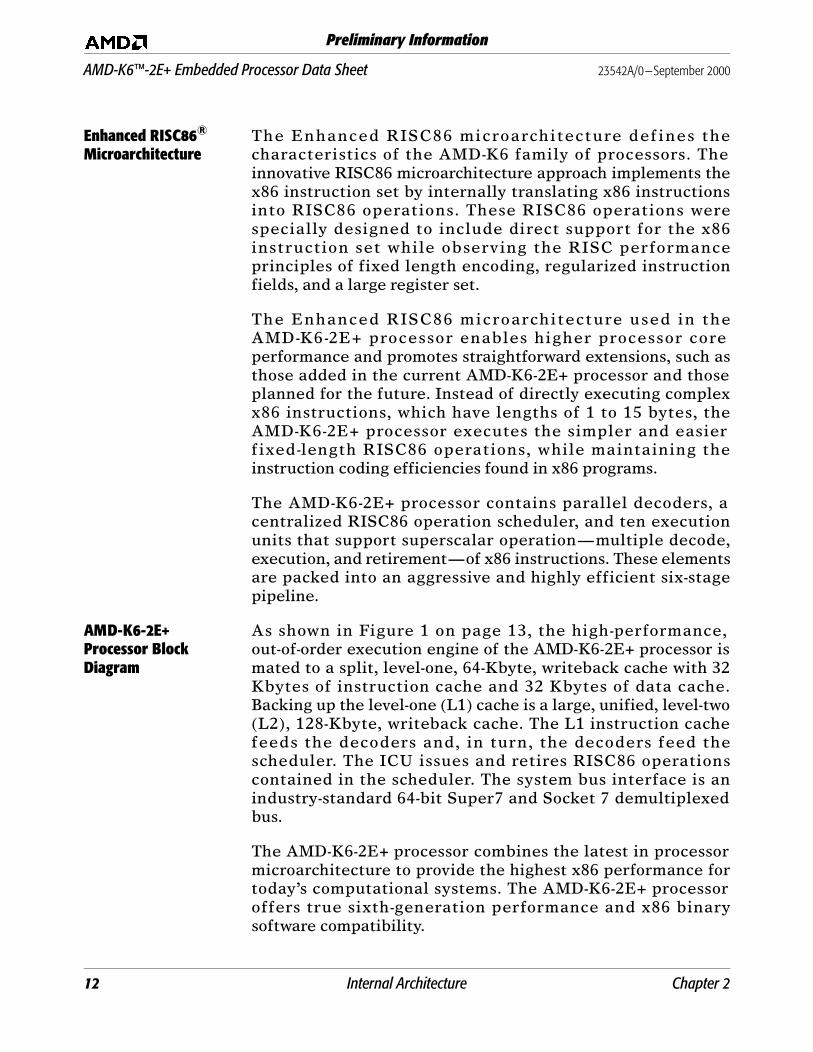
AMD-K6-2E+ Processor Block Diagram
As shown in Figure 1 on page 13, the high-performance,out-of-order execution engine of the AMD-K6-2E+ processor ismated to a split, level-one, 64-Kbyte, writeback cache with 32Kbytes of instruction cache and 32 Kbytes of data cache.Backing up the level-one (L1) cache is a large, unified, level-two(L2), 128-Kbyte, writeback cache. The L1 instruction cachefeeds the decoders and, in turn, the decoders feed thescheduler. The ICU issues and retires RISC86 operationscontained in the scheduler. The system bus interface is anindustry-standard 64-bit Super7 and Socket 7 demultiplexedbus.
The AMD-K6-2E+ processor combines the latest in processormicroarchitecture to provide the highest x86 performance fortoday’s computational systems. The AMD-K6-2E+ processoroffers true sixth-generation performance and x86 binarysoftware compatibility.
12 Internal Architecture Chapter 2

23542A/0—September 2000 AMD-K6™-2E+ Embedded Processor Data Sheet
Preliminary Information
Figure 1. AMD-K6™-2E+ Processor Block Diagram
Decoders Decoding of the x86 instructions begins when the on-chip L1instruction cache is filled. Predecode logic determines thelength of an x86 instruction on a byte-by-byte basis. Thispredecode information is stored, along with the x86instructions, in the L1 instruction cache, to be used later by thedecoders. The decoders translate on-the-fly, with no additionallatency, up to two x86 instructions per clock into RISC86operations.
Note: In this chapter, “clock” refers to a processor clock.
The AMD-K6-2E+ processor categorizes x86 instructions intothree types of decodes—short, long, and vector. The decodersprocess either two short, one long, or one vector decode at atime.
The three types of decodes have the following characteristics:
■ Short decodes—x86 instructions less than or equal to sevenbytes in length
6WRUH8QLW
6WRUH4XHXH
,QVWUXFWLRQ&RQWURO�8QLW
6FKHGXOHU%XIIHU
����5,6&���6L[�5,6&��6L[�5,6&����
2SHUDWLRQ�,VVXH2SHUDWLRQ�,VVXH
)RXU��5,6&��'HFRGH
2XW�RI�2UGHU2XW�RI�2UGHU([HFXWLRQ�(QJLQH([HFXWLRQ�(QJLQH
/HYHO�2QH�'XDO�3RUW�'DWD�&DFKH�����.%\WH�
����(QWU\�'7/%
���.%\WH�/HYHO�2QH�,QVWUXFWLRQ�&DFKH
���.%\WH�3UHGHFRGH�&DFKH
'XDO�,QVWUXFWLRQ�'HFRGHUV[���WR�5,6&��
���%\WH�)HWFK
/RDG8QLW
)ORDWLQJ��3RLQW8QLW
%UDQFK5HVROXWLRQ�8QLW
3UHGHFRGH/RJLF
/HYHO�2QH�&DFKH&RQWUROOHU
����0+]6XSHU��
%XV,QWHUIDFH
/HYHO�7ZR&DFKH
�����.%\WH�5HJLVWHU�8QLW�;
�,QWHJHU�0XOWLPHGLD��'1RZ�70�
5HJLVWHU�8QLW�<�,QWHJHU�
0XOWLPHGLD��'1RZ��
%UDQFK�/RJLF������(QWU\�%+7�����(QWU\�%7&�����(QWU\�5$6�
���(QWU\�,7/%
Chapter 2 Internal Architecture 13
AMD-K6™-2E+ Embedded Processor Data Sheet 23542A/0—September 2000
Preliminary Information
■ Long decodes—x86 instructions less than or equal to 11bytes in length
■ Vector decodes—complex x86 instructions
Short and long decodes are processed completely within thedecoders. Vector decodes are started by the decoders and thencompleted by fetched sequences from an on-chip ROM. Afterdecoding, the RISC86 operations are delivered to the schedulerfor dispatching to the executions units.
Scheduler/Instruction Control Unit
The centralized scheduler or buffer is managed by theInstruction Control Unit (ICU). The ICU buffers and managesup to 24 RISC86 operations at a time. This equals from 6 to 12x86 instructions. This buffer size (24) is perfectly matched tothe processor ’s s ix -s tage RISC86 pipel ine and fourRISC86-operations decode rate.
The scheduler accepts as many as four RISC86 operations at atime from the decoders and retires up to four RISC86operat ions per c lock cyc le . The ICU is capable ofsimultaneously issuing up to six RISC86 operations at a time tothe execution units. This consists of the following types ofoperations:
■ Memory load operation
■ Memory store operation
■ Complex integer, MMX or 3DNow! register operation
■ Simple integer, MMX or 3DNow! register operation
■ Floating-point register operation
■ Branch condition evaluation
Registers When managing the RISC86 operations, the ICU uses 69physical regis ters contained within the RISC86microarchitecture.
■ Forty-eight of the physical registers are located in a generalregister file.
• Twenty-four of these are rename registers.
• The other twenty-four are committed or architecturalregisters, consisting of 16 scratch registers and 8 registersthat correspond to the x86 general-purpose registers—EAX, EBX, ECX, EDX, EBP, ESP, ESI, and EDI.
14 Internal Architecture Chapter 2

23542A/0—September 2000 AMD-K6™-2E+ Embedded Processor Data Sheet
Preliminary Information
■ An analogous set of 21 registers is available specifically forMMX and 3DNow! operations.
• Twelve of these are MMX/3DNow! rename registers.
■ Nine are MMX/3DNow! committed or architectural registers,consisting of one scratch register and eight registers thatcorrespond to the MMX registers (mm0–mm7, as shown inFigure 17 on page 35.
Branch Logic The AMD-K6-2E+ processor is designed with highlysophisticated dynamic branch logic consisting of the following:
■ Branch history/prediction table
■ Branch target cache
■ Return address stack
The AMD-K6-2E+ processor implements a two-level branchprediction scheme based on an 8192-entry branch history table.The branch history table stores prediction information that isused for predicting conditional branches. Because the branchhistory table does not store predicted target addresses, specialaddress ALUs calculate target addresses on the fly duringinstruction decode.
The branch target cache augments predicted branchperformance by avoiding a one clock cache-fetch penalty. Thisspecialized target cache does this by supplying the first 16 bytesof target instructions to the decoders when branches arepredicted. The return address stack is a unique devicespecifically designed for optimizing CALL and RETURN pairs.In summary, the AMD-K6-2E+ processor uses dynamic branchlogic to minimize delays due to the branch instructions that arecommon in x86 software.
3DNow!™ Technology AMD has taken a lead role in improving the multimedia and 3Dcapabilities of the x86 processor family with the introduction of3DNow! technology, which uses a packed, single-precision,floating-point data format and Single Instruction Multiple Data(SIMD) operations based on the MMX technology model.
Chapter 2 Internal Architecture 15
AMD-K6™-2E+ Embedded Processor Data Sheet 23542A/0—September 2000
Preliminary Information
2.2 Cache, Instruction Prefetch, and Predecode Bits
The writeback level-one (L1) cache on the AMD-K6-2E+processor is organized as a separate 32-Kbyte instruction cacheand a 32-Kbyte data cache with two-way set associativity.
The level-two (L2) cache is 128 Kbytes, and is organized as aunified, four-way set-associative cache. The cache line size is 32bytes, and lines are fetched from external memory using anefficient pipelined burst transaction.
As the L1 instruction cache is filled from the L2 cache or fromexternal memory, each instruction byte is analyzed forinstruction boundaries using predecoding logic. Predecodingannotates information (5 bits per byte) to each instruction bytethat later enables the decoders to efficiently decode multipleinstructions simultaneously.
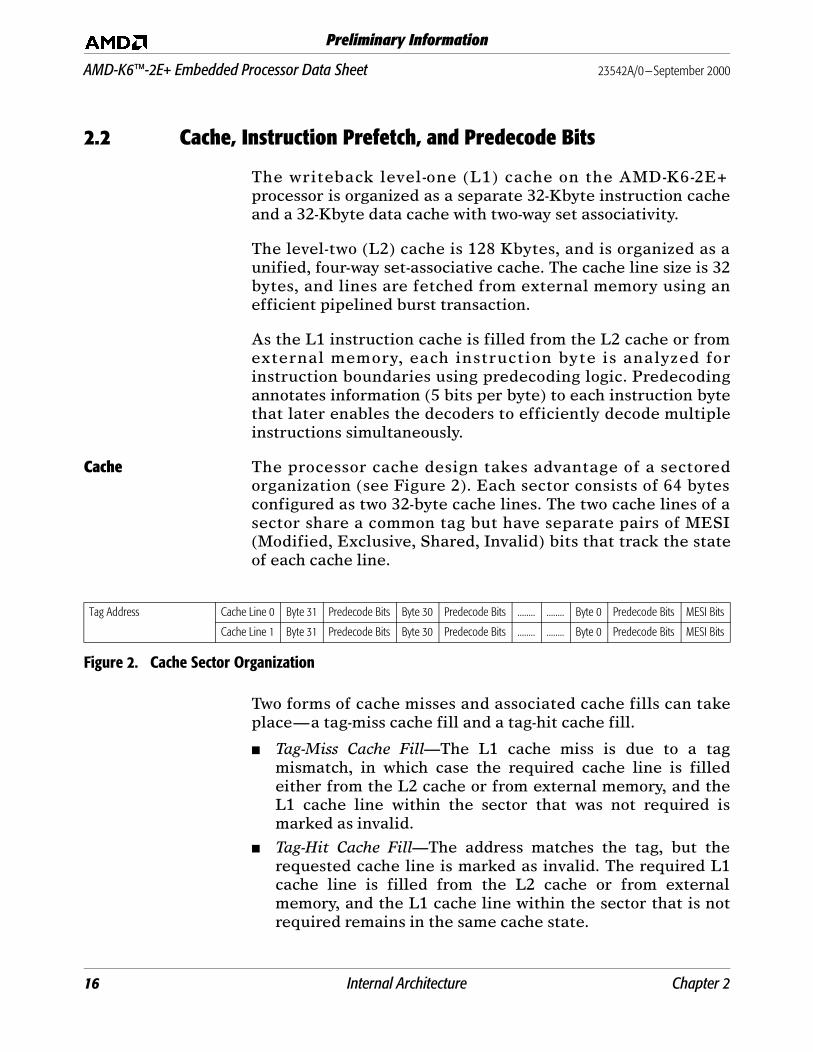
Cache The processor cache design takes advantage of a sectoredorganization (see Figure 2). Each sector consists of 64 bytesconfigured as two 32-byte cache lines. The two cache lines of asector share a common tag but have separate pairs of MESI(Modified, Exclusive, Shared, Invalid) bits that track the stateof each cache line.
Figure 2. Cache Sector Organization
Two forms of cache misses and associated cache fills can takeplace—a tag-miss cache fill and a tag-hit cache fill.
■ Tag-Miss Cache Fill—The L1 cache miss is due to a tagmismatch, in which case the required cache line is filledeither from the L2 cache or from external memory, and theL1 cache line within the sector that was not required ismarked as invalid.
■ Tag-Hit Cache Fill—The address matches the tag, but therequested cache line is marked as invalid. The required L1cache line is filled from the L2 cache or from externalmemory, and the L1 cache line within the sector that is notrequired remains in the same cache state.
Tag Address Cache Line 0 Byte 31 Predecode Bits Byte 30 Predecode Bits ........ ........ Byte 0 Predecode Bits MESI Bits
Cache Line 1 Byte 31 Predecode Bits Byte 30 Predecode Bits ........ ........ Byte 0 Predecode Bits MESI Bits
16 Internal Architecture Chapter 2
23542A/0—September 2000 AMD-K6™-2E+ Embedded Processor Data Sheet
Preliminary Information
Prefetching The AMD-K6-2E+ processor conditionally performs cacheprefetching, which results in the filling of the required cacheline first, and a prefetch of the second cache line making up theother half of the sector. From the perspective of the externalbus, the two cache-line fills typically appear as two 32-byteburst read cycles occurring back-to-back or, if allowed, aspipelined cycles.
The 3DNow! technology includes an instruction calledPREFETCH that allows a cache line to be prefetched into theL1 data cache and the L2 cache. The PREFETCH instructionformat is defined in Table 15, “3DNow!™ Instructions,” onpage 89. For more detailed information, see the 3DNow!™Technology Manual, order# 21928.
Predecode Bits Decoding x86 instructions is particularly difficult because theinstructions are variable-length and can be from 1 to 15 byteslong. Predecode logic supplies the five predecode bits that areassociated with each instruction byte. The predecode bitsindicate the number of bytes to the start of the next x86instruction. The predecode bits are stored in an extendedinstruction cache alongside each x86 instruction byte as shownin Figure 2 on page 16. The predecode bits are passed with theinstruction bytes to the decoders where they assist with parallelx86 instruction decoding.
2.3 Instruction Fetch and Decode
Instruction Fetch The processor can fetch up to 16 bytes per clock out of the L1instruction cache or branch target cache. The fetchedinformation is placed into a 16-byte instruction buffer thatfeeds directly into the decoders (see Figure 3 on page 18).Fetching can occur along a single execution stream with up toseven outstanding branches taken.
The instruction fetch logic is capable of retrieving any 16contiguous bytes of information within a 32-byte boundary.There is no additional penalty when the 16 bytes of instructionslie across a cache line boundary. The instruction bytes areloaded into the instruction buffer as they are consumed by thedecoders.
Although instructions can be consumed with byte granularity,the instruction buffer is managed on a memory-aligned word
Chapter 2 Internal Architecture 17
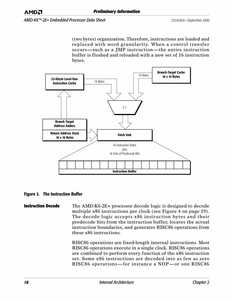
AMD-K6™-2E+ Embedded Processor Data Sheet 23542A/0—September 2000
Preliminary Information
(two bytes) organization. Therefore, instructions are loaded andreplaced with word granularity. When a control transferoccurs—such as a JMP instruction—the entire instructionbuffer is flushed and reloaded with a new set of 16 instructionbytes.
Figure 3. The Instruction Buffer
Instruction Decode The AMD-K6-2E+ processor decode logic is designed to decodemultiple x86 instructions per clock (see Figure 4 on page 19).The decode logic accepts x86 instruction bytes and theirpredecode bits from the instruction buffer, locates the actualinstruction boundaries, and generates RISC86 operations fromthese x86 instructions.
RISC86 operations are fixed-length internal instructions. MostRISC86 operations execute in a single clock. RISC86 operationsare combined to perform every function of the x86 instructionset. Some x86 instructions are decoded into as few as zeroRISC86 operations — for instance a NOP — or one RISC86
16 Instruction Bytesplus
16 Sets of Predecode Bits
Branch-Target Cache16 x 16 Bytes
2:1
Instruction Buffer
16 Bytes
16 Bytes
Branch TargetAddress Adders
Return Address Stack16 x 16 Bytes
32-Kbyte Level-OneInstruction Cache
Fetch Unit
18 Internal Architecture Chapter 2
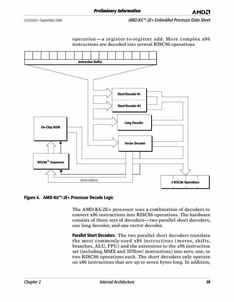
23542A/0—September 2000 AMD-K6™-2E+ Embedded Processor Data Sheet
Preliminary Information
operation — a register-to-register add. More complex x86instructions are decoded into several RISC86 operations.
Figure 4. AMD-K6™-2E+ Processor Decode Logic
The AMD-K6-2E+ processor uses a combination of decoders toconvert x86 instructions into RISC86 operations. The hardwareconsists of three sets of decoders—two parallel short decoders,one long decoder, and one vector decoder.
Parallel Short Decoders. The two parallel short decoders translatethe most commonly-used x86 instructions ( moves, shifts,branches, ALU, FPU) and the extensions to the x86 instructionset (including MMX and 3DNow! instructions) into zero, one, ortwo RISC86 operations each. The short decoders only operateon x86 instructions that are up to seven bytes long. In addition,
Instruction Buffer
4 RISC86 Operations
Long Decoder
Short Decoder #1
Short Decoder #2
Vector Address
Vector Decoder
RISC86® Sequencer
On-Chip ROM
Chapter 2 Internal Architecture 19

AMD-K6™-2E+ Embedded Processor Data Sheet 23542A/0—September 2000
Preliminary Information
they are designed to decode up to two x86 instructions perclock.
Long Decoder. The commonly-used x86 instructions that aregreater than seven bytes but not more than 11 bytes long andless-commonly-used x86 instructions that are up to seven byteslong are handled by the long decoder. The long decoder onlyperforms one decode per clock and generates up to four RISC86operations.
Vector Decoder. All other translations (complex instructions,serializing conditions, interrupts and exceptions, etc.) arehandled by a combination of the vector decoder and RISC86operation sequences fetched from an on-chip ROM. Forcomplex operations, the vector decoder logic provides the firstset of RISC86 operations and a vector (initial ROM address) to asequence of further RISC86 operations. The same types ofRISC86 operations are fetched from the ROM as those that aregenerated by the hardware decoders.
Note: Although all three sets of decoders are simultaneously fed acopy of the instruction buffer contents, only one of the threetypes of decoders is used during any one decode clock.
Grouped Operations. The decoders or the on-chip RISC86 ROMalways generate a group of four RISC86 operations. For decodesthat cannot fill the entire group with four RISC86 operations,RISC86 NOP operations are placed in the empty locations ofthe grouping. For example, a long-decoded x86 instruction thatconverts to only three RISC86 operations is padded with asingle RISC86 NOP operation and then passed to the scheduler.Up to six groups or 24 RISC86 operations can be placed in thescheduler at a time.
Floating Point Instructions. All of the common, and a few of theuncommon, floating-point instructions (also known as ESCinstructions) are hardware decoded as short decodes. Thisdecode generates a RISC86 floating-point operation and,optionally, an associated floating-point load or store operation.Floating-point or ESC instruction decode is only allowed in thefirst short decoder, but non-ESC instructions can be decodedsimultaneously by the second short decoder along with an ESCinstruction decode in the first short decoder.
20 Internal Architecture Chapter 2
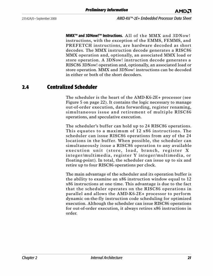
23542A/0—September 2000 AMD-K6™-2E+ Embedded Processor Data Sheet
Preliminary Information
MMX™ and 3DNow!™ Instructions. All of the MMX and 3DNow!instructions, with the exception of the EMMS, FEMMS, andPREFETCH instructions, are hardware decoded as shortdecodes. The MMX instruction decode generates a RISC86MMX operation and, optionally, an associated MMX load orstore operation. A 3DNow! instruction decode generates aRISC86 3DNow! operation and, optionally, an associated load orstore operation. MMX and 3DNow! instructions can be decodedin either or both of the short decoders.
2.4 Centralized Scheduler
The scheduler is the heart of the AMD-K6-2E+ processor (seeFigure 5 on page 22). It contains the logic necessary to manageout-of-order execution, data forwarding, register renaming,simultaneous issue and retirement of multiple RISC86operations, and speculative execution.
The scheduler’s buffer can hold up to 24 RISC86 operations.This equates to a maximum of 12 x86 instructions. Thescheduler can issue RISC86 operations from any of the 24locations in the buffer. When possible, the scheduler cansimultaneously issue a RISC86 operation to any availableexecut ion unit ( s tore , load, branch , regis ter Xinteger/multimedia, register Y integer/multimedia, orfloating-point). In total, the scheduler can issue up to six andretire up to four RISC86 operations per clock.
The main advantage of the scheduler and its operation buffer isthe ability to examine an x86 instruction window equal to 12x86 instructions at one time. This advantage is due to the factthat the scheduler operates on the RISC86 operations inparallel and allows the AMD-K6-2E+ processor to performdynamic on-the-fly instruction code scheduling for optimizedexecution. Although the scheduler can issue RISC86 operationsfor out-of-order execution, it always retires x86 instructions inorder.
Chapter 2 Internal Architecture 21
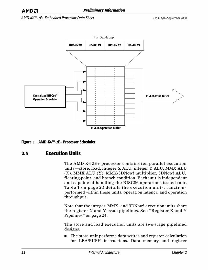
AMD-K6™-2E+ Embedded Processor Data Sheet 23542A/0—September 2000
Preliminary Information
Figure 5. AMD-K6™-2E+ Processor Scheduler
2.5 Execution Units
The AMD-K6-2E+ processor contains ten parallel executionunits—store, load, integer X ALU, integer Y ALU, MMX ALU(X), MMX ALU (Y), MMX/3DNow! multiplier, 3DNow! ALU,floating-point, and branch condition. Each unit is independentand capable of handling the RISC86 operations issued to it.Table 1 on page 23 details the execution units, functionsperformed within these units, operation latency, and operationthroughput.
Note that the integer, MMX, and 3DNow! execution units sharethe register X and Y issue pipelines. See “Register X and YPipelines” on page 24.
The store and load execution units are two-stage pipelineddesigns.
■ The store unit performs data writes and register calculationfor LEA/PUSH instructions. Data memory and register
RISC86 Operation Buffer
RISC86 Issue Buses
RISC86 #0 RISC86 #1 RISC86 #2 RISC86 #3
Centralized RISC86®
Operation Scheduler
From Decode Logic
22 Internal Architecture Chapter 2
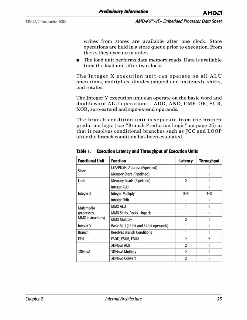
23542A/0—September 2000 AMD-K6™-2E+ Embedded Processor Data Sheet
Preliminary Information
writes from stores are available after one clock. Storeoperations are held in a store queue prior to execution. Fromthere, they execute in order.
■ The load unit performs data memory reads. Data is availablefrom the load unit after two clocks.
The Integer X execution unit can operate on all ALUoperations, multiplies, divides (signed and unsigned), shifts,and rotates.
The Integer Y execution unit can operate on the basic word anddoubleword ALU operations—ADD, AND, CMP, OR, SUB,XOR, zero-extend and sign-extend operands.
The branch condition unit is separate from the branchprediction logic (see “Branch-Prediction Logic” on page 25) inthat it resolves conditional branches such as JCC and LOOPafter the branch condition has been evaluated.
Table 1. Execution Latency and Throughput of Execution Units
Functional Unit Function Latency Throughput
StoreLEA/PUSH, Address (Pipelined) 1 1
Memory Store (Pipelined) 1 1
Load Memory Loads (Pipelined) 2 1
Integer X
Integer ALU 1 1
Integer Multiply 2–3 2–3
Integer Shift 1 1
Multimedia (processesMMX instructions)
MMX ALU 1 1
MMX Shifts, Packs, Unpack 1 1
MMX Multiply 2 1
Integer Y Basic ALU (16-bit and 32-bit operands) 1 1
Branch Resolves Branch Conditions 1 1
FPU FADD, FSUB, FMUL 2 2
3DNow!
3DNow! ALU 2 1
3DNow! Multiply 2 1
3DNow! Convert 2 1
Chapter 2 Internal Architecture 23
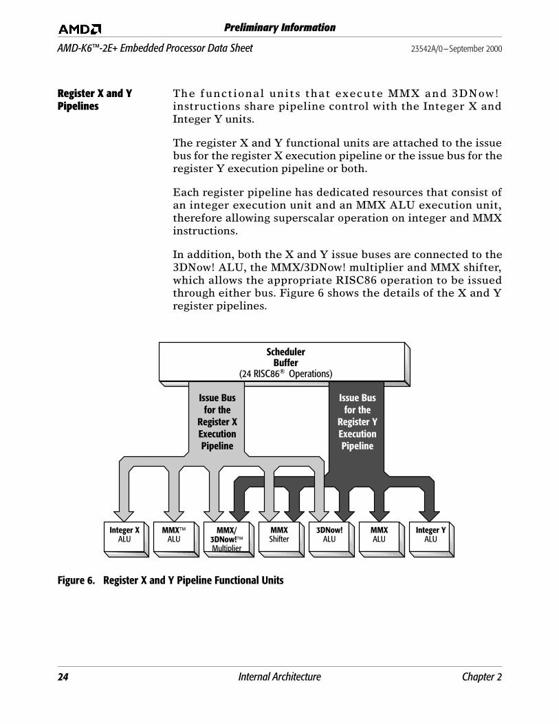
AMD-K6™-2E+ Embedded Processor Data Sheet 23542A/0—September 2000
Preliminary Information
Register X and Y Pipelines
The functional units that execute MMX and 3DNow!instructions share pipeline control with the Integer X andInteger Y units.
The register X and Y functional units are attached to the issuebus for the register X execution pipeline or the issue bus for theregister Y execution pipeline or both.
Each register pipeline has dedicated resources that consist ofan integer execution unit and an MMX ALU execution unit,therefore allowing superscalar operation on integer and MMXinstructions.
In addition, both the X and Y issue buses are connected to the3DNow! ALU, the MMX/3DNow! multiplier and MMX shifter,which allows the appropriate RISC86 operation to be issuedthrough either bus. Figure 6 shows the details of the X and Yregister pipelines.
Figure 6. Register X and Y Pipeline Functional Units
MMX/3DNow!ÉMultiplier
Integer XALU
MMXÉALU
MMXShifter
3DNow!ALU
MMXALU
Integer YALU
SchedulerBuffer
(24 RISC86® Operations)
Issue Busfor the
Register XExecutionPipeline
Issue Busfor the
Register YExecutionPipeline
24 Internal Architecture Chapter 2
23542A/0—September 2000 AMD-K6™-2E+ Embedded Processor Data Sheet
Preliminary Information
2.6 Branch-Prediction Logic
Sophisticated branch logic that can minimize or hide the impactof changes in program flow is designed into the AMD-K6-2E+processor. Branches in x86 code fit into two categories:
■ Unconditional branches always change program flow (that is,the branches are always taken)
■ Conditional branches may or may not divert program flow(that is, the branches are taken or not-taken). When aconditional branch is not taken, the processor simplycontinues decoding and executing the next instructions inmemory.
Typical applications have up to 10% of unconditional branchesand another 10% to 20% condit ional branches. TheAMD-K6-2E+ processor branch logic has been designed tohandle this type of program behavior and to minimize itsnegative effects on instruction execution, such as stalls due todelayed instruction fetching and the draining of the processorpipeline. The branch logic contains an 8192-entry branchhistory table, a 16-entry by 16-byte branch target cache, a16-entry return address stack, and a branch execution unit.
Branch History Table The AMD-K6-2E+ processor handles unconditional brancheswithout any penalty by redirecting instruction fetching to thetarget address of the unconditional branch. However,conditional branches require the use of the dynamicbranch-prediction mechanism built into the AMD-K6-2E+processor.
A two-level adaptive history algorithm is implemented in an8192-entry branch history table. This table stores executedbranch information, predicts individual branches, and predictsthe behavior of groups of branches.
To accommodate the large branch history table, theAMD-K6-2E+ processor does not store predicted targetaddresses. Instead, the branch target addresses are calculatedon-the-fly using ALUs during the decode stage. The adderscalculate all possible target addresses before the instructionsare fully decoded and the processor chooses which addressesare valid.
Chapter 2 Internal Architecture 25

AMD-K6™-2E+ Embedded Processor Data Sheet 23542A/0—September 2000
Preliminary Information
Branch Target Cache To avoid a one clock cache-fetch penalty when a branch ispredicted taken, a built-in branch target cache supplies the first16 bytes of instructions directly to the instruction buffer(assuming the target address hits this cache). (See Figure 3 onpage 18.)
The branch target cache is organized as 16 entries of 16 bytes.In total, the branch prediction logic achieves branch predictionrates greater than 95%.
Return Address Stack The return address stack is a special device designed tooptimize CALL and RET pairs. Software is typically compiledwith subroutines that are frequently called from various placesin a program. This is usually done to save space.
Entry into the subroutine occurs with the execution of a CALLinstruction. At that time, the processor pushes the address ofthe next instruction in memory following the CALL instructiononto the stack (allocated space in memory). When the processorencounters a RET instruction (within or at the end of thesubroutine), the branch logic pops the address from the stackand begins fetching from that location. To avoid the latency ofmain memory accesses during CALL and RET operations, thereturn address stack caches the pushed addresses.
Branch Execution Unit
The branch execution unit enables efficient speculativeexecution. This unit gives the processor the ability to executeinstructions beyond conditional branches before knowingwhether the branch prediction was correct.
The AMD-K6-2E+ processor does not permanently update thex86 registers or memory locations until all speculativelyexecuted conditional branch instructions are resolved. When aprediction is incorrect, the processor backs out to the point ofthe mispredicted branch instruction and restores all registers.The AMD-K6-2E+ processor can support up to sevenoutstanding branches.
26 Internal Architecture Chapter 2
23542A/0—September 2000 AMD-K6™-2E+ Embedded Processor Data Sheet
Preliminary Information
3 Software Environment
This chapter provides a general overview of the AMD-K6-2E+processor’s x86 software environment and briefly describes thedata types, registers, operating modes, interrupts, andinstructions supported by the AMD-K6-2E+ processorarchitecture and design implementation.
The AMD-K6-2E+ processor implements the same ten Model-Specific Registers (MSRs) as the AMD-K6-2 and AMD-K6-2Eprocessors Model 8/[F:8], and the bits and fields within theseten MSRs are defined identically. The AMD-K6-2E+ processorsupports an additional MSR for cache control. The low-powerversions of the AMD-K6-2E+ processor support a twelfth MSRto control the AMD PowerNow! technology functions.
See “Model-Specific Registers (MSR)” on page 44 for the MSRdefinitions.
The model number for the AMD-K6-2E+ processor is ModelD/[7:4], where the actual stepping can be any value in the range[7:4].
3.1 Registers
The AMD-K6-2E+ processor contains all the registers definedby the x86 architecture, including general-purpose, segment,floating-point, MMX/3DNow!, EFLAGS, control, task, debug,test, and descriptor/memory-management registers.
In addition, this chapter provides information on theAMD-K6-2E+ processor MSRs.
Note: Areas of the register designated as Reserved should not bemodified by software.
Chapter 3 Software Environment 27
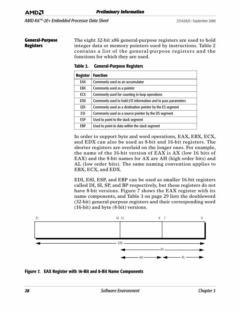
AMD-K6™-2E+ Embedded Processor Data Sheet 23542A/0—September 2000
Preliminary Information
General-Purpose Registers
The eight 32-bit x86 general-purpose registers are used to holdinteger data or memory pointers used by instructions. Table 2contains a list of the general-purpose registers and thefunctions for which they are used.
In order to support byte and word operations, EAX, EBX, ECX,and EDX can also be used as 8-bit and 16-bit registers. Theshorter registers are overlaid on the longer ones. For example,the name of the 16-bit version of EAX is AX (low 16 bits ofEAX) and the 8-bit names for AX are AH (high order bits) andAL (low order bits). The same naming convention applies toEBX, ECX, and EDX.
EDI, ESI, ESP, and EBP can be used as smaller 16-bit registerscalled DI, SI, SP, and BP respectively, but these registers do nothave 8-bit versions. Figure 7 shows the EAX register with itsname components, and Table 3 on page 29 lists the doubleword(32-bit) general-purpose registers and their corresponding word(16-bit) and byte (8-bit) versions.
Figure 7. EAX Register with 16-Bit and 8-Bit Name Components
Table 2. General-Purpose Registers
Register FunctionEAX Commonly used as an accumulator
EBX Commonly used as a pointer
ECX Commonly used for counting in loop operations
EDX Commonly used to hold I/O information and to pass parameters
EDI Commonly used as a destination pointer by the ES segment
ESI Commonly used as a source pointer by the DS segment
ESP Used to point to the stack segment
EBP Used to point to data within the stack segment
8 7 0151631
EAX
AX
AH AL
28 Software Environment Chapter 3
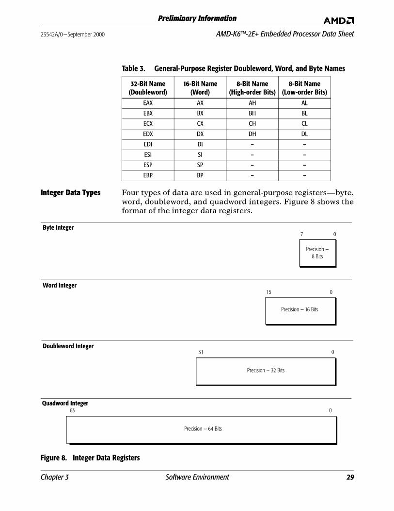
23542A/0—September 2000 AMD-K6™-2E+ Embedded Processor Data Sheet
Preliminary Information
Integer Data Types Four types of data are used in general-purpose registers—byte,word, doubleword, and quadword integers. Figure 8 shows theformat of the integer data registers.
Figure 8. Integer Data Registers
Table 3. General-Purpose Register Doubleword, Word, and Byte Names
32-Bit Name (Doubleword)
16-Bit Name (Word)
8-Bit Name(High-order Bits)
8-Bit Name (Low-order Bits)
EAX AX AH AL
EBX BX BH BL
ECX CX CH CL
EDX DX DH DL
EDI DI – –
ESI SI – –
ESP SP – –
EBP BP – –
15 0
31 0
Precision — 32 Bits
Precision — 16 Bits
Word Integer
Doubleword Integer
7 0
Precision — 8 Bits
Byte Integer
63 0
Precision — 64 Bits
Quadword Integer
Chapter 3 Software Environment 29

AMD-K6™-2E+ Embedded Processor Data Sheet 23542A/0—September 2000
Preliminary Information
Segment Registers The six 16-bit segment registers are used as pointers to areas(segments) of memory. Table 4 lists the segment registers andtheir functions. Figure 9 shows the format for all six segmentregisters.
Figure 9. Segment Register
Segment Usage The operating system determines the type of memory modelthat is implemented. The segment register usage is determinedby the operating system’s memory model. In a real modememory model, the segment register points to the base addressin memory.
In a protected mode memory model the segment register iscalled a selector and it selects a segment descriptor in adescriptor table. This descriptor contains a pointer to the baseof the segment, the limit of the segment, and various protectionattributes. For more information on descriptor formats, see“Descriptors and Gates” on page 59. Figure 10 on page 31 showssegment usage for Real mode and Protected mode memorymodels.
Table 4. Segment Registers
SegmentRegister Segment Register Function
CS Code segment, where instructions are located
DS Data segment, where data is located
ES Data segment, where data is located
FS Data segment, where data is located
GS Data segment, where data is located
SS Stack segment
015
30 Software Environment Chapter 3
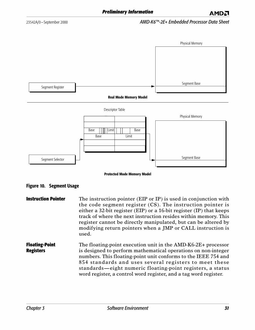
23542A/0—September 2000 AMD-K6™-2E+ Embedded Processor Data Sheet
Preliminary Information
Figure 10. Segment Usage
Instruction Pointer The instruction pointer (EIP or IP) is used in conjunction withthe code segment register (CS). The instruction pointer iseither a 32-bit register (EIP) or a 16-bit register (IP) that keepstrack of where the next instruction resides within memory. Thisregister cannot be directly manipulated, but can be altered bymodifying return pointers when a JMP or CALL instruction isused.
Floating-Point Registers
The floating-point execution unit in the AMD-K6-2E+ processoris designed to perform mathematical operations on non-integernumbers. This floating-point unit conforms to the IEEE 754 and854 standards and uses several registers to meet thesestandards—eight numeric floating-point registers, a statusword register, a control word register, and a tag word register.
Segment Register
Real Mode Memory Model
Segment Selector
Physical Memory
Protected Mode Memory Model
Base
Descriptor Table
Physical Memory
Segment Base
Base
Limit
BaseLimit
Segment Base
Chapter 3 Software Environment 31
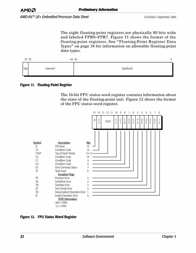
AMD-K6™-2E+ Embedded Processor Data Sheet 23542A/0—September 2000
Preliminary Information
The eight floating-point registers are physically 80 bits wideand labeled FPR0–FPR7. Figure 11 shows the format of thefloating-point registers. See “Floating-Point Register DataTypes” on page 34 for information on allowable floating-pointdata types.
Figure 11. Floating-Point Register
The 16-bit FPU status word register contains information aboutthe state of the floating-point unit. Figure 12 shows the formatof the FPU status word register.
Figure 12. FPU Status Word Register
64 63 07879
Sign Exponent Significand
9 8 7 6 5 4 3 2 1 0101112131415
PE
OE
ES
C0
C1
IE
ZE
UE
SFTOSPC
3B C
2DE
Symbol Description BitsB FPU Busy 15C3 Condition Code 14TOSP Top of Stack Pointer 13–11C2 Condition Code 10C1 Condition Code 9C0 Condition Code 8ES Error Summary Status 7SF Stack Fault 6
Exception FlagsPE Precision Error 5UE Underflow Error 4OE Overflow Error 3ZE Zero Divide Error 2DE Denormalized Operation Error 1IE Invalid Operation Error 0
TOSP Information000 = FPR0111 = FPR7
32 Software Environment Chapter 3
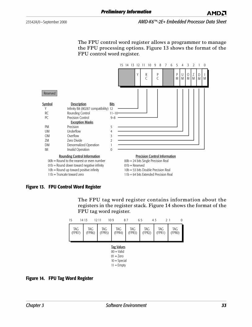
23542A/0—September 2000 AMD-K6™-2E+ Embedded Processor Data Sheet
Preliminary Information
The FPU control word register allows a programmer to managethe FPU processing options. Figure 13 shows the format of theFPU control word register.
Figure 13. FPU Control Word Register
The FPU tag word register contains information about theregisters in the register stack. Figure 14 shows the format of theFPU tag word register.
Figure 14. FPU Tag Word Register
9 8 7 6 5 4 3 2 1 0101112131415
PM
OM
PC
RC
IM
ZM
UM
DM
Rounding Control Information00b = Round to the nearest or even number01b = Round down toward negative infinity10b = Round up toward positive infinity11b = Truncate toward zero
Y
Precision Control Information00b = 24 bits Single Precision Real01b = Reserved10b = 53 bits Double Precision Real11b = 64 bits Extended Precision Real
Reserved
Symbol Description BitsY Infinity Bit (80287 compatibility) 12RC Rounding Control 11–10PC Precision Control 9–8
Exception MasksPM Precision 5UM Underflow 4OM Overflow 3ZM Zero Divide 2DM Denormalized Operation 1IM Invalid Operation 0
Tag Values00 = Valid01 = Zero10 = Special11 = Empty
8 7 6 5 4 3 2 1 0101112131415
TAG(FPR7)
TAG(FPR6)
TAG(FPR4)
TAG(FPR5)
TAG(FPR2)
TAG(FPR3)
TAG(FPR0)
TAG(FPR1)
9
Chapter 3 Software Environment 33

AMD-K6™-2E+ Embedded Processor Data Sheet 23542A/0—September 2000
Preliminary Information
Floating-Point Register Data Types
Floating-point registers use four different types of data—packed decimal, single-precision real, double-precision real,and extended-precision real. Figures 15 and 16 show theformats for these registers.
Figure 15. Packed Decimal Data Register
Figure 16. Precision Real Data Registers
079
Precision — 18 Digits, 72 Bits Used, 4-Bits/Digit
71
SIgnore
or Zero
78 72
Description BitsIgnored on Load, Zeros on Store 78-72Sign Bit 79
063Double-Precision Real
31 0Single-Precision Real
079
22
S Biased Exponent
78
23
SBiased
Exponent
6364
5152
Biased Exponent
S
Significand
Significand
Significand
30
62
Extended-Precision Real
S = Sign Bit
S = Sign Bit
S = Sign Bit
I
62
I = Integer Bit
34 Software Environment Chapter 3
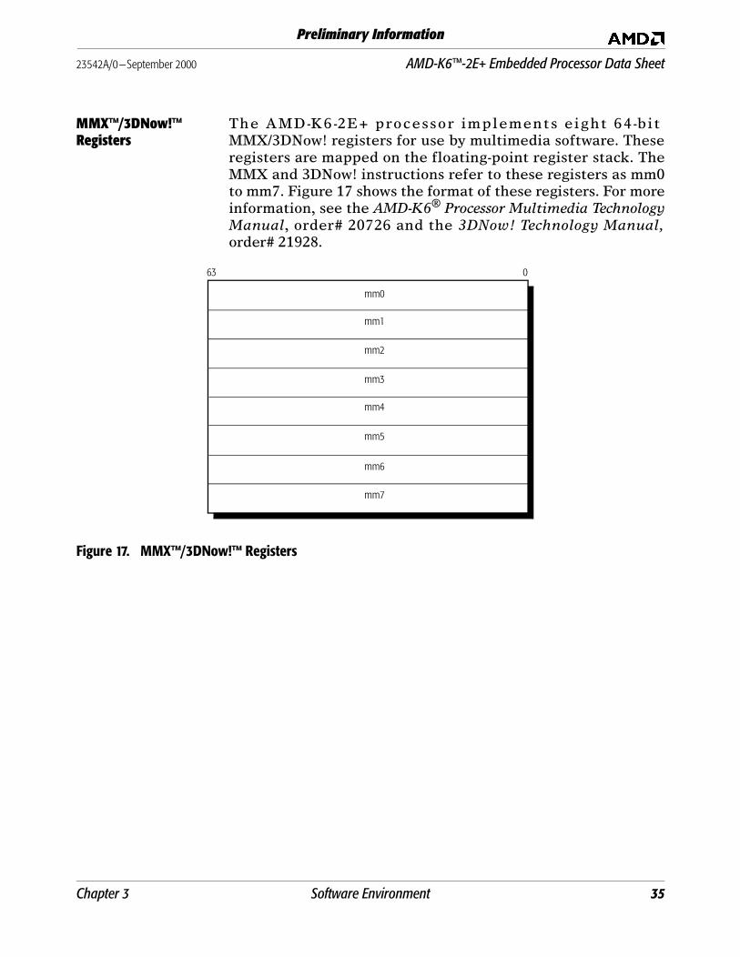
23542A/0—September 2000 AMD-K6™-2E+ Embedded Processor Data Sheet
Preliminary Information
MMX™/3DNow!™ Registers
The AMD-K6-2E+ processor implements eight 64-bitMMX/3DNow! registers for use by multimedia software. Theseregisters are mapped on the floating-point register stack. TheMMX and 3DNow! instructions refer to these registers as mm0to mm7. Figure 17 shows the format of these registers. For moreinformation, see the AMD-K6® Processor Multimedia TechnologyManual, order# 20726 and the 3DNow! Technology Manual,order# 21928.
Figure 17. MMX™/3DNow!™ Registers
63 0
mm0
mm7
mm1
mm6
mm5
mm2
mm3
mm4
Chapter 3 Software Environment 35
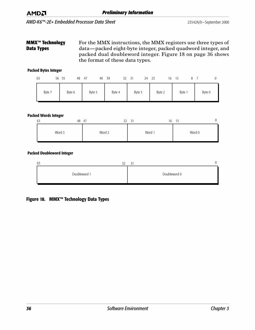
AMD-K6™-2E+ Embedded Processor Data Sheet 23542A/0—September 2000
Preliminary Information
MMX™ Technology Data Types
For the MMX instructions, the MMX registers use three types ofdata—packed eight-byte integer, packed quadword integer, andpacked dual doubleword integer. Figure 18 on page 36 showsthe format of these data types.
Figure 18. MMX™ Technology Data Types
63 0
Packed Bytes Integer
63 0Packed Words Integer
63 0
Packed Doubleword Integer
32 31
48 47 32 31 16 15
56 55 48 47 40 39 32 31 24 23 16 15 8 7
Byte 7 Byte 6 Byte 5 Byte 4 Byte 3 Byte 2 Byte 1 Byte 0
Word 0Word 1Word 2Word 3
Doubleword 1 Doubleword 0
36 Software Environment Chapter 3
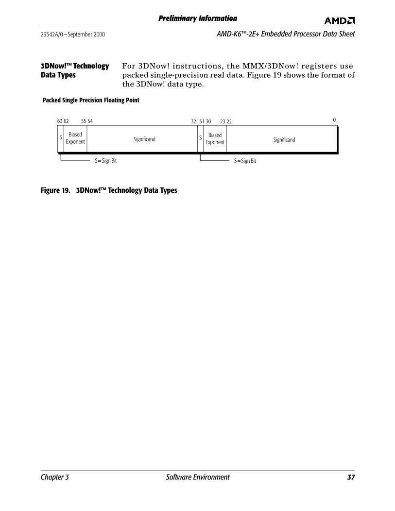
23542A/0—September 2000 AMD-K6™-2E+ Embedded Processor Data Sheet
Preliminary Information
3DNow!™ Technology Data Types
For 3DNow! instructions, the MMX/3DNow! registers usepacked single-precision real data. Figure 19 shows the format ofthe 3DNow! data type.
Figure 19. 3DNow!™ Technology Data Types
63 62 032 31 30
Packed Single Precision Floating Point
55 54 23 22
Biased Exponent
S Significand
S = Sign Bit
Biased Exponent
S Significand
S = Sign Bit
Chapter 3 Software Environment 37
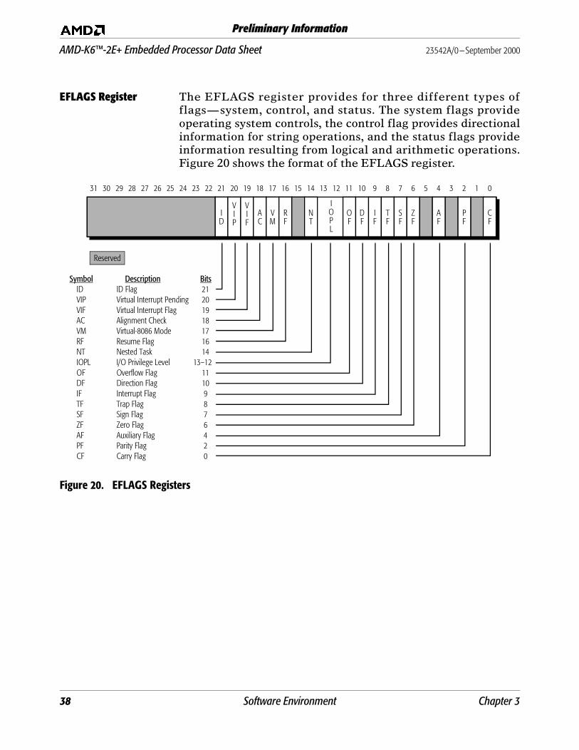
AMD-K6™-2E+ Embedded Processor Data Sheet 23542A/0—September 2000
Preliminary Information
EFLAGS Register The EFLAGS register provides for three different types offlags—system, control, and status. The system flags provideoperating system controls, the control flag provides directionalinformation for string operations, and the status flags provideinformation resulting from logical and arithmetic operations.Figure 20 shows the format of the EFLAGS register.
Figure 20. EFLAGS Registers
9 8 7 6 5 4 3 2 1 0101112131415161718192021
IOPL
31 30 29 28 27 26 25 24 23 22
AF
PF
ZF
SF
IF
DF
TF
OF
NT
RF
VM
AC
VIF
VIP
ID
CF
Reserved
Symbol Description BitsID ID Flag 21VIP Virtual Interrupt Pending 20VIF Virtual Interrupt Flag 19AC Alignment Check 18VM Virtual-8086 Mode 17RF Resume Flag 16NT Nested Task 14IOPL I/O Privilege Level 13–12OF Overflow Flag 11DF Direction Flag 10IF Interrupt Flag 9TF Trap Flag 8SF Sign Flag 7ZF Zero Flag 6AF Auxiliary Flag 4PF Parity Flag 2CF Carry Flag 0
38 Software Environment Chapter 3

23542A/0—September 2000 AMD-K6™-2E+ Embedded Processor Data Sheet
Preliminary Information
Control Registers The five control registers contain system control bits andpointers. Figures 21 through 25 show the formats of the controlregisters.
Figure 21. Control Register 4 (CR4)
Figure 22. Control Register 3 (CR3)
Figure 23. Control Register 2 (CR2)
7 6 5 4 3 2 1 031
PSE
TSD
MCE
VME
DE
PVI
Reserved
Symbol Description BitMCE Machine Check Enable 6PSE Page Size Extensions 4DE Debugging Extensions 3TSD Time Stamp Disable 2PVI Protected Virtual Interrupts 1VME Virtual-8086 Mode Extensions 0
PCD
9 8 7 6 5 4 3 2 1 010111213141516171819202131 30 29 28 27 26 25 24 23 22
Page Directory BasePWT
Reserved
Symbol Description BitPCD Page Cache Disable 4PWT Page Writethrough 3
031
Page Fault Linear Address
Chapter 3 Software Environment 39
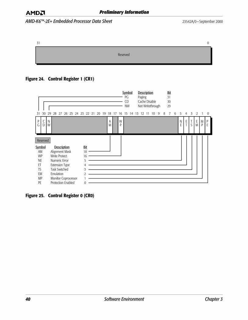
AMD-K6™-2E+ Embedded Processor Data Sheet 23542A/0—September 2000
Preliminary Information
Figure 24. Control Register 1 (CR1)
Figure 25. Control Register 0 (CR0)
031
Reserved
ET
TS
9 8 7 6 5 4 3 2 1 010111213141516171819202131 30 29 28 27 26 25 24 23 22
AM
EM
WP
MP
PE
NE
PG
CD
NW
Reserved
Symbol Description BitAM Alignment Mask 18WP Write Protect 16NE Numeric Error 5ET Extension Type 4TS Task Switched 3EM Emulation 2MP Monitor Coprocessor 1PE Protection Enabled 0
Symbol Description BitPG Paging 31CD Cache Disable 30NW Not Writethrough 29
40 Software Environment Chapter 3
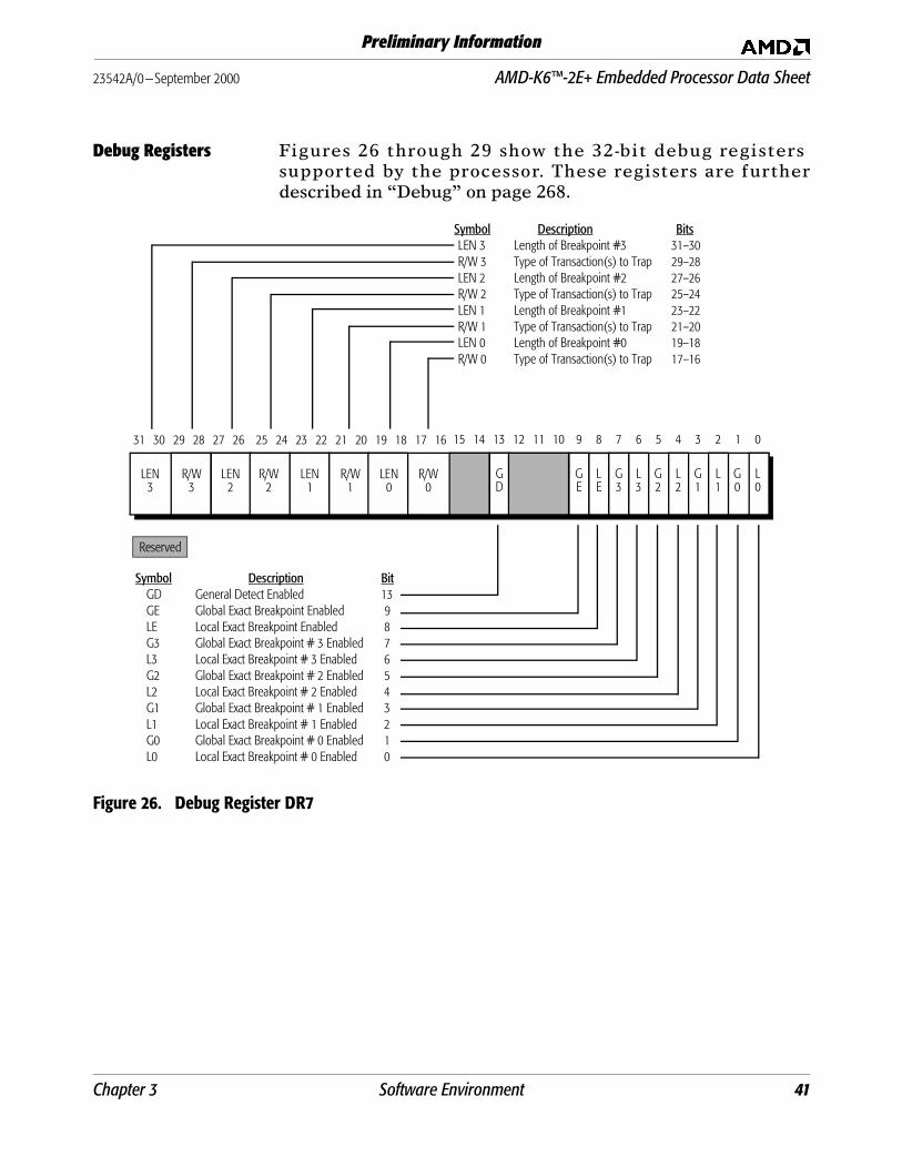
23542A/0—September 2000 AMD-K6™-2E+ Embedded Processor Data Sheet
Preliminary Information
Debug Registers Figures 26 through 29 show the 32-bit debug registerssupported by the processor. These registers are furtherdescribed in “Debug” on page 268.
Figure 26. Debug Register DR7
9 8 7 6 5 4 3 2 1 0101112131415
L2
L1
L3
G3
GE
LE
L0
G0
G1
G2
GD
25 24 23 22 21 20 19 18 17 16262728293031
R/W 3
LEN 3
R/W 2
LEN 2
R/W 1
LEN 1
R/W 0
LEN 0
Reserved
Symbol Description BitGD General Detect Enabled 13GE Global Exact Breakpoint Enabled 9LE Local Exact Breakpoint Enabled 8G3 Global Exact Breakpoint # 3 Enabled 7L3 Local Exact Breakpoint # 3 Enabled 6G2 Global Exact Breakpoint # 2 Enabled 5L2 Local Exact Breakpoint # 2 Enabled 4G1 Global Exact Breakpoint # 1 Enabled 3L1 Local Exact Breakpoint # 1 Enabled 2G0 Global Exact Breakpoint # 0 Enabled 1L0 Local Exact Breakpoint # 0 Enabled 0
Symbol Description BitsLEN 3 Length of Breakpoint #3 31–30R/W 3 Type of Transaction(s) to Trap 29–28LEN 2 Length of Breakpoint #2 27–26R/W 2 Type of Transaction(s) to Trap 25–24LEN 1 Length of Breakpoint #1 23–22R/W 1 Type of Transaction(s) to Trap 21–20LEN 0 Length of Breakpoint #0 19–18R/W 0 Type of Transaction(s) to Trap 17–16
Chapter 3 Software Environment 41
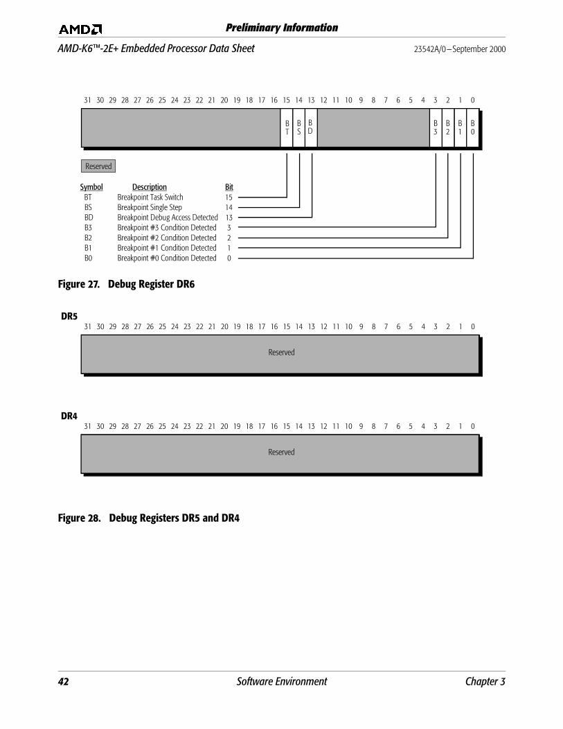
AMD-K6™-2E+ Embedded Processor Data Sheet 23542A/0—September 2000
Preliminary Information
Figure 27. Debug Register DR6
Figure 28. Debug Registers DR5 and DR4
9 8 7 6 5 4 3 2 1 010111213141516171819202131 30 29 28 27 26 25 24 23 22
B1
B2
BS
B0
BT
BD
B3
Reserved
Symbol Description BitBT Breakpoint Task Switch 15 BS Breakpoint Single Step 14 BD Breakpoint Debug Access Detected 13 B3 Breakpoint #3 Condition Detected 3 B2 Breakpoint #2 Condition Detected 2 B1 Breakpoint #1 Condition Detected 1 B0 Breakpoint #0 Condition Detected 0
9 8 7 6 5 4 3 2 1 010111213141516171819202131 30 29 28 27 26 25 24 23 22
Reserved
DR5
9 8 7 6 5 4 3 2 1 010111213141516171819202131 30 29 28 27 26 25 24 23 22
Reserved
DR4
42 Software Environment Chapter 3

23542A/0—September 2000 AMD-K6™-2E+ Embedded Processor Data Sheet
Preliminary Information
Figure 29. Debug Registers DR3, DR2, DR1, and DR0
9 8 7 6 5 4 3 2 1 010111213141516171819202131 30 29 28 27 26 25 24 23 22
Breakpoint 3 32-bit Linear Address
DR3
9 8 7 6 5 4 3 2 1 010111213141516171819202131 30 29 28 27 26 25 24 23 22
Breakpoint 0 32-bit Linear Address
DR0
9 8 7 6 5 4 3 2 1 010111213141516171819202131 30 29 28 27 26 25 24 23 22
Breakpoint 2 32-bit Linear Address
DR2
9 8 7 6 5 4 3 2 1 010111213141516171819202131 30 29 28 27 26 25 24 23 22
Breakpoint 1 32-bit Linear Address
DR1
Chapter 3 Software Environment 43
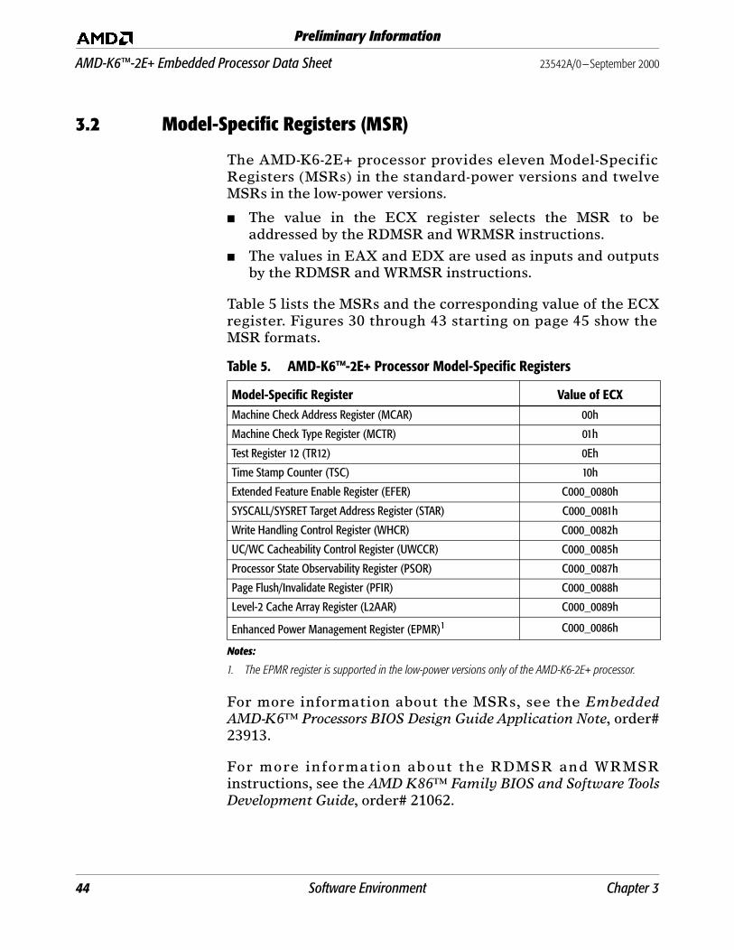
AMD-K6™-2E+ Embedded Processor Data Sheet 23542A/0—September 2000
Preliminary Information
3.2 Model-Specific Registers (MSR)
The AMD-K6-2E+ processor provides eleven Model-SpecificRegisters (MSRs) in the standard-power versions and twelveMSRs in the low-power versions.
■ The value in the ECX register selects the MSR to beaddressed by the RDMSR and WRMSR instructions.
■ The values in EAX and EDX are used as inputs and outputsby the RDMSR and WRMSR instructions.
Table 5 lists the MSRs and the corresponding value of the ECXregister. Figures 30 through 43 starting on page 45 show theMSR formats.
For more information about the MSRs, see the EmbeddedAMD-K6™ Processors BIOS Design Guide Application Note, order#23913.
For more information about the RDMSR and WRMSRinstructions, see the AMD K86™ Family BIOS and Software ToolsDevelopment Guide, order# 21062.
Table 5. AMD-K6™-2E+ Processor Model-Specific Registers
Model-Specific Register Value of ECXMachine Check Address Register (MCAR) 00h
Machine Check Type Register (MCTR) 01h
Test Register 12 (TR12) 0Eh
Time Stamp Counter (TSC) 10h
Extended Feature Enable Register (EFER) C000_0080h
SYSCALL/SYSRET Target Address Register (STAR) C000_0081h
Write Handling Control Register (WHCR) C000_0082h
UC/WC Cacheability Control Register (UWCCR) C000_0085h
Processor State Observability Register (PSOR) C000_0087h
Page Flush/Invalidate Register (PFIR) C000_0088h
Level-2 Cache Array Register (L2AAR) C000_0089h
Enhanced Power Management Register (EPMR)1
Notes:
1. The EPMR register is supported in the low-power versions only of the AMD-K6-2E+ processor.
C000_0086h
44 Software Environment Chapter 3
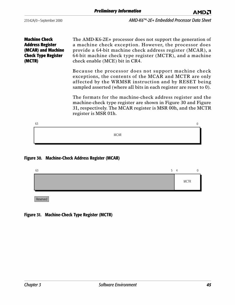
23542A/0—September 2000 AMD-K6™-2E+ Embedded Processor Data Sheet
Preliminary Information
Machine Check Address Register (MCAR) and Machine Check Type Register (MCTR)
The AMD-K6-2E+ processor does not support the generation ofa machine check exception. However, the processor doesprovide a 64-bit machine check address register (MCAR), a64-bit machine check type register (MCTR), and a machinecheck enable (MCE) bit in CR4.
Because the processor does not support machine checkexceptions, the contents of the MCAR and MCTR are onlyaffected by the WRMSR instruction and by RESET beingsampled asserted (where all bits in each register are reset to 0).
The formats for the machine-check address register and themachine-check type register are shown in Figure 30 and Figure31, respectively. The MCAR register is MSR 00h, and the MCTRregister is MSR 01h.
Figure 30. Machine-Check Address Register (MCAR)
Figure 31. Machine-Check Type Register (MCTR)
063
MCAR
5 4 063
MCTR
Reserved
Chapter 3 Software Environment 45

AMD-K6™-2E+ Embedded Processor Data Sheet 23542A/0—September 2000
Preliminary Information
Test Register 12 (TR12)
Test register 12 provides a method for disabling the L1 caches.Figure 32 shows the format of TR12. The TR12 register is MSR0Eh.
Figure 32. Test Register 12 (TR12)
Time Stamp Counter With each processor clock cycle, the processor increments the64-bit time stamp counter (TSC) MSR. Figure 33 shows theformat of the TSC. The TSC register is MSR 10h.
The counter can be written or read using the WRMSR orRDMSR instructions when the ECX register contains the value10h and CPL = 0. The counter can also be read using the RDTSCinstruction, but the procedure must be executing at privilegelevel 0 for the RDTSC instruction to execute. This condition isreflected by the status of the Time Stamp Disable (TSD) bit inCR4.
With either of these instructions, the EDX and EAX registershold the upper and lower dwords of the 64-bit value to bewritten to or read from the TSC, as follows:
■ EDX—Upper 32 bits of TSC
■ EAX—Lower 32 bits of TSC
The TSC can be loaded with any arbitrary value. This feature iscompatible with the Pentium processor.
Figure 33. Time Stamp Counter (TSC)
4 2 1 063
CI
3
ReservedSymbol Description Bit
CI Cache Inhibit Bit 3
063
TSC
46 Software Environment Chapter 3
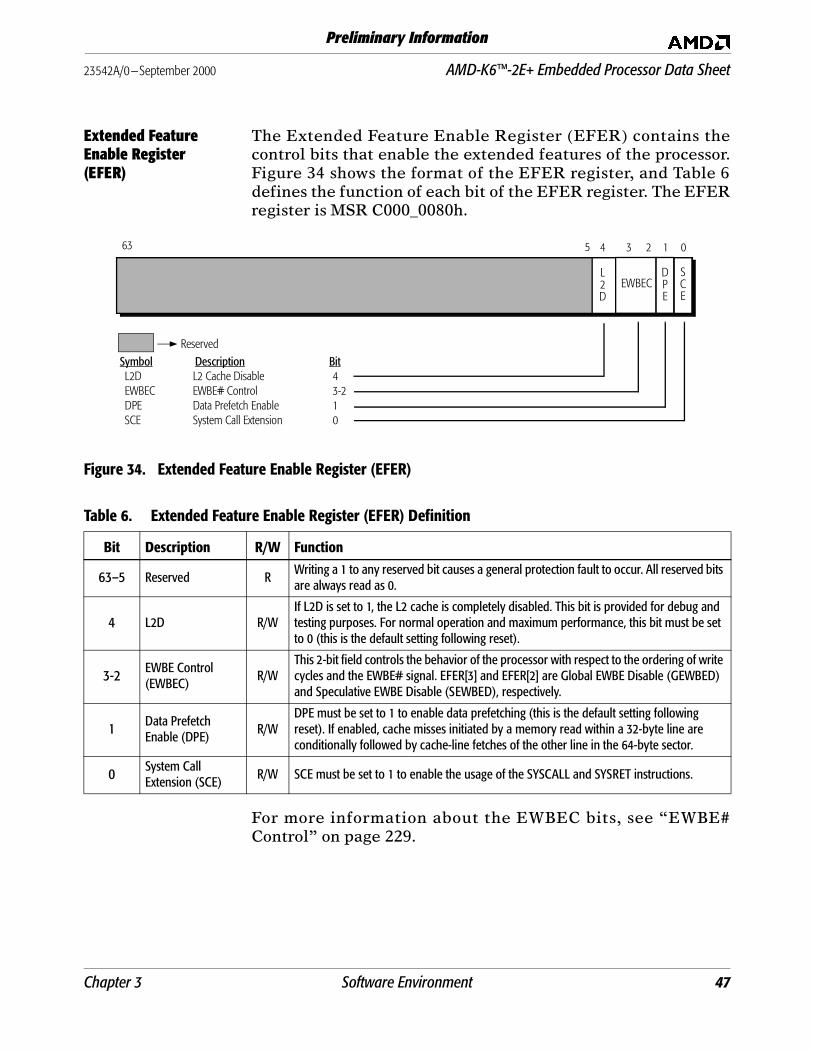
23542A/0—September 2000 AMD-K6™-2E+ Embedded Processor Data Sheet
Preliminary Information
Extended Feature Enable Register (EFER)
The Extended Feature Enable Register (EFER) contains thecontrol bits that enable the extended features of the processor.Figure 34 shows the format of the EFER register, and Table 6defines the function of each bit of the EFER register. The EFERregister is MSR C000_0080h.
Figure 34. Extended Feature Enable Register (EFER)
For more information about the EWBEC bits, see “EWBE#Control” on page 229.
Table 6. Extended Feature Enable Register (EFER) Definition
Bit Description R/W Function
63–5 Reserved RWriting a 1 to any reserved bit causes a general protection fault to occur. All reserved bits are always read as 0.
4 L2D R/WIf L2D is set to 1, the L2 cache is completely disabled. This bit is provided for debug and testing purposes. For normal operation and maximum performance, this bit must be set to 0 (this is the default setting following reset).
3-2 EWBE Control (EWBEC)
R/WThis 2-bit field controls the behavior of the processor with respect to the ordering of write cycles and the EWBE# signal. EFER[3] and EFER[2] are Global EWBE Disable (GEWBED) and Speculative EWBE Disable (SEWBED), respectively.
1 Data Prefetch Enable (DPE)
R/WDPE must be set to 1 to enable data prefetching (this is the default setting following reset). If enabled, cache misses initiated by a memory read within a 32-byte line are conditionally followed by cache-line fetches of the other line in the 64-byte sector.
0 System Call Extension (SCE)
R/W SCE must be set to 1 to enable the usage of the SYSCALL and SYSRET instructions.
1 063
SCE
Reserved
234
DPE
EWBEC
Symbol Description BitL2D L2 Cache Disable 4EWBEC EWBE# Control 3-2DPE Data Prefetch Enable 1SCE System Call Extension 0
5
L2D
Chapter 3 Software Environment 47
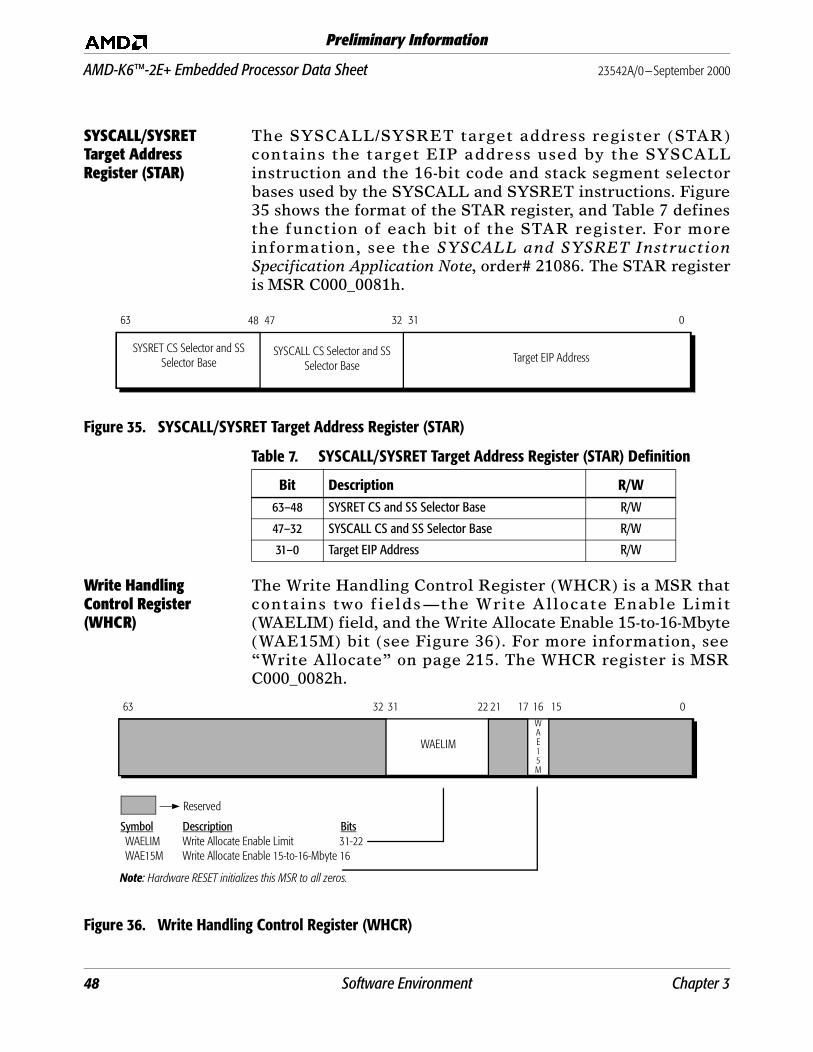
AMD-K6™-2E+ Embedded Processor Data Sheet 23542A/0—September 2000
Preliminary Information
SYSCALL/SYSRET Target Address Register (STAR)
The SYSCALL/SYSRET target address register (STAR)contains the target EIP address used by the SYSCALLinstruction and the 16-bit code and stack segment selectorbases used by the SYSCALL and SYSRET instructions. Figure35 shows the format of the STAR register, and Table 7 definesthe function of each bit of the STAR register. For moreinformation, see the SYSCALL and SYSRET InstructionSpecification Application Note, order# 21086. The STAR registeris MSR C000_0081h.
Figure 35. SYSCALL/SYSRET Target Address Register (STAR)
Write Handling Control Register (WHCR)
The Write Handling Control Register (WHCR) is a MSR thatcontains two fields —the Write Allocate Enable Limit(WAELIM) field, and the Write Allocate Enable 15-to-16-Mbyte(WAE15M) bit (see Figure 36). For more information, see“Write Allocate” on page 215. The WHCR register is MSRC000_0082h.
Figure 36. Write Handling Control Register (WHCR)
31 063
Target EIP Address
324748
SYSCALL CS Selector and SS Selector Base
SYSRET CS Selector and SS Selector Base
Table 7. SYSCALL/SYSRET Target Address Register (STAR) Definition
Bit Description R/W63–48 SYSRET CS and SS Selector Base R/W
47–32 SYSCALL CS and SS Selector Base R/W
31–0 Target EIP Address R/W
1522 063
Reserved
WAELIM
16
Note: Hardware RESET initializes this MSR to all zeros.
WAE15M
Symbol Description BitsWAELIM Write Allocate Enable Limit 31-22WAE15M Write Allocate Enable 15-to-16-Mbyte 16
17213132
48 Software Environment Chapter 3
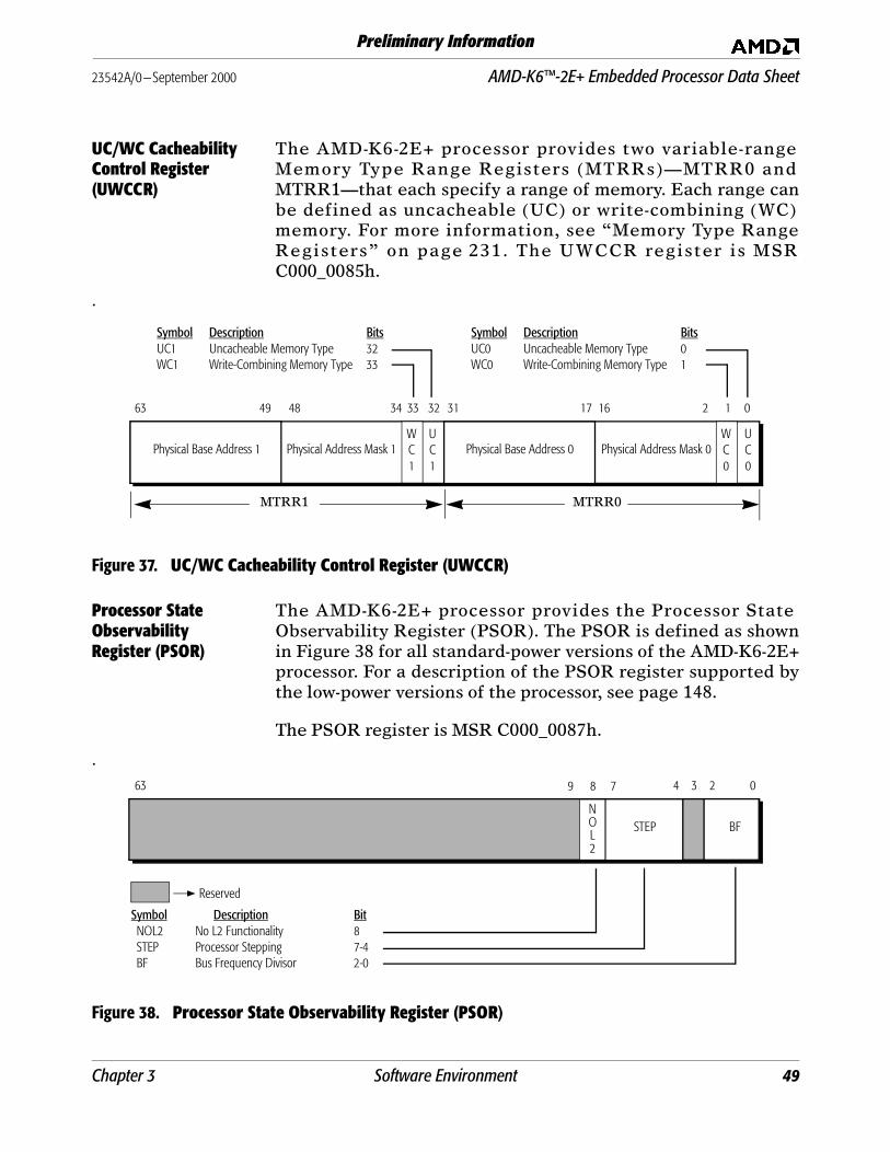
23542A/0—September 2000 AMD-K6™-2E+ Embedded Processor Data Sheet
Preliminary Information
UC/WC Cacheability Control Register (UWCCR)
The AMD-K6-2E+ processor provides two variable-rangeMemory Type Range Registers (MTRRs)—MTRR0 andMTRR1—that each specify a range of memory. Each range canbe defined as uncacheable (UC) or write-combining (WC)memory. For more information, see “Memory Type RangeRegisters” on page 231. The UWCCR register is MSRC000_0085h.
.
Figure 37. UC/WC Cacheability Control Register (UWCCR)
Processor State Observability Register (PSOR)
The AMD-K6-2E+ processor provides the Processor StateObservability Register (PSOR). The PSOR is defined as shownin Figure 38 for all standard-power versions of the AMD-K6-2E+processor. For a description of the PSOR register supported bythe low-power versions of the processor, see page 148.
The PSOR register is MSR C000_0087h.
.
Figure 38. Processor State Observability Register (PSOR)
16 063
Physical Address Mask 0
1731
Physical Base Address 0
12
Physical Address Mask 1Physical Base Address 1
3233344849
UC0
WC0
UC1
WC1
MTRR1 MTRR0
Symbol Description BitsUC0 Uncacheable Memory Type 0WC0 Write-Combining Memory Type 1
Symbol Description BitsUC1 Uncacheable Memory Type 32WC1 Write-Combining Memory Type 33
2 063
BF
Reserved
Symbol Description BitNOL2 No L2 Functionality 8STEP Processor Stepping 7-4BF Bus Frequency Divisor 2-0
34
STEP
789
NOL2
Chapter 3 Software Environment 49
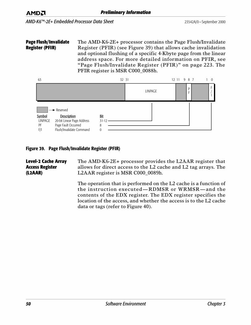
AMD-K6™-2E+ Embedded Processor Data Sheet 23542A/0—September 2000
Preliminary Information
Page Flush/Invalidate Register (PFIR)
The AMD-K6-2E+ processor contains the Page Flush/InvalidateRegister (PFIR) (see Figure 39) that allows cache invalidationand optional flushing of a specific 4-Kbyte page from the linearaddress space. For more detailed information on PFIR, see“Page Flush/Invalidate Register (PFIR)” on page 223. ThePFIR register is MSR C000_0088h.
Figure 39. Page Flush/Invalidate Register (PFIR)
Level-2 Cache Array Access Register (L2AAR)
The AMD-K6-2E+ processor provides the L2AAR register thatallows for direct access to the L2 cache and L2 tag arrays. TheL2AAR register is MSR C000_0089h.
The operation that is performed on the L2 cache is a function ofthe instruction executed— RDMSR or WRMSR — and thecontents of the EDX register. The EDX register specifies thelocation of the access, and whether the access is to the L2 cachedata or tags (refer to Figure 40).
LINPAGE
1 063
F/I
Reserved
Symbol Description BitLINPAGE 20-bit Linear Page Address 31-12PF Page Fault Occurred 8F/I Flush/Invalidate Command 0
1131 1232
PF
9 8 7
50 Software Environment Chapter 3
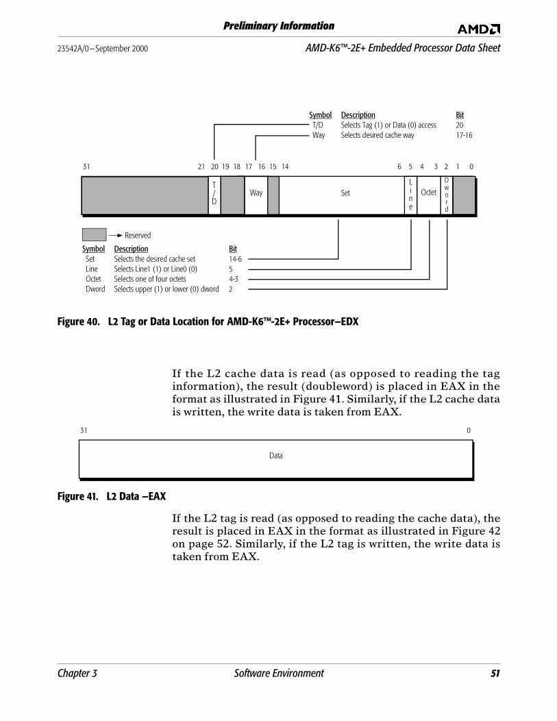
23542A/0—September 2000 AMD-K6™-2E+ Embedded Processor Data Sheet
Preliminary Information
Figure 40. L2 Tag or Data Location for AMD-K6™-2E+ Processor—EDX
If the L2 cache data is read (as opposed to reading the taginformation), the result (doubleword) is placed in EAX in theformat as illustrated in Figure 41. Similarly, if the L2 cache datais written, the write data is taken from EAX.
Figure 41. L2 Data —EAX
If the L2 tag is read (as opposed to reading the cache data), theresult is placed in EAX in the format as illustrated in Figure 42on page 52. Similarly, if the L2 tag is written, the write data istaken from EAX.
Reserved
0
Set
2131 20 19 17 16 51518
Way
4 3 2 16
Symbol Description BitSet Selects the desired cache set 14-6Line Selects Line1 (1) or Line0 (0) 5Octet Selects one of four octets 4-3Dword Selects upper (1) or lower (0) dword 2
Line
Octet
Dword
T/D
Symbol Description BitT/D Selects Tag (1) or Data (0) access 20Way Selects desired cache way 17-16
14
031
Data
Chapter 3 Software Environment 51

AMD-K6™-2E+ Embedded Processor Data Sheet 23542A/0—September 2000
Preliminary Information
Figure 42. L2 Tag Information for AMD-K6™-2E+ Processor—EAX
For more detailed information, refer to “L2 Cache and TagArray Testing” on page 264.
Enhanced Power Management Register (EPMR)
The AMD-K6-2E+ processor is designed with enhanced powermanagement features, called AMD PowerNow! technology,which include dynamic bus divisor control and dynamic corevoltage control. The EPMR register (see Figure 43) defines thebase address for a 16-byte block of I/O address space. Enablingthe EPMR allows software to access the EPM 16-byte I/O block,which contains bits for enabling, controlling, and monitoringthe AMD PowerNow! technology features. The EPMR is MSRC000_0086h.
See “AMD PowerNow!™ Technology” on page 143 for moreinformation about the definition and use of this register.Additional information can be found in the EmbeddedAMD-K6™ Processors BIOS Design Guide Application Note, order#23913.
CMD
Reserved
0
Tag
1431 13 12 10 9 7811
LRULine0STLine1ST
Symbol Description BitTag Tag data read or written 31-14Line1ST Line 1 state (M=11, E=10, S=01, I=00) 11-10Line0ST Line 0 state (M=11, E=10, S=01, I=00) 9-8LRU Two bits of LRU for each way 7-0
52 Software Environment Chapter 3

23542A/0—September 2000 AMD-K6™-2E+ Embedded Processor Data Sheet
Preliminary Information
Figure 43. Enhanced Power Management Register (EPMR)
CMD
Reserved
01663 15 4 3 12
EN
GSBC
IOBASE
Symbol Description BitIOBASE I/O Base Address 15-4GSBC Generate Special Bus Cycle 1EN Enable AMD PowerNow! Technology
Management 0
Chapter 3 Software Environment 53
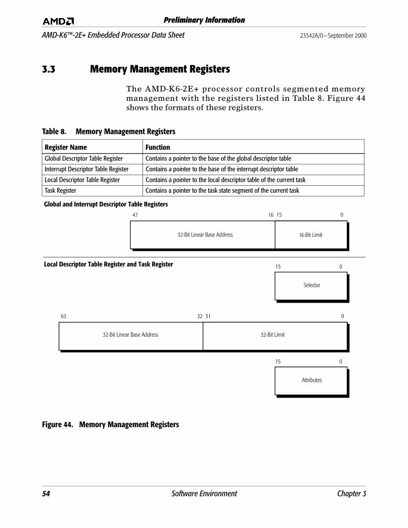
AMD-K6™-2E+ Embedded Processor Data Sheet 23542A/0—September 2000
Preliminary Information
3.3 Memory Management Registers
The AMD-K6-2E+ processor controls segmented memorymanagement with the registers listed in Table 8. Figure 44shows the formats of these registers.
Figure 44. Memory Management Registers
Table 8. Memory Management Registers
Register Name FunctionGlobal Descriptor Table Register Contains a pointer to the base of the global descriptor table
Interrupt Descriptor Table Register Contains a pointer to the base of the interrupt descriptor table
Local Descriptor Table Register Contains a pointer to the local descriptor table of the current task
Task Register Contains a pointer to the task state segment of the current task
15 0
16-Bit Limit
1647
32-Bit Linear Base Address
Global and Interrupt Descriptor Table Registers
31 063
32-Bit Limit
32
32-Bit Linear Base Address
15 0
Local Descriptor Table Register and Task Register
Attributes
15 0
Selector
54 Software Environment Chapter 3
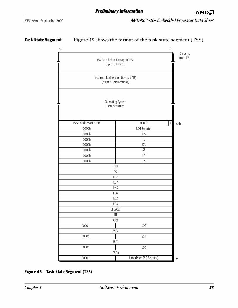
23542A/0—September 2000 AMD-K6™-2E+ Embedded Processor Data Sheet
Preliminary Information
Task State Segment Figure 45 shows the format of the task state segment (TSS).
Figure 45. Task State Segment (TSS)
31
Interrupt Redirection Bitmap (IRB)(eight 32-bit locations)
0
I/O Permission Bitmap (IOPB)(up to 8 Kbytes)
Operating SystemData Structure
Base Address of IOPB
LDT Selector0000h
0000h
0000h0000h
0000h
0000h
0000h
GS
FS
DSSS
CS
ES
EDI
ESIEBP
ESP
EBX
EDXECX
EAX
CR3
EFLAGS
EIP
0000h
0000h
0000h
0000h
SS2
SS1
SS0
Link (Prior TSS Selector)ESP0
ESP1
ESP2
TSS Limit from TR
64h
0
T0000h
Chapter 3 Software Environment 55
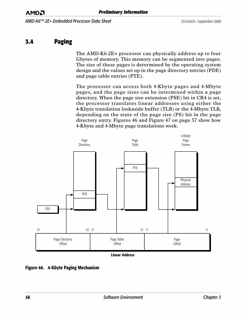
AMD-K6™-2E+ Embedded Processor Data Sheet 23542A/0—September 2000
Preliminary Information
3.4 Paging
The AMD-K6-2E+ processor can physically address up to fourGbytes of memory. This memory can be segmented into pages.The size of these pages is determined by the operating systemdesign and the values set up in the page directory entries (PDE)and page table entries (PTE).
The processor can access both 4-Kbyte pages and 4-Mbytepages, and the page sizes can be intermixed within a pagedirectory. When the page size extension (PSE) bit in CR4 is set,the processor translates linear addresses using either the4-Kbyte translation lookaside buffer (TLB) or the 4-Mbyte TLB,depending on the state of the page size (PS) bit in the pagedirectory entry. Figures 46 and Figure 47 on page 57 show how4-Kbyte and 4-Mbyte page translations work.
Figure 46. 4-Kbyte Paging Mechanism
Linear Address
PageDirectory
PageTable
4-KbytePage
Frame
CR3
011122131 22
Page DirectoryOffset
Page TableOffset
Page Offset
PDE
PTE
Physical Address
56 Software Environment Chapter 3
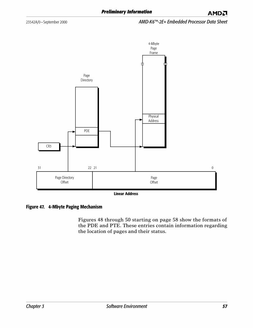
23542A/0—September 2000 AMD-K6™-2E+ Embedded Processor Data Sheet
Preliminary Information
Figure 47. 4-Mbyte Paging Mechanism
Figures 48 through 50 starting on page 58 show the formats ofthe PDE and PTE. These entries contain information regardingthe location of pages and their status.
Linear Address
PageDirectory
4-MbytePage
Frame
CR3
02131 22
Page DirectoryOffset
Page Offset
PDE
PhysicalAddress
Chapter 3 Software Environment 57
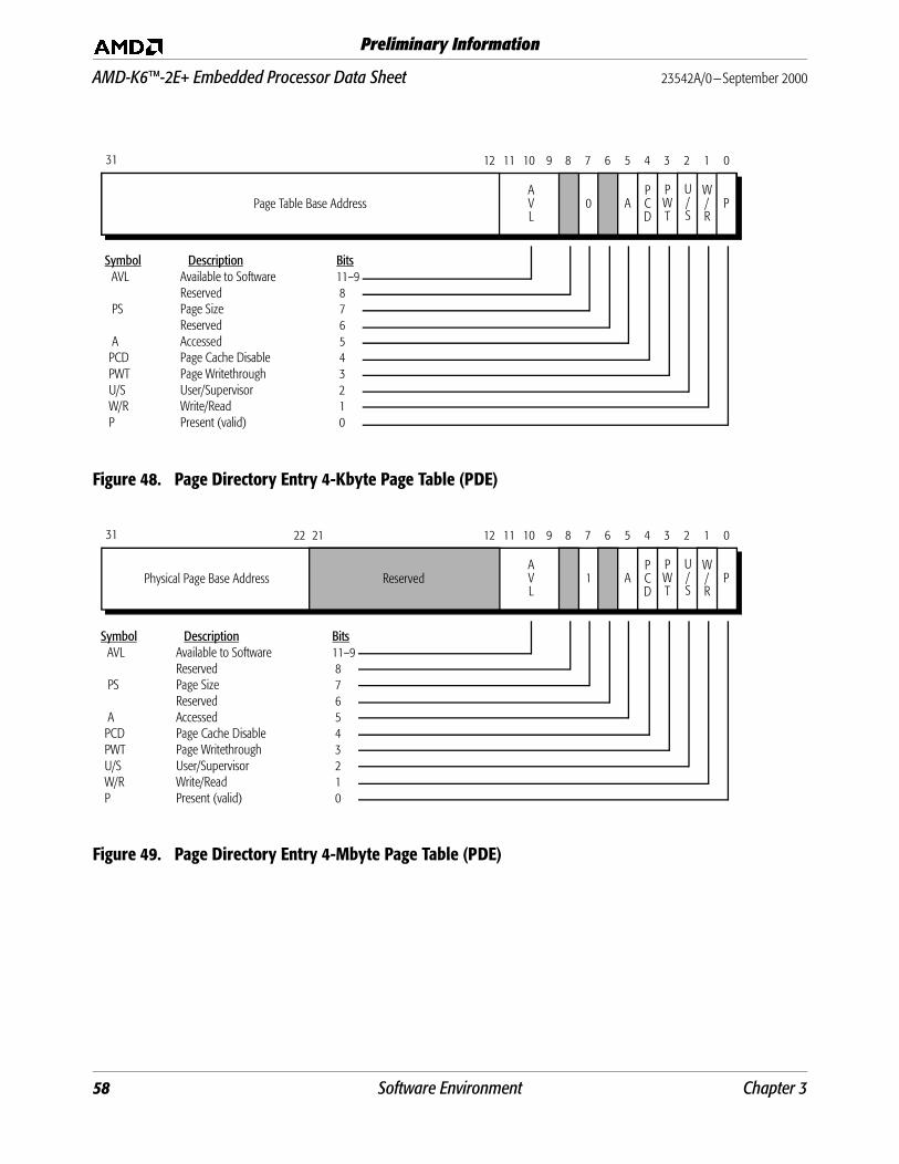
AMD-K6™-2E+ Embedded Processor Data Sheet 23542A/0—September 2000
Preliminary Information
Figure 48. Page Directory Entry 4-Kbyte Page Table (PDE)
Figure 49. Page Directory Entry 4-Mbyte Page Table (PDE)
8 7 6 5 4 3 2 1 031
PCD
U/S
W/R
9101112
AVL
0 APWT
PPage Table Base Address
Symbol Description BitsAVL Available to Software 11–9 Reserved 8 PS Page Size 7 Reserved 6 A Accessed 5PCD Page Cache Disable 4PWT Page Writethrough 3U/S User/Supervisor 2W/R Write/Read 1P Present (valid) 0
8 7 6 5 4 3 2 1 031
PCD
U/S
W/R
9101112
AVL
1 APWT
PPhysical Page Base Address Reserved
2122
Symbol Description BitsAVL Available to Software 11–9 Reserved 8 PS Page Size 7 Reserved 6 A Accessed 5PCD Page Cache Disable 4PWT Page Writethrough 3U/S User/Supervisor 2W/R Write/Read 1P Present (valid) 0
58 Software Environment Chapter 3
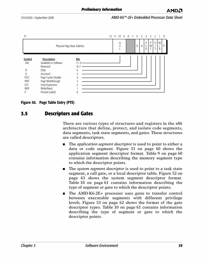
23542A/0—September 2000 AMD-K6™-2E+ Embedded Processor Data Sheet
Preliminary Information
Figure 50. Page Table Entry (PTE)
3.5 Descriptors and Gates
There are various types of structures and registers in the x86architecture that define, protect, and isolate code segments,data segments, task state segments, and gates. These structuresare called descriptors.
■ The application segment descriptor is used to point to either adata or code segment. Figure 51 on page 60 shows theapplication segment descriptor format. Table 9 on page 60contains information describing the memory segment typeto which the descriptor points.
■ The system segment descriptor is used to point to a task statesegment, a call gate, or a local descriptor table. Figure 52 onpage 61 shows the system segment descriptor format.Table 10 on page 61 contains information describing thetype of segment or gate to which the descriptor points.
■ The AMD-K6-2E+ processor uses gates to transfer controlbetween executable segments with different privilegelevels. Figure 53 on page 62 shows the format of the gatedescriptor types. Table 10 on page 61 contains informationdescribing the type of segment or gate to which thedescriptor points.
8 7 6 5 4 3 2 1 031
PCD
U/S
W/R
9101112
AVL
APWT
PPhysical Page Base Address D
Symbol Description BitsAVL Available to Software 11–9 Reserved 8–7 D Dirty 6 A Accessed 5PCD Page Cache Disable 4PWT Page Writethrough 3U/S User/Supervisor 2W/R Write/Read 1P Present (valid) 0
Chapter 3 Software Environment 59
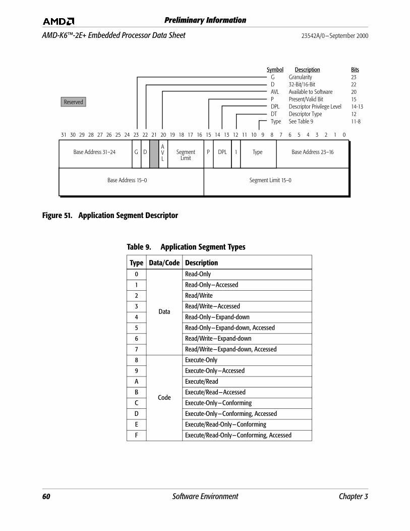
AMD-K6™-2E+ Embedded Processor Data Sheet 23542A/0—September 2000
Preliminary Information
Figure 51. Application Segment Descriptor
Base Address 15–0 Segment Limit 15–0
9 8 7 6 5 4 3 2 1 010111213141516171819202131 30 29 28 27 26 25 24 23 22
Segment Limit
P DPL 1 TypeAVL
G DBase Address 31–24 Base Address 23–16
Reserved
Symbol Description BitsG Granularity 23D 32-Bit/16-Bit 22AVL Available to Software 20P Present/Valid Bit 15DPL Descriptor Privilege Level 14-13DT Descriptor Type 12Type See Table 9 11-8
Table 9. Application Segment Types
Type Data/Code Description0
Data
Read-Only
1 Read-Only—Accessed
2 Read/Write
3 Read/Write—Accessed
4 Read-Only—Expand-down
5 Read-Only—Expand-down, Accessed
6 Read/Write—Expand-down
7 Read/Write—Expand-down, Accessed
8
Code
Execute-Only
9 Execute-Only—Accessed
A Execute/Read
B Execute/Read—Accessed
C Execute-Only—Conforming
D Execute-Only—Conforming, Accessed
E Execute/Read-Only—Conforming
F Execute/Read-Only—Conforming, Accessed
60 Software Environment Chapter 3
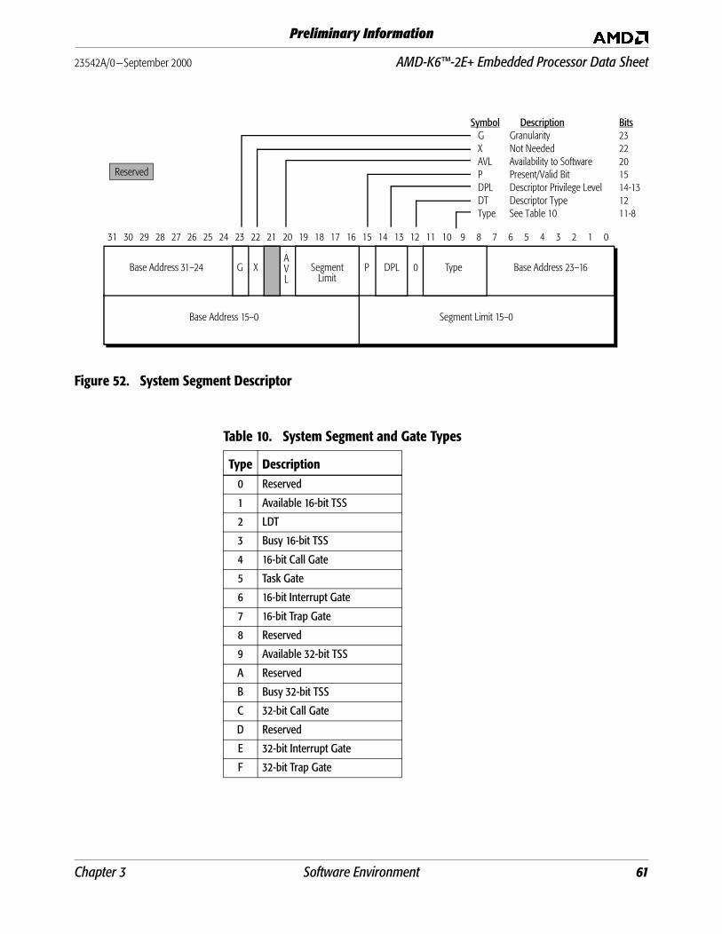
23542A/0—September 2000 AMD-K6™-2E+ Embedded Processor Data Sheet
Preliminary Information
Figure 52. System Segment Descriptor
Base Address 15–0 Segment Limit 15–0
9 8 7 6 5 4 3 2 1 010111213141516171819202131 30 29 28 27 26 25 24 23 22
Segment Limit
P DPL 0 TypeAVL
G XBase Address 31–24 Base Address 23–16
Reserved
Symbol Description BitsG Granularity 23X Not Needed 22AVL Availability to Software 20P Present/Valid Bit 15DPL Descriptor Privilege Level 14-13DT Descriptor Type 12Type See Table 10 11-8
Table 10. System Segment and Gate Types
Type Description0 Reserved
1 Available 16-bit TSS
2 LDT
3 Busy 16-bit TSS
4 16-bit Call Gate
5 Task Gate
6 16-bit Interrupt Gate
7 16-bit Trap Gate
8 Reserved
9 Available 32-bit TSS
A Reserved
B Busy 32-bit TSS
C 32-bit Call Gate
D Reserved
E 32-bit Interrupt Gate
F 32-bit Trap Gate
Chapter 3 Software Environment 61

AMD-K6™-2E+ Embedded Processor Data Sheet 23542A/0—September 2000
Preliminary Information
Figure 53. Gate Descriptor
3.6 Exceptions and Interrupts
Table 11 summarizes the exceptions and interrupts.
DPL 0 TypeOffset 31–16 P
Segment Selector Offset 15–0
9 8 7 6 5 4 3 2 1 010111213141516171819202131 30 29 28 27 26 25 24 23 22
Reserved
Symbol Description BitsP Present/Valid Bit 15DPL Descriptor Privilege Level 14-13DT Descriptor Type 12Type See Table 10 on page 61 11-8
Table 11. Summary of Exceptions and Interrupts
InterruptNumber Interrupt Type Cause
0 Divide by Zero Error DIV, IDIV
1 Debug Debug trap or fault
2 Non-Maskable Interrupt NMI signal sampled asserted
3 Breakpoint Int 3
4 Overflow INTO
5 Bounds Check BOUND
6 Invalid Opcode Invalid instruction
7 Device Not Available ESC and WAIT
8 Double Fault Fault occurs while handling a fault
9 Reserved - Interrupt 13 —
10 Invalid TSS Task switch to an invalid segment
11 Segment Not Present Instruction loads a segment and present bit is 0 (invalid segment)
12 Stack Segment Stack operation causes limit violation or present bit is 0
13 General Protection Segment related or miscellaneous invalid actions
14 Page Fault Page protection violation or a reference to missing page
16 Floating-Point Error Arithmetic error generated by floating-point instruction
17 Alignment Check Data reference to an unaligned operand. (The AC flag and the AM bit of CR0 are set to 1.)
0–255 Software Interrupt INT n
62 Software Environment Chapter 3
23542A/0—September 2000 AMD-K6™-2E+ Embedded Processor Data Sheet
Preliminary Information
3.7 Instructions Supported by the AMD-K6™-2E+ ProcessorThis section documents all of the x86 instructions supported bythe AMD-K6-2E+ processor. Tables 12 through 16 starting onpage 65 define the integer, floating-point, MMX, 3DNow!technology instructions, and 3DNow! technology digital signalprocessing (DSP) extensions for the AMD-K6-2E+ processor,respectively. For details about the MMX instructions, 3DNow!technology instructions, and 3DNow! technology DSPextensions refer to the following manuals:
■ MMX Instructions—AMD-K6® Processor MultimediaTechnology Manual, order# 20726
■ 3DNow! Technology Instructions—3DNow! TechnologyManual, order# 21928
■ 3DNow! Technology DSP Extensions—AMD Extensions to the3DNow! and MMX Instruction Set Manual, order# 22466
Each table shows the instruction mnemonic, opcode, modR/Mbyte, decode type, and RISC86 operation(s) for eachinstruction.
Instruction Mnemonic and Operand Types
The first column in these tables indicates the instructionmnemonic and operand types with the following notations:
■ disp16/32—16-bit or 32-bit displacement value
■ disp32/48—doubleword or 48-bit displacement value
■ disp8—8-bit displacement value
■ eXX—register width depending on the operand size
■ imm16/32—16-bit or 32-bit immediate value
■ imm8—8-bit immediate value
■ mem16/32—word or doubleword integer value in memory
■ mem32/48—doubleword or 48-bit integer value in memory
■ mem32real—32-bit floating-point value in memory
■ mem48—48-bit integer value in memory
■ mem64—64-bit integer value in memory
■ mem64real—64-bit floating-point value in memory
■ mem8—byte integer value in memory
■ mem80real—80-bit floating-point value in memory
■ mmreg—MMX/3DNow! register
Chapter 3 Software Environment 63
AMD-K6™-2E+ Embedded Processor Data Sheet 23542A/0—September 2000
Preliminary Information
■ mmreg1—MMX/3DNow! register defined by bits 5, 4, and 3of the modR/M byte
■ mmreg2—MMX/3DNow! register defined by bits 2, 1, and 0of the modR/M byte
■ mreg16/32—word or doubleword integer register, or word ordoubleword integer value in memory defined by themodR/M byte
■ mreg8—byte integer register or byte integer value inmemory defined by the modR/M byte
■ reg8—byte integer register defined by instruction byte(s) orbits 5, 4, and 3 of the modR/M byte
■ reg16/32—word or doubleword integer register defined byinstruction byte(s) or bits 5, 4, and 3 of the modR/M byte
Opcode Bytes The second and third columns list all applicable opcode bytes.
ModR/M Byte The fourth column lists the modR/M byte when used by theinstruction. The modR/M byte defines the instruction as aregister or memory form. If modR/M bits 7 and 6 aredocumented as mm (memory form), mm can only be 10b, 01b or00b.
Decode Type The fifth column lists the type of instruction decode—short,long, and vector. The AMD-K6-2E+ processor decode logic canprocess two short, one long, or one vector decode per clock.
RISC86® Operation The sixth column lists the type of RISC86 operation(s) requiredfor the instruction. The operation types and correspondingexecution units are as follows:
■ alu—either of the integer execution units
■ alux—integer X execution unit only
■ branch—branch condition unit
■ float—floating-point execution unit
■ limm—load immediate, instruction control unit
■ load, fload, mload—load unit
■ meu—multimedia execution units for MMX and 3DNow!instructions
■ store, fstore, mstore—store unit
64 Software Environment Chapter 3
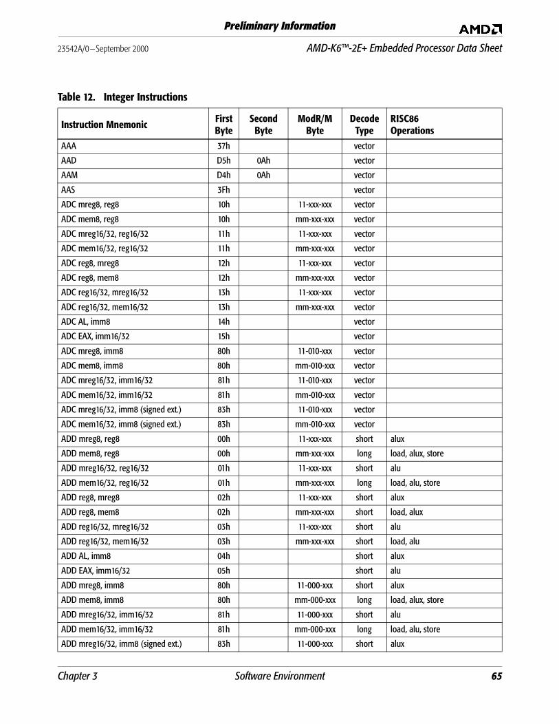
23542A/0—September 2000 AMD-K6™-2E+ Embedded Processor Data Sheet
Preliminary Information
Table 12. Integer Instructions
Instruction Mnemonic First Byte
Second Byte
ModR/M Byte
DecodeType
RISC86Operations
AAA 37h vector
AAD D5h 0Ah vector
AAM D4h 0Ah vector
AAS 3Fh vector
ADC mreg8, reg8 10h 11-xxx-xxx vector
ADC mem8, reg8 10h mm-xxx-xxx vector
ADC mreg16/32, reg16/32 11h 11-xxx-xxx vector
ADC mem16/32, reg16/32 11h mm-xxx-xxx vector
ADC reg8, mreg8 12h 11-xxx-xxx vector
ADC reg8, mem8 12h mm-xxx-xxx vector
ADC reg16/32, mreg16/32 13h 11-xxx-xxx vector
ADC reg16/32, mem16/32 13h mm-xxx-xxx vector
ADC AL, imm8 14h vector
ADC EAX, imm16/32 15h vector
ADC mreg8, imm8 80h 11-010-xxx vector
ADC mem8, imm8 80h mm-010-xxx vector
ADC mreg16/32, imm16/32 81h 11-010-xxx vector
ADC mem16/32, imm16/32 81h mm-010-xxx vector
ADC mreg16/32, imm8 (signed ext.) 83h 11-010-xxx vector
ADC mem16/32, imm8 (signed ext.) 83h mm-010-xxx vector
ADD mreg8, reg8 00h 11-xxx-xxx short alux
ADD mem8, reg8 00h mm-xxx-xxx long load, alux, store
ADD mreg16/32, reg16/32 01h 11-xxx-xxx short alu
ADD mem16/32, reg16/32 01h mm-xxx-xxx long load, alu, store
ADD reg8, mreg8 02h 11-xxx-xxx short alux
ADD reg8, mem8 02h mm-xxx-xxx short load, alux
ADD reg16/32, mreg16/32 03h 11-xxx-xxx short alu
ADD reg16/32, mem16/32 03h mm-xxx-xxx short load, alu
ADD AL, imm8 04h short alux
ADD EAX, imm16/32 05h short alu
ADD mreg8, imm8 80h 11-000-xxx short alux
ADD mem8, imm8 80h mm-000-xxx long load, alux, store
ADD mreg16/32, imm16/32 81h 11-000-xxx short alu
ADD mem16/32, imm16/32 81h mm-000-xxx long load, alu, store
ADD mreg16/32, imm8 (signed ext.) 83h 11-000-xxx short alux
Chapter 3 Software Environment 65
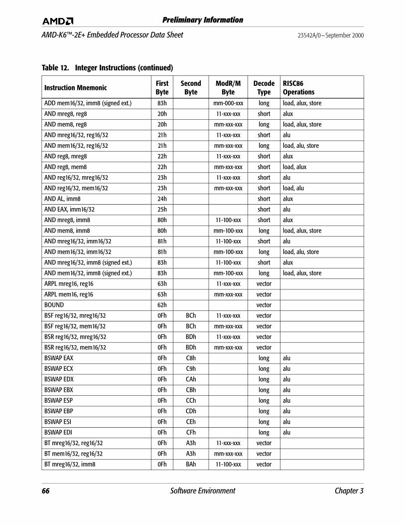
AMD-K6™-2E+ Embedded Processor Data Sheet 23542A/0—September 2000
Preliminary Information
ADD mem16/32, imm8 (signed ext.) 83h mm-000-xxx long load, alux, store
AND mreg8, reg8 20h 11-xxx-xxx short alux
AND mem8, reg8 20h mm-xxx-xxx long load, alux, store
AND mreg16/32, reg16/32 21h 11-xxx-xxx short alu
AND mem16/32, reg16/32 21h mm-xxx-xxx long load, alu, store
AND reg8, mreg8 22h 11-xxx-xxx short alux
AND reg8, mem8 22h mm-xxx-xxx short load, alux
AND reg16/32, mreg16/32 23h 11-xxx-xxx short alu
AND reg16/32, mem16/32 23h mm-xxx-xxx short load, alu
AND AL, imm8 24h short alux
AND EAX, imm16/32 25h short alu
AND mreg8, imm8 80h 11-100-xxx short alux
AND mem8, imm8 80h mm-100-xxx long load, alux, store
AND mreg16/32, imm16/32 81h 11-100-xxx short alu
AND mem16/32, imm16/32 81h mm-100-xxx long load, alu, store
AND mreg16/32, imm8 (signed ext.) 83h 11-100-xxx short alux
AND mem16/32, imm8 (signed ext.) 83h mm-100-xxx long load, alux, store
ARPL mreg16, reg16 63h 11-xxx-xxx vector
ARPL mem16, reg16 63h mm-xxx-xxx vector
BOUND 62h vector
BSF reg16/32, mreg16/32 0Fh BCh 11-xxx-xxx vector
BSF reg16/32, mem16/32 0Fh BCh mm-xxx-xxx vector
BSR reg16/32, mreg16/32 0Fh BDh 11-xxx-xxx vector
BSR reg16/32, mem16/32 0Fh BDh mm-xxx-xxx vector
BSWAP EAX 0Fh C8h long alu
BSWAP ECX 0Fh C9h long alu
BSWAP EDX 0Fh CAh long alu
BSWAP EBX 0Fh CBh long alu
BSWAP ESP 0Fh CCh long alu
BSWAP EBP 0Fh CDh long alu
BSWAP ESI 0Fh CEh long alu
BSWAP EDI 0Fh CFh long alu
BT mreg16/32, reg16/32 0Fh A3h 11-xxx-xxx vector
BT mem16/32, reg16/32 0Fh A3h mm-xxx-xxx vector
BT mreg16/32, imm8 0Fh BAh 11-100-xxx vector
Table 12. Integer Instructions (continued)
Instruction Mnemonic First Byte
Second Byte
ModR/M Byte
DecodeType
RISC86Operations
66 Software Environment Chapter 3

23542A/0—September 2000 AMD-K6™-2E+ Embedded Processor Data Sheet
Preliminary Information
BT mem16/32, imm8 0Fh BAh mm-100-xxx vector
BTC mreg16/32, reg16/32 0Fh BBh 11-xxx-xxx vector
BTC mem16/32, reg16/32 0Fh BBh mm-xxx-xxx vector
BTC mreg16/32, imm8 0Fh BAh 11-111-xxx vector
BTC mem16/32, imm8 0Fh BAh mm-111-xxx vector
BTR mreg16/32, reg16/32 0Fh B3h 11-xxx-xxx vector
BTR mem16/32, reg16/32 0Fh B3h mm-xxx-xxx vector
BTR mreg16/32, imm8 0Fh BAh 11-110-xxx vector
BTR mem16/32, imm8 0Fh BAh mm-110-xxx vector
BTS mreg16/32, reg16/32 0Fh ABh 11-xxx-xxx vector
BTS mem16/32, reg16/32 0Fh ABh mm-xxx-xxx vector
BTS mreg16/32, imm8 0Fh BAh 11-101-xxx vector
BTS mem16/32, imm8 0Fh BAh mm-101-xxx vector
CALL full pointer 9Ah vector
CALL near imm16/32 E8h short store
CALL mem16:16/32 FFh 11-011-xxx vector
CALL near mreg32 (indirect) FFh 11-010-xxx vector
CALL near mem32 (indirect) FFh mm-010-xxx vector
CBW/CWDE EAX 98h vector
CLC F8h vector
CLD FCh vector
CLI FAh vector
CLTS 0Fh 06h vector
CMC F5h vector
CMP mreg8, reg8 38h 11-xxx-xxx short alux
CMP mem8, reg8 38h mm-xxx-xxx short load, alux
CMP mreg16/32, reg16/32 39h 11-xxx-xxx short alu
CMP mem16/32, reg16/32 39h mm-xxx-xxx short load, alu
CMP reg8, mreg8 3Ah 11-xxx-xxx short alux
CMP reg8, mem8 3Ah mm-xxx-xxx short load, alux
CMP reg16/32, mreg16/32 3Bh 11-xxx-xxx short alu
CMP reg16/32, mem16/32 3Bh mm-xxx-xxx short load, alu
CMP AL, imm8 3Ch short alux
CMP EAX, imm16/32 3Dh short alu
CMP mreg8, imm8 80h 11-111-xxx short alux
Table 12. Integer Instructions (continued)
Instruction Mnemonic First Byte
Second Byte
ModR/M Byte
DecodeType
RISC86Operations
Chapter 3 Software Environment 67
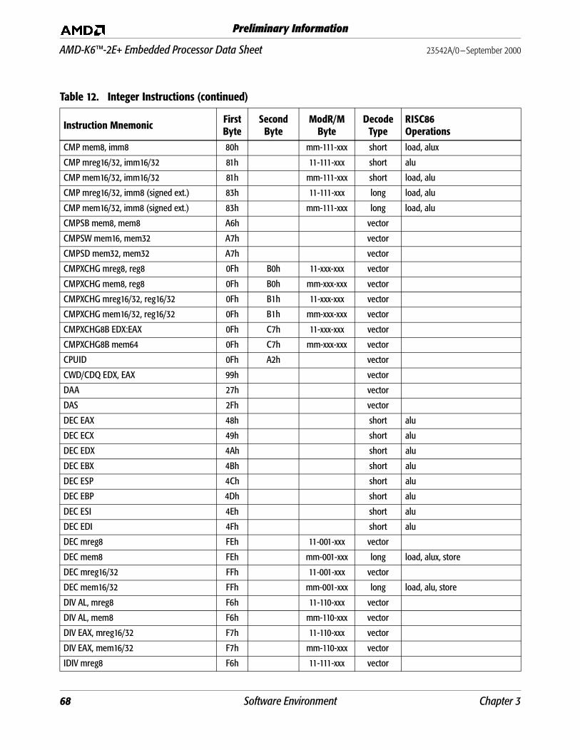
AMD-K6™-2E+ Embedded Processor Data Sheet 23542A/0—September 2000
Preliminary Information
CMP mem8, imm8 80h mm-111-xxx short load, alux
CMP mreg16/32, imm16/32 81h 11-111-xxx short alu
CMP mem16/32, imm16/32 81h mm-111-xxx short load, alu
CMP mreg16/32, imm8 (signed ext.) 83h 11-111-xxx long load, alu
CMP mem16/32, imm8 (signed ext.) 83h mm-111-xxx long load, alu
CMPSB mem8, mem8 A6h vector
CMPSW mem16, mem32 A7h vector
CMPSD mem32, mem32 A7h vector
CMPXCHG mreg8, reg8 0Fh B0h 11-xxx-xxx vector
CMPXCHG mem8, reg8 0Fh B0h mm-xxx-xxx vector
CMPXCHG mreg16/32, reg16/32 0Fh B1h 11-xxx-xxx vector
CMPXCHG mem16/32, reg16/32 0Fh B1h mm-xxx-xxx vector
CMPXCHG8B EDX:EAX 0Fh C7h 11-xxx-xxx vector
CMPXCHG8B mem64 0Fh C7h mm-xxx-xxx vector
CPUID 0Fh A2h vector
CWD/CDQ EDX, EAX 99h vector
DAA 27h vector
DAS 2Fh vector
DEC EAX 48h short alu
DEC ECX 49h short alu
DEC EDX 4Ah short alu
DEC EBX 4Bh short alu
DEC ESP 4Ch short alu
DEC EBP 4Dh short alu
DEC ESI 4Eh short alu
DEC EDI 4Fh short alu
DEC mreg8 FEh 11-001-xxx vector
DEC mem8 FEh mm-001-xxx long load, alux, store
DEC mreg16/32 FFh 11-001-xxx vector
DEC mem16/32 FFh mm-001-xxx long load, alu, store
DIV AL, mreg8 F6h 11-110-xxx vector
DIV AL, mem8 F6h mm-110-xxx vector
DIV EAX, mreg16/32 F7h 11-110-xxx vector
DIV EAX, mem16/32 F7h mm-110-xxx vector
IDIV mreg8 F6h 11-111-xxx vector
Table 12. Integer Instructions (continued)
Instruction Mnemonic First Byte
Second Byte
ModR/M Byte
DecodeType
RISC86Operations
68 Software Environment Chapter 3
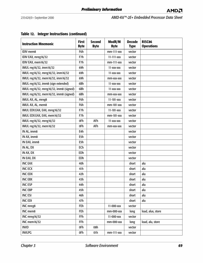
23542A/0—September 2000 AMD-K6™-2E+ Embedded Processor Data Sheet
Preliminary Information
IDIV mem8 F6h mm-111-xxx vector
IDIV EAX, mreg16/32 F7h 11-111-xxx vector
IDIV EAX, mem16/32 F7h mm-111-xxx vector
IMUL reg16/32, imm16/32 69h 11-xxx-xxx vector
IMUL reg16/32, mreg16/32, imm16/32 69h 11-xxx-xxx vector
IMUL reg16/32, mem16/32, imm16/32 69h mm-xxx-xxx vector
IMUL reg16/32, imm8 (sign extended) 6Bh 11-xxx-xxx vector
IMUL reg16/32, mreg16/32, imm8 (signed) 6Bh 11-xxx-xxx vector
IMUL reg16/32, mem16/32, imm8 (signed) 6Bh mm-xxx-xxx vector
IMUL AX, AL, mreg8 F6h 11-101-xxx vector
IMUL AX, AL, mem8 F6h mm-101-xxx vector
IMUL EDX:EAX, EAX, mreg16/32 F7h 11-101-xxx vector
IMUL EDX:EAX, EAX, mem16/32 F7h mm-101-xxx vector
IMUL reg16/32, mreg16/32 0Fh AFh 11-xxx-xxx vector
IMUL reg16/32, mem16/32 0Fh AFh mm-xxx-xxx vector
IN AL, imm8 E4h vector
IN AX, imm8 E5h vector
IN EAX, imm8 E5h vector
IN AL, DX ECh vector
IN AX, DX EDh vector
IN EAX, DX EDh vector
INC EAX 40h short alu
INC ECX 41h short alu
INC EDX 42h short alu
INC EBX 43h short alu
INC ESP 44h short alu
INC EBP 45h short alu
INC ESI 46h short alu
INC EDI 47h short alu
INC mreg8 FEh 11-000-xxx vector
INC mem8 FEh mm-000-xxx long load, alux, store
INC mreg16/32 FFh 11-000-xxx vector
INC mem16/32 FFh mm-000-xxx long load, alu, store
INVD 0Fh 08h vector
INVLPG 0Fh 01h mm-111-xxx vector
Table 12. Integer Instructions (continued)
Instruction Mnemonic First Byte
Second Byte
ModR/M Byte
DecodeType
RISC86Operations
Chapter 3 Software Environment 69
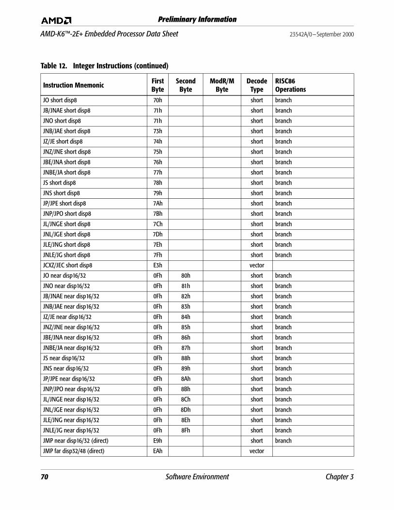
AMD-K6™-2E+ Embedded Processor Data Sheet 23542A/0—September 2000
Preliminary Information
JO short disp8 70h short branch
JB/JNAE short disp8 71h short branch
JNO short disp8 71h short branch
JNB/JAE short disp8 73h short branch
JZ/JE short disp8 74h short branch
JNZ/JNE short disp8 75h short branch
JBE/JNA short disp8 76h short branch
JNBE/JA short disp8 77h short branch
JS short disp8 78h short branch
JNS short disp8 79h short branch
JP/JPE short disp8 7Ah short branch
JNP/JPO short disp8 7Bh short branch
JL/JNGE short disp8 7Ch short branch
JNL/JGE short disp8 7Dh short branch
JLE/JNG short disp8 7Eh short branch
JNLE/JG short disp8 7Fh short branch
JCXZ/JEC short disp8 E3h vector
JO near disp16/32 0Fh 80h short branch
JNO near disp16/32 0Fh 81h short branch
JB/JNAE near disp16/32 0Fh 82h short branch
JNB/JAE near disp16/32 0Fh 83h short branch
JZ/JE near disp16/32 0Fh 84h short branch
JNZ/JNE near disp16/32 0Fh 85h short branch
JBE/JNA near disp16/32 0Fh 86h short branch
JNBE/JA near disp16/32 0Fh 87h short branch
JS near disp16/32 0Fh 88h short branch
JNS near disp16/32 0Fh 89h short branch
JP/JPE near disp16/32 0Fh 8Ah short branch
JNP/JPO near disp16/32 0Fh 8Bh short branch
JL/JNGE near disp16/32 0Fh 8Ch short branch
JNL/JGE near disp16/32 0Fh 8Dh short branch
JLE/JNG near disp16/32 0Fh 8Eh short branch
JNLE/JG near disp16/32 0Fh 8Fh short branch
JMP near disp16/32 (direct) E9h short branch
JMP far disp32/48 (direct) EAh vector
Table 12. Integer Instructions (continued)
Instruction Mnemonic First Byte
Second Byte
ModR/M Byte
DecodeType
RISC86Operations
70 Software Environment Chapter 3

23542A/0—September 2000 AMD-K6™-2E+ Embedded Processor Data Sheet
Preliminary Information
JMP disp8 (short) EBh short branch
JMP far mreg32 (indirect) EFh 11-101-xxx vector
JMP far mem32 (indirect) EFh mm-101-xxx vector
JMP near mreg16/32 (indirect) FFh 11-100-xxx vector
JMP near mem16/32 (indirect) FFh mm-100-xxx vector
LAHF 9Fh vector
LAR reg16/32, mreg16/32 0Fh 02h 11-xxx-xxx vector
LAR reg16/32, mem16/32 0Fh 02h mm-xxx-xxx vector
LDS reg16/32, mem32/48 C5h mm-xxx-xxx vector
LEA reg16/32, mem16/32 8Dh mm-xxx-xxx short load, alu
LEAVE C9h long load, alu, alu
LES reg16/32, mem32/48 C4h mm-xxx-xxx vector
LFS reg16/32, mem32/48 0Fh B4h vector
LGDT mem48 0Fh 01h mm-010-xxx vector
LGS reg16/32, mem32/48 0Fh B5h vector
LIDT mem48 0Fh 01h mm-011-xxx vector
LLDT mreg16 0Fh 00h 11-010-xxx vector
LLDT mem16 0Fh 00h mm-010-xxx vector
LMSW mreg16 0Fh 01h 11-100-xxx vector
LMSW mem16 0Fh 01h mm-100-xxx vector
LODSB AL, mem8 ACh long load, alu
LODSW AX, mem16 ADh long load, alu
LODSD EAX, mem32 ADh long load, alu
LOOP disp8 E2h short alu, branch
LOOPE/LOOPZ disp8 E1h vector
LOOPNE/LOOPNZ disp8 E0h vector
LSL reg16/32, mreg16/32 0Fh 03h 11-xxx-xxx vector
LSL reg16/32, mem16/32 0Fh 03h mm-xxx-xxx vector
LSS reg16/32, mem32/48 0Fh B2h mm-xxx-xxx vector
LTR mreg16 0Fh 00h 11-011-xxx vector
LTR mem16 0Fh 00h mm-011-xxx vector
MOV mreg8, reg8 88h 11-xxx-xxx short alux
MOV mem8, reg8 88h mm-xxx-xxx short store
MOV mreg16/32, reg16/32 89h 11-xxx-xxx short alu
MOV mem16/32, reg16/32 89h mm-xxx-xxx short store
Table 12. Integer Instructions (continued)
Instruction Mnemonic First Byte
Second Byte
ModR/M Byte
DecodeType
RISC86Operations
Chapter 3 Software Environment 71
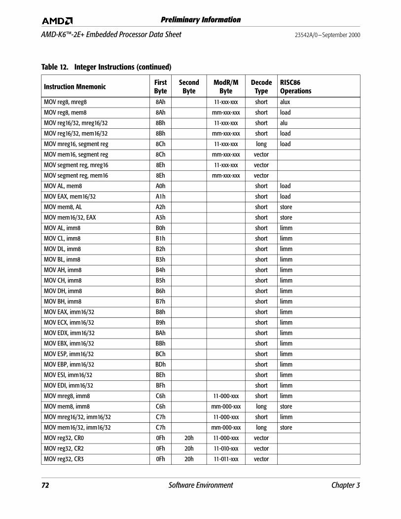
AMD-K6™-2E+ Embedded Processor Data Sheet 23542A/0—September 2000
Preliminary Information
MOV reg8, mreg8 8Ah 11-xxx-xxx short alux
MOV reg8, mem8 8Ah mm-xxx-xxx short load
MOV reg16/32, mreg16/32 8Bh 11-xxx-xxx short alu
MOV reg16/32, mem16/32 8Bh mm-xxx-xxx short load
MOV mreg16, segment reg 8Ch 11-xxx-xxx long load
MOV mem16, segment reg 8Ch mm-xxx-xxx vector
MOV segment reg, mreg16 8Eh 11-xxx-xxx vector
MOV segment reg, mem16 8Eh mm-xxx-xxx vector
MOV AL, mem8 A0h short load
MOV EAX, mem16/32 A1h short load
MOV mem8, AL A2h short store
MOV mem16/32, EAX A3h short store
MOV AL, imm8 B0h short limm
MOV CL, imm8 B1h short limm
MOV DL, imm8 B2h short limm
MOV BL, imm8 B3h short limm
MOV AH, imm8 B4h short limm
MOV CH, imm8 B5h short limm
MOV DH, imm8 B6h short limm
MOV BH, imm8 B7h short limm
MOV EAX, imm16/32 B8h short limm
MOV ECX, imm16/32 B9h short limm
MOV EDX, imm16/32 BAh short limm
MOV EBX, imm16/32 BBh short limm
MOV ESP, imm16/32 BCh short limm
MOV EBP, imm16/32 BDh short limm
MOV ESI, imm16/32 BEh short limm
MOV EDI, imm16/32 BFh short limm
MOV mreg8, imm8 C6h 11-000-xxx short limm
MOV mem8, imm8 C6h mm-000-xxx long store
MOV mreg16/32, imm16/32 C7h 11-000-xxx short limm
MOV mem16/32, imm16/32 C7h mm-000-xxx long store
MOV reg32, CR0 0Fh 20h 11-000-xxx vector
MOV reg32, CR2 0Fh 20h 11-010-xxx vector
MOV reg32, CR3 0Fh 20h 11-011-xxx vector
Table 12. Integer Instructions (continued)
Instruction Mnemonic First Byte
Second Byte
ModR/M Byte
DecodeType
RISC86Operations
72 Software Environment Chapter 3
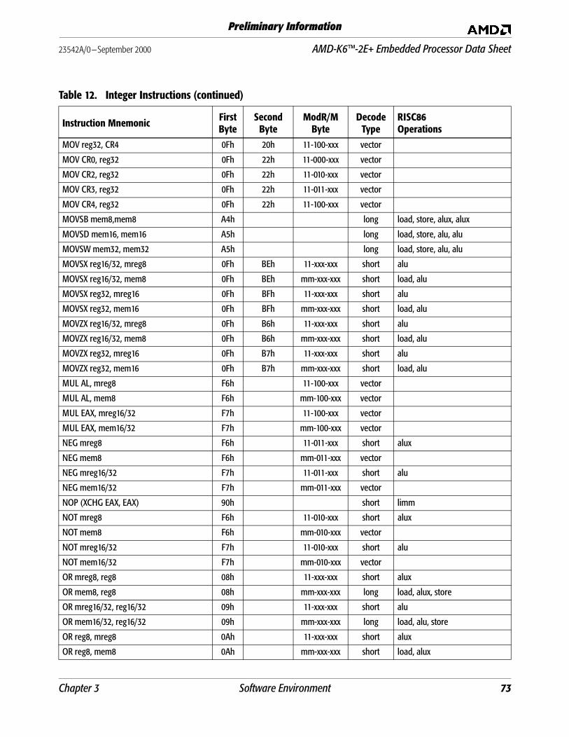
23542A/0—September 2000 AMD-K6™-2E+ Embedded Processor Data Sheet
Preliminary Information
MOV reg32, CR4 0Fh 20h 11-100-xxx vector
MOV CR0, reg32 0Fh 22h 11-000-xxx vector
MOV CR2, reg32 0Fh 22h 11-010-xxx vector
MOV CR3, reg32 0Fh 22h 11-011-xxx vector
MOV CR4, reg32 0Fh 22h 11-100-xxx vector
MOVSB mem8,mem8 A4h long load, store, alux, alux
MOVSD mem16, mem16 A5h long load, store, alu, alu
MOVSW mem32, mem32 A5h long load, store, alu, alu
MOVSX reg16/32, mreg8 0Fh BEh 11-xxx-xxx short alu
MOVSX reg16/32, mem8 0Fh BEh mm-xxx-xxx short load, alu
MOVSX reg32, mreg16 0Fh BFh 11-xxx-xxx short alu
MOVSX reg32, mem16 0Fh BFh mm-xxx-xxx short load, alu
MOVZX reg16/32, mreg8 0Fh B6h 11-xxx-xxx short alu
MOVZX reg16/32, mem8 0Fh B6h mm-xxx-xxx short load, alu
MOVZX reg32, mreg16 0Fh B7h 11-xxx-xxx short alu
MOVZX reg32, mem16 0Fh B7h mm-xxx-xxx short load, alu
MUL AL, mreg8 F6h 11-100-xxx vector
MUL AL, mem8 F6h mm-100-xxx vector
MUL EAX, mreg16/32 F7h 11-100-xxx vector
MUL EAX, mem16/32 F7h mm-100-xxx vector
NEG mreg8 F6h 11-011-xxx short alux
NEG mem8 F6h mm-011-xxx vector
NEG mreg16/32 F7h 11-011-xxx short alu
NEG mem16/32 F7h mm-011-xxx vector
NOP (XCHG EAX, EAX) 90h short limm
NOT mreg8 F6h 11-010-xxx short alux
NOT mem8 F6h mm-010-xxx vector
NOT mreg16/32 F7h 11-010-xxx short alu
NOT mem16/32 F7h mm-010-xxx vector
OR mreg8, reg8 08h 11-xxx-xxx short alux
OR mem8, reg8 08h mm-xxx-xxx long load, alux, store
OR mreg16/32, reg16/32 09h 11-xxx-xxx short alu
OR mem16/32, reg16/32 09h mm-xxx-xxx long load, alu, store
OR reg8, mreg8 0Ah 11-xxx-xxx short alux
OR reg8, mem8 0Ah mm-xxx-xxx short load, alux
Table 12. Integer Instructions (continued)
Instruction Mnemonic First Byte
Second Byte
ModR/M Byte
DecodeType
RISC86Operations
Chapter 3 Software Environment 73
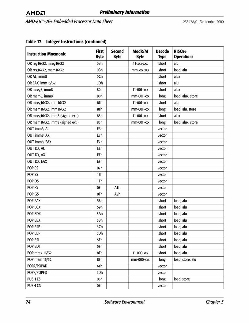
AMD-K6™-2E+ Embedded Processor Data Sheet 23542A/0—September 2000
Preliminary Information
OR reg16/32, mreg16/32 0Bh 11-xxx-xxx short alu
OR reg16/32, mem16/32 0Bh mm-xxx-xxx short load, alu
OR AL, imm8 0Ch short alux
OR EAX, imm16/32 0Dh short alu
OR mreg8, imm8 80h 11-001-xxx short alux
OR mem8, imm8 80h mm-001-xxx long load, alux, store
OR mreg16/32, imm16/32 81h 11-001-xxx short alu
OR mem16/32, imm16/32 81h mm-001-xxx long load, alu, store
OR mreg16/32, imm8 (signed ext.) 83h 11-001-xxx short alux
OR mem16/32, imm8 (signed ext.) 83h mm-001-xxx long load, alux, store
OUT imm8, AL E6h vector
OUT imm8, AX E7h vector
OUT imm8, EAX E7h vector
OUT DX, AL EEh vector
OUT DX, AX EFh vector
OUT DX, EAX EFh vector
POP ES 07h vector
POP SS 17h vector
POP DS 1Fh vector
POP FS 0Fh A1h vector
POP GS 0Fh A9h vector
POP EAX 58h short load, alu
POP ECX 59h short load, alu
POP EDX 5Ah short load, alu
POP EBX 5Bh short load, alu
POP ESP 5Ch short load, alu
POP EBP 5Dh short load, alu
POP ESI 5Eh short load, alu
POP EDI 5Fh short load, alu
POP mreg 16/32 8Fh 11-000-xxx short load, alu
POP mem 16/32 8Fh mm-000-xxx long load, store, alu
POPA/POPAD 61h vector
POPF/POPFD 9Dh vector
PUSH ES 06h long load, store
PUSH CS 0Eh vector
Table 12. Integer Instructions (continued)
Instruction Mnemonic First Byte
Second Byte
ModR/M Byte
DecodeType
RISC86Operations
74 Software Environment Chapter 3
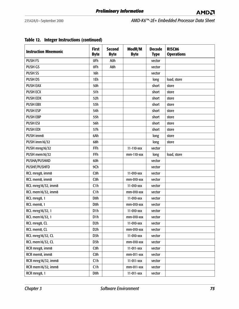
23542A/0—September 2000 AMD-K6™-2E+ Embedded Processor Data Sheet
Preliminary Information
PUSH FS 0Fh A0h vector
PUSH GS 0Fh A8h vector
PUSH SS 16h vector
PUSH DS 1Eh long load, store
PUSH EAX 50h short store
PUSH ECX 51h short store
PUSH EDX 52h short store
PUSH EBX 53h short store
PUSH ESP 54h short store
PUSH EBP 55h short store
PUSH ESI 56h short store
PUSH EDI 57h short store
PUSH imm8 6Ah long store
PUSH imm16/32 68h long store
PUSH mreg16/32 FFh 11-110-xxx vector
PUSH mem16/32 FFh mm-110-xxx long load, store
PUSHA/PUSHAD 60h vector
PUSHF/PUSHFD 9Ch vector
RCL mreg8, imm8 C0h 11-010-xxx vector
RCL mem8, imm8 C0h mm-010-xxx vector
RCL mreg16/32, imm8 C1h 11-010-xxx vector
RCL mem16/32, imm8 C1h mm-010-xxx vector
RCL mreg8, 1 D0h 11-010-xxx vector
RCL mem8, 1 D0h mm-010-xxx vector
RCL mreg16/32, 1 D1h 11-010-xxx vector
RCL mem16/32, 1 D1h mm-010-xxx vector
RCL mreg8, CL D2h 11-010-xxx vector
RCL mem8, CL D2h mm-010-xxx vector
RCL mreg16/32, CL D3h 11-010-xxx vector
RCL mem16/32, CL D3h mm-010-xxx vector
RCR mreg8, imm8 C0h 11-011-xxx vector
RCR mem8, imm8 C0h mm-011-xxx vector
RCR mreg16/32, imm8 C1h 11-011-xxx vector
RCR mem16/32, imm8 C1h mm-011-xxx vector
RCR mreg8, 1 D0h 11-011-xxx vector
Table 12. Integer Instructions (continued)
Instruction Mnemonic First Byte
Second Byte
ModR/M Byte
DecodeType
RISC86Operations
Chapter 3 Software Environment 75
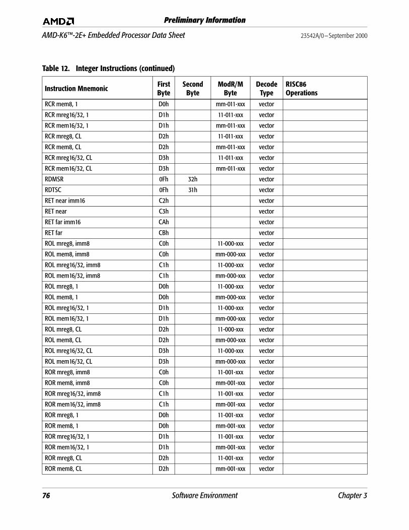
AMD-K6™-2E+ Embedded Processor Data Sheet 23542A/0—September 2000
Preliminary Information
RCR mem8, 1 D0h mm-011-xxx vector
RCR mreg16/32, 1 D1h 11-011-xxx vector
RCR mem16/32, 1 D1h mm-011-xxx vector
RCR mreg8, CL D2h 11-011-xxx vector
RCR mem8, CL D2h mm-011-xxx vector
RCR mreg16/32, CL D3h 11-011-xxx vector
RCR mem16/32, CL D3h mm-011-xxx vector
RDMSR 0Fh 32h vector
RDTSC 0Fh 31h vector
RET near imm16 C2h vector
RET near C3h vector
RET far imm16 CAh vector
RET far CBh vector
ROL mreg8, imm8 C0h 11-000-xxx vector
ROL mem8, imm8 C0h mm-000-xxx vector
ROL mreg16/32, imm8 C1h 11-000-xxx vector
ROL mem16/32, imm8 C1h mm-000-xxx vector
ROL mreg8, 1 D0h 11-000-xxx vector
ROL mem8, 1 D0h mm-000-xxx vector
ROL mreg16/32, 1 D1h 11-000-xxx vector
ROL mem16/32, 1 D1h mm-000-xxx vector
ROL mreg8, CL D2h 11-000-xxx vector
ROL mem8, CL D2h mm-000-xxx vector
ROL mreg16/32, CL D3h 11-000-xxx vector
ROL mem16/32, CL D3h mm-000-xxx vector
ROR mreg8, imm8 C0h 11-001-xxx vector
ROR mem8, imm8 C0h mm-001-xxx vector
ROR mreg16/32, imm8 C1h 11-001-xxx vector
ROR mem16/32, imm8 C1h mm-001-xxx vector
ROR mreg8, 1 D0h 11-001-xxx vector
ROR mem8, 1 D0h mm-001-xxx vector
ROR mreg16/32, 1 D1h 11-001-xxx vector
ROR mem16/32, 1 D1h mm-001-xxx vector
ROR mreg8, CL D2h 11-001-xxx vector
ROR mem8, CL D2h mm-001-xxx vector
Table 12. Integer Instructions (continued)
Instruction Mnemonic First Byte
Second Byte
ModR/M Byte
DecodeType
RISC86Operations
76 Software Environment Chapter 3

23542A/0—September 2000 AMD-K6™-2E+ Embedded Processor Data Sheet
Preliminary Information
ROR mreg16/32, CL D3h 11-001-xxx vector
ROR mem16/32, CL D3h mm-001-xxx vector
RSM 0Fh AAh vector
SAHF 9Eh vector
SAR mreg8, imm8 C0h 11-111-xxx short alux
SAR mem8, imm8 C0h mm-111-xxx vector
SAR mreg16/32, imm8 C1h 11-111-xxx short alu
SAR mem16/32, imm8 C1h mm-111-xxx vector
SAR mreg8, 1 D0h 11-111-xxx short alux
SAR mem8, 1 D0h mm-111-xxx vector
SAR mreg16/32, 1 D1h 11-111-xxx short alu
SAR mem16/32, 1 D1h mm-111-xxx vector
SAR mreg8, CL D2h 11-111-xxx short alux
SAR mem8, CL D2h mm-111-xxx vector
SAR mreg16/32, CL D3h 11-111-xxx short alu
SAR mem16/32, CL D3h mm-111-xxx vector
SBB mreg8, reg8 18h 11-xxx-xxx vector
SBB mem8, reg8 18h mm-xxx-xxx vector
SBB mreg16/32, reg16/32 19h 11-xxx-xxx vector
SBB mem16/32, reg16/32 19h mm-xxx-xxx vector
SBB reg8, mreg8 1Ah 11-xxx-xxx vector
SBB reg8, mem8 1Ah mm-xxx-xxx vector
SBB reg16/32, mreg16/32 1Bh 11-xxx-xxx vector
SBB reg16/32, mem16/32 1Bh mm-xxx-xxx vector
SBB AL, imm8 1Ch vector
SBB EAX, imm16/32 1Dh vector
SBB mreg8, imm8 80h 11-011-xxx vector
SBB mem8, imm8 80h mm-011-xxx vector
SBB mreg16/32, imm16/32 81h 11-011-xxx vector
SBB mem16/32, imm16/32 81h mm-011-xxx vector
SBB mreg16/32, imm8 (signed ext.) 83h 11-011-xxx vector
SBB mem16/32, imm8 (signed ext.) 83h mm-011-xxx vector
SCASB AL, mem8 AEh vector
SCASW AX, mem16 AFh vector
SCASD EAX, mem32 AFh vector
Table 12. Integer Instructions (continued)
Instruction Mnemonic First Byte
Second Byte
ModR/M Byte
DecodeType
RISC86Operations
Chapter 3 Software Environment 77
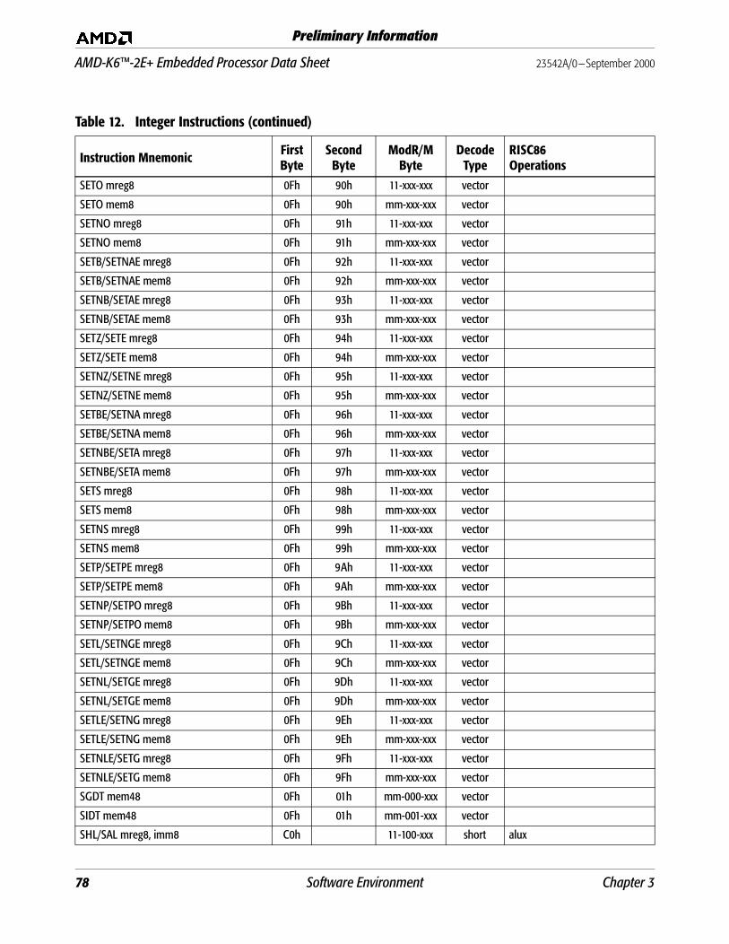
AMD-K6™-2E+ Embedded Processor Data Sheet 23542A/0—September 2000
Preliminary Information
SETO mreg8 0Fh 90h 11-xxx-xxx vector
SETO mem8 0Fh 90h mm-xxx-xxx vector
SETNO mreg8 0Fh 91h 11-xxx-xxx vector
SETNO mem8 0Fh 91h mm-xxx-xxx vector
SETB/SETNAE mreg8 0Fh 92h 11-xxx-xxx vector
SETB/SETNAE mem8 0Fh 92h mm-xxx-xxx vector
SETNB/SETAE mreg8 0Fh 93h 11-xxx-xxx vector
SETNB/SETAE mem8 0Fh 93h mm-xxx-xxx vector
SETZ/SETE mreg8 0Fh 94h 11-xxx-xxx vector
SETZ/SETE mem8 0Fh 94h mm-xxx-xxx vector
SETNZ/SETNE mreg8 0Fh 95h 11-xxx-xxx vector
SETNZ/SETNE mem8 0Fh 95h mm-xxx-xxx vector
SETBE/SETNA mreg8 0Fh 96h 11-xxx-xxx vector
SETBE/SETNA mem8 0Fh 96h mm-xxx-xxx vector
SETNBE/SETA mreg8 0Fh 97h 11-xxx-xxx vector
SETNBE/SETA mem8 0Fh 97h mm-xxx-xxx vector
SETS mreg8 0Fh 98h 11-xxx-xxx vector
SETS mem8 0Fh 98h mm-xxx-xxx vector
SETNS mreg8 0Fh 99h 11-xxx-xxx vector
SETNS mem8 0Fh 99h mm-xxx-xxx vector
SETP/SETPE mreg8 0Fh 9Ah 11-xxx-xxx vector
SETP/SETPE mem8 0Fh 9Ah mm-xxx-xxx vector
SETNP/SETPO mreg8 0Fh 9Bh 11-xxx-xxx vector
SETNP/SETPO mem8 0Fh 9Bh mm-xxx-xxx vector
SETL/SETNGE mreg8 0Fh 9Ch 11-xxx-xxx vector
SETL/SETNGE mem8 0Fh 9Ch mm-xxx-xxx vector
SETNL/SETGE mreg8 0Fh 9Dh 11-xxx-xxx vector
SETNL/SETGE mem8 0Fh 9Dh mm-xxx-xxx vector
SETLE/SETNG mreg8 0Fh 9Eh 11-xxx-xxx vector
SETLE/SETNG mem8 0Fh 9Eh mm-xxx-xxx vector
SETNLE/SETG mreg8 0Fh 9Fh 11-xxx-xxx vector
SETNLE/SETG mem8 0Fh 9Fh mm-xxx-xxx vector
SGDT mem48 0Fh 01h mm-000-xxx vector
SIDT mem48 0Fh 01h mm-001-xxx vector
SHL/SAL mreg8, imm8 C0h 11-100-xxx short alux
Table 12. Integer Instructions (continued)
Instruction Mnemonic First Byte
Second Byte
ModR/M Byte
DecodeType
RISC86Operations
78 Software Environment Chapter 3

23542A/0—September 2000 AMD-K6™-2E+ Embedded Processor Data Sheet
Preliminary Information
SHL/SAL mem8, imm8 C0h mm-100-xxx vector
SHL/SAL mreg16/32, imm8 C1h 11-100-xxx short alu
SHL/SAL mem16/32, imm8 C1h mm-100-xxx vector
SHL/SAL mreg8, 1 D0h 11-100-xxx short alux
SHL/SAL mem8, 1 D0h mm-100-xxx vector
SHL/SAL mreg16/32, 1 D1h 11-100-xxx short alu
SHL/SAL mem16/32, 1 D1h mm-100-xxx vector
SHL/SAL mreg8, CL D2h 11-100-xxx short alux
SHL/SAL mem8, CL D2h mm-100-xxx vector
SHL/SAL mreg16/32, CL D3h 11-100-xxx short alu
SHL/SAL mem16/32, CL D3h mm-100-xxx vector
SHR mreg8, imm8 C0h 11-101-xxx short alux
SHR mem8, imm8 C0h mm-101-xxx vector
SHR mreg16/32, imm8 C1h 11-101-xxx short alu
SHR mem16/32, imm8 C1h mm-101-xxx vector
SHR mreg8, 1 D0h 11-101-xxx short alux
SHR mem8, 1 D0h mm-101-xxx vector
SHR mreg16/32, 1 D1h 11-101-xxx short alu
SHR mem16/32, 1 D1h mm-101-xxx vector
SHR mreg8, CL D2h 11-101-xxx short alux
SHR mem8, CL D2h mm-101-xxx vector
SHR mreg16/32, CL D3h 11-101-xxx short alu
SHR mem16/32, CL D3h mm-101-xxx vector
SHLD mreg16/32, reg16/32, imm8 0Fh A4h 11-xxx-xxx vector
SHLD mem16/32, reg16/32, imm8 0Fh A4h mm-xxx-xxx vector
SHLD mreg16/32, reg16/32, CL 0Fh A5h 11-xxx-xxx vector
SHLD mem16/32, reg16/32, CL 0Fh A5h mm-xxx-xxx vector
SHRD mreg16/32, reg16/32, imm8 0Fh ACh 11-xxx-xxx vector
SHRD mem16/32, reg16/32, imm8 0Fh ACh mm-xxx-xxx vector
SHRD mreg16/32, reg16/32, CL 0Fh ADh 11-xxx-xxx vector
SHRD mem16/32, reg16/32, CL 0Fh ADh mm-xxx-xxx vector
SLDT mreg16 0Fh 00h 11-000-xxx vector
SLDT mem16 0Fh 00h mm-000-xxx vector
SMSW mreg16 0Fh 01h 11-100-xxx vector
SMSW mem16 0Fh 01h mm-100-xxx vector
Table 12. Integer Instructions (continued)
Instruction Mnemonic First Byte
Second Byte
ModR/M Byte
DecodeType
RISC86Operations
Chapter 3 Software Environment 79
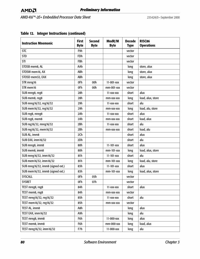
AMD-K6™-2E+ Embedded Processor Data Sheet 23542A/0—September 2000
Preliminary Information
STC F9h vector
STD FDh vector
STI FBh vector
STOSB mem8, AL AAh long store, alux
STOSW mem16, AX ABh long store, alux
STOSD mem32, EAX ABh long store, alux
STR mreg16 0Fh 00h 11-001-xxx vector
STR mem16 0Fh 00h mm-001-xxx vector
SUB mreg8, reg8 28h 11-xxx-xxx short alux
SUB mem8, reg8 28h mm-xxx-xxx long load, alux, store
SUB mreg16/32, reg16/32 29h 11-xxx-xxx short alu
SUB mem16/32, reg16/32 29h mm-xxx-xxx long load, alu, store
SUB reg8, mreg8 2Ah 11-xxx-xxx short alux
SUB reg8, mem8 2Ah mm-xxx-xxx short load, alux
SUB reg16/32, mreg16/32 2Bh 11-xxx-xxx short alu
SUB reg16/32, mem16/32 2Bh mm-xxx-xxx short load, alu
SUB AL, imm8 2Ch short alux
SUB EAX, imm16/32 2Dh short alu
SUB mreg8, imm8 80h 11-101-xxx short alux
SUB mem8, imm8 80h mm-101-xxx long load, alux, store
SUB mreg16/32, imm16/32 81h 11-101-xxx short alu
SUB mem16/32, imm16/32 81h mm-101-xxx long load, alu, store
SUB mreg16/32, imm8 (signed ext.) 83h 11-101-xxx short alux
SUB mem16/32, imm8 (signed ext.) 83h mm-101-xxx long load, alux, store
SYSCALL 0Fh 05h vector
SYSRET 0Fh 07h vector
TEST mreg8, reg8 84h 11-xxx-xxx short alux
TEST mem8, reg8 84h mm-xxx-xxx vector
TEST mreg16/32, reg16/32 85h 11-xxx-xxx short alu
TEST mem16/32, reg16/32 85h mm-xxx-xxx vector
TEST AL, imm8 A8h long alux
TEST EAX, imm16/32 A9h long alu
TEST mreg8, imm8 F6h 11-000-xxx long alux
TEST mem8, imm8 F6h mm-000-xxx long load, alux
TEST mreg16/32, imm16/32 F7h 11-000-xxx long alu
Table 12. Integer Instructions (continued)
Instruction Mnemonic First Byte
Second Byte
ModR/M Byte
DecodeType
RISC86Operations
80 Software Environment Chapter 3

23542A/0—September 2000 AMD-K6™-2E+ Embedded Processor Data Sheet
Preliminary Information
TEST mem16/32, imm16/32 F7h mm-000-xxx long load, alu
VERR mreg16 0Fh 00h 11-100-xxx vector
VERR mem16 0Fh 00h mm-100-xxx vector
VERW mreg16 0Fh 00h 11-101-xxx vector
VERW mem16 0Fh 00h mm-101-xxx vector
WAIT 9Bh vector
WBINVD 0Fh 09h vector
WRMSR 0Fh 30h vector
XADD mreg8, reg8 0Fh C0h 11-100-xxx vector
XADD mem8, reg8 0Fh C0h mm-100-xxx vector
XADD mreg16/32, reg16/32 0Fh C1h 11-101-xxx vector
XADD mem16/32, reg16/32 0Fh C1h mm-101-xxx vector
XCHG reg8, mreg8 86h 11-xxx-xxx vector
XCHG reg8, mem8 86h mm-xxx-xxx vector
XCHG reg16/32, mreg16/32 87h 11-xxx-xxx vector
XCHG reg16/32, mem16/32 87h mm-xxx-xxx vector
XCHG EAX, EAX 90h short limm
XCHG EAX, ECX 91h long alu, alu, alu
XCHG EAX, EDX 92h long alu, alu, alu
XCHG EAX, EBX 93h long alu, alu, alu
XCHG EAX, ESP 94h long alu, alu, alu
XCHG EAX, EBP 95h long alu, alu, alu
XCHG EAX, ESI 96h long alu, alu, alu
XCHG EAX, EDI 97h long alu, alu, alu
XLAT D7h vector
XOR mreg8, reg8 30h 11-xxx-xxx short alux
XOR mem8, reg8 30h mm-xxx-xxx long load, alux, store
XOR mreg16/32, reg16/32 31h 11-xxx-xxx short alu
XOR mem16/32, reg16/32 31h mm-xxx-xxx long load, alu, store
XOR reg8, mreg8 32h 11-xxx-xxx short alux
XOR reg8, mem8 32h mm-xxx-xxx short load, alux
XOR reg16/32, mreg16/32 33h 11-xxx-xxx short alu
XOR reg16/32, mem16/32 33h mm-xxx-xxx short load, alu
XOR AL, imm8 34h short alux
XOR EAX, imm16/32 35h short alu
Table 12. Integer Instructions (continued)
Instruction Mnemonic First Byte
Second Byte
ModR/M Byte
DecodeType
RISC86Operations
Chapter 3 Software Environment 81

AMD-K6™-2E+ Embedded Processor Data Sheet 23542A/0—September 2000
Preliminary Information
XOR mreg8, imm8 80h 11-110-xxx short alux
XOR mem8, imm8 80h mm-110-xxx long load, alux, store
XOR mreg16/32, imm16/32 81h 11-110-xxx short alu
XOR mem16/32, imm16/32 81h mm-110-xxx long load, alu, store
XOR mreg16/32, imm8 (signed ext.) 83h 11-110-xxx short alux
XOR mem16/32, imm8 (signed ext.) 83h mm-110-xxx long load, alux, store
Table 13. Floating-Point Instructions
Instruction Mnemonic First Byte
Second Byte
ModR/M Byte
DecodeType
RISC86Operations
F2XM1 D9h F0h short float
FABS D9h F1h short float
FADD ST(0), ST(i)1 D8h 11-000-xxx short float
FADD ST(0), mem32real D8h mm-000-xxx short fload, float
FADD ST(i), ST(0)1 DCh 11-000-xxx short float
FADD ST(0), mem64real DCh mm-000-xxx short fload, float
FADDP ST(i), ST(0)1 DEh 11-000-xxx short float
FBLD DFh mm-100-xxx vector
FBSTP DFh mm-110-xxx vector
FCHS D9h E0h short float
FCLEX DBh E2h vector
FCOM ST(0), ST(i)1 D8h 11-010-xxx short float
FCOM ST(0), mem32real D8h mm-010-xxx short fload, float
FCOM ST(0), mem64real DCh mm-010-xxx short fload, float
FCOMP ST(0), ST(i)1 D8h 11-011-xxx short float
FCOMP ST(0), mem32real D8h mm-011-xxx short fload, float
FCOMP ST(0), mem64real DCh mm-011-xxx short fload, float
FCOMPP DEh D9h 11-011-001 short float
FCOS D9h FFh short float
FDECSTP D9h F6h short float
FDIV ST(0), ST(i) (single precision)1 D8h 11-110-xxx short float
FDIV ST(0), ST(i) (double precision)1 D8h 11-110-xxx short float
FDIV ST(0), ST(i) (extended precision)1 D8h 11-110-xxx short float
Table 12. Integer Instructions (continued)
Instruction Mnemonic First Byte
Second Byte
ModR/M Byte
DecodeType
RISC86Operations
82 Software Environment Chapter 3
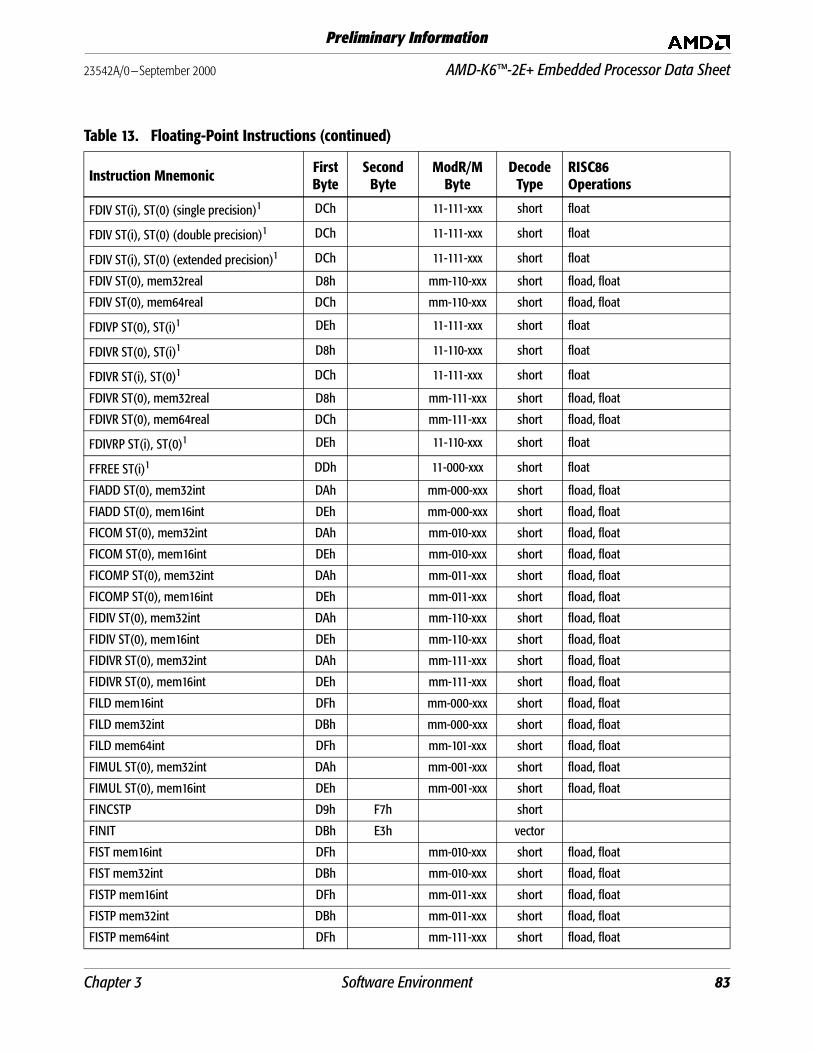
23542A/0—September 2000 AMD-K6™-2E+ Embedded Processor Data Sheet
Preliminary Information
FDIV ST(i), ST(0) (single precision)1 DCh 11-111-xxx short float
FDIV ST(i), ST(0) (double precision)1 DCh 11-111-xxx short float
FDIV ST(i), ST(0) (extended precision)1 DCh 11-111-xxx short float
FDIV ST(0), mem32real D8h mm-110-xxx short fload, float
FDIV ST(0), mem64real DCh mm-110-xxx short fload, float
FDIVP ST(0), ST(i)1 DEh 11-111-xxx short float
FDIVR ST(0), ST(i)1 D8h 11-110-xxx short float
FDIVR ST(i), ST(0)1 DCh 11-111-xxx short float
FDIVR ST(0), mem32real D8h mm-111-xxx short fload, float
FDIVR ST(0), mem64real DCh mm-111-xxx short fload, float
FDIVRP ST(i), ST(0)1 DEh 11-110-xxx short float
FFREE ST(i)1 DDh 11-000-xxx short float
FIADD ST(0), mem32int DAh mm-000-xxx short fload, float
FIADD ST(0), mem16int DEh mm-000-xxx short fload, float
FICOM ST(0), mem32int DAh mm-010-xxx short fload, float
FICOM ST(0), mem16int DEh mm-010-xxx short fload, float
FICOMP ST(0), mem32int DAh mm-011-xxx short fload, float
FICOMP ST(0), mem16int DEh mm-011-xxx short fload, float
FIDIV ST(0), mem32int DAh mm-110-xxx short fload, float
FIDIV ST(0), mem16int DEh mm-110-xxx short fload, float
FIDIVR ST(0), mem32int DAh mm-111-xxx short fload, float
FIDIVR ST(0), mem16int DEh mm-111-xxx short fload, float
FILD mem16int DFh mm-000-xxx short fload, float
FILD mem32int DBh mm-000-xxx short fload, float
FILD mem64int DFh mm-101-xxx short fload, float
FIMUL ST(0), mem32int DAh mm-001-xxx short fload, float
FIMUL ST(0), mem16int DEh mm-001-xxx short fload, float
FINCSTP D9h F7h short
FINIT DBh E3h vector
FIST mem16int DFh mm-010-xxx short fload, float
FIST mem32int DBh mm-010-xxx short fload, float
FISTP mem16int DFh mm-011-xxx short fload, float
FISTP mem32int DBh mm-011-xxx short fload, float
FISTP mem64int DFh mm-111-xxx short fload, float
Table 13. Floating-Point Instructions (continued)
Instruction Mnemonic First Byte
Second Byte
ModR/M Byte
DecodeType
RISC86Operations
Chapter 3 Software Environment 83
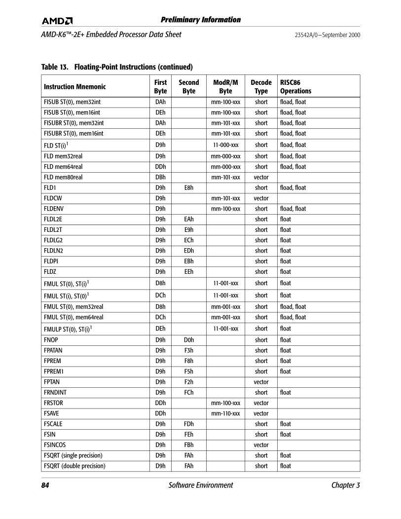
AMD-K6™-2E+ Embedded Processor Data Sheet 23542A/0—September 2000
Preliminary Information
FISUB ST(0), mem32int DAh mm-100-xxx short fload, float
FISUB ST(0), mem16int DEh mm-100-xxx short fload, float
FISUBR ST(0), mem32int DAh mm-101-xxx short fload, float
FISUBR ST(0), mem16int DEh mm-101-xxx short fload, float
FLD ST(i)1 D9h 11-000-xxx short fload, float
FLD mem32real D9h mm-000-xxx short fload, float
FLD mem64real DDh mm-000-xxx short fload, float
FLD mem80real DBh mm-101-xxx vector
FLD1 D9h E8h short fload, float
FLDCW D9h mm-101-xxx vector
FLDENV D9h mm-100-xxx short fload, float
FLDL2E D9h EAh short float
FLDL2T D9h E9h short float
FLDLG2 D9h ECh short float
FLDLN2 D9h EDh short float
FLDPI D9h EBh short float
FLDZ D9h EEh short float
FMUL ST(0), ST(i)1 D8h 11-001-xxx short float
FMUL ST(i), ST(0)1 DCh 11-001-xxx short float
FMUL ST(0), mem32real D8h mm-001-xxx short fload, float
FMUL ST(0), mem64real DCh mm-001-xxx short fload, float
FMULP ST(0), ST(i)1 DEh 11-001-xxx short float
FNOP D9h D0h short float
FPATAN D9h F3h short float
FPREM D9h F8h short float
FPREM1 D9h F5h short float
FPTAN D9h F2h vector
FRNDINT D9h FCh short float
FRSTOR DDh mm-100-xxx vector
FSAVE DDh mm-110-xxx vector
FSCALE D9h FDh short float
FSIN D9h FEh short float
FSINCOS D9h FBh vector
FSQRT (single precision) D9h FAh short float
FSQRT (double precision) D9h FAh short float
Table 13. Floating-Point Instructions (continued)
Instruction Mnemonic First Byte
Second Byte
ModR/M Byte
DecodeType
RISC86Operations
84 Software Environment Chapter 3
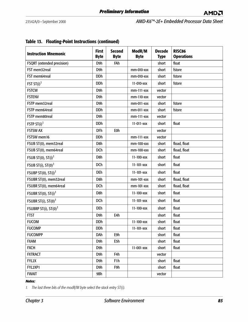
23542A/0—September 2000 AMD-K6™-2E+ Embedded Processor Data Sheet
Preliminary Information
FSQRT (extended precision) D9h FAh short float
FST mem32real D9h mm-010-xxx short fstore
FST mem64real DDh mm-010-xxx short fstore
FST ST(i)1 DDh 11-010-xxx short fstore
FSTCW D9h mm-111-xxx vector
FSTENV D9h mm-110-xxx vector
FSTP mem32real D9h mm-011-xxx short fstore
FSTP mem64real DDh mm-011-xxx short fstore
FSTP mem80real D9h mm-111-xxx vector
FSTP ST(i)1 DDh 11-011-xxx short float
FSTSW AX DFh E0h vector
FSTSW mem16 DDh mm-111-xxx vector
FSUB ST(0), mem32real D8h mm-100-xxx short fload, float
FSUB ST(0), mem64real DCh mm-100-xxx short fload, float
FSUB ST(0), ST(i)1 D8h 11-100-xxx short float
FSUB ST(i), ST(0)1 DCh 11-101-xxx short float
FSUBP ST(0), ST(i)1 DEh 11-101-xxx short float
FSUBR ST(0), mem32real D8h mm-101-xxx short fload, float
FSUBR ST(0), mem64real DCh mm-101-xxx short fload, float
FSUBR ST(0), ST(i)1 D8h 11-100-xxx short float
FSUBR ST(i), ST(0)1 DCh 11-101-xxx short float
FSUBRP ST(i), ST(0)1 DEh 11-100-xxx short float
FTST D9h E4h short float
FUCOM DDh 11-100-xxx short float
FUCOMP DDh 11-101-xxx short float
FUCOMPP DAh E9h short float
FXAM D9h E5h short float
FXCH D9h 11-001-xxx short float
FXTRACT D9h F4h vector
FYL2X D9h F1h short float
FYL2XP1 D9h F9h short float
FWAIT 9Bh vector
Notes:
1. The last three bits of the modR/M byte select the stack entry ST(i).
Table 13. Floating-Point Instructions (continued)
Instruction Mnemonic First Byte
Second Byte
ModR/M Byte
DecodeType
RISC86Operations
Chapter 3 Software Environment 85
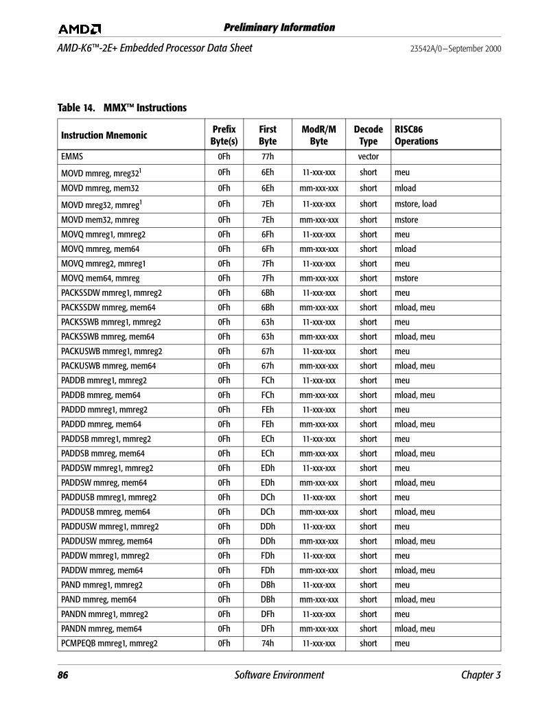
AMD-K6™-2E+ Embedded Processor Data Sheet 23542A/0—September 2000
Preliminary Information
Table 14. MMX™ Instructions
Instruction Mnemonic PrefixByte(s)
FirstByte
ModR/M Byte
DecodeType
RISC86Operations
EMMS 0Fh 77h vector
MOVD mmreg, mreg321 0Fh 6Eh 11-xxx-xxx short meu
MOVD mmreg, mem32 0Fh 6Eh mm-xxx-xxx short mload
MOVD mreg32, mmreg1 0Fh 7Eh 11-xxx-xxx short mstore, load
MOVD mem32, mmreg 0Fh 7Eh mm-xxx-xxx short mstore
MOVQ mmreg1, mmreg2 0Fh 6Fh 11-xxx-xxx short meu
MOVQ mmreg, mem64 0Fh 6Fh mm-xxx-xxx short mload
MOVQ mmreg2, mmreg1 0Fh 7Fh 11-xxx-xxx short meu
MOVQ mem64, mmreg 0Fh 7Fh mm-xxx-xxx short mstore
PACKSSDW mmreg1, mmreg2 0Fh 6Bh 11-xxx-xxx short meu
PACKSSDW mmreg, mem64 0Fh 6Bh mm-xxx-xxx short mload, meu
PACKSSWB mmreg1, mmreg2 0Fh 63h 11-xxx-xxx short meu
PACKSSWB mmreg, mem64 0Fh 63h mm-xxx-xxx short mload, meu
PACKUSWB mmreg1, mmreg2 0Fh 67h 11-xxx-xxx short meu
PACKUSWB mmreg, mem64 0Fh 67h mm-xxx-xxx short mload, meu
PADDB mmreg1, mmreg2 0Fh FCh 11-xxx-xxx short meu
PADDB mmreg, mem64 0Fh FCh mm-xxx-xxx short mload, meu
PADDD mmreg1, mmreg2 0Fh FEh 11-xxx-xxx short meu
PADDD mmreg, mem64 0Fh FEh mm-xxx-xxx short mload, meu
PADDSB mmreg1, mmreg2 0Fh ECh 11-xxx-xxx short meu
PADDSB mmreg, mem64 0Fh ECh mm-xxx-xxx short mload, meu
PADDSW mmreg1, mmreg2 0Fh EDh 11-xxx-xxx short meu
PADDSW mmreg, mem64 0Fh EDh mm-xxx-xxx short mload, meu
PADDUSB mmreg1, mmreg2 0Fh DCh 11-xxx-xxx short meu
PADDUSB mmreg, mem64 0Fh DCh mm-xxx-xxx short mload, meu
PADDUSW mmreg1, mmreg2 0Fh DDh 11-xxx-xxx short meu
PADDUSW mmreg, mem64 0Fh DDh mm-xxx-xxx short mload, meu
PADDW mmreg1, mmreg2 0Fh FDh 11-xxx-xxx short meu
PADDW mmreg, mem64 0Fh FDh mm-xxx-xxx short mload, meu
PAND mmreg1, mmreg2 0Fh DBh 11-xxx-xxx short meu
PAND mmreg, mem64 0Fh DBh mm-xxx-xxx short mload, meu
PANDN mmreg1, mmreg2 0Fh DFh 11-xxx-xxx short meu
PANDN mmreg, mem64 0Fh DFh mm-xxx-xxx short mload, meu
PCMPEQB mmreg1, mmreg2 0Fh 74h 11-xxx-xxx short meu
86 Software Environment Chapter 3

23542A/0—September 2000 AMD-K6™-2E+ Embedded Processor Data Sheet
Preliminary Information
PCMPEQB mmreg, mem64 0Fh 74h mm-xxx-xxx short mload, meu
PCMPEQD mmreg1, mmreg2 0Fh 76h 11-xxx-xxx short meu
PCMPEQD mmreg, mem64 0Fh 76h mm-xxx-xxx short mload, meu
PCMPEQW mmreg1, mmreg2 0Fh 75h 11-xxx-xxx short meu
PCMPEQW mmreg, mem64 0Fh 75h mm-xxx-xxx short mload, meu
PCMPGTB mmreg1, mmreg2 0Fh 64h 11-xxx-xxx short meu
PCMPGTB mmreg, mem64 0Fh 64h mm-xxx-xxx short mload, meu
PCMPGTD mmreg1, mmreg2 0Fh 66h 11-xxx-xxx short meu
PCMPGTD mmreg, mem64 0Fh 66h mm-xxx-xxx short mload, meu
PCMPGTW mmreg1, mmreg2 0Fh 65h 11-xxx-xxx short meu
PCMPGTW mmreg, mem64 0Fh 65h mm-xxx-xxx short mload, meu
PMADDWD mmreg1, mmreg2 0Fh F5h 11-xxx-xxx short meu
PMADDWD mmreg, mem64 0Fh F5h mm-xxx-xxx short mload, meu
PMULHW mmreg1, mmreg2 0Fh E5h 11-xxx-xxx short meu
PMULHW mmreg, mem64 0Fh E5h mm-xxx-xxx short mload, meu
PMULLW mmreg1, mmreg2 0Fh D5h 11-xxx-xxx short meu
PMULLW mmreg, mem64 0Fh D5h mm-xxx-xxx short mload, meu
POR mmreg1, mmreg2 0Fh EBh 11-xxx-xxx short meu
POR mmreg, mem64 0Fh EBh mm-xxx-xxx short mload, meu
PSLLD mmreg1, mmreg2 0Fh F2h 11-xxx-xxx short meu
PSLLD mmreg, mem64 0Fh F2h mm-xxx-xxx short mload, meu
PSLLD mmreg, imm8 0Fh 72h 11-110-xxx short meu
PSLLQ mmreg1, mmreg2 0Fh F3h 11-xxx-xxx short meu
PSLLQ mmreg, mem64 0Fh F3h mm-xxx-xxx short mload, meu
PSLLQ mmreg, imm8 0Fh 73h 11-110-xxx short meu
PSLLW mmreg1, mmreg2 0Fh F1h 11-xxx-xxx short meu
PSLLW mmreg, mem64 0Fh F1h mm-xxx-xxx short mload, meu
PSLLW mmreg, imm8 0Fh 71h 11-110-xxx short meu
PSRAD mmreg1, mmreg2 0Fh E2h 11-xxx-xxx short meu
PSRAD mmreg, mem64 0Fh E2h mm-xxx-xxx short mload, meu
PSRAD mmreg, imm8 0Fh 72h 11-100-xxx short meu
PSRAW mmreg1, mmreg2 0Fh E1h 11-xxx-xxx short meu
PSRAW mmreg, mem64 0Fh E1h mm-xxx-xxx short mload, meu
PSRAW mmreg, imm8 0Fh 71h 11-100-xxx short meu
PSRLD mmreg1, mmreg2 0Fh D2h 11-xxx-xxx short meu
Table 14. MMX™ Instructions (continued)
Instruction Mnemonic PrefixByte(s)
FirstByte
ModR/M Byte
DecodeType
RISC86Operations
Chapter 3 Software Environment 87
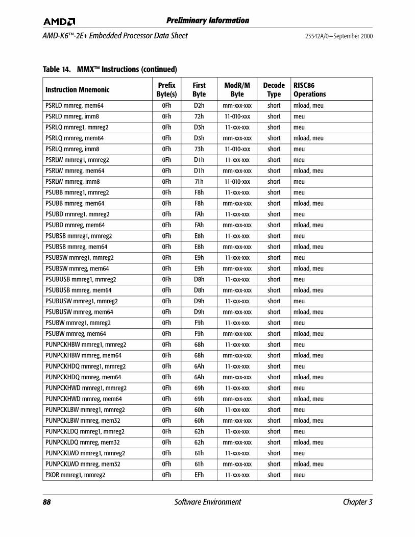
AMD-K6™-2E+ Embedded Processor Data Sheet 23542A/0—September 2000
Preliminary Information
PSRLD mmreg, mem64 0Fh D2h mm-xxx-xxx short mload, meu
PSRLD mmreg, imm8 0Fh 72h 11-010-xxx short meu
PSRLQ mmreg1, mmreg2 0Fh D3h 11-xxx-xxx short meu
PSRLQ mmreg, mem64 0Fh D3h mm-xxx-xxx short mload, meu
PSRLQ mmreg, imm8 0Fh 73h 11-010-xxx short meu
PSRLW mmreg1, mmreg2 0Fh D1h 11-xxx-xxx short meu
PSRLW mmreg, mem64 0Fh D1h mm-xxx-xxx short mload, meu
PSRLW mmreg, imm8 0Fh 71h 11-010-xxx short meu
PSUBB mmreg1, mmreg2 0Fh F8h 11-xxx-xxx short meu
PSUBB mmreg, mem64 0Fh F8h mm-xxx-xxx short mload, meu
PSUBD mmreg1, mmreg2 0Fh FAh 11-xxx-xxx short meu
PSUBD mmreg, mem64 0Fh FAh mm-xxx-xxx short mload, meu
PSUBSB mmreg1, mmreg2 0Fh E8h 11-xxx-xxx short meu
PSUBSB mmreg, mem64 0Fh E8h mm-xxx-xxx short mload, meu
PSUBSW mmreg1, mmreg2 0Fh E9h 11-xxx-xxx short meu
PSUBSW mmreg, mem64 0Fh E9h mm-xxx-xxx short mload, meu
PSUBUSB mmreg1, mmreg2 0Fh D8h 11-xxx-xxx short meu
PSUBUSB mmreg, mem64 0Fh D8h mm-xxx-xxx short mload, meu
PSUBUSW mmreg1, mmreg2 0Fh D9h 11-xxx-xxx short meu
PSUBUSW mmreg, mem64 0Fh D9h mm-xxx-xxx short mload, meu
PSUBW mmreg1, mmreg2 0Fh F9h 11-xxx-xxx short meu
PSUBW mmreg, mem64 0Fh F9h mm-xxx-xxx short mload, meu
PUNPCKHBW mmreg1, mmreg2 0Fh 68h 11-xxx-xxx short meu
PUNPCKHBW mmreg, mem64 0Fh 68h mm-xxx-xxx short mload, meu
PUNPCKHDQ mmreg1, mmreg2 0Fh 6Ah 11-xxx-xxx short meu
PUNPCKHDQ mmreg, mem64 0Fh 6Ah mm-xxx-xxx short mload, meu
PUNPCKHWD mmreg1, mmreg2 0Fh 69h 11-xxx-xxx short meu
PUNPCKHWD mmreg, mem64 0Fh 69h mm-xxx-xxx short mload, meu
PUNPCKLBW mmreg1, mmreg2 0Fh 60h 11-xxx-xxx short meu
PUNPCKLBW mmreg, mem32 0Fh 60h mm-xxx-xxx short mload, meu
PUNPCKLDQ mmreg1, mmreg2 0Fh 62h 11-xxx-xxx short meu
PUNPCKLDQ mmreg, mem32 0Fh 62h mm-xxx-xxx short mload, meu
PUNPCKLWD mmreg1, mmreg2 0Fh 61h 11-xxx-xxx short meu
PUNPCKLWD mmreg, mem32 0Fh 61h mm-xxx-xxx short mload, meu
PXOR mmreg1, mmreg2 0Fh EFh 11-xxx-xxx short meu
Table 14. MMX™ Instructions (continued)
Instruction Mnemonic PrefixByte(s)
FirstByte
ModR/M Byte
DecodeType
RISC86Operations
88 Software Environment Chapter 3
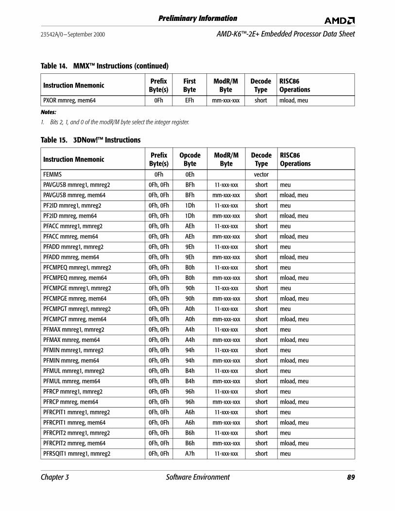
23542A/0—September 2000 AMD-K6™-2E+ Embedded Processor Data Sheet
Preliminary Information
PXOR mmreg, mem64 0Fh EFh mm-xxx-xxx short mload, meu
Notes:
1. Bits 2, 1, and 0 of the modR/M byte select the integer register.
Table 15. 3DNow!™ Instructions
Instruction Mnemonic PrefixByte(s)
OpcodeByte
ModR/M Byte
DecodeType
RISC86Operations
FEMMS 0Fh 0Eh vector
PAVGUSB mmreg1, mmreg2 0Fh, 0Fh BFh 11-xxx-xxx short meu
PAVGUSB mmreg, mem64 0Fh, 0Fh BFh mm-xxx-xxx short mload, meu
PF2ID mmreg1, mmreg2 0Fh, 0Fh 1Dh 11-xxx-xxx short meu
PF2ID mmreg, mem64 0Fh, 0Fh 1Dh mm-xxx-xxx short mload, meu
PFACC mmreg1, mmreg2 0Fh, 0Fh AEh 11-xxx-xxx short meu
PFACC mmreg, mem64 0Fh, 0Fh AEh mm-xxx-xxx short mload, meu
PFADD mmreg1, mmreg2 0Fh, 0Fh 9Eh 11-xxx-xxx short meu
PFADD mmreg, mem64 0Fh, 0Fh 9Eh mm-xxx-xxx short mload, meu
PFCMPEQ mmreg1, mmreg2 0Fh, 0Fh B0h 11-xxx-xxx short meu
PFCMPEQ mmreg, mem64 0Fh, 0Fh B0h mm-xxx-xxx short mload, meu
PFCMPGE mmreg1, mmreg2 0Fh, 0Fh 90h 11-xxx-xxx short meu
PFCMPGE mmreg, mem64 0Fh, 0Fh 90h mm-xxx-xxx short mload, meu
PFCMPGT mmreg1, mmreg2 0Fh, 0Fh A0h 11-xxx-xxx short meu
PFCMPGT mmreg, mem64 0Fh, 0Fh A0h mm-xxx-xxx short mload, meu
PFMAX mmreg1, mmreg2 0Fh, 0Fh A4h 11-xxx-xxx short meu
PFMAX mmreg, mem64 0Fh, 0Fh A4h mm-xxx-xxx short mload, meu
PFMIN mmreg1, mmreg2 0Fh, 0Fh 94h 11-xxx-xxx short meu
PFMIN mmreg, mem64 0Fh, 0Fh 94h mm-xxx-xxx short mload, meu
PFMUL mmreg1, mmreg2 0Fh, 0Fh B4h 11-xxx-xxx short meu
PFMUL mmreg, mem64 0Fh, 0Fh B4h mm-xxx-xxx short mload, meu
PFRCP mmreg1, mmreg2 0Fh, 0Fh 96h 11-xxx-xxx short meu
PFRCP mmreg, mem64 0Fh, 0Fh 96h mm-xxx-xxx short mload, meu
PFRCPIT1 mmreg1, mmreg2 0Fh, 0Fh A6h 11-xxx-xxx short meu
PFRCPIT1 mmreg, mem64 0Fh, 0Fh A6h mm-xxx-xxx short mload, meu
PFRCPIT2 mmreg1, mmreg2 0Fh, 0Fh B6h 11-xxx-xxx short meu
PFRCPIT2 mmreg, mem64 0Fh, 0Fh B6h mm-xxx-xxx short mload, meu
PFRSQIT1 mmreg1, mmreg2 0Fh, 0Fh A7h 11-xxx-xxx short meu
Table 14. MMX™ Instructions (continued)
Instruction Mnemonic PrefixByte(s)
FirstByte
ModR/M Byte
DecodeType
RISC86Operations
Chapter 3 Software Environment 89
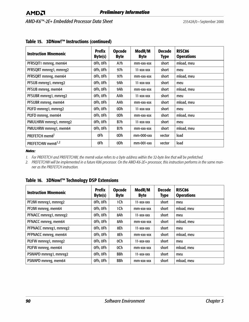
AMD-K6™-2E+ Embedded Processor Data Sheet 23542A/0—September 2000
Preliminary Information
PFRSQIT1 mmreg, mem64 0Fh, 0Fh A7h mm-xxx-xxx short mload, meu
PFRSQRT mmreg1, mmreg2 0Fh, 0Fh 97h 11-xxx-xxx short meu
PFRSQRT mmreg, mem64 0Fh, 0Fh 97h mm-xxx-xxx short mload, meu
PFSUB mmreg1, mmreg2 0Fh, 0Fh 9Ah 11-xxx-xxx short meu
PFSUB mmreg, mem64 0Fh, 0Fh 9Ah mm-xxx-xxx short mload, meu
PFSUBR mmreg1, mmreg2 0Fh, 0Fh AAh 11-xxx-xxx short meu
PFSUBR mmreg, mem64 0Fh, 0Fh AAh mm-xxx-xxx short mload, meu
PI2FD mmreg1, mmreg2 0Fh, 0Fh 0Dh 11-xxx-xxx short meu
PI2FD mmreg, mem64 0Fh, 0Fh 0Dh mm-xxx-xxx short mload, meu
PMULHRW mmreg1, mmreg2 0Fh, 0Fh B7h 11-xxx-xxx short meu
PMULHRW mmreg1, mem64 0Fh, 0Fh B7h mm-xxx-xxx short mload, meu
PREFETCH mem81 0Fh 0Dh mm-000-xxx vector load
PREFETCHW mem81,2 0Fh 0Dh mm-001-xxx vector load
Notes:
1. For PREFETCH and PREFETCHW, the mem8 value refers to a byte address within the 32-byte line that will be prefetched.2. PREFETCHW will be implemented in a future K86 processor. On the AMD-K6-2E+ processor, this instruction performs in the same man-
ner as the PREFETCH instruction.
Table 16. 3DNow!™ Technology DSP Extensions
Instruction Mnemonic PrefixByte(s)
OpcodeByte
ModR/M Byte
DecodeType
RISC86Operations
PF2IW mmreg1, mmreg2 0Fh, 0Fh 1Ch 11-xxx-xxx short meu
PF2IW mmreg, mem64 0Fh, 0Fh 1Ch mm-xxx-xxx short mload, meu
PFNACC mmreg1, mmreg2 0Fh, 0Fh 8Ah 11-xxx-xxx short meu
PFNACC mmreg, mem64 0Fh, 0Fh 8Ah mm-xxx-xxx short mload, meu
PFPNACC mmreg1, mmreg2 0Fh, 0Fh 8Eh 11-xxx-xxx short meu
PFPNACC mmreg, mem64 0Fh, 0Fh 8Eh mm-xxx-xxx short mload, meu
PI2FW mmreg1, mmreg2 0Fh, 0Fh 0Ch 11-xxx-xxx short meu
PI2FW mmreg, mem64 0Fh, 0Fh 0Ch mm-xxx-xxx short mload, meu
PSWAPD mmreg1, mmreg2 0Fh, 0Fh BBh 11-xxx-xxx short meu
PSWAPD mmreg, mem64 0Fh, 0Fh BBh mm-xxx-xxx short mload, meu
Table 15. 3DNow!™ Instructions (continued)
Instruction Mnemonic PrefixByte(s)
OpcodeByte
ModR/M Byte
DecodeType
RISC86Operations
90 Software Environment Chapter 3
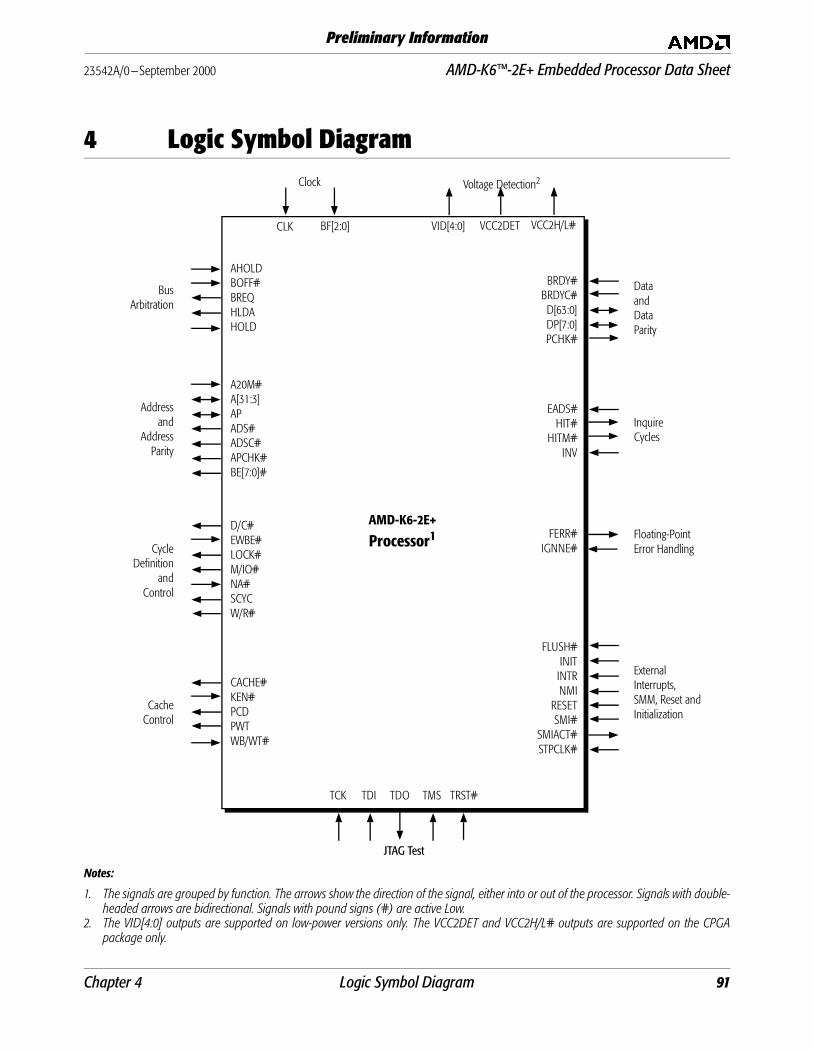
23542A/0—September 2000 AMD-K6™-2E+ Embedded Processor Data Sheet
Preliminary Information
4 Logic Symbol Diagram
Notes:
1. The signals are grouped by function. The arrows show the direction of the signal, either into or out of the processor. Signals with double-headed arrows are bidirectional. Signals with pound signs (#) are active Low.
2. The VID[4:0] outputs are supported on low-power versions only. The VCC2DET and VCC2H/L# outputs are supported on the CPGApackage only.
A20M#A[31:3]APADS#ADSC#APCHK#BE[7:0]#
AHOLDBOFF#BREQHLDAHOLD
D/C#EWBE#LOCK#M/IO#NA#SCYCW/R#
CACHE#KEN#PCDPWTWB/WT#
Clock
BusArbitration
CLK BF[2:0]
TCK TDI TDO TMS TRST#
BRDY#BRDYC#D[63:0]DP[7:0]PCHK#
EADS#HIT#
HITM#INV
FERR#IGNNE#
FLUSH#INIT
INTRNMI
RESETSMI#
SMIACT#STPCLK#
JTAG Test
DataandData Parity
InquireCycles
Floating-PointError Handling
ExternalInterrupts,SMM, Reset and Initialization
Addressand
AddressParity
CycleDefinition
andControl
CacheControl
AMD-K6-2E+
Processor1
Voltage Detection2
VCC2DET VCC2H/L#VID[4:0]
Chapter 4 Logic Symbol Diagram 91
AMD-K6™-2E+ Embedded Processor Data Sheet 23542A/0—September 2000
Preliminary Information
92 Logic Symbol Diagram Chapter 4
23542A/0—September 2000 AMD-K6™-2E+ Embedded Processor Data Sheet
Preliminary Information
5 Signal Descriptions
This chapter includes a detailed description of each signalsupported on the AMD-K6-2E+ processor. This chapter alsoprovides tables listing the signals grouped by type, beginningon page 140.
The logic symbol diagram on page 91 shows the signals groupedby function.
Connection diagrams and pins listed by high-level function areincluded in Chapter 18, “Pin Designations” on page 321.
5.1 Signal Terminology
The following terminology is used in this chapter:
■ Driven—The processor actively pulls the signal up to theHigh-voltage state or pulls the signal down to theLow-voltage state.
■ Floated—The signal is not being driven by the processor(high-impedance state), which allows another device todrive this signal.
■ Asserted—For all active High signals, the term assertedmeans the signal is in the High-voltage state. For all activeLow signals, the term asserted means the signal is in theLow-voltage state. See Table 19 on page 140 for informationon asserting signals synchronously and asynchronously.
■ Negated—For all active High signals, the term negated meansthe signal is in the Low-voltage state. For all active Lowsignals, the term negated means the signal is in theHigh-voltage state.
■ Sampled—The processor has measured the state of a signalat predefined points in time and will take the appropriateaction based on the state of the signal. If a signal is notsampled by the processor, its assertion or negation has noeffect on the operation of the processor.
Chapter 5 Signal Descriptions 93
AMD-K6™-2E+ Embedded Processor Data Sheet 23542A/0—September 2000
Preliminary Information
5.2 A20M# (Address Bit 20 Mask)
Pin Attribute Input
Summary A20M# is used to simulate the behavior of the 8086 whenrunning in Real mode. The assertion of A20M# causes theprocessor to force bit 20 of the physical address to 0 prior toaccessing the caches or driving out a memory bus cycle. Theclearing of address bit 20 maps addresses that extend above the8086 1-Mbyte limit to below 1 Mbyte.
Sampled The processor samples A20M# as a level-sensitive input onevery clock edge. The system logic can drive the signal eithersynchronously or asynchronously. I f i t i s assertedasynchronously, it must be asserted for a minimum pulse widthof two clocks.
The following list explains the effects of the processor samplingA20M# asserted under various conditions:
■ Inquire cycles and writeback cycles are not affected by thestate of A20M#.
■ The assertion of A20M# in System Management Mode(SMM) is ignored.
■ When A20M# is sampled asserted in Protected mode, itcauses unpredictable processor operation. A20M# is onlydefined in Real mode.
■ To ensure that A20M# is recognized before the first ADS#occurs following the negation of RESET, A20M# must besampled asserted on the same clock edge that RESET issampled negated or on one of the two subsequent clockedges.
■ To ensure A20M# is recognized before the execution of aninstruction, a serializing instruction must be executedbetween the instruction that asserts A20M# and thetargeted instruction. (A serializing instruction is aninstruction inserted between operations to enforce programorder. It forces the processor to finish all modifications toflags, registers, and memory before the next instruction isexecuted.)
94 Signal Descriptions Chapter 5
23542A/0—September 2000 AMD-K6™-2E+ Embedded Processor Data Sheet
Preliminary Information
5.3 A[31:3] (Address Bus)
Pin Attribute A[31:5] Bidirectional, A[4:3] Output
Summary A[31:3] contain the physical address for the current bus cycle.The processor drives addresses on A[31:3] during memory andI/O cycles, and cycle definition information during special buscycles. The processor samples addresses on A[31:5] duringinquire cycles.
Driven, Sampled, and Floated
As Outputs: A[31:3] are driven valid off the same clock edge asADS# and remain in the same state until the clock edge onwhich NA# or the last expected BRDY# of the cycle is sampledasserted. A[31:3] are driven during memory cycles, I/O cycles,special bus cycles, and interrupt acknowledge cycles. Theprocessor continues to drive the address bus while the bus isidle.
As Inputs: The processor samples A[31:5] during inquire cycleson the clock edge on which EADS# is sampled asserted. Eventhough A4 and A3 are not used during the inquire cycle, theymust be driven to a valid state and must meet the same timingsas A[31:5].
A[31:3] are floated off the clock edge that AHOLD or BOFF# issampled asserted and off the clock edge that the processorasserts HLDA in recognition of HOLD.
The processor resumes driving A[31:3] off the clock edge onwhich the processor samples AHOLD or BOFF# negated and offthe clock edge on which the processor negates HLDA.
Chapter 5 Signal Descriptions 95

AMD-K6™-2E+ Embedded Processor Data Sheet 23542A/0—September 2000
Preliminary Information
5.4 ADS# (Address Strobe)
Pin Attribute Output
Summary The assertion of ADS# indicates the beginning of a new buscycle. The address bus and all cycle definition signalscorresponding to this bus cycle are driven valid off the sameclock edge as ADS#.
Driven and Floated ADS# is asserted for one clock at the beginning of each buscycle. For non-pipelined cycles, ADS# can be asserted as earlyas the clock edge after the clock edge on which the lastexpected BRDY# of the cycle is sampled asserted, resulting in asingle idle state between cycles. For pipelined cycles if theprocessor is prepared to start a new cycle, ADS# can be assertedas early as one clock edge after NA# is sampled asserted.
If AHOLD is sampled asserted, ADS# is only driven in order toperform a writeback cycle due to an inquire cycle that hits amodified cache line.
The processor floats ADS# off the clock edge that BOFF# issampled asserted and off the clock edge that the processorasserts HLDA in recognition of HOLD.
5.5 ADSC# (Address Strobe Copy)
Pin Attribute Output
Summary ADSC# has the identical function and timing as ADS#. In theevent ADS# becomes too heavily loaded due to a large fanout ina system, ADSC# can be used to split the load across twooutputs, which can improve system timing.
96 Signal Descriptions Chapter 5
23542A/0—September 2000 AMD-K6™-2E+ Embedded Processor Data Sheet
Preliminary Information
5.6 AHOLD (Address Hold)
Pin Attribute Input
Summary AHOLD can be asserted by the system to initiate one or moreinquire cycles. To allow the system to drive the address busduring an inquire cycle, the processor floats A[31:3] and AP offthe clock edge on which AHOLD is sampled asserted. The databus and all other control and status signals remain under thecontrol of the processor and are not floated. This allows a buscycle that is in progress when AHOLD is sampled asserted tocontinue to completion. The processor resumes driving theaddress bus off the clock edge on which AHOLD is samplednegated.
If AHOLD is sampled asserted, ADS# is only asserted in orderto perform a writeback cycle due to an inquire cycle that hits amodified cache line.
Sampled The processor samples AHOLD on every clock edge. AHOLD isrecognized while INIT and RESET are sampled asserted.
Chapter 5 Signal Descriptions 97
AMD-K6™-2E+ Embedded Processor Data Sheet 23542A/0—September 2000
Preliminary Information
5.7 AP (Address Parity)
Pin Attribute Bidirectional
Summary AP contains the even parity bit for cache line addresses drivenand sampled on A[31:5]. Even parity means that the totalnumber of 1 bits on AP and A[31:5] is even. (A4 and A3 are notused for the generation or checking of address parity becausethese bits are not required to address a cache line.) AP is drivenby the processor during processor-initiated cycles and issampled by the processor during inquire cycles. If AP does notreflect even parity during an inquire cycle, the processorasserts APCHK# to indicate an address bus parity check. Theprocessor does not take an internal exception as the result ofdetecting an address bus parity check, and system logic mustrespond appropriately to the assertion of this signal.
Driven, Sampled, and Floated
As an Output: The processor drives AP valid off the clock edgeon which ADS# is asserted until the clock edge on which NA# orthe last expected BRDY# of the cycle is sampled asserted. AP isdriven during memory cycles, I/O cycles, special bus cycles, andinterrupt acknowledge cycles. The processor continues to driveAP while the bus is idle.
As an Input: The processor samples AP during inquire cycles onthe clock edge on which EADS# is sampled asserted.
The processor floats AP off the clock edge that AHOLD orBOFF# is sampled asserted and off the clock edge that theprocessor asserts HLDA in recognition of HOLD.
The processor resumes driving AP off the clock edge on whichthe processor samples AHOLD or BOFF# negated and off theclock edge on which the processor negates HLDA.
98 Signal Descriptions Chapter 5
23542A/0—September 2000 AMD-K6™-2E+ Embedded Processor Data Sheet
Preliminary Information
5.8 APCHK# (Address Parity Check)
Pin Attribute Output
Summary If the processor detects an address parity error during aninquire cycle, APCHK# is asserted for one clock. The processordoes not take an internal exception as the result of detecting anaddress bus parity check, and system logic must respondappropriately to the assertion of this signal.
The processor is designed so that APCHK# does not glitch,enabling the signal to be used as a clocking source for systemlogic.
Driven APCHK# is driven valid off the clock edge after the clock edgeon which the processor samples EADS# asserted. It is negatedoff the next clock edge.
APCHK# is always driven except in the Three-State Test mode.
Chapter 5 Signal Descriptions 99

AMD-K6™-2E+ Embedded Processor Data Sheet 23542A/0—September 2000
Preliminary Information
5.9 BE[7:0]# (Byte Enables)
Pin Attribute Output
Summary BE[7:0]# are used by the processor to indicate the valid databytes during a write cycle and the requested data bytes duringa read cycle. The byte enables can be used to derive address bitsA[2:0], which are not physically part of the processor’s addressbus. The processor checks and generates valid data parity forthe data bytes that are valid as defined by the byte enables. Theeight byte enables correspond to the eight bytes of the data busas follows:
The processor expects data to be driven by the system logic onall eight bytes of the data bus during a burst cache-line readcycle, independent of the byte enables that are asserted.
The byte enables are also used to distinguish between specialbus cycles as defined in Table 24 on page 142.
Driven and Floated BE[7:0]# are driven off the same clock edge as ADS# andremain in the same state until the clock edge on which NA# orthe last expected BRDY# of the cycle is sampled asserted.BE[7:0]# are driven during memory cycles, I/O cycles, specialbus cycles, and interrupt acknowledge cycles.
The processor floats BE[7:0]# off the clock edge that BOFF# issampled asserted and off the clock edge that the processorasserts HLDA in recognition of HOLD. Unlike the address bus,BE[7:0]# are not floated in response to AHOLD.
■ BE7#: D[63:56] ■ BE3#: D[31:24]■ BE6#: D[55:48] ■ BE2#: D[23:16]■ BE5#: D[47:40] ■ BE1#: D[15:8]■ BE4#: D[39:32] ■ BE0#: D[7:0]
100 Signal Descriptions Chapter 5
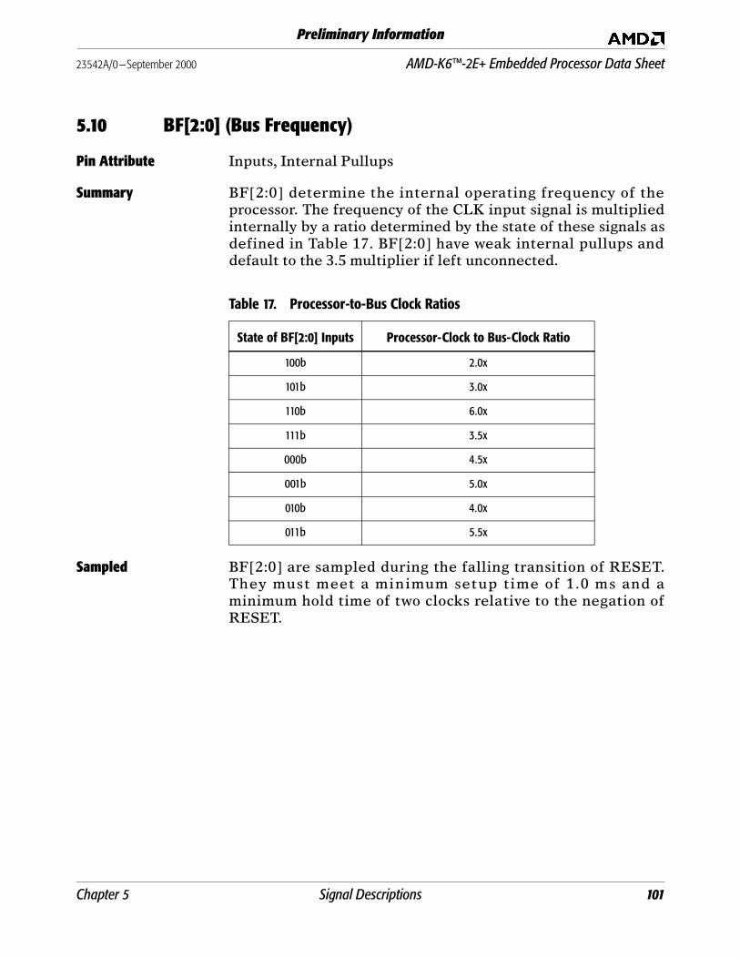
23542A/0—September 2000 AMD-K6™-2E+ Embedded Processor Data Sheet
Preliminary Information
5.10 BF[2:0] (Bus Frequency)
Pin Attribute Inputs, Internal Pullups
Summary BF[2:0] determine the internal operating frequency of theprocessor. The frequency of the CLK input signal is multipliedinternally by a ratio determined by the state of these signals asdefined in Table 17. BF[2:0] have weak internal pullups anddefault to the 3.5 multiplier if left unconnected.
Sampled BF[2:0] are sampled during the falling transition of RESET.They must meet a minimum setup time of 1.0 ms and aminimum hold time of two clocks relative to the negation ofRESET.
Table 17. Processor-to-Bus Clock Ratios
State of BF[2:0] Inputs Processor-Clock to Bus-Clock Ratio
100b 2.0x
101b 3.0x
110b 6.0x
111b 3.5x
000b 4.5x
001b 5.0x
010b 4.0x
011b 5.5x
Chapter 5 Signal Descriptions 101
AMD-K6™-2E+ Embedded Processor Data Sheet 23542A/0—September 2000
Preliminary Information
5.11 BOFF# (Backoff)
Pin Attribute Input
Summary If BOFF# is sampled asserted, the processor unconditionallyaborts any cycles in progress and transitions to a bus hold stateby floating the following signals: A[31:3], ADS#, ADSC#, AP,BE[7:0]#, CACHE#, D[63:0], D/C#, DP[7:0], LOCK#, M/IO#,PCD, PWT, SCYC, and W/R#. These signals remain floated untilBOFF# is sampled negated. This allows an alternate bus masteror the system to control the bus.
When BOFF# is sampled negated, any processor cycle that wasaborted due to the assertion of BOFF# is restarted from thebeginning of the cycle, regardless of the number of transfersthat were completed. If BOFF# is sampled asserted on the sameclock edge as BRDY# of a bus cycle of any length, then BOFF#takes precedence over the BRDY#. In this case, the cycle isaborted and restarted after BOFF# is sampled negated.
Sampled BOFF# is sampled on every clock edge. The processor floats itsbus signals off the clock edge on which BOFF# is sampledasserted. These signals remain floated until the clock edge onwhich BOFF# is sampled negated.
BOFF # is recognized while INIT and RESET are sampledasserted.
102 Signal Descriptions Chapter 5
23542A/0—September 2000 AMD-K6™-2E+ Embedded Processor Data Sheet
Preliminary Information
5.12 BRDY# (Burst Ready)
Pin Attribute Input, Internal Pullup
Summary BRDY# is asserted to the processor by system logic to indicateeither that the data bus is being driven with valid data during aread cycle or that the data bus has been latched during a writecycle. If necessary, the system logic can insert bus cycle waitstates by negating BRDY# until it is ready to continue the datatransfer. BRDY# is also used to indicate the completion ofspecial bus cycles.
Sampled BRDY# is sampled every clock edge within a bus cycle startingwith the clock edge after the clock edge that negates ADS#.BRDY# is ignored while the bus is idle. The processor samplesthe following inputs on the clock edge on which BRDY# issampled asserted: D[63:0], DP[7:0], and KEN# during readcycles, EWBE# during write cycles (if not masked off), andWB/WT # during read and write cycles. If NA # is sampledasserted prior to BRDY#, then KEN# and WB/WT# are sampledon the clock edge on which NA# is sampled asserted.
The number of times the processor expects to sample BRDY#asserted depends on the type of bus cycle, as follows:
■ One time for a single-transfer cycle, a special bus cycle, oreach of two cycles in an interrupt acknowledge sequence
■ Four times for a burst cycle (once for each data transfer)
BRDY # can be held asserted for four consecutive clocksthroughout the four transfers of the burst, or it can be negatedto insert wait states.
Chapter 5 Signal Descriptions 103
AMD-K6™-2E+ Embedded Processor Data Sheet 23542A/0—September 2000
Preliminary Information
5.13 BRDYC# (Burst Ready Copy)
Pin Attribute Input, Internal Pullup
Summary BRDYC# has the identical function as BRDY#. In the eventBRDY# becomes too heavily loaded due to a large fanout orloading in a system, BRDYC # can be used to reduce thisloading, which improves timing.
Sampled BRDYC# is sampled every clock edge within a bus cycle startingwith the clock edge after the clock edge that negates ADS#.
5.14 BREQ (Bus Request)
Pin Attribute Output
Summary BREQ is asserted by the processor to request the bus in order tocomplete an internally pending bus cycle. The system logic canuse BREQ to arbitrate among the bus participants. If theprocessor does not own the bus, BREQ is asserted until theprocessor gains access to the bus in order to begin the pendingcycle or until the processor no longer needs to run the pendingcycle. If the processor currently owns the bus, BREQ is assertedwith ADS#. The processor asserts BREQ for each assertion ofADS# but does not necessarily assert ADS# for each assertion ofBREQ.
Driven BREQ is asserted off the same clock edge on which ADS# isasserted. BREQ can also be asserted off any clock edge,independent of the assertion of ADS#. BREQ can be negatedone clock edge after it is asserted.
The processor always drives BREQ except in the Three-StateTest mode.
104 Signal Descriptions Chapter 5

23542A/0—September 2000 AMD-K6™-2E+ Embedded Processor Data Sheet
Preliminary Information
5.15 CACHE# (Cacheable Access)
Pin Attribute Output
Summary For reads, CACHE# is asserted to indicate the cacheability ofthe current bus cycle. In addition, if the processor samplesKEN # asserted, which indicates the driven address iscacheable, the cycle is a 32-byte burst read cycle. For writecycles, CACHE# is asserted to indicate the current bus cycle is amodified cache-line writeback. KEN # is ignored duringwritebacks. If CACHE# is not asserted, or if KEN# is samplednegated during a read cycle, the cycle is not cacheable anddefaults to a single-transfer cycle.
Driven and Floated CACHE# is driven off the same clock edge as ADS# and remainsin the same state until the clock edge on which NA# or the lastexpected BRDY# of the cycle is sampled asserted.
CACHE# is floated off the clock edge that BOFF# is sampledasserted and off the clock edge that the processor asserts HLDAin recognition of HOLD.
5.16 CLK (Clock)
Pin Attribute Input
Summary The CLK signal is the bus clock for the processor and is thereference for all signal timings under normal operation (exceptfor TDI, TDO, TMS, and TRST#). BF[2:0] determine the internalfrequency multiplier applied to CLK to obtain the processor’score operating frequency. See “BF[2:0] (Bus Frequency)” onpage 101 for a list of the processor-to-bus clock ratios.
Sampled The CLK signal must be stable a minimum of 1.0 ms prior to thenegation of RESET to ensure the proper operation of theprocessor. See “CLK Switching Characteristics” on page 296 fordetails regarding the CLK specifications.
Chapter 5 Signal Descriptions 105
AMD-K6™-2E+ Embedded Processor Data Sheet 23542A/0—September 2000
Preliminary Information
5.17 D/C# (Data/Code)
Pin Attribute Output
Summary The processor drives D/C # during a memory bus cycle toindicate whether it is addressing data or executable code. D/C#is also used to define other bus cycles, including interruptacknowledge and special cycles. See Table 23 and Table 24 onpage 142 for more details.
Driven and Floated D/C# is driven off the same clock edge as ADS# and remains inthe same state until the clock edge on which NA# or the lastexpected BRDY# of the cycle is sampled asserted. D/C# isdriven during memory cycles, I/O cycles, special bus cycles, andinterrupt acknowledge cycles.
D/C# is floated off the clock edge that BOFF# is sampledasserted and off the clock edge that the processor asserts HLDAin recognition of HOLD.
106 Signal Descriptions Chapter 5

23542A/0—September 2000 AMD-K6™-2E+ Embedded Processor Data Sheet
Preliminary Information
5.18 D[63:0] (Data Bus)
Pin Attribute Bidirectional
Summary D[63:0] represent the processor’s 64-bit data bus. Each of theeight bytes of data that comprise this bus is qualified as validby its corresponding byte enable. See “BE[7:0]# (ByteEnables)” on page 100.
Driven, Sampled, and Floated
As Outputs: For single-transfer write cycles, the processor drivesD[63:0] with valid data one clock edge after the clock edge onwhich ADS# is asserted and D[63:0] remain in the same stateuntil the clock edge on which BRDY# is sampled asserted. If thecycle is a writeback—in which case four 8-byte transfersoccur—D[63:0] are driven one clock edge after the clock edgeon which ADS# is asserted and are subsequently changed offthe clock edge on which each BRDY# assertion of the burstcycle is sampled.
If the assertion of ADS# represents a pipelined write cycle thatfollows a read cycle, the processor does not drive D[63:0] until itis certain that contention on the data bus will not occur. In thiscase, D[63:0] are driven the clock edge after the last expectedBRDY# of the previous cycle is sampled asserted.
As Inputs: During read cycles, the processor samples D[63:0] onthe clock edge on which BRDY# is sampled asserted.
The processor always floats D[63:0] except when they are beingdriven during a write cycle as described above. In addition,D[63:0] are floated off the clock edge that BOFF# is sampledasserted and off the clock edge that the processor assertsHLDA in recognition of HOLD.
Chapter 5 Signal Descriptions 107
AMD-K6™-2E+ Embedded Processor Data Sheet 23542A/0—September 2000
Preliminary Information
5.19 DP[7:0] (Data Parity)
Pin Attribute Bidirectional
Summary DP[7:0] are even parity bits for each valid byte of data—asdefined by BE[7:0]#—driven and sampled on the D[63:0] databus. Even parity means that the total number of 1 bits withineach byte of data and its respective data parity bit is an evennumber. DP[7:0] are driven by the processor during write cyclesand sampled by the processor during read cycles.
If the processor detects bad parity on any valid byte of dataduring a read cycle, PCHK# is asserted for one clock beginningthe clock edge after BRDY# is sampled asserted. The processordoes not take an internal exception as the result of detecting adata parity check, and system logic must respond appropriatelyto the assertion of this signal.
The eight data parity bits correspond to the eight bytes of thedata bus as follows:
For systems that do not support data parity, DP[7:0] should beconnected to VCC3 through pullup resistors.
Driven, Sampled, and Floated
As Outputs: For single-transfer write cycles, the processor drivesDP[7:0] with valid parity one clock edge after the clock edge onwhich ADS# is asserted and DP[7:0] remain in the same stateuntil the clock edge on which BRDY# is sampled asserted. If thecycle is a writeback, DP[7:0] are driven one clock edge after theclock edge on which ADS# is asserted and are subsequentlychanged off the clock edge on which each BRDY# assertion ofthe burst cycle is sampled.
As Inputs: During read cycles, the processor samples DP[7:0] onthe clock edge BRDY# is sampled asserted.
■ DP7: D[63:56] ■ DP3: D[31:24]■ DP6: D[55:48] ■ DP2: D[23:16]■ DP5: D[47:40] ■ DP1: D[15:8]■ DP4: D[39:32] ■ DP0: D[7:0]
108 Signal Descriptions Chapter 5

23542A/0—September 2000 AMD-K6™-2E+ Embedded Processor Data Sheet
Preliminary Information
The processor always floats DP[7:0] except when they are beingdriven during a write cycle as described above. In addition,DP[7:0] are floated off the clock edge that BOFF# is sampledasserted and off the clock edge that the processor assertsHLDA in recognition of HOLD.
5.20 EADS# (External Address Strobe)
Pin Attribute Input
Summary System logic asserts EADS# during a cache inquire cycle toindicate that the address bus contains a valid address. EADS#can only be driven after the system logic has taken control ofthe address bus by asserting AHOLD or BOFF# or by receivingHLDA. The processor responds to the sampling of EADS# andthe address bus by driving HIT#, which indicates if the inquiredcache line exists in the processor’s caches, and HITM#, whichindicates if it is in the modified state.
Sampled If AHOLD or BOFF# is asserted by the system logic in order toexecute a cache inquire cycle, the processor begins samplingEADS# two clock edges after AHOLD or BOFF# is sampledasserted. If the system logic asserts HOLD in order to execute acache inquire cycle, the processor begins sampling EADS# twoclock edges after the clock edge HLDA is asserted by theprocessor.
EADS# is ignored during the following conditions:
■ One clock edge after the clock edge on which EADS# issampled asserted
■ Two clock edges after the clock edge on which ADS# isasserted
■ When the processor is driving the address bus
■ When the processor asserts HITM#
Chapter 5 Signal Descriptions 109
AMD-K6™-2E+ Embedded Processor Data Sheet 23542A/0—September 2000
Preliminary Information
5.21 EWBE# (External Write Buffer Empty)
Pin Attribute Input
Summary The system logic can negate EWBE# to the processor to indicatethat its external write buffers are full and that additional datacannot be stored at this time. This causes the processor to delaythe following activities until EWBE# is sampled asserted:
■ The commitment of write hit cycles to cache lines in themodified state or exclusive state in the processor’s caches
■ The decode and execution of an instruction that follows acurrently-executing serializing instruction
■ The assertion or negation of SMIACT#
■ The entering of the Halt state and the Stop Grant state
Negating EWBE# does not prevent the completion of any typeof cycle that is currently in progress.
Sampled The processor samples EWBE# on each clock edge that BRDY#is sampled asserted during all memory write cycles (exceptwriteback cycles), I/O write cycles, and special bus cycles.
If EWBE# is sampled negated, it is sampled on every clock edgeuntil it is asserted, and then it is ignored until BRDY# issampled asserted in the next write cycle or special cycle.
If EFER[3] is set to 1, then EWBE# is ignored by the processor.For more information on the EFER settings and EWBE#, see“EWBE# Control” on page 229.
110 Signal Descriptions Chapter 5

23542A/0—September 2000 AMD-K6™-2E+ Embedded Processor Data Sheet
Preliminary Information
5.22 FERR# (Floating-Point Error)
Pin Attribute Output
Summary The assertion of FERR # indicates the occurrence of anunmasked floating-point exception resulting from theexecution of a floating-point instruction. This signal is providedto allow the system logic to handle this exception in a mannerconsistent with IBM-compatible PC/AT systems. See “HandlingFloating-Point Exceptions” on page 237 for a system logicimplementation that supports floating-point exceptions.
The state of the numeric error (NE) bit in CR0 does not affectthe FERR# signal.
The processor is designed so that FERR# does not glitch,enabling the signal to be used as a clocking source for systemlogic.
Driven The processor asserts FERR# on the instruction boundary ofthe next floating-point instruction, MMX instruction, 3DNow!instruction, or WAIT instruction that occurs following thefloating-point instruction that caused the unmaskedfloating-point exception—that is, FERR# is not asserted at thetime the exception occurs. The IGNNE# signal does not affectthe assertion of FERR#.
FERR# is negated during the following conditions:
■ Following the successful execution of the floating-pointinstructions FCLEX, FINIT, FSAVE, and FSTENV
■ Under certain circumstances, following the successfulexecution of the floating-point instructions FLDCW,FLDENV, and FRSTOR, which load the floating-point statusword or the floating-point control word
■ Following the falling transition of RESET
FERR# is always driven except in the Three-State Test mode.
See “IGNNE# (Ignore Numeric Exception)” on page 116 formore details on floating-point exceptions.
Chapter 5 Signal Descriptions 111
AMD-K6™-2E+ Embedded Processor Data Sheet 23542A/0—September 2000
Preliminary Information
5.23 FLUSH# (Cache Flush)
Pin Attribute Input
Summary In response to sampling FLUSH# asserted, the processor writesback any cache lines in the L1 data cache or L2 cache that are inthe modified state, invalidates all lines in the L1 and L2 caches,and then executes a flush acknowledge special cycle. SeeTable 24 on page 142 for the bus definition of special cycles.
In addition, FLUSH# is sampled when RESET is negated todetermine if the processor enters the Three-State Test mode. IfFLUSH # is 0 during the falling transition of RESET, theprocessor enters the Three-State Test mode instead ofperforming the normal RESET functions.
Sampled FLUSH# is sampled and latched as a falling edge-sensitivesignal. During normal operation (not RESET), FLUSH# issampled on every clock edge but is not recognized until the nextinstruction boundary.
■ If FLUSH# is asserted synchronously (see Table 19 onpage 140), it can be asserted for a minimum of one clock.
■ If FLUSH# is asserted asynchronously, it must have beennegated for a minimum of two clocks, followed by anassertion of a minimum of two clocks.
FLUSH# is also sampled during the falling transition of RESET.If RESET and FLUSH# are driven synchronously, FLUSH# issampled on the clock edge prior to the clock edge on whichRESET is sampled negated. If RESET is driven asynchronously,the minimum setup and hold time for FLUSH#, relative to thenegation of RESET, is two clocks.
112 Signal Descriptions Chapter 5
23542A/0—September 2000 AMD-K6™-2E+ Embedded Processor Data Sheet
Preliminary Information
5.24 HIT# (Inquire Cycle Hit)
Pin Attribute Output
Summary The processor asserts HIT# during an inquire cycle to indicatethat the cache line is valid within the processor’s L1 and/or L2caches (also known as a cache hit). The cache line can be in themodified, exclusive, or shared state.
Driven HIT# is always driven—except in the Three-State Test mode—and only changes state the clock edge after the clock edge onwhich EADS# is sampled asserted. It is driven in the same stateuntil the next inquire cycle.
5.25 HITM# (Inquire Cycle Hit To Modified Line)
Pin Attribute Output
Summary The processor asserts HITM # during an inquire cycle toindicate that the cache line exists in the processor’s L1 datacache or L2 cache in the modified state. The processor performsa writeback cycle as a result of this cache hit. If an inquire cyclehits a cache line that is currently being written back, theprocessor asserts HITM # but does not execute anotherwriteback cycle. The system logic must not expect the processorto assert ADS# each time HITM# is asserted.
Driven HITM # is always driven — except in the Three-State Testmode—and, in particular, is driven to represent the result of aninquire cycle the clock edge after the clock edge on whichEADS# is sampled asserted. If HITM# is negated in response tothe inquire address, it remains negated until the next inquirecycle. If HITM# is asserted in response to the inquire address, itremains asserted throughout the writeback cycle and is negatedone clock edge after the last BRDY # of the writeback issampled asserted.
Chapter 5 Signal Descriptions 113
AMD-K6™-2E+ Embedded Processor Data Sheet 23542A/0—September 2000
Preliminary Information
5.26 HLDA (Hold Acknowledge)
Pin Attribute Output
Summary When HOLD is sampled asserted, the processor completes thecurrent bus cycles, floats the processor bus, and asserts HLDAin an acknowledgment that these events have been completed.The processor does not assert HLDA until the completion of alocked sequence of cycles. While HLDA is asserted, another busmaster can drive cycles on the bus, including inquire cycles tothe processor. The following signals are floated when HLDA isasserted: A[31:3], ADS#, ADSC#, AP, BE[7:0]#, CACHE#,D[63:0], D/C#, DP[7:0], LOCK#, M/IO#, PCD, PWT, SCYC, andW/R#.
The processor is designed so that HLDA does not glitch.
Driven HLDA is always driven except in the Three-State Test mode. If aprocessor cycle is in progress while HOLD is sampled asserted,HLDA is asserted one clock edge after the last BRDY# of thecycle is sampled asserted. If the bus is idle, HLDA is assertedone clock edge after HOLD is sampled asserted. HLDA isnegated one clock edge after the clock edge on which HOLD issampled negated.
The assertion of HLDA is independent of the sampled state ofBOFF#.
The processor floats the bus every clock in which HLDA isasserted.
114 Signal Descriptions Chapter 5

23542A/0—September 2000 AMD-K6™-2E+ Embedded Processor Data Sheet
Preliminary Information
5.27 HOLD (Bus Hold Request)
Pin Attribute Input
Summary The system logic can assert HOLD to gain control of theprocessor’s bus. When HOLD is sampled asserted, the processorcompletes the current bus cycles, floats the processor bus, andasserts HLDA in an acknowledgment that these events havebeen completed.
Sampled The processor samples HOLD on every clock edge. If aprocessor cycle is in progress while HOLD is sampled asserted,HLDA is asserted one clock edge after the last BRDY# of thecycle is sampled asserted. If the bus is idle, HLDA is assertedone clock edge after HOLD is sampled asserted. HOLD isrecognized while INIT and RESET are sampled asserted.
Chapter 5 Signal Descriptions 115
AMD-K6™-2E+ Embedded Processor Data Sheet 23542A/0—September 2000
Preliminary Information
5.28 IGNNE# (Ignore Numeric Exception)
Pin Attribute Input
Summary IGNNE#, in conjunction with the numeric error (NE) bit in theCR0 register, is used by the system logic to control the effect ofan unmasked floating-point exception on a previousfloating-point instruction during the execution of afloating-point instruction, MMX instruction, 3DNow!instruction, or the WAIT instruction—hereafter referred to asthe target instruction.
If an unmasked floating-point exception is pending and thetarget instruction is considered error-sensitive, then therelationship between NE and IGNNE# is as follows:
■ If NE = 0, then:
• If IGNNE# is sampled asserted, the processor ignores thefloating-point exception and continues with theexecution of the target instruction.
• If IGNNE# is sampled negated, the processor waits untilit samples IGNNE#, INTR, SMI#, NMI, or INIT asserted.
• If IGNNE# is sampled asserted while waiting, theprocessor ignores the floating-point exception andcontinues with the execution of the targetinstruction.
• If INTR, SMI#, NMI, or INIT is sampled assertedwhile waiting, the processor handles its assertionappropriately.
■ If NE = 1, the processor invokes the INT 10h exceptionhandler.
If an unmasked floating-point exception is pending and thetarget instruction is considered error-insensitive, then theprocessor ignores the floating-point exception and continueswith the execution of the target instruction.
FERR# is not affected by the state of the NE bit or IGNNE#.FERR# is always asserted at the instruction boundary of thetarget instruction that follows the floating-point instructionthat caused the unmasked floating-point exception.
116 Signal Descriptions Chapter 5
23542A/0—September 2000 AMD-K6™-2E+ Embedded Processor Data Sheet
Preliminary Information
This signal is provided to allow the system logic to handleexceptions in a manner consistent with IBM-compatible PC/ATsystems.
Sampled The processor samples IGNNE# as a level-sensitive input onevery clock edge. The system logic can drive the signal eithersynchronously or asynchronously. I f i t i s assertedasynchronously, it must be asserted for a minimum pulse widthof two clocks.
5.29 INIT (Initialization)
Pin Attribute Input
Summary The assertion of INIT causes the processor to empty itspipelines, to initialize most of its internal state, and to branchto address FFFF_FFF0h—the same instruction executionstarting point used after RESET. Unlike RESET, the processorpreserves the contents of its caches, the floating-point state, theMMX state, Model-Specific Registers, the CD and NW bits ofthe CR0 register, and other specific internal resources.
INIT can be used as an accelerator for 80286 code that requiresa reset to exit from Protected mode back to Real mode.
Sampled INIT is sampled and latched as a rising edge-sensitive signal.INIT is sampled on every clock edge but is not recognized untilthe next instruction boundary. During an I/O write cycle, it mustbe sampled asserted a minimum of three clock edges beforeBRDY# is sampled asserted if it is to be recognized on theboundary between the I/O write instruction and the followinginstruction.
■ If INIT is asserted synchronously (see Table 19 on page 140),it can be asserted for a minimum of one clock.
■ If it is asserted asynchronously, it must have been negatedfor a minimum of two clocks, followed by an assertion of aminimum of two clocks.
Chapter 5 Signal Descriptions 117
AMD-K6™-2E+ Embedded Processor Data Sheet 23542A/0—September 2000
Preliminary Information
5.30 INTR (Maskable Interrupt)
Pin Attribute Input
Summary INTR is the system’s maskable interrupt input to the processor.When the processor samples and recognizes INTR asserted, theprocessor executes a pair of interrupt acknowledge bus cyclesand then jumps to the interrupt service routine specified by theinterrupt number that was returned during the interruptacknowledge sequence. The processor only recognizes INTR ifthe interrupt flag (IF) in the EFLAGS register equals 1.
Sampled The processor samples INTR as a level-sensitive input on everyclock edge, but the interrupt request is not recognized until thenext instruction boundary. The system logic can drive INTReither synchronously or asynchronously. If it is assertedasynchronously, it must be asserted for a minimum pulse widthof two clocks. In order to be recognized, INTR must remainasserted until an interrupt acknowledge sequence is complete.
5.31 INV (Invalidation Request)
Pin Attribute Input
Summary During an inquire cycle, the state of INV determines whetheran addressed cache line that is found in the processor’s L1and/or L2 caches transitions to the invalid state or the sharedstate.
If INV is sampled asserted during an inquire cycle, theprocessor transitions the cache line (if found) to the invalidstate, regardless of its previous state. If INV is sampled negatedduring an inquire cycle, the processor transitions the cache line(if found) to the shared state. In either case, if the cache line isfound in the modified state, the processor writes it back tomemory before changing its state.
Sampled INV is sampled on the clock edge on which EADS# is sampledasserted.
118 Signal Descriptions Chapter 5

23542A/0—September 2000 AMD-K6™-2E+ Embedded Processor Data Sheet
Preliminary Information
5.32 KEN# (Cache Enable)
Pin Attribute Input
Summary If KEN# is sampled asserted, it indicates that the addresspresented by the processor is cacheable. If KEN# is sampledasserted and the processor intends to perform a cache-line fill(signified by the assertion of CACHE#), the processor executesa 32-byte burst read cycle and expects to sample BRDY #asserted a total of four times. If KEN# is sampled negatedduring a read cycle, a single-transfer cycle is executed and theprocessor does not cache the data. For write cycles, CACHE# isasserted to indicate the current bus cycle is a modifiedcache-line writeback. KEN# is ignored during writebacks.
If PCD is asserted during a bus cycle, the processor does notcache any data read during that cycle, regardless of the state ofKEN#. See “PCD (Page Cache Disable)” on page 124 for moredetails.
If the processor has sampled the state of KEN# during a cycle,and that cycle is aborted due to the sampling of BOFF #asserted, the system logic must ensure that KEN# is sampled inthe same state when the processor restarts the aborted cycle.
Sampled KEN# is sampled on the clock edge on which the first BRDY# orNA# of a read cycle is sampled asserted. If the read cycle is aburst, KEN# is ignored during the last three assertions ofBRDY #. KEN # is sampled during read cycles only whenCACHE# is asserted.
Chapter 5 Signal Descriptions 119
AMD-K6™-2E+ Embedded Processor Data Sheet 23542A/0—September 2000
Preliminary Information
5.33 LOCK# (Bus Lock)
Pin Attribute Output
Summary The processor asserts LOCK# during a sequence of bus cycles toensure that the cycles are completed without allowing other busmasters to intervene. Locked operations consist of two to fivebus cycles. LOCK# is asserted during the following operations:
■ An interrupt acknowledge sequence
■ Descriptor Table accesses
■ Page Directory and Page Table accesses
■ XCHG instruction
■ An instruction with an allowable LOCK prefix
In order to ensure that locked operations appear on the bus andare visible to the entire system, any data operands addressedduring a locked cycle that reside in the processor’s caches areflushed and invalidated from the caches prior to the lockedoperation. If the cache line is in the modified state, it is writtenback and invalidated prior to the locked operation. Likewise,any data read during a locked operation is not cached.
The processor is designed so that LOCK# does not glitch.
Driven and Floated During a locked cycle, LOCK# is asserted off the same clockedge on which ADS# is asserted and remains asserted until thelast BRDY# of the last bus cycle is sampled asserted. Theprocessor negates LOCK# for at least one clock betweenconsecutive sequences of locked operations to allow the systemlogic to arbitrate for the bus.
LOCK# is floated off the clock edge on which BOFF# is sampledasserted and off the clock edge that the processor asserts HLDAin response to HOLD. When LOCK# is floated due to BOFF#sampled asserted, the system logic is responsible for preservingthe lock condition while LOCK# is in the high-impedance state.
120 Signal Descriptions Chapter 5
23542A/0—September 2000 AMD-K6™-2E+ Embedded Processor Data Sheet
Preliminary Information
5.34 M/IO# (Memory or I/O)
Pin Attribute Output
Summary The processor drives M/IO# during a bus cycle to indicatewhether it is addressing the memory or I/O space. If M/IO# = 1,the processor is addressing memory or a memory-mapped I/Oport as the result of an instruction fetch or an instruction thatloads or stores data. If M/IO# = 0, the processor is addressing anI/O port during the execution of an I/O instruction. In addition,M/IO# is used to define other bus cycles, including interruptacknowledge and special cycles. See Table 23 and Table 24 onpage 142 for more details.
Driven and Floated M/IO# is driven off the same clock edge as ADS# and remains inthe same state until the clock edge on which NA# or the lastexpected BRDY# of the cycle is sampled asserted. M/IO# isdriven during memory cycles, I/O cycles, special bus cycles, andinterrupt acknowledge cycles.
M/IO# is floated off the clock edge on which BOFF# is sampledasserted and off the clock edge that the processor asserts HLDAin response to HOLD.
Chapter 5 Signal Descriptions 121
AMD-K6™-2E+ Embedded Processor Data Sheet 23542A/0—September 2000
Preliminary Information
5.35 NA# (Next Address)
Pin Attribute Input
Summary System logic asserts NA# to indicate to the processor that it isready to accept another bus cycle pipelined into the previousbus cycle. ADS#, along with address and status signals, can beasserted as early as one clock edge after NA# is sampledasserted if the processor is prepared to start a new cycle.Because the processor allows a maximum of two cycles to be inprogress at a time, the assertion of NA# is sampled while twocycles are in progress, but ADS# is not asserted until thecompletion of the first cycle.
Sampled NA# is sampled every clock edge during bus cycles, starting oneclock edge after the clock edge that negates ADS#, until the lastexpected BRDY# of the last executed cycle is sampled asserted(with the exception of the clock edge after the clock edge thatnegates the ADS# for a second pending cycle). Because theprocessor latches NA# when sampled, the system logic onlyneeds to assert NA# for one clock.
122 Signal Descriptions Chapter 5
23542A/0—September 2000 AMD-K6™-2E+ Embedded Processor Data Sheet
Preliminary Information
5.36 NMI (Non-Maskable Interrupt)
Pin Attribute Input
Summary When NMI is sampled asserted, the processor jumps to theinterrupt service routine defined by interrupt number 02h.Unlike the INTR signal, software cannot mask the effect of NMIif it is sampled asserted by the processor. However, NMI istemporarily masked upon entering System Management Mode(SMM). In addition, an interrupt acknowledge cycle is notexecuted because the interrupt number is predefined.
If NMI is sampled asserted while the processor is executing theinterrupt service routine for a previous NMI, the subsequentNMI remains pending until the completion of the execution ofthe IRET instruction at the end of the interrupt service routine.
Sampled NMI is sampled and latched as a rising edge-sensitive signal.During normal operation, NMI is sampled on every clock edgebut is not recognized until the next instruction boundary.
■ If NMI is asserted synchronously (see Table 19 on page 140),it can be asserted for a minimum of one clock.
■ If NMI is asserted asynchronously, it must have beennegated for a minimum of two clocks, followed by anassertion of a minimum of two clocks.
Chapter 5 Signal Descriptions 123
AMD-K6™-2E+ Embedded Processor Data Sheet 23542A/0—September 2000
Preliminary Information
5.37 PCD (Page Cache Disable)
Pin Attribute Output
Summary The processor drives PCD to indicate the operating system’sspecification of cacheability for the page being addressed.System logic can use PCD to control external caching. If PCD isasserted, the addressed page is not cached. If PCD is negated,the cacheability of the addressed page depends upon the stateof CACHE# and KEN#.
The state of PCD depends upon the processor’s operating modeand the state of certain bits in its control registers and TLB asfollows:
■ In Real mode, or in Protected and Virtual-8086 modes whilepaging is disabled (PG bit in CR0 set to 0):
PCD output = CD bit in CR0
■ In Protected and Virtual-8086 modes while caching isenabled (CD bit in CR0 set to 0) and paging is enabled (PGbit in CR0 set to 1):
• For accesses to I/O space, page directory entries, andother non-paged accesses:
PCD output = PCD bit in CR3
• For accesses to 4-Kbyte page table entries or 4-Mbytepages:
PCD output = PCD bit in page directory entry
• For accesses to 4-Kbyte pages:
PCD output = PCD bit in page table entry
Driven and Floated PCD is driven off the same clock edge as ADS# and remains inthe same state until the clock edge on which NA# or the lastexpected BRDY# of the cycle is sampled asserted.
PCD is floated off the clock edge that BOFF# is sampledasserted and off the clock edge that the processor asserts HLDAin response to HOLD.
124 Signal Descriptions Chapter 5
23542A/0—September 2000 AMD-K6™-2E+ Embedded Processor Data Sheet
Preliminary Information
5.38 PCHK# (Parity Check)
Pin Attribute Output
Summary The processor asserts PCHK# during read cycles if it detects aneven parity error on one or more valid bytes of D[63:0] during aread cycle. (Even parity means that the total number of 1 bitswithin each byte of data and its respective data parity bit iseven.) The processor checks data parity for the data bytes thatare valid, as defined by BE[7:0]#, the byte enables.
PCHK# is always driven but is only asserted for memory and I/Oread bus cycles and the second cycle of an interruptacknowledge sequence. PCHK# is not driven during any type ofwrite cycles or special bus cycles. The processor does not takean internal exception as the result of detecting a data parityerror, and system logic must respond appropriately to theassertion of this signal.
The processor is designed so that PCHK# does not glitch,enabling the signal to be used as a clocking source for systemlogic.
Driven PCHK# is always driven except in the Three-State Test mode.For each BRDY# returned to the processor during a read cyclewith a parity error detected on the data bus, PCHK# is assertedfor one clock, one clock edge after BRDY# is sampled asserted.
Chapter 5 Signal Descriptions 125

AMD-K6™-2E+ Embedded Processor Data Sheet 23542A/0—September 2000
Preliminary Information
5.39 PWT (Page Writethrough)
Pin Attribute Output
Summary The processor drives PWT to indicate the operating system’sspecification of the writeback state or writethrough state forthe page being addressed. PWT, together with WB/WT#,specifies the data cache-line state during cacheable read missesand write hits to shared cache lines. See “WB/WT# (Writebackor Writethrough)” on page 139 for more details.
The state of PWT depends upon the processor’s operating modeand the state of certain bits in its control registers and TLB asfollows:
■ In Real mode, or in Protected and Virtual-8086 modes whilepaging is disabled (PG bit in CR0 set to 0):
PWT output = 0 (writeback state)
■ In Protected and Virtual-8086 modes while paging isenabled (PG bit in CR0 set to 1):
• For accesses to I/O space, page directory entries, andother non-paged accesses:
PWT output = PWT bit in CR3
• For accesses to 4-Kbyte page table entries or 4-Mbytepages:
PWT output = PWT bit in page directory entry
• For accesses to 4-Kbyte pages:
PWT output = PWT bit in page table entry
Driven and Floated PWT is driven off the same clock edge as ADS# and remains inthe same state until the clock edge on which NA# or the lastexpected BRDY# of the cycle is sampled asserted.
PWT is floated off the clock edge on which BOFF# is sampledasserted and off the clock edge on which the processor assertsHLDA in response to HOLD.
126 Signal Descriptions Chapter 5
23542A/0—September 2000 AMD-K6™-2E+ Embedded Processor Data Sheet
Preliminary Information
5.40 RESET (Reset)
Pin Attribute Input
Summary When the processor samples RESET asserted, it immediatelyflushes and initializes all internal resources and its internalstate including its pipelines and caches, the floating-pointstate, the MMX state, the 3DNow! state, and all registers, andthen the processor jumps to address FFFF_FFF0h to startinstruction execution.
The FLUSH# signal is sampled during the falling transition ofRESET to invoke the Three-State Test mode.
Sampled RESET is sampled as a level-sensitive input on every clockedge. System logic can drive the signal either synchronously orasynchronously.
During the initial power-on reset of the processor, RESET mustremain asserted for a minimum of 1.0 ms after CLK and VCCreach specification before it is negated.
During a warm reset, while CLK and VCC are within theirspecification, RESET must remain asserted for a minimum of15 clocks prior to its negation.
Chapter 5 Signal Descriptions 127
AMD-K6™-2E+ Embedded Processor Data Sheet 23542A/0—September 2000
Preliminary Information
5.41 RSVD (Reserved)
Pin Attribute Not Applicable
Summary Reserved signals are a special class of pins that can be treatedin one of the following ways:
■ As no-connect (NC) pins, in which case these pins are leftunconnected
■ As pins connected to the system logic as defined by theindustry-standard Super7 and Socket 7 interface
■ Any combination of NC and Socket 7 pins
In any case, if the RSVD pins are treated accordingly, thenormal operation of the AMD-K6-2E+ processor is not adverselyaffected in any manner.
128 Signal Descriptions Chapter 5
23542A/0—September 2000 AMD-K6™-2E+ Embedded Processor Data Sheet
Preliminary Information
5.42 SCYC (Split Cycle)
Pin Attribute Output
Summary The processor asserts SCYC during misaligned, locked transferson the D[63:0] data bus. The processor generates additional buscycles to complete the transfer of misaligned data.
For purposes of bus cycles, the term aligned means:
■ Any 1-byte transfers
■ 2-byte and 4-byte transfers that lie within 4-byte addressboundaries
■ 8-byte transfers that lie within 8-byte address boundaries
Driven and Floated SCYC is asserted off the same clock edge as ADS#, and negatedoff the clock edge on which NA# or the last expected BRDY# ofthe entire locked sequence is sampled asserted. SCYC is onlyvalid during locked memory cycles.
SCYC is floated off the clock edge on which BOFF# is sampledasserted and off the clock edge that the processor asserts HLDAin response to HOLD.
Chapter 5 Signal Descriptions 129
AMD-K6™-2E+ Embedded Processor Data Sheet 23542A/0—September 2000
Preliminary Information
5.43 SMI# (System Management Interrupt)
Pin Attribute Input, Internal Pullup
Summary The assertion of SMI# causes the processor to enter SystemManagement Mode (SMM). Upon recognizing SMI#, theprocessor performs the following actions, in the order shown:
1. Flushes its instruction pipelines
2. Completes all pending and in-progress bus cycles
3. Acknowledges the interrupt by asserting SMIACT# aftersampling EWBE# asserted (if EWBE# is masked off, thenSMIACT# is not affected by EWBE#)
4. Saves the internal processor state in SMM memory
5. Disables interrupts by clearing the interrupt flag (IF) inEFLAGS and disables NMI interrupts
6. Jumps to the entry point of the SMM service routine at theSMM base physical address, which defaults to 0003_8000hin SMM memory
See “System Management Mode (SMM)” on page 241 for moredetails regarding SMM.
Sampled SMI# is sampled and latched as a falling edge-sensitive signal.SMI# is sampled on every clock edge but is not recognized untilthe next instruction boundary. If SMI# is to be recognized onthe instruction boundary associated with a BRDY#, it must besampled asserted a minimum of three clock edges before theBRDY# is sampled asserted.
■ If SMI# is asserted synchronously (see Table 19 onpage 140), it can be asserted for a minimum of one clock.
■ If SMI# is asserted asynchronously, it must have beennegated for a minimum of two clocks followed by anassertion of a minimum of two clocks.
A second assertion of SMI# while in SMM is latched but is notrecognized until the SMM service routine is exited.
130 Signal Descriptions Chapter 5
23542A/0—September 2000 AMD-K6™-2E+ Embedded Processor Data Sheet
Preliminary Information
5.44 SMIACT# (System Management Interrupt Active)
Pin Attribute Output
Summary The processor acknowledges the assertion of SMI# with theassertion of SMIACT# to indicate that the processor hasentered System Management Mode (SMM). The system logiccan use SMIACT# to enable SMM memory. See “SMI# (SystemManagement Interrupt)” on page 130 for more details.
See “System Management Mode (SMM)” on page 241 for moredetails regarding SMM.
Driven The processor asserts SMIACT# after the last BRDY# of the lastpending bus cycle is sampled asserted (including all pendingwrite cycles) and after EWBE# is sampled asserted (if EWBE#is masked off, then SMIACT# is not affected by EWBE#).SMIACT# remains asserted until after the last BRDY# of thelast pending bus cycle associated with exiting SMM is sampledasserted.
SMIACT# remains asserted during any flush, internal snoop, orwriteback cycle due to an inquire cycle.
Chapter 5 Signal Descriptions 131

AMD-K6™-2E+ Embedded Processor Data Sheet 23542A/0—September 2000
Preliminary Information
5.45 STPCLK# (Stop Clock)
Pin Attribute Input, Internal Pullup
Summary The assertion of STPCLK# causes the processor to enter theStop Grant state, during which the processor’s internal clock isstopped. From the Stop Grant state, the processor cansubsequently transition to the Stop Clock state, in which thebus clock CLK is stopped. Upon recognizing STPCLK#, theprocessor performs the following actions, in the order shown:
1. Flushes its instruction pipelines
2. Completes all pending and in-progress bus cycles
3. Acknowledges the STPCLK# assertion by executing a StopGrant special bus cycle (see Table 24 on page 142)
4. Stops its internal clock after BRDY# of the Stop Grantspecial bus cycle is sampled asserted and after EWBE# issampled asserted (if EWBE# is masked off, then entry intothe Stop Grant state is not affected by EWBE#)
5. Enters the Stop Clock state if the system logic stops the busclock CLK (optional)
See “Clock Control” on page 275 for more details regardingclock control.
Sampled STPCLK# is sampled as a level-sensitive input on every clockedge but is not recognized until the next instruction boundary.System logic can drive the signal either synchronously orasynchronously. If it is asserted asynchronously, it must beasserted for a minimum pulse width of two clocks.
STPCLK# must remain asserted until recognized, which isindicated by the completion of the Stop Grant special cycle.
132 Signal Descriptions Chapter 5

23542A/0—September 2000 AMD-K6™-2E+ Embedded Processor Data Sheet
Preliminary Information
5.46 TCK (Test Clock)
Pin Attribute Input, Internal Pullup
Summary TCK is the clock for boundary-scan testing using the TestAccess Port (TAP). See “Boundary-Scan Test Access Port(TAP)” on page 253 for details regarding the operation of theTAP controller.
Sampled The processor always samples TCK, except while TRST# isasserted.
5.47 TDI (Test Data Input)
Pin Attribute Input, Internal Pullup
Summary TDI is the serial test data and instruction input forboundary-scan testing using the Test Access Port (TAP). See“Boundary-Scan Test Access Port (TAP)” on page 253 fordetails regarding the operation of the TAP controller.
Sampled The processor samples TDI on every rising TCK edge, but onlywhile in the Shift-IR and Shift-DR states.
5.48 TDO (Test Data Output)
Pin Attribute Output
Summary TDO is the serial test data and instruction output forboundary-scan testing using the Test Access Port (TAP). See“Boundary-Scan Test Access Port (TAP)” on page 253 fordetails regarding the operation of the TAP controller.
Driven and Floated The processor drives TDO on every falling TCK edge, but onlywhile in the Shift-IR and Shift-DR states. TDO is floated at allother times.
Chapter 5 Signal Descriptions 133
AMD-K6™-2E+ Embedded Processor Data Sheet 23542A/0—September 2000
Preliminary Information
5.49 TMS (Test Mode Select)
Pin Attribute Input, Internal Pullup
Summary TMS specifies the test function and sequence of state changesfor boundary-scan testing using the Test Access Port (TAP). See“Boundary-Scan Test Access Port (TAP)” on page 253 fordetails regarding the operation of the TAP controller.
Sampled The processor samples TMS on every rising TCK edge. If TMS issampled High for five or more consecutive clocks, the TAPcontroller enters its Test-Logic-Reset state, regardless of thecontroller state. This action is the same as that achieved byasserting TRST#.
5.50 TRST# (Test Reset)
Pin Attribute Input, Internal Pullup
Summary The assertion of TRST# initializes the Test Access Port (TAP) byresetting its state machine to the Test-Logic-Reset state. See“Boundary-Scan Test Access Port (TAP)” on page 253 fordetails regarding the operation of the TAP controller.
Sampled TRST# is a completely asynchronous input that does notrequire a minimum setup and hold time relative to TCK. SeeTable 70 on page 308 for the minimum pulse widthrequirement.
134 Signal Descriptions Chapter 5
23542A/0—September 2000 AMD-K6™-2E+ Embedded Processor Data Sheet
Preliminary Information
5.51 VCC2DET (VCC2 Detect)
Pin Attribute Output (supported on the CPGA package only)
Summary VCC2DET is internally tied to VSS (logic level 0) to indicate tothe system logic that it must supply the specified dual-voltagerequirements to the VCC2 and VCC3 pins. The VCC2 pins supplyvoltage to the processor core, independent of the voltagesupplied to the I/O buffers on the VCC3 pins. Upon samplingVCC2DET Low, system logic should sample VCC2H/L# toidentify core voltage requirements
Note that this pin is not supported on the OBGA package.
Driven VCC2DET always equals 0 and is never floated—even duringthe Three-State Test mode.
Chapter 5 Signal Descriptions 135
AMD-K6™-2E+ Embedded Processor Data Sheet 23542A/0—September 2000
Preliminary Information
5.52 VCC2H/L# (VCC2 High/Low)
Pin Attribute Output (supported on the CPGA package only)
Summary VCC2H/L# is internally tied to VSS (logic level 0) to indicate tothe system logic that it must supply the specified processor corevoltage to the VCC2 pins. The VCC2 pins supply voltage to theprocessor core, independent of the voltage supplied to the I/Obuffers on the VCC3 pins. Upon sampling VCC2DET Low toidentify dual-voltage processor requirements, system logicshould sample VCC2H/L# to identify the core voltagerequirements: 2.9-V and 3.2-V products (High) or 2.4-V andlower products (Low).
■ VCC2H/L# is only driven High on older legacy (0.35-micronprocess technology) AMD-K6 processors to indicate corevoltages of 2.9 V and 3.2 V.
■ VCC2H/L# is driven Low for all AMD-K6 processors with acore voltage requirement of 2.4 V or less. Note that all AMDproducts based on the 0.18-micron process technology,including the AMD-K6-2E+ processor, are 2.0 V or less.
Note that this pin is not supported on the OBGA package.
Driven VCC2H/L# always equals 0 and is never floated for 2.4-V andlower products—even during the Three-State Test mode. Toensure proper operation for 2.9-V and 3.2-V products, systemlogic that samples VCC2H/L# should design a weak pullupresistor for this signal.
Table 18. Output Pin Float Conditions for VCC2 High/Low
Name Floated At:
VCC2DET1
Notes:
1. All outputs except VCC2DET, VCC2H/L#, and TDO float during the Three-State Test mode.
Always Driven
VCC2H/L#1 Always Driven
136 Signal Descriptions Chapter 5
23542A/0—September 2000 AMD-K6™-2E+ Embedded Processor Data Sheet
Preliminary Information
5.53 VID[4:0] (Voltage Identification)
Pin Attribute Output
Summary For AMD PowerNow! technology-enabled processors, theVID[4:0] signals are used to drive the VID inputs of the DC/DCregulator that generates the core voltage for the processor. Theprocessor VID[4:0] outputs default to 01010b when RESET issampled asserted.
Note that these pins are supported on the low-power versionsonly of the AMD-K6-2+ processor. For more information aboutthese signals, see the Embedded AMD-K6™ Processors BIOSDesign Guide Application Note, order# 23913.
Driven VID[4:0] are initialized to the default state after RESET issampled asserted, the CPU input clock is running, and the coreand I/O voltages are applied. Thereafter, the VID [4:0] outputsare always driven.
Chapter 5 Signal Descriptions 137

AMD-K6™-2E+ Embedded Processor Data Sheet 23542A/0—September 2000
Preliminary Information
5.54 W/R# (Write/Read)
Pin Attribute Output
Summary The processor drives W/R# to indicate whether it is performinga write or a read cycle on the bus. In addition, W/R# is used todefine other bus cycles, including interrupt acknowledge andspecial cycles. See Table 23 and Table 24 on page 142 for moredetails.
Driven and Floated W/R# is driven off the same clock edge as ADS# and remains inthe same state until the clock edge on which NA# or the lastexpected BRDY# of the cycle is sampled asserted. W/R# isdriven during memory cycles, I/O cycles, special bus cycles, andinterrupt acknowledge cycles.
W/R# is floated off the clock edge on which BOFF# is sampledasserted and off the clock edge that the processor asserts HLDAin response to HOLD.
138 Signal Descriptions Chapter 5
23542A/0—September 2000 AMD-K6™-2E+ Embedded Processor Data Sheet
Preliminary Information
5.55 WB/WT# (Writeback or Writethrough)
Pin Attribute Input
Summary WB/WT#, together with PWT, specifies the data cache-line stateduring cacheable read misses and write hits to shared cachelines.
■ If WB/WT# = 0 or PWT = 1 during a cacheable read miss orwrite hit to a shared cache line, the accessed line is cachedin the shared state. This is referred to as the writethroughstate because all write cycles to this cache line are drivenexternally on the bus.
■ If WB/WT# = 1 and PWT = 0 during a cacheable read miss ora write hit to a shared cache line, the accessed line is cachedin the exclusive state. Subsequent write hits to the same linecause its state to transition from exclusive to modified. Thisis referred to as the writeback state because the L1 datacache and the L2 cache can contain modified cache linesthat are subject to be written back—referred to as awriteback cycle—as the result of an inquire cycle, aninternal snoop, a flush operation, or the WBINVDinstruction.
Sampled WB/WT# is sampled on the clock edge that the first BRDY# orNA# of a bus cycle is sampled asserted. If the cycle is a burstread, WB/WT# is ignored during the last three assertions ofBRDY#. WB/WT# is sampled during memory read andnon-writeback write cycles and is ignored during all other typesof cycles.
Chapter 5 Signal Descriptions 139
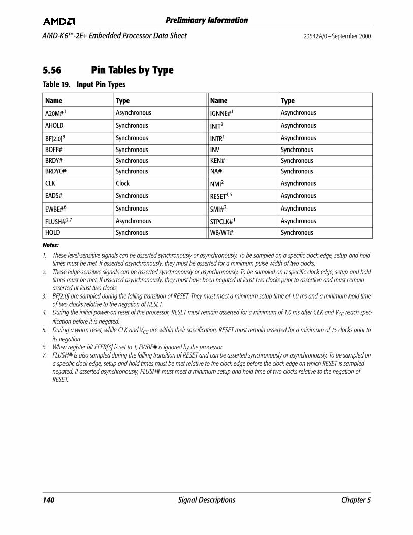
AMD-K6™-2E+ Embedded Processor Data Sheet 23542A/0—September 2000
Preliminary Information
5.56 Pin Tables by TypeTable 19. Input Pin Types
Name Type Name Type
A20M#1
Notes:
1. These level-sensitive signals can be asserted synchronously or asynchronously. To be sampled on a specific clock edge, setup and hold times must be met. If asserted asynchronously, they must be asserted for a minimum pulse width of two clocks.
Asynchronous IGNNE#1 Asynchronous
AHOLD Synchronous INIT2
2. These edge-sensitive signals can be asserted synchronously or asynchronously. To be sampled on a specific clock edge, setup and hold times must be met. If asserted asynchronously, they must have been negated at least two clocks prior to assertion and must remain asserted at least two clocks.
Asynchronous
BF[2:0]3
3. BF[2:0] are sampled during the falling transition of RESET. They must meet a minimum setup time of 1.0 ms and a minimum hold time of two clocks relative to the negation of RESET.
Synchronous INTR1 Asynchronous
BOFF# Synchronous INV Synchronous
BRDY# Synchronous KEN# Synchronous
BRDYC# Synchronous NA# Synchronous
CLK Clock NMI2 Asynchronous
EADS# Synchronous RESET4,5
4. During the initial power-on reset of the processor, RESET must remain asserted for a minimum of 1.0 ms after CLK and VCC reach spec-ification before it is negated.
5. During a warm reset, while CLK and VCC are within their specification, RESET must remain asserted for a minimum of 15 clocks prior to its negation.
Asynchronous
EWBE#6
6. When register bit EFER[3] is set to 1, EWBE# is ignored by the processor.
Synchronous SMI#2 Asynchronous
FLUSH#2,7
7. FLUSH# is also sampled during the falling transition of RESET and can be asserted synchronously or asynchronously. To be sampled on a specific clock edge, setup and hold times must be met relative to the clock edge before the clock edge on which RESET is sampled negated. If asserted asynchronously, FLUSH# must meet a minimum setup and hold time of two clocks relative to the negation of RESET.
Asynchronous STPCLK#1 Asynchronous
HOLD Synchronous WB/WT# Synchronous
140 Signal Descriptions Chapter 5
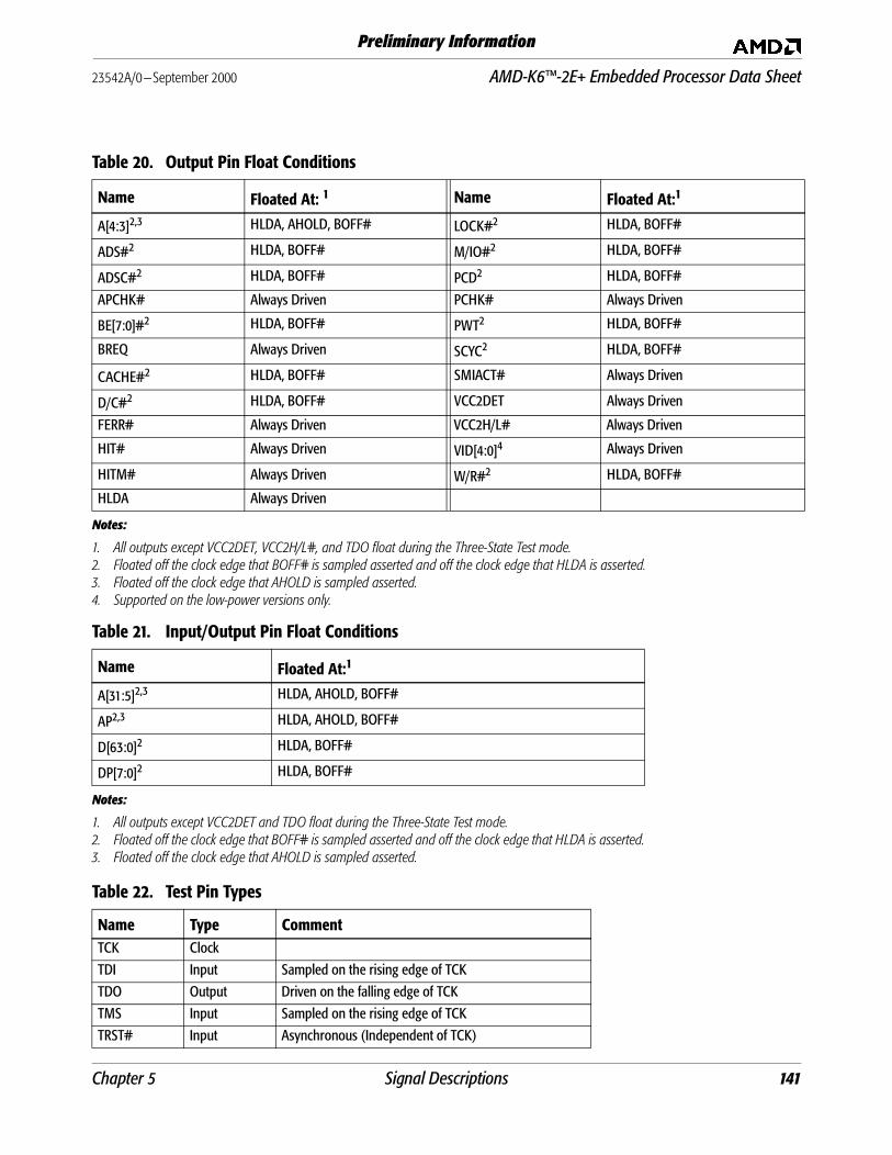
23542A/0—September 2000 AMD-K6™-2E+ Embedded Processor Data Sheet
Preliminary Information
Table 20. Output Pin Float Conditions
Name Floated At: 1
Notes:
1. All outputs except VCC2DET, VCC2H/L#, and TDO float during the Three-State Test mode.
Name Floated At:1
A[4:3]2,3
2. Floated off the clock edge that BOFF# is sampled asserted and off the clock edge that HLDA is asserted.3. Floated off the clock edge that AHOLD is sampled asserted.
HLDA, AHOLD, BOFF# LOCK#2 HLDA, BOFF#
ADS#2 HLDA, BOFF# M/IO#2 HLDA, BOFF#
ADSC#2 HLDA, BOFF# PCD2 HLDA, BOFF#
APCHK# Always Driven PCHK# Always Driven
BE[7:0]#2 HLDA, BOFF# PWT2 HLDA, BOFF#
BREQ Always Driven SCYC2 HLDA, BOFF#
CACHE#2 HLDA, BOFF# SMIACT# Always Driven
D/C#2 HLDA, BOFF# VCC2DET Always Driven
FERR# Always Driven VCC2H/L# Always Driven
HIT# Always Driven VID[4:0]4
4. Supported on the low-power versions only.
Always Driven
HITM# Always Driven W/R#2 HLDA, BOFF#
HLDA Always Driven
Table 21. Input/Output Pin Float Conditions
Name Floated At:1
Notes:
1. All outputs except VCC2DET and TDO float during the Three-State Test mode.
A[31:5]2,3
2. Floated off the clock edge that BOFF# is sampled asserted and off the clock edge that HLDA is asserted.3. Floated off the clock edge that AHOLD is sampled asserted.
HLDA, AHOLD, BOFF#
AP2,3 HLDA, AHOLD, BOFF#
D[63:0]2 HLDA, BOFF#
DP[7:0]2 HLDA, BOFF#
Table 22. Test Pin Types
Name Type CommentTCK Clock
TDI Input Sampled on the rising edge of TCK
TDO Output Driven on the falling edge of TCK
TMS Input Sampled on the rising edge of TCK
TRST# Input Asynchronous (Independent of TCK)
Chapter 5 Signal Descriptions 141

AMD-K6™-2E+ Embedded Processor Data Sheet 23542A/0—September 2000
Preliminary Information
5.57 Bus Cycle DefinitionsTable 23. Bus Cycle Definition
Bus Cycle InitiatedGenerated by the CPU Generated
by System Logic
M/IO# D/C# W/R# CACHE# KEN#Code Read, L1 Instruction Cache and L2 Cache Line Fill 1 0 0 0 0
Code Read, Noncacheable 1 0 0 1 x1
Notes:
1. x means “don’t care”
Code Read, Noncacheable 1 0 0 x 1
Encoding for Special Cycle 0 0 1 1 x
Interrupt Acknowledge 0 0 0 1 x
I/O Read 0 1 0 1 x
I/O Write 0 1 1 1 x
Memory Read, L1 Data Cache and L2 Cache Line Fill 1 1 0 0 0
Memory Read, Noncacheable 1 1 0 1 x
Memory Read, Noncacheable 1 1 0 x 1
Memory Write, L1 Data Cache or L2 Cache Writeback 1 1 1 0 x
Memory Write, Noncacheable 1 1 1 1 x
Table 24. Special Cycles
Special Cycle
A4 BE7#
BE6#
BE5#
BE4#
BE3#
BE2#
BE1#
BE0#
M/I
O#
D/C#
W/R
#
CACH
E#
KEN
#
Stop Grant 1 1 1 1 1 1 0 1 1 0 0 1 1 x1
Notes:
1. x means “don’t care”.
Enhanced Power Management (EPM) Stop Grant2
2. Supported on the low-power versions only.
0 1 0 1 1 1 1 1 1 0 0 1 1 x
Flush Acknowledge (FLUSH# sampled asserted)
0 1 1 1 0 1 1 1 1 0 0 1 1 x
Writeback (WBINVD instruction) 0 1 1 1 1 0 1 1 1 0 0 1 1 x
Halt 0 1 1 1 1 1 0 1 1 0 0 1 1 x
Flush (INVD, WBINVD instruction) 0 1 1 1 1 1 1 0 1 0 0 1 1 x
Shutdown 0 1 1 1 1 1 1 1 0 0 0 1 1 x
142 Signal Descriptions Chapter 5
23542A/0—September 2000 AMD-K6™-2E+ Embedded Processor Data Sheet
Preliminary Information
6 AMD PowerNow!™ Technology
The AMD PowerNow!™ technology is an advanced second-generation power management feature that reduces the overallpower consumed by the processor through control of voltageand frequency. This power saving technology is designed to bedynamic and flexible by enabling instant “on-the-fly” andindependent control of both the processor’s core voltage andfrequency.
AMD PowerNow! technology can be used in conjunction withthe existing power management schemes in an embeddedsystem to provide a better combination of performance andpower savings than previously possible.
6.1 Enhanced Power Management Features
AMD PowerNow! technology-enabled processors include twonew features specifically designed to enhance powermanagement functionality:
■ Dynamic core frequency control
■ Dynamic core voltage control
These enhanced power management features are accessed andcontrolled through an I/O block and two registers:
■ An aligned 16-byte block of I/O address space is defined bythe Enhanced Power Management Register (EPMR).
■ The Enhanced Power Management Register (EPMR) issupported on low-power versions of the processor only.
■ The Processor State Observability Register (PSOR) isdefined differently on the low-power versions of theAMD-K6-2E+ processor to support AMD PowerNow!technology features.
The EPMR and PSOR registers and the I/O block are defined inthis section, followed by a discussion of how to implement anduse the AMD PowerNow! technology features (see “DynamicCore Frequency and Core Voltage Control” on page 150). TheEmbedded AMD-K6™ Processors BIOS Design Guide ApplicationNote, order# 23913, contains additional information.
Chapter 6 AMD PowerNow!™ Technology 143
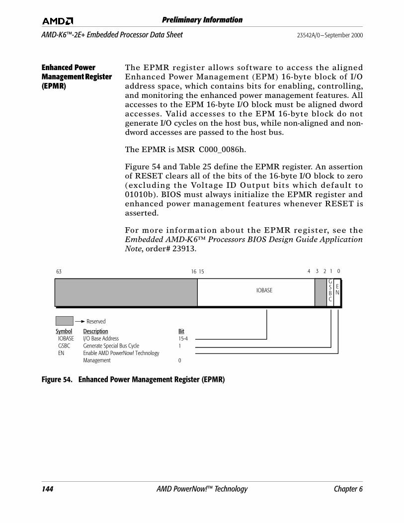
AMD-K6™-2E+ Embedded Processor Data Sheet 23542A/0—September 2000
Preliminary Information
Enhanced Power Management Register (EPMR)
The EPMR register allows software to access the alignedEnhanced Power Management (EPM) 16-byte block of I/Oaddress space, which contains bits for enabling, controlling,and monitoring the enhanced power management features. Allaccesses to the EPM 16-byte I/O block must be aligned dwordaccesses. Valid accesses to the EPM 16-byte block do notgenerate I/O cycles on the host bus, while non-aligned and non-dword accesses are passed to the host bus.
The EPMR is MSR C000_0086h.
Figure 54 and Table 25 define the EPMR register. An assertionof RESET clears all of the bits of the 16-byte I/O block to zero(excluding the Voltage ID Output bits which default to01010b). BIOS must always initialize the EPMR register andenhanced power management features whenever RESET isasserted.
For more information about the EPMR register, see theEmbedded AMD-K6™ Processors BIOS Design Guide ApplicationNote, order# 23913.
Figure 54. Enhanced Power Management Register (EPMR)
Reserved
01663 15 4 3 12
EN
GSBC
IOBASE
Symbol Description BitIOBASE I/O Base Address 15-4GSBC Generate Special Bus Cycle 1EN Enable AMD PowerNow! Technology
Management 0
144 AMD PowerNow!™ Technology Chapter 6
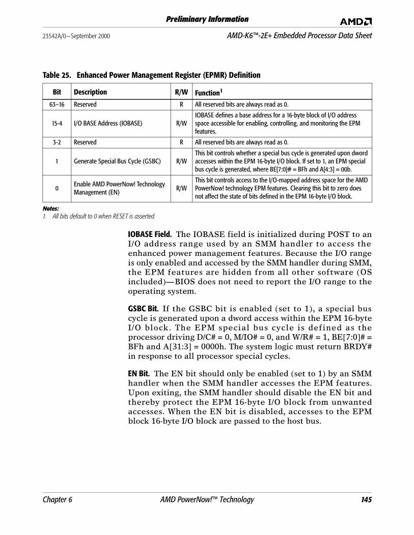
23542A/0—September 2000 AMD-K6™-2E+ Embedded Processor Data Sheet
Preliminary Information
IOBASE Field. The IOBASE field is initialized during POST to anI/O address range used by an SMM handler to access theenhanced power management features. Because the I/O rangeis only enabled and accessed by the SMM handler during SMM,the EPM features are hidden from all other software (OSincluded)—BIOS does not need to report the I/O range to theoperating system.
GSBC Bit. If the GSBC bit is enabled (set to 1), a special buscycle is generated upon a dword access within the EPM 16-byteI/O block. The EPM special bus cycle is defined as theprocessor driving D/C# = 0, M/IO# = 0, and W/R# = 1, BE[7:0]# =BFh and A[31:3] = 0000h. The system logic must return BRDY#in response to all processor special cycles.
EN Bit. The EN bit should only be enabled (set to 1) by an SMMhandler when the SMM handler accesses the EPM features.Upon exiting, the SMM handler should disable the EN bit andthereby protect the EPM 16-byte I/O block from unwantedaccesses. When the EN bit is disabled, accesses to the EPMblock 16-byte I/O block are passed to the host bus.
Table 25. Enhanced Power Management Register (EPMR) Definition
Bit Description R/W Function1
Notes:1. All bits default to 0 when RESET is asserted.
63–16 Reserved R All reserved bits are always read as 0.
15-4 I/O BASE Address (IOBASE) R/WIOBASE defines a base address for a 16-byte block of I/O address space accessible for enabling, controlling, and monitoring the EPM features.
3-2 Reserved R All reserved bits are always read as 0.
1 Generate Special Bus Cycle (GSBC) R/WThis bit controls whether a special bus cycle is generated upon dword accesses within the EPM 16-byte I/O block. If set to 1, an EPM special bus cycle is generated, where BE[7:0]# = BFh and A[4:3] = 00b.
0Enable AMD PowerNow! Technology Management (EN)
R/WThis bit controls access to the I/O-mapped address space for the AMD PowerNow! technology EPM features. Clearing this bit to zero does not affect the state of bits defined in the EPM 16-byte I/O block.
Chapter 6 AMD PowerNow!™ Technology 145
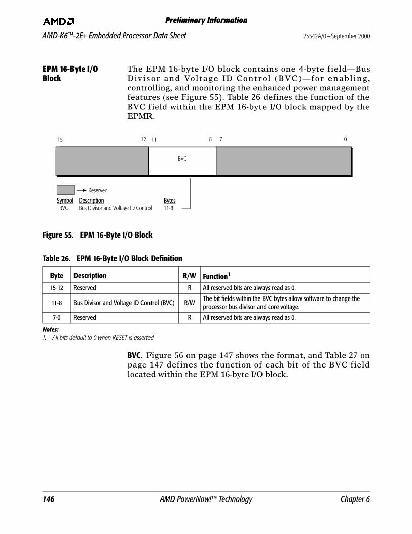
AMD-K6™-2E+ Embedded Processor Data Sheet 23542A/0—September 2000
Preliminary Information
EPM 16-Byte I/O Block
The EPM 16-byte I/O block contains one 4-byte field—BusDivisor and Voltage ID Control (BVC)—for enabling,controlling, and monitoring the enhanced power managementfeatures (see Figure 55). Table 26 defines the function of theBVC field within the EPM 16-byte I/O block mapped by theEPMR.
Figure 55. EPM 16-Byte I/O Block
BVC. Figure 56 on page 147 shows the format, and Table 27 onpage 147 defines the function of each bit of the BVC fieldlocated within the EPM 16-byte I/O block.
Table 26. EPM 16-Byte I/O Block Definition
Byte Description R/W Function1
Notes:1. All bits default to 0 when RESET is asserted.
15-12 Reserved R All reserved bits are always read as 0.
11-8 Bus Divisor and Voltage ID Control (BVC) R/WThe bit fields within the BVC bytes allow software to change the processor bus divisor and core voltage.
7-0 Reserved R All reserved bits are always read as 0.
Reserved
01215 11 8 7
BVC
Symbol Description BytesBVC Bus Divisor and Voltage ID Control 11-8
146 AMD PowerNow!™ Technology Chapter 6
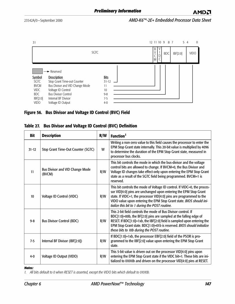
23542A/0—September 2000 AMD-K6™-2E+ Embedded Processor Data Sheet
Preliminary Information
Figure 56. Bus Divisor and Voltage ID Control (BVC) Field
Table 27. Bus Divisor and Voltage ID Control (BVC) Definition
Bit Description R/W Function1
Notes:1. All bits default to 0 when RESET is asserted, except the VIDO bits which default to 01010b.
31-12 Stop Grant Time-Out Counter (SGTC) W
Writing a non-zero value to this field causes the processor to enter the EPM Stop Grant state internally. This 20-bit value is multiplied by 4096 to determine the duration of the EPM Stop Grant state, measured in processor bus clocks.
11Bus Divisor and VID Change Mode (BVCM)
R/W
This bit controls the mode in which the bus-divisor and the voltage control bits are allowed to change. If BVCM=0, the Bus Divisor and Voltage ID changes take effect only upon entering the EPM Stop Grant state as a result of the SGTC field being programmed. BVCM=1 is reserved.
10 Voltage ID Control (VIDC) R/W
This bit controls the mode of Voltage ID control. If VIDC=0, the proces-sor VID[4:0] pins are unchanged upon entering the EPM Stop Grant state. If VIDC=1, the processor VID[4:0] pins are programmed to the VIDO value upon entering the EPM Stop Grant state. BIOS should ini-tialize this bit to 1 during the POST routine.
9-8 Bus Divisor Control (BDC) R/W
This 2-bit field controls the mode of Bus Divisor control. If BDC[1:0]=00b, the BF[2:0] pins are sampled at the falling edge of RESET. If BDC[1:0]=1xb, the IBF[2:0] field is sampled upon entering the EPM Stop Grant state. BDC[1:0]=01b is reserved. BIOS should initialize these bits to 10b during the POST routine.
7-5 Internal BF Divisor (IBF[2:0]) R/WIf BDC[1:0]=1xb, the processor EBF[2:0] field of the PSOR is pro-grammed to the IBF[2:0] value upon entering the EPM Stop Grant state.
4-0 Voltage ID Output (VIDO) R/WThis 5-bit value is driven out on the processor VID[4:0] pins upon entering the EPM Stop Grant state if the VIDC bit=1. These bits are ini-tialized to 01010b and driven on the processor VID[4:0] pins at RESET.
Reserved
01231 9 8 7 5
Symbol Description BitsSGTC Stop Grant Time-out Counter 31-12BVCM Bus Divisor and VID Change Mode 11VIDC Voltage ID Control 10BDC Bus Divisor Control 9-8IBF[2:0] Internal BF Divisor 7-5VIDO Voltage ID Output 4-0
VIDC
IBF[2:0]
11 10
BVCM
BDC VIDO
4
SGTC
Chapter 6 AMD PowerNow!™ Technology 147
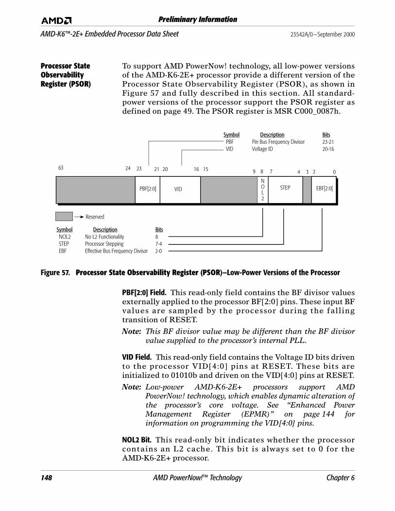
AMD-K6™-2E+ Embedded Processor Data Sheet 23542A/0—September 2000
Preliminary Information
Processor State Observability Register (PSOR)
To support AMD PowerNow! technology, all low-power versionsof the AMD-K6-2E+ processor provide a different version of theProcessor State Observability Register (PSOR), as shown inFigure 57 and fully described in this section. All standard-power versions of the processor support the PSOR register asdefined on page 49. The PSOR register is MSR C000_0087h..
Figure 57. Processor State Observability Register (PSOR)—Low-Power Versions of the Processor
PBF[2:0] Field. This read-only field contains the BF divisor valuesexternally applied to the processor BF[2:0] pins. These input BFvalues are sampled by the processor during the fallingtransition of RESET.
Note: This BF divisor value may be different than the BF divisorvalue supplied to the processor’s internal PLL.
VID Field. This read-only field contains the Voltage ID bits drivento the processor VID[4:0] pins at RESET. These bits areinitialized to 01010b and driven on the VID[4:0] pins at RESET.
Note: Low-power AMD-K6-2E+ processors support AMDPowerNow! technology, which enables dynamic alteration ofthe processor’s core voltage. See “Enhanced PowerManagement Register (EPMR)” on page 144 forinformation on programming the VID[4:0] pins.
NOL2 Bit. This read-only bit indicates whether the processorcontains an L2 cache. This bit is always set to 0 for theAMD-K6-2E+ processor.
2 063
EBF[2:0]
Reserved
Symbol Description BitsNOL2 No L2 Functionality 8STEP Processor Stepping 7-4EBF Effective Bus Frequency Divisor 2-0
34
STEP
789
NOL2
VIDPBF[2:0]
162023 21 1524
Symbol Description BitsPBF Pin Bus Frequency Divisor 23-21VID Voltage ID 20-16
148 AMD PowerNow!™ Technology Chapter 6
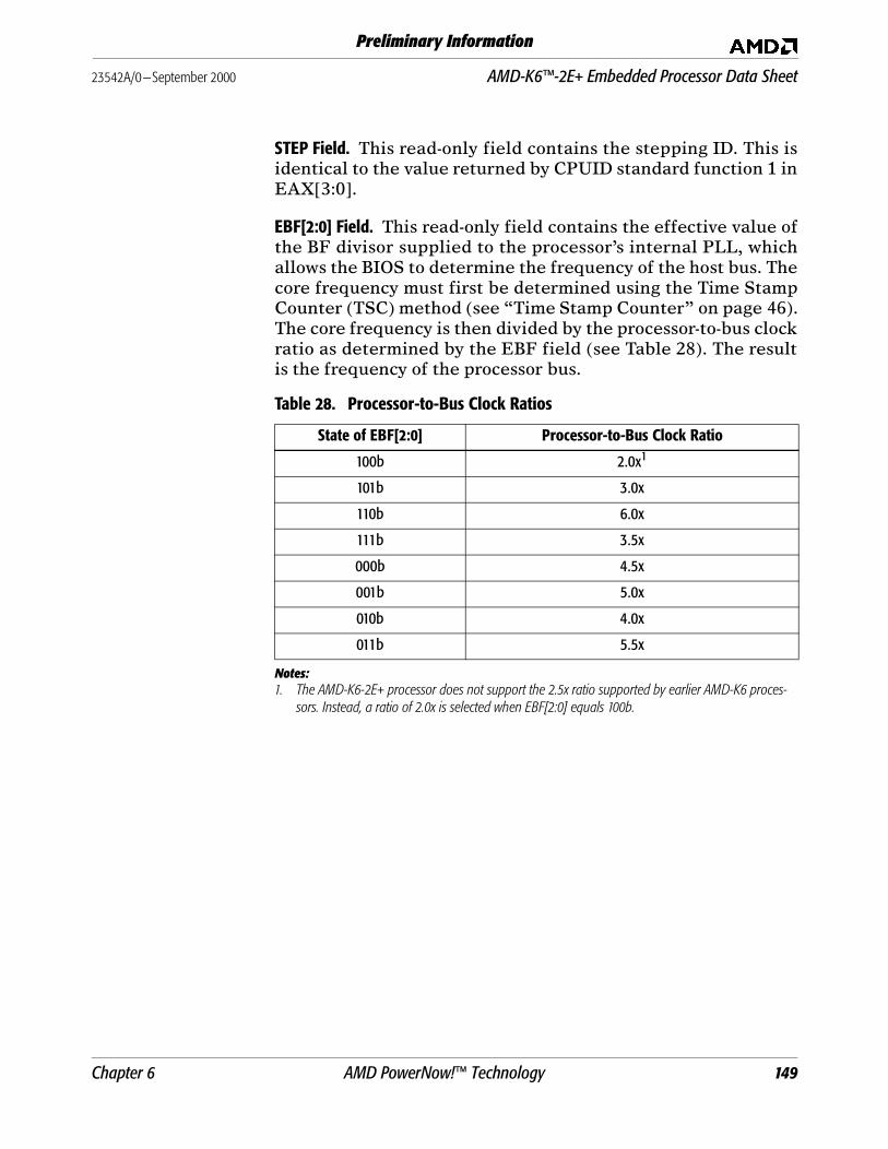
23542A/0—September 2000 AMD-K6™-2E+ Embedded Processor Data Sheet
Preliminary Information
STEP Field. This read-only field contains the stepping ID. This isidentical to the value returned by CPUID standard function 1 inEAX[3:0].
EBF[2:0] Field. This read-only field contains the effective value ofthe BF divisor supplied to the processor’s internal PLL, whichallows the BIOS to determine the frequency of the host bus. Thecore frequency must first be determined using the Time StampCounter (TSC) method (see “Time Stamp Counter” on page 46).The core frequency is then divided by the processor-to-bus clockratio as determined by the EBF field (see Table 28). The resultis the frequency of the processor bus.
Table 28. Processor-to-Bus Clock Ratios
State of EBF[2:0] Processor-to-Bus Clock Ratio
100b 2.0x1
Notes:1. The AMD-K6-2E+ processor does not support the 2.5x ratio supported by earlier AMD-K6 proces-
sors. Instead, a ratio of 2.0x is selected when EBF[2:0] equals 100b.
101b 3.0x
110b 6.0x
111b 3.5x
000b 4.5x
001b 5.0x
010b 4.0x
011b 5.5x
Chapter 6 AMD PowerNow!™ Technology 149
AMD-K6™-2E+ Embedded Processor Data Sheet 23542A/0—September 2000
Preliminary Information
6.2 Dynamic Core Frequency and Core Voltage Control
AMD PowerNow! technology-enabled processors support theability to change the bus frequency divisor and core voltagetransparently to the user during run-time. These features areimplemented in conjunction with a new clock control state—the EPM Stop Grant state.
For AMD PowerNow! technology state transitions, the EPMRregister is accessed using an SMM handler.
■ The SMM handler initiates core voltage and frequencytransitions by writing a non-zero value to the Stop GrantTime-Out Counter (SGTC) field.
■ This action automatically places the processor into the EPMStop Grant State and transitions the CPU core voltage andfrequency to the values specified in the Voltage ID Output(VIDO) and Internal BF Divisor (IBF) fields of the BVC field.
■ Once the timer of the SGTC has expired, the EPM StopGrant State is exited and the AMD PowerNow! technologystate transition is completed.
See “Clock Control” on page 275 for more information aboutthe EPM Stop Grant State.
Effective Bus Frequency Divisor (EBF[2:0])
The processor core frequency is controlled by the Effective BusFrequency Divisor—EBF[2:0]—which dictates the processor-to-bus clock ratio supplied to the processor’s internal PLL. Thisprocessor-to-bus clock ratio is multiplied by the external busfrequency to set the frequency of operation for the processorcore.
■ At the fall of RESET, the EBF[2:0] value is determined bythe state of the processor BF[2:0] input pins.
■ Afterwards, the EBF[2:0] value can be dynamicallycontrolled through AMD PowerNow! technology statetransitions.
Table 28 on page 149 lists valid EBF[2:0] states and equivalentprocessor-to-bus clock ratios.
150 AMD PowerNow!™ Technology Chapter 6
23542A/0—September 2000 AMD-K6™-2E+ Embedded Processor Data Sheet
Preliminary Information
Dynamic Core Frequency Control
For AMD PowerNow! technology core frequency transitions,the BVC field of the EPM 16-byte I/O block is accessed throughan SMM handler.
■ To change the processor core frequency, the SMM handlerinitiates core voltage and frequency transitions by writing anon-zero value to the SGTC field.
■ This action automatically places the processor into the EPMStop Grant state and transitions the CPU core voltage andfrequency to the values specified in the VIDO and IBF fieldsof the BVC field.
Note: System-initiated inquire (snoop) cycles are not supportedand must be prevented during the EPM Stop Grant state.
Voltage Identification (VID) Outputs
AMD PowerNow! technology-enabled processors featureVoltage ID (VID) outputs to support dynamic control of thecore voltage.
■ These outputs serve as inputs to a DC/DC regulator thatsupplies the processor core voltage.
■ Based on its VID[4:0] inputs, the regulator outputs acorresponding voltage.
■ For those regulators that do not support VID inputs, theprocessor VID[4:0] outputs must be used to manipulate theregulator’s feedback voltage to vary the regulator outputvoltage.
Chapter 6 AMD PowerNow!™ Technology 151
AMD-K6™-2E+ Embedded Processor Data Sheet 23542A/0—September 2000
Preliminary Information
152 AMD PowerNow!™ Technology Chapter 6
23542A/0—September 2000 AMD-K6™-2E+ Embedded Processor Data Sheet
Preliminary Information
7 Bus Cycles
The following sections describe and illustrate the timing andrelationship of bus signals during various types of bus cycles. Arepresentative set of bus cycles is illustrated.
7.1 Timing Diagrams
The timing diagrams illustrate the signals on the external localbus as a function of time, as measured by the bus clock (CLK).
Bus Clock (CLK) Throughout this chapter, the term clock refers to a singlebus-clock cycle. A clock extends from one rising CLK edge tothe next rising CLK edge. The processor samples and drivesmost signals relative to the rising edge of CLK. The exceptionsto this rule include the following:
■ BF[2:0]—Sampled on the falling edge of RESET
■ FLUSH#—Sampled on the falling edge of RESET, alsosampled on the rising edge of CLK
■ All inputs and outputs are sampled relative to TCK inBoundary-Scan Test Mode. Inputs are sampled on the risingedge of TCK, outputs are driven off of the falling edge ofTCK.
Waveform Definitions
For each signal in the timing diagrams, the High levelrepresents 1, the Low level represents 0, and the Middle levelrepresents the floating (high-impedance) state.
When both the High and Low levels are shown, the meaningdepends on the signal:
■ A single signal indicates ‘don’t care’.
■ In the case of bus activity, if both High and Low levels areshown, it indicates that the processor, alternate master, orsystem logic is driving a value, but this value may or may notbe valid. (For example, the value on the address bus is validonly during the assertion of ADS#, but addresses are alsodriven on the bus at other times.)
Figure 58 on page 154 defines the different waveformrepresentations.
Chapter 7 Bus Cycles 153
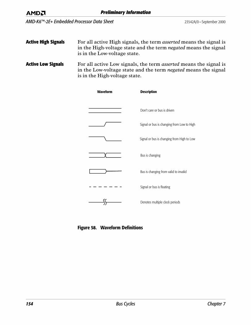
AMD-K6™-2E+ Embedded Processor Data Sheet 23542A/0—September 2000
Preliminary Information
Active High Signals For all active High signals, the term asserted means the signal isin the High-voltage state and the term negated means the signalis in the Low-voltage state.
Active Low Signals For all active Low signals, the term asserted means the signal isin the Low-voltage state and the term negated means the signalis in the High-voltage state.
Figure 58. Waveform Definitions
Waveform
Don’t care or bus is driven
Description
Signal or bus is changing from Low to High
Signal or bus is changing from High to Low
Bus is changing
Bus is changing from valid to invalid
Signal or bus is floating
Denotes multiple clock periods
154 Bus Cycles Chapter 7
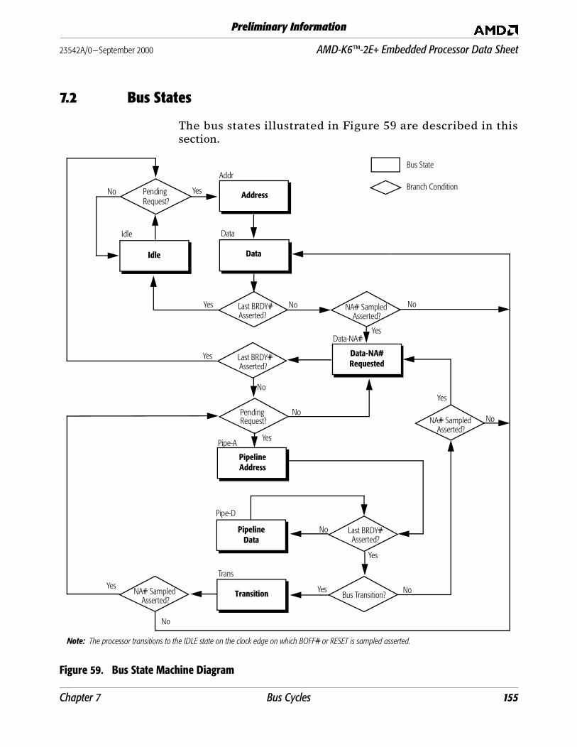
23542A/0—September 2000 AMD-K6™-2E+ Embedded Processor Data Sheet
Preliminary Information
7.2 Bus States
The bus states illustrated in Figure 59 are described in thissection.
Figure 59. Bus State Machine Diagram
Last BRDY#
Last BRDY#
Bus Transition?
No
Yes
Yes
Yes
Yes
No
No
No
No
PendingRequest?
NA# SampledAsserted?
NA# SampledAsserted?
Asserted?
Asserted?
Addr
Data
Pipe-A
Pipe-D
Idle
Trans
Bus State
Branch Condition
Idle Data
PipelineAddress
Transition
Address
PipelineData
Note: The processor transitions to the IDLE state on the clock edge on which BOFF# or RESET is sampled asserted.
Data-NA#Requested
Data-NA#
Last BRDY#Yes
No
Asserted?
PendingRequest?
No
Yes
No
Yes
Yes
NA# SampledAsserted?
Yes
No
Chapter 7 Bus Cycles 155
AMD-K6™-2E+ Embedded Processor Data Sheet 23542A/0—September 2000
Preliminary Information
Idle The processor does not drive the system bus in the Idle stateand remains in this state until a new bus cycle is requested. Theprocessor enters this state off the clock edge on which the lastBRDY# of a cycle is sampled asserted during the followingconditions:
■ The processor is in the Data state
■ The processor is in the Data-NA# Requested state and nointernal pending cycle is requested
In addition, the processor is forced into this state when thesystem logic asserts RESET or BOFF#. The transition to thisstate occurs on the clock edge on which RESET or BOFF# issampled asserted.
Address In this state, the processor drives ADS# to indicate thebeginning of a new bus cycle by validating the address andcontrol signals. The processor remains in this state for one clockand unconditionally enters the Data state on the next clockedge.
Data In the Data state, the processor drives the data bus during awrite cycle or expects data to be returned during a read cycle.The processor remains in this state until either NA# or the lastBRDY# is sampled asserted. If the last BRDY# is sampledasserted or both the last BRDY# and NA# are sampled assertedon the same clock edge, the processor enters the Idle state. IfNA# is sampled asserted first, the processor enters theData-NA# Requested state.
Data-NA# Requested If the processor samples NA# asserted while in the Data stateand the current bus cycle is not completed (the last BRDY# isnot sampled asserted), it enters the Data-NA# Requested state.The processor remains in this state until either the last BRDY#is sampled asserted or an internal pending cycle is requested. Ifthe last BRDY# is sampled asserted before the processor drivesa new bus cycle, the processor enters the Idle state (no internalpending cycle is requested) or the Address state (processor hasa internal pending cycle).
Pipeline Address In this state, the processor drives ADS#, indicating thebeginning of a new bus cycle and validating the address andcontrol signals. In this state, the processor is still waiting for thecurrent bus cycle to be completed (until the last BRDY# is
156 Bus Cycles Chapter 7

23542A/0—September 2000 AMD-K6™-2E+ Embedded Processor Data Sheet
Preliminary Information
sampled asserted). If the last BRDY# is not sampled asserted,the processor enters the Pipeline Data state.
If the processor samples the last BRDY# asserted in this state, itdetermines if a bus transition is required between the currentbus cycle and the pipelined bus cycle. A bus transition isrequired when the data bus direction changes between buscycles, such as a memory write cycle followed by a memory readcycle. If a bus transition is required, the processor enters theTransition state for one clock to prevent data bus contention. Ifa bus transition is not required, the processor enters the Datastate.
The processor does not transition to the Data-NA# Requestedstate from the Pipeline Address state because the processordoes not begin sampling NA# until it has exited the PipelineAddress state.
Pipeline Data Two bus cycles are executing concurrently in this state. Theprocessor cannot issue any additional bus cycles until thecurrent bus cycle is completed. The processor drives the databus during write cycles or expects data to be returned duringread cycles for the current bus cycle until the last BRDY# of thecurrent bus cycle is sampled asserted.
If the processor samples the last BRDY# asserted in this state, itdetermines if a bus transition is required between the currentbus cycle and the pipelined bus cycle. If the bus transition isrequired, the processor enters the Transition state for one clockto prevent data bus contention. If a bus transition is notrequired, the processor enters the Data state (NA# was notsampled asserted) or the Data-NA# Requested state (NA# wassampled asserted).
Transition The processor enters this state for one clock during data bustransitions and enters the Data state on the next clock edge ifNA# is not sampled asserted. The sole purpose of this state is toavoid bus contention caused by bus transitions during pipelineoperation.
Chapter 7 Bus Cycles 157

AMD-K6™-2E+ Embedded Processor Data Sheet 23542A/0—September 2000
Preliminary Information
7.3 Memory Reads and Writes
The AMD-K6-2E+ processor performs single or burst-memorybus cycles.
■ The single-transfer memory bus cycle transfers 1, 2, 4, or 8bytes and requires a minimum of two clocks.
■ Misaligned instructions or operands result in a split cycle,which requires multiple transactions on the bus.
■ A burst cycle consists of four back-to-back 8-byte (64-bit)transfers on the data bus.
Single-Transfer Memory Read and Write
Figure 60 on page 159 shows a single-transfer read frommemory, followed by two single-transfer writes to memory. Forthe memory read cycle, the processor asserts ADS# for oneclock to validate the bus cycle and also drives A[31:3], BE[7:0]#,D/C#, W/R#, and M/IO# to the bus. The processor then waits forthe system logic to return the data on D[63:0] (with DP[7:0] forparity checking) and assert BRDY#. The processor samplesBRDY# on every clock edge starting with the clock edge afterthe clock edge that negates ADS#. See “BRDY# (Burst Ready)”on page 103.
During the read cycle, the processor drives PCD, PWT, andCACHE# to indicate its caching and cache-coherency intent forthe access. The system logic returns KEN# and WB/WT# toeither confirm or change this intent. If the processor assertsPCD and negates CACHE#, the accesses are noncacheable, eventhough the system logic asserts KEN# during the BRDY# toindicate its support for cacheability. The processor (whichdrives CACHE#) and the system logic (which drives KEN#) mustagree in order for an access to be cacheable.
The processor can drive another cycle (in this example, a writecycle) by asserting ADS# off the next clock edge after BRDY# issampled asserted. Therefore, an idle clock is guaranteedbetween any two bus cycles. The processor drives D[63:0] withvalid data one clock edge after the clock edge on which ADS# isasserted. To minimize processor idle times, the system logicstores the address and data in write buffers, returns BRDY#,and performs the store to memory later. If the processorsamples EWBE# negated during a write cycle, it suspendscertain activities until EWBE# is sampled asserted. See“EWBE# (External Write Buffer Empty)” on page 110. In
158 Bus Cycles Chapter 7
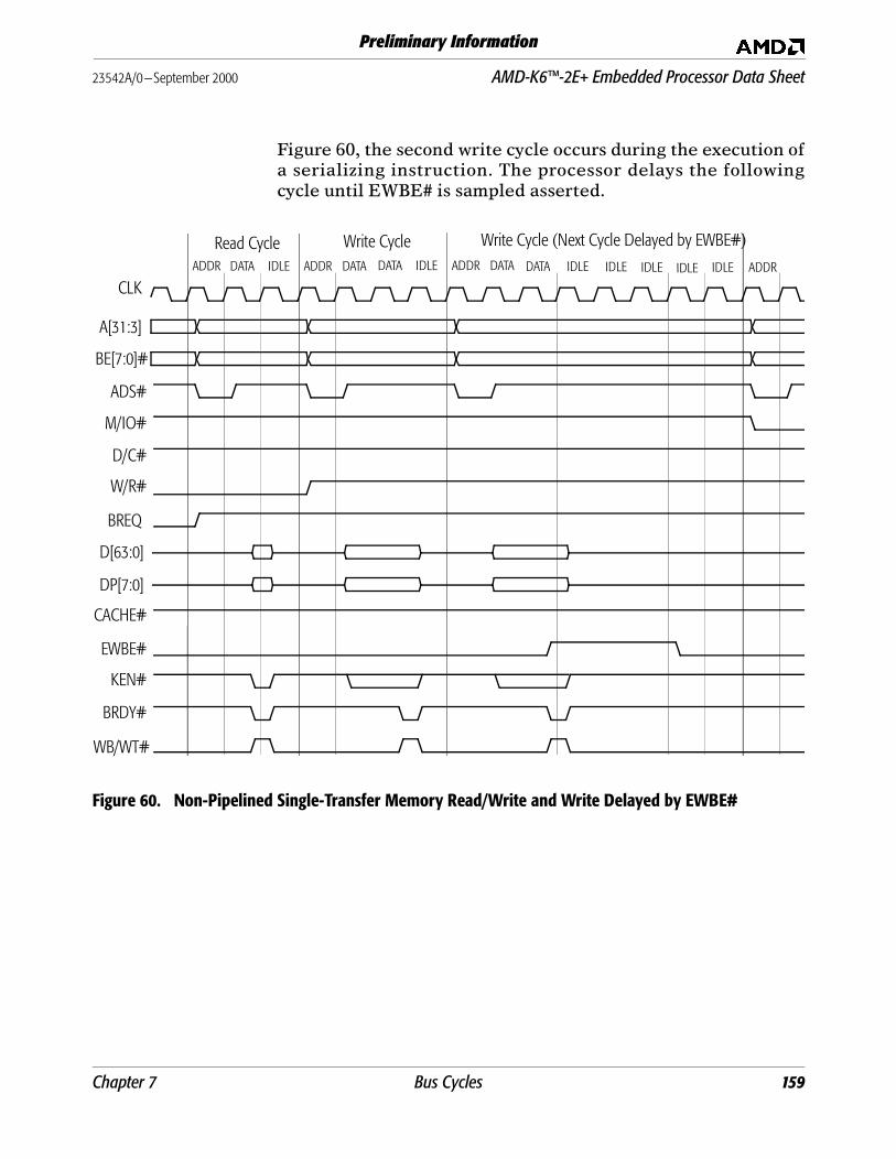
23542A/0—September 2000 AMD-K6™-2E+ Embedded Processor Data Sheet
Preliminary Information
Figure 60, the second write cycle occurs during the execution ofa serializing instruction. The processor delays the followingcycle until EWBE# is sampled asserted.
Figure 60. Non-Pipelined Single-Transfer Memory Read/Write and Write Delayed by EWBE#
Read Cycle Write Cycle (Next Cycle Delayed by EWBE#)Write Cycle
CLK
A[31:3]
BE[7:0]#
ADS#
M/IO#
D/C#
W/R#
BREQ
D[63:0]
DP[7:0]
CACHE#
EWBE#
KEN#
BRDY#
WB/WT#
ADDR DATA IDLE ADDR ADDRDATA IDLEDATA DATA DATA IDLE IDLE IDLE IDLE IDLE ADDR
Chapter 7 Bus Cycles 159

AMD-K6™-2E+ Embedded Processor Data Sheet 23542A/0—September 2000
Preliminary Information
Misaligned Single-Transfer Memory Read and Write
Figure 61 on page 161 shows a misaligned (split) memory readfollowed by a misaligned memory write. Any cycle that is notaligned as defined in “SCYC (Split Cycle)” on page 129 isconsidered misaligned. When the processor encounters amisaligned access, it determines the appropriate pair of buscycles—each with its own ADS# and BRDY#— required tocomplete the access.
The AMD-K6-2E+ processor performs misaligned memory readsand memory writes using least-significant bytes (LSBs) firstfollowed by most-significant bytes (MSBs). Table 29 shows theorder. In the first memory read cycle in Figure 61, the processorreads the least-significant bytes. Immediately after theprocessor samples BRDY# asserted, it drives the second buscycle to read the most-significant bytes to complete themisaligned transfer.
Similarly, the misaligned memory write cycle in Figure 61transfers the LSBs to the memory bus first. In the next cycle,after the processor samples BRDY# asserted, the MSBs arewritten to the memory bus.
Table 29. Bus-Cycle Order During Misaligned Memory Transfers
Type of Access First Cycle Second CycleMemory Read LSBs MSBs
Memory Write LSBs MSBs
160 Bus Cycles Chapter 7

23542A/0—September 2000 AMD-K6™-2E+ Embedded Processor Data Sheet
Preliminary Information
Figure 61. Misaligned Single-Transfer Memory Read and Write
LSB MSB LSB MSB
Memory Read (Misaligned) Memory Write (Misaligned)
CLK
A[31:3]
BE[7:0]#
ADS#
M/IO#
D/C#
W/R#
D[63:0]
BRDY#
ADDR DATA DATA IDLE ADDR DATA DATA IDLE ADDR DATA DATA IDLEDATA ADDR DATA DATA IDLEDATA
Chapter 7 Bus Cycles 161
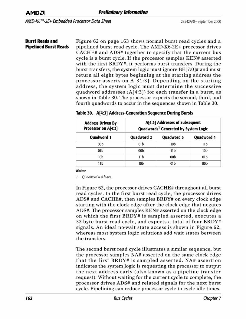
AMD-K6™-2E+ Embedded Processor Data Sheet 23542A/0—September 2000
Preliminary Information
Burst Reads and Pipelined Burst Reads
Figure 62 on page 163 shows normal burst read cycles and apipelined burst read cycle. The AMD-K6-2E+ processor drivesCACHE# and ADS# together to specify that the current buscycle is a burst cycle. If the processor samples KEN# assertedwith the first BRDY#, it performs burst transfers. During theburst transfers, the system logic must ignore BE[7:0]# and mustreturn all eight bytes beginning at the starting address theprocessor asserts on A[31:3]. Depending on the startingaddress, the system logic must determine the successivequadword addresses (A[4:3]) for each transfer in a burst, asshown in Table 30. The processor expects the second, third, andfourth quadwords to occur in the sequences shown in Table 30.
In Figure 62, the processor drives CACHE# throughout all burstread cycles. In the first burst read cycle, the processor drivesADS# and CACHE#, then samples BRDY# on every clock edgestarting with the clock edge after the clock edge that negatesADS#. The processor samples KEN# asserted on the clock edgeon which the first BRDY# is sampled asserted, executes a32-byte burst read cycle, and expects a total of four BRDY#signals. An ideal no-wait state access is shown in Figure 62,whereas most system logic solutions add wait states betweenthe transfers.
The second burst read cycle illustrates a similar sequence, butthe processor samples NA# asserted on the same clock edgethat the first BRDY# is sampled asserted. NA# assertionindicates the system logic is requesting the processor to outputthe next address early (also known as a pipeline transferrequest). Without waiting for the current cycle to complete, theprocessor drives ADS# and related signals for the next burstcycle. Pipelining can reduce processor cycle-to-cycle idle times.
Table 30. A[4:3] Address-Generation Sequence During Bursts
Address Driven By Processor on A[4:3]
A[4:3] Addresses of SubsequentQuadwords1 Generated by System Logic
Notes:
1. Quadword = 8 bytes.
Quadword 1 Quadword 2 Quadword 3 Quadword 400b 01b 10b 11b
01b 00b 11b 10b
10b 11b 00b 01b
11b 10b 01b 00b
162 Bus Cycles Chapter 7

23542A/0—September 2000 AMD-K6™-2E+ Embedded Processor Data Sheet
Preliminary Information
Figure 62. Burst Reads and Pipelined Burst Reads
-NA -ADDR
DATA1 DATA2 DATA3
Burst Read Pipelined Burst Read
ADDR1 ADDR2 ADDR3
Burst Read
CLK
A[31:3]
BE[7:0]#
ADS#
M/IO#
D/C#
W/R#
NA#
D[63:0]
CACHE#
KEN#
BRDY#
ADDR DATA IDLEDATADATADATA ADDR DATA DATA DATA PIPE DATA DATA DATA DATA IDLE
Chapter 7 Bus Cycles 163
AMD-K6™-2E+ Embedded Processor Data Sheet 23542A/0—September 2000
Preliminary Information
Burst Writeback Figure 63 on page 165 shows a burst read followed by awriteback transaction. The AMD-K6-2E+ processor initiateswritebacks under the following conditions:
■ Replacement—If a cache-line fill is initiated for a cache linecurrently filled with valid entries, the processor selects aline for replacement based on a least-recently-used (LRU)algorithm for the L1 instruction cache and the L2 cache, anda least-recently-allocated (LRA) algorithm for the L1 datacache. Before a replacement is made to a L1 data cache or L2cache line that is in the modified state, the modified line isscheduled to be written back to memory.
■ Internal Snoop—The processor snoops its L1 instructioncache during read or write misses to its L1 data cache, and itsnoops its L1 data cache during read misses to its L1instruction cache. This snooping is performed to determinewhether the same address is stored in both caches, asituation that is taken to imply the occurrence ofself-modifying code. If an internal snoop hits a L1 data cacheline in the modified state, the line is written back to memorybefore being invalidated.
■ WBINVD Instruction—When the processor executes aWBINVD instruction, it writes back all modified lines in theL1 data cache and L2 cache, and then invalidates all lines inall caches.
■ Cache Flush—When the processor samples FLUSH#asserted, it executes a flush acknowledge special cycle andwrites back all modified lines in the L1 data cache and L2cache, and then invalidates all lines in all caches.
The processor drives writeback cycles during inquire or cacheflush cycles. The writeback shown in Figure 63 is caused by acache-line replacement. The processor completes the burst readcycle that fills the cache line. Immediately following the burstread cycle is the burst writeback cycle that represents themodified line to be written back to memory. D[63:0] are drivenone clock edge after the clock edge on which ADS# is assertedand are subsequently changed off the clock edge on which eachof the four BRDY# signals of the burst cycle are sampledasserted.
164 Bus Cycles Chapter 7

23542A/0—September 2000 AMD-K6™-2E+ Embedded Processor Data Sheet
Preliminary Information
Figure 63. Burst Writeback due to Cache-Line Replacement
Burst Read Burst Writeback from L1 Cache
CLK
A[31:3]
BE[7:0]#
ADS#
CACHE#
M/IO#
D/C#
W/R#
D[63:0]
KEN#
BRDY#
WB/WT#
ADDR DATA IDLEDATADATA DATA ADDR DATA IDLEDATADATA DATA
Chapter 7 Bus Cycles 165
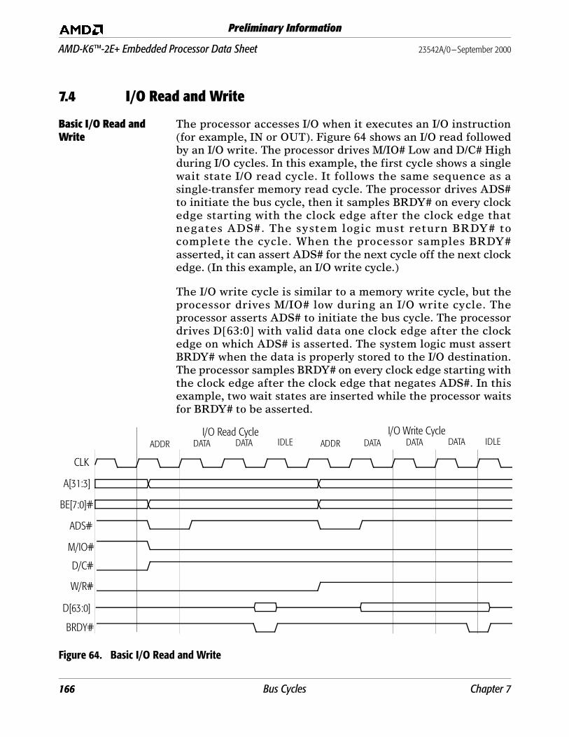
AMD-K6™-2E+ Embedded Processor Data Sheet 23542A/0—September 2000
Preliminary Information
7.4 I/O Read and Write
Basic I/O Read and Write
The processor accesses I/O when it executes an I/O instruction(for example, IN or OUT). Figure 64 shows an I/O read followedby an I/O write. The processor drives M/IO# Low and D/C# Highduring I/O cycles. In this example, the first cycle shows a singlewait state I/O read cycle. It follows the same sequence as asingle-transfer memory read cycle. The processor drives ADS#to initiate the bus cycle, then it samples BRDY# on every clockedge starting with the clock edge after the clock edge thatnegates ADS#. The system logic must return BRDY# tocomplete the cycle. When the processor samples BRDY#asserted, it can assert ADS# for the next cycle off the next clockedge. (In this example, an I/O write cycle.)
The I/O write cycle is similar to a memory write cycle, but theprocessor drives M/IO# low during an I/O write cycle. Theprocessor asserts ADS# to initiate the bus cycle. The processordrives D[63:0] with valid data one clock edge after the clockedge on which ADS# is asserted. The system logic must assertBRDY# when the data is properly stored to the I/O destination.The processor samples BRDY# on every clock edge starting withthe clock edge after the clock edge that negates ADS#. In thisexample, two wait states are inserted while the processor waitsfor BRDY# to be asserted.
Figure 64. Basic I/O Read and Write
I/O Read Cycle I/O Write Cycle
CLK
A[31:3]
BE[7:0]#
ADS#
M/IO#
D/C#
W/R#
D[63:0]
BRDY#
ADDR DATA DATA IDLE ADDR DATA DATA DATA IDLE
166 Bus Cycles Chapter 7

23542A/0—September 2000 AMD-K6™-2E+ Embedded Processor Data Sheet
Preliminary Information
Misaligned I/O Read and Write
Table 31 shows the misaligned I/O read and write cycle orderexecuted by the AMD-K6-2E+ processor. In Figure 65, theleast-significant bytes (LSBs) are transferred first. Immediatelyafter the processor samples BRDY# asserted, it drives thesecond bus cycle to transfer the most-significant bytes (MSBs)to complete the misaligned bus cycle.
Figure 65. Misaligned I/O Transfer
Table 31. Bus-Cycle Order During Misaligned I/O Transfers
Type of Access First Cycle Second CycleI/O Read LSBs MSBs
I/O Write LSBs MSBs
LSB MSB LSB MSB
Misaligned I/O Read Misaligned I/O Write
CLK
A[31:3]
BE[7:0]#
ADS#
M/IO#
D/C#
W/R#
D[63:0]
BRDY#
ADDR DATA DATA IDLE ADDR DATA DATA IDLE ADDR DATA DATADATA IDLE ADDR DATA DATADATA IDLE
SCYC
Chapter 7 Bus Cycles 167
AMD-K6™-2E+ Embedded Processor Data Sheet 23542A/0—September 2000
Preliminary Information
7.5 Inquire and Bus Arbitration Cycles
The AMD-K6-2E+ processor provides built-in level-one (L1)data and instruction caches, and a unified level-two (L2) cache.Each L1 cache is 32 Kbytes and two-way set-associative. The L2cache is 128 Kbytes and four-way set-associative. The systemlogic or other bus master devices can initiate an inquire cycle tomaintain cache/memory coherency. In response to the inquirecycle, the processor compares the inquire address with its cachetag addresses in all caches, and, if necessary, updates the MESIstate of the cache line and performs writebacks to memory.
An inquire cycle can be initiated by asserting AHOLD, BOFF#,or HOLD. AHOLD is exclusively used to support inquire cycles.During AHOLD-initiated inquire cycles, the processor onlyfloats the address bus. BOFF# provides the fastest access to thebus because it aborts any processor cycle that is in-progress,whereas AHOLD and HOLD both permit an in-progress buscycle to complete. During HOLD-initiated and BOFF#-initiatedinquire cycles, the processor floats all of its bus-driving signals.
The AMD-K6-2E+ processor does not support system-initiatedinquire cycles during the Enhanced Power Management (EPM)Stop Grant State. For more information on the EPM Stop GrantState, see “Clock Control” on page 275.
Hold and Hold Acknowledge Cycle
The system logic or another bus device can assert HOLD toinitiate an inquire cycle or to gain full control of the bus. Whenthe AMD-K6-2E+ processor samples HOLD asserted, itcompletes any in-progress bus cycle and asserts HLDA toacknowledge release of the bus. The processor floats thefollowing signals off the same clock edge on which HLDA isasserted:
■ A[31:3] ■ DP[7:0]■ ADS# ■ LOCK#■ AP# ■ M/IO#■ BE[7:0]# ■ PCD■ CACHE# ■ PWT■ D[63:0] ■ SCYC■ D/C# ■ W/R#
168 Bus Cycles Chapter 7
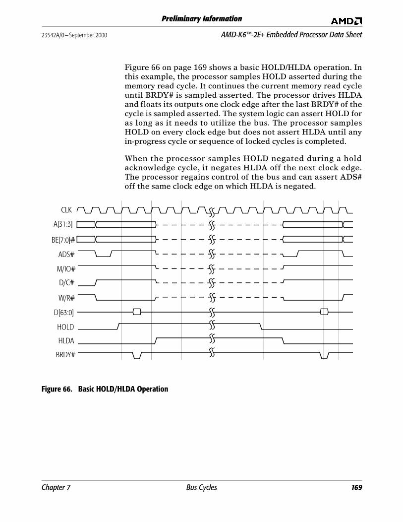
23542A/0—September 2000 AMD-K6™-2E+ Embedded Processor Data Sheet
Preliminary Information
Figure 66 on page 169 shows a basic HOLD/HLDA operation. Inthis example, the processor samples HOLD asserted during thememory read cycle. It continues the current memory read cycleuntil BRDY# is sampled asserted. The processor drives HLDAand floats its outputs one clock edge after the last BRDY# of thecycle is sampled asserted. The system logic can assert HOLD foras long as it needs to utilize the bus. The processor samplesHOLD on every clock edge but does not assert HLDA until anyin-progress cycle or sequence of locked cycles is completed.
When the processor samples HOLD negated during a holdacknowledge cycle, it negates HLDA off the next clock edge.The processor regains control of the bus and can assert ADS#off the same clock edge on which HLDA is negated.
Figure 66. Basic HOLD/HLDA Operation
CLK
A[31:3]
BE[7:0]#
ADS#
M/IO#
D/C#
W/R#
D[63:0]
HOLD
HLDA
BRDY#
Chapter 7 Bus Cycles 169

AMD-K6™-2E+ Embedded Processor Data Sheet 23542A/0—September 2000
Preliminary Information
HOLD-Initiated Inquire Hit to Shared or Exclusive Line
Figure 67 on page 171 shows a HOLD-initiated inquire cycle. Inthis example, the processor samples HOLD asserted during theburst memory read cycle. The processor completes the currentcycle (until the last expected BRDY# is sampled asserted),asserts HLDA and floats its outputs as described in “Hold andHold Acknowledge Cycle” on page 168.
The system logic drives an inquire cycle within the holdacknowledge cycle. It asserts EADS#, which validates theinquire address on A[31:5]. If EADS# is sampled assertedbefore HOLD is sampled negated, the processor recognizes it asa valid inquire cycle.
In Figure 67, the processor asserts HIT# and negates HITM# onthe clock edge after the clock edge on which EADS# is sampledasserted, indicating the current inquire cycle hit a shared orexclusive cache line. (Shared and exclusive cache lines have notbeen modified and do not need to be written back.) During aninquire cycle, the processor samples INV to determine whetherthe addressed cache line found in the processor’s cachestransitions to the invalid state or the shared state. In thisexample, the processor samples INV asserted with EADS#,which invalidates the cache line.
The system logic can negate HOLD off the same clock edge onwhich EADS# is sampled asserted. The processor continuesdriving HIT# in the same state until the next inquire cycle.HITM# is not asserted unless HIT# is asserted.
170 Bus Cycles Chapter 7
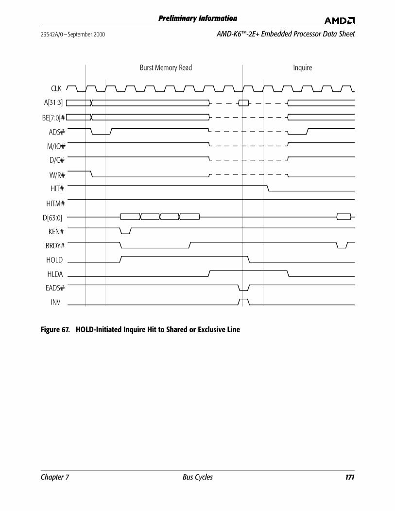
23542A/0—September 2000 AMD-K6™-2E+ Embedded Processor Data Sheet
Preliminary Information
Figure 67. HOLD-Initiated Inquire Hit to Shared or Exclusive Line
Burst Memory Read Inquire
CLK
A[31:3]
BE[7:0]#
ADS#
M/IO#
D/C#
W/R#
HIT#
HITM#
D[63:0]
KEN#
BRDY#
HOLD
HLDA
EADS#
INV
Chapter 7 Bus Cycles 171
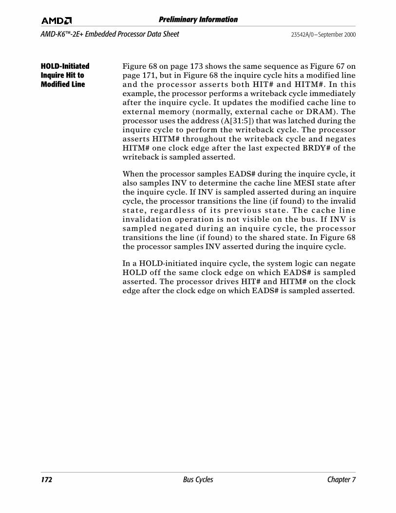
AMD-K6™-2E+ Embedded Processor Data Sheet 23542A/0—September 2000
Preliminary Information
HOLD-Initiated Inquire Hit to Modified Line
Figure 68 on page 173 shows the same sequence as Figure 67 onpage 171, but in Figure 68 the inquire cycle hits a modified lineand the processor asserts both HIT# and HITM#. In thisexample, the processor performs a writeback cycle immediatelyafter the inquire cycle. It updates the modified cache line toexternal memory (normally, external cache or DRAM). Theprocessor uses the address (A[31:5]) that was latched during theinquire cycle to perform the writeback cycle. The processorasserts HITM# throughout the writeback cycle and negatesHITM# one clock edge after the last expected BRDY# of thewriteback is sampled asserted.
When the processor samples EADS# during the inquire cycle, italso samples INV to determine the cache line MESI state afterthe inquire cycle. If INV is sampled asserted during an inquirecycle, the processor transitions the line (if found) to the invalidstate, regardless of its previous state. The cache lineinvalidation operation is not visible on the bus. If INV issampled negated during an inquire cycle, the processortransitions the line (if found) to the shared state. In Figure 68the processor samples INV asserted during the inquire cycle.
In a HOLD-initiated inquire cycle, the system logic can negateHOLD off the same clock edge on which EADS# is sampledasserted. The processor drives HIT# and HITM# on the clockedge after the clock edge on which EADS# is sampled asserted.
172 Bus Cycles Chapter 7
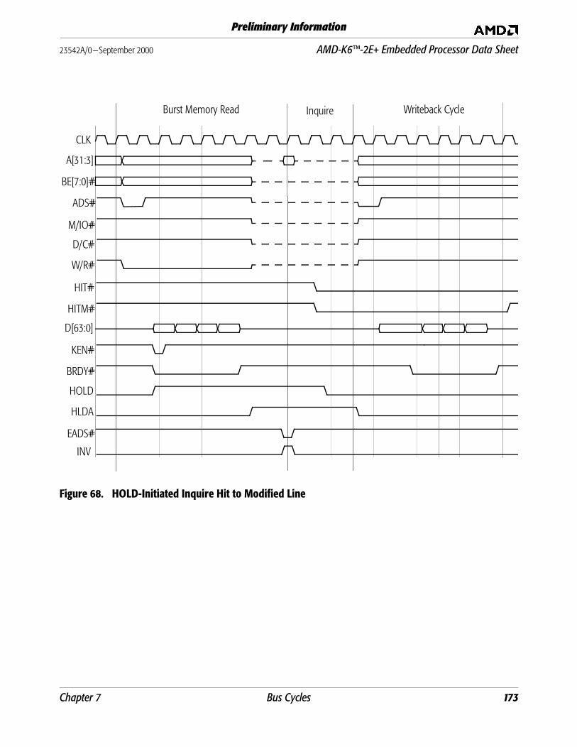
23542A/0—September 2000 AMD-K6™-2E+ Embedded Processor Data Sheet
Preliminary Information
Figure 68. HOLD-Initiated Inquire Hit to Modified Line
Burst Memory Read Inquire Writeback Cycle
CLK
A[31:3]
BE[7:0]#
ADS#
M/IO#
D/C#
W/R#
EADS#
HIT#
HITM#
D[63:0]
KEN#
BRDY#
HOLD
HLDA
INV
Chapter 7 Bus Cycles 173

AMD-K6™-2E+ Embedded Processor Data Sheet 23542A/0—September 2000
Preliminary Information
AHOLD-Initiated Inquire Miss
AHOLD can be asserted by the system to initiate one or moreinquire cycles. To allow the system to drive the address busduring an inquire cycle, the processor floats A[31:3] and AP offthe clock edge on which AHOLD is sampled asserted. The databus and all other control and status signals remain under thecontrol of the processor and are not floated. This functionalityallows a bus cycle in progress when AHOLD is sampled assertedto continue to completion. The processor resumes driving theaddress bus off the clock edge on which AHOLD is samplednegated.
In Figure 69 on page 175, the processor samples AHOLDasserted during the memory burst read cycle, and it floats theaddress bus off the same clock edge on which it samplesAHOLD asserted. While the processor still controls the bus, itcompletes the current cycle until the last expected BRDY# issampled asserted. The system logic drives EADS# with aninquire address on A[31:5] during an inquire cycle. Theprocessor samples EADS# asserted and compares the inquireaddress to its tag address in the L1 instruction and data caches,and in the L2 cache. In Figure 69, the inquire address misses thetag address in the processor (both HIT# and HITM# arenegated). Therefore, the processor proceeds to the next cyclewhen it samples AHOLD negated. (The processor can drive anew cycle by asserting ADS# off the same clock edge that itsamples AHOLD negated.)
For an AHOLD-initiated inquire cycle to be recognized, theprocessor must sample AHOLD asserted for at least twoconsecutive clocks before it samples EADS# asserted. If theprocessor detects an address parity error during an inquirecycle, APCHK# is asserted for one clock. The system logic mustrespond appropriately to the assertion of this signal.
174 Bus Cycles Chapter 7

23542A/0—September 2000 AMD-K6™-2E+ Embedded Processor Data Sheet
Preliminary Information
Figure 69. AHOLD-Initiated Inquire Miss
Read Inquire
CLK
A[31:3]
BE[7:0]#
AP
APCHK#
ADS#
HIT#
HITM#
D[63:0]
KEN#
BRDY#
AHOLD
EADS#
INV
Chapter 7 Bus Cycles 175

AMD-K6™-2E+ Embedded Processor Data Sheet 23542A/0—September 2000
Preliminary Information
AHOLD-Initiated Inquire Hit to Shared or Exclusive Line
In Figure 70 on page 177, the processor asserts HIT# andnegates HITM# off the clock edge after the clock edge on whichEADS# is sampled asserted, indicating the current inquirecycle hits either a shared or exclusive line. (HIT# is driven inthe same state until the next inquire cycle.) The processorsamples INV asserted during the inquire cycle and transitionsthe line to the invalid state regardless of its previous state.
During an AHOLD-initiated inquire cycle, the processorsamples AHOLD on every clock edge until it is negated. InFigure 70, the processor asserts ADS# off the same clock onwhich AHOLD is sampled negated. If the inquire cycle hits amodified line, the processor performs a writeback cycle beforeit drives a new bus cycle. The next section describes theAHOLD-initiated inquire cycle that hits a modified line.
176 Bus Cycles Chapter 7
23542A/0—September 2000 AMD-K6™-2E+ Embedded Processor Data Sheet
Preliminary Information
Figure 70. AHOLD-Initiated Inquire Hit to Shared or Exclusive Line
Burst Memory Read Inquire
CLK
A[31:3]
BE[7:0]#
ADS#
M/IO#
D/C#
W/R#
HIT#
HITM#
D[63:0]
KEN#
BRDY#
AHOLD
INV
EADS#
Chapter 7 Bus Cycles 177
AMD-K6™-2E+ Embedded Processor Data Sheet 23542A/0—September 2000
Preliminary Information
AHOLD-Initiated Inquire Hit to Modified Line
Figure 71 on page 179 shows an AHOLD-initiated inquire cyclethat hits a modified line. During the inquire cycle in thisexample, the processor asserts both HIT# and HITM# on theclock edge after the clock edge that it samples EADS# asserted.This condition indicates that the cache line exists in theprocessor’s L1 data cache or L2 cache in the modified state.
If the inquire cycle hits a modified line, the processor performsa writeback cycle immediately after the inquire cycle to updatethe modified cache line to shared memory (normally externalcache or DRAM). In Figure 71, the system logic holds AHOLDasserted throughout the inquire cycle and the processorwriteback cycle. In this case, the processor is not driving theaddress bus during the writeback cycle because AHOLD issampled asserted. The system logic writes the data to memoryby using its latched copy of the inquire cycle address. If theprocessor samples AHOLD negated before it performs thewriteback cycle, it drives the writeback cycle by using theaddress (A[31:5]) that it latched during the inquire cycle.
If INV is sampled asserted during an inquire cycle, theprocessor transitions the line (if found) to the invalid state,regardless of its previous state (the cache invalidationoperation is not visible on the bus). If INV is sampled negatedduring an inquire cycle, the processor transitions the line (iffound) to the shared state. In either case, if the line is found inthe modified state, the processor writes it back to memorybefore changing its state. Figure 71 shows that the processorsamples INV asserted during the inquire cycle and invalidatesthe cache line after the inquire cycle.
178 Bus Cycles Chapter 7
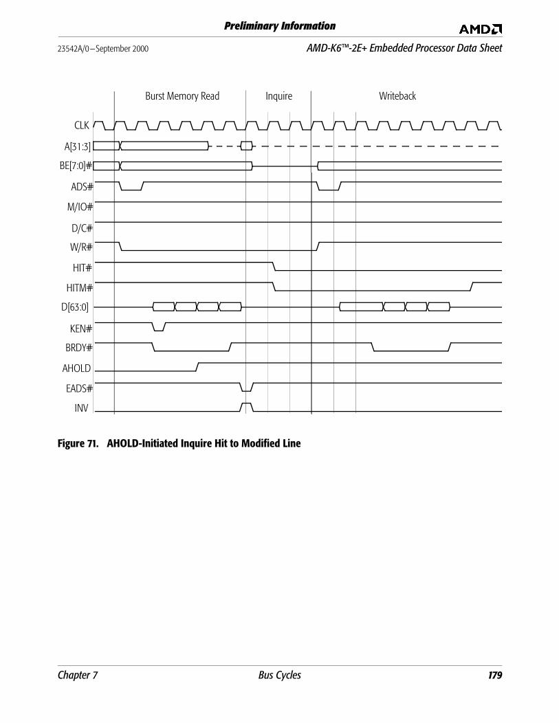
23542A/0—September 2000 AMD-K6™-2E+ Embedded Processor Data Sheet
Preliminary Information
Figure 71. AHOLD-Initiated Inquire Hit to Modified Line
Burst Memory Read Inquire Writeback
CLK
A[31:3]
BE[7:0]#
ADS#
M/IO#
D/C#
W/R#
HIT#
HITM#
D[63:0]
KEN#
BRDY#
AHOLD
EADS#
INV
Chapter 7 Bus Cycles 179
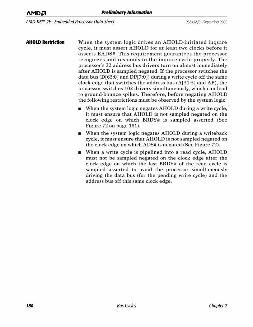
AMD-K6™-2E+ Embedded Processor Data Sheet 23542A/0—September 2000
Preliminary Information
AHOLD Restriction When the system logic drives an AHOLD-initiated inquirecycle, it must assert AHOLD for at least two clocks before itasserts EADS#. This requirement guarantees the processorrecognizes and responds to the inquire cycle properly. Theprocessor’s 32 address bus drivers turn on almost immediatelyafter AHOLD is sampled negated. If the processor switches thedata bus (D[63:0] and DP[7:0]) during a write cycle off the sameclock edge that switches the address bus (A[31:3] and AP), theprocessor switches 102 drivers simultaneously, which can leadto ground-bounce spikes. Therefore, before negating AHOLDthe following restrictions must be observed by the system logic:
■ When the system logic negates AHOLD during a write cycle,it must ensure that AHOLD is not sampled negated on theclock edge on which BRDY# is sampled asserted (SeeFigure 72 on page 181).
■ When the system logic negates AHOLD during a writebackcycle, it must ensure that AHOLD is not sampled negated onthe clock edge on which ADS# is negated (See Figure 72).
■ When a write cycle is pipelined into a read cycle, AHOLDmust not be sampled negated on the clock edge after theclock edge on which the last BRDY# of the read cycle issampled asserted to avoid the processor simultaneouslydriving the data bus (for the pending write cycle) and theaddress bus off this same clock edge.
180 Bus Cycles Chapter 7
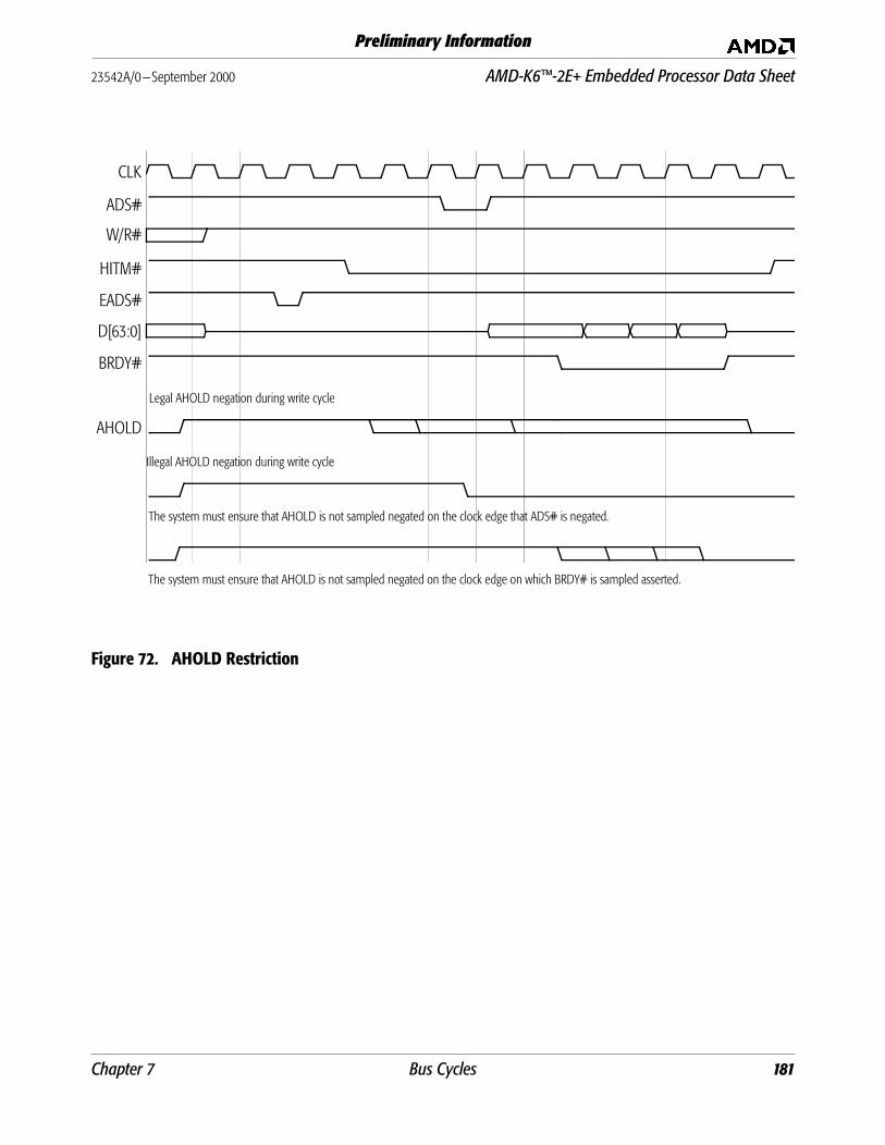
23542A/0—September 2000 AMD-K6™-2E+ Embedded Processor Data Sheet
Preliminary Information
Figure 72. AHOLD Restriction
The system must ensure that AHOLD is not sampled negated on the clock edge that ADS# is negated.
Legal AHOLD negation during write cycle
Illegal AHOLD negation during write cycle
CLK
ADS#
W/R#
HITM#
EADS#
D[63:0]
BRDY#
AHOLD
The system must ensure that AHOLD is not sampled negated on the clock edge on which BRDY# is sampled asserted.
Chapter 7 Bus Cycles 181
AMD-K6™-2E+ Embedded Processor Data Sheet 23542A/0—September 2000
Preliminary Information
Bus Backoff (BOFF#) BOFF# provides the fastest response among bus-hold inputs.Either the system logic or another bus master can assert BOFF#to gain control of the bus immediately. BOFF# is also used toresolve potential deadlock problems that arise as a result ofinquire cycles. The processor samples BOFF# on every clockedge. I f BOFF# i s sampled asserted , the processorunconditionally aborts any cycles in progress and transitions toa bus hold state. (See “BOFF# (Backoff)” on page 102.)Figure 73 on page 183 shows a read cycle that is aborted whenthe processor samples BOFF# asserted even though BRDY# issampled asserted on the same clock edge. The read cycle isrestarted after BOFF# is sampled negated (KEN# must be inthe same state during the restarted cycle as its state during theaborted cycle).
During a BOFF#-initiated inquire cycle that hits a shared orexclusive line, the processor samples BOFF# negated andrestarts any bus cycle that was aborted when BOFF# wasasserted. If a BOFF#-initiated inquire cycle hits a modified line,the processor performs a writeback cycle before it restarts theaborted cycle.
If the processor samples BOFF# asserted on the same clockedge that it asserts ADS#, ADS# is floated but the system logicmay erroneously interpret ADS# as asserted. In this case, thesystem logic must properly interpret the state of ADS# whenBOFF# is negated.
182 Bus Cycles Chapter 7

23542A/0—September 2000 AMD-K6™-2E+ Embedded Processor Data Sheet
Preliminary Information
Figure 73. BOFF# Timing
Read Backoff Cycle Restart Read Cycle
CLK
A[31:3]
BE[7:0]#
ADS#
M/IO#
D/C#
W/R#
BOFF#
D[63:0]
BRDY#
Chapter 7 Bus Cycles 183

AMD-K6™-2E+ Embedded Processor Data Sheet 23542A/0—September 2000
Preliminary Information
Locked Cycles The processor asserts LOCK# during a sequence of bus cycles toensure the cycles are completed without allowing other busmasters to intervene. Locked operations can consist of two tofive cycles. LOCK# is asserted during the following operations:
■ An interrupt acknowledge sequence
■ Descriptor Table accesses
■ Page Directory and Page Table accesses
■ XCHG instruction
■ An instruction with an allowable LOCK prefix
In order to ensure that locked operations appear on the bus andare visible to the entire system, any data operands addressedduring a locked cycle that reside in the processor’s caches areflushed and invalidated from the caches prior to the lockedoperation. If the cache line is in the modified state, it is writtenback and invalidated prior to the locked operation. Likewise,any data read during a locked operation is not cached. Theprocessor negates LOCK# for at least one clock betweenconsecutive sequences of locked operations to allow the systemlogic to arbitrate for the bus.
The processor asserts SCYC during misaligned locked transferson the D[63:0] data bus. The processor generates additional buscycles to complete the transfer of misaligned data.
Basic Locked Operation
Figure 74 on page 185 shows a pair of read-write bus cycles. Itrepresents a typical read-modify-write locked operation. Theprocessor asserts LOCK# off the same clock edge that it assertsADS# of the first bus cycle in the locked operation and holds itasserted until the last expected BRDY# of the last bus cycle inthe locked operation is sampled asserted. (The processornegates LOCK# off of the same clock edge.)
184 Bus Cycles Chapter 7
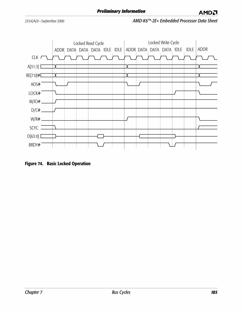
23542A/0—September 2000 AMD-K6™-2E+ Embedded Processor Data Sheet
Preliminary Information
Figure 74. Basic Locked Operation
Locked Read Cycle Locked Write Cycle
CLK
A[31:3]
BE[7:0]#
ADS#
LOCK#
M/IO#
D/C#
W/R#
D[63:0]
BRDY#
ADDR DATA DATA DATA IDLE IDLE ADDR DATA DATA DATA IDLE IDLE ADDR
SCYC
Chapter 7 Bus Cycles 185
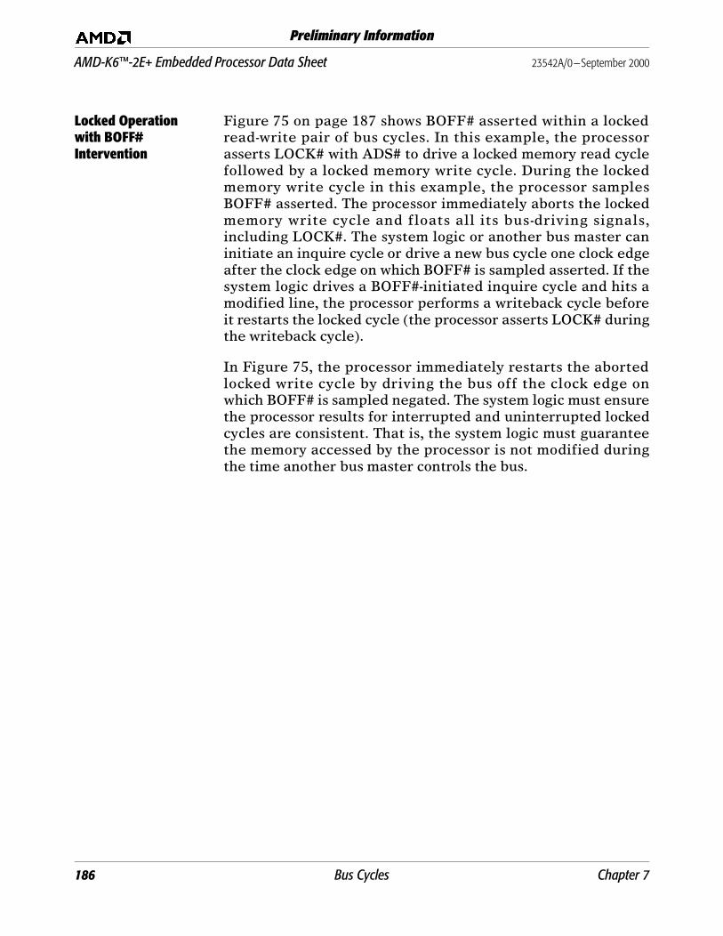
AMD-K6™-2E+ Embedded Processor Data Sheet 23542A/0—September 2000
Preliminary Information
Locked Operation with BOFF# Intervention
Figure 75 on page 187 shows BOFF# asserted within a lockedread-write pair of bus cycles. In this example, the processorasserts LOCK# with ADS# to drive a locked memory read cyclefollowed by a locked memory write cycle. During the lockedmemory write cycle in this example, the processor samplesBOFF# asserted. The processor immediately aborts the lockedmemory write cycle and floats all its bus-driving signals,including LOCK#. The system logic or another bus master caninitiate an inquire cycle or drive a new bus cycle one clock edgeafter the clock edge on which BOFF# is sampled asserted. If thesystem logic drives a BOFF#-initiated inquire cycle and hits amodified line, the processor performs a writeback cycle beforeit restarts the locked cycle (the processor asserts LOCK# duringthe writeback cycle).
In Figure 75, the processor immediately restarts the abortedlocked write cycle by driving the bus off the clock edge onwhich BOFF# is sampled negated. The system logic must ensurethe processor results for interrupted and uninterrupted lockedcycles are consistent. That is, the system logic must guaranteethe memory accessed by the processor is not modified duringthe time another bus master controls the bus.
186 Bus Cycles Chapter 7
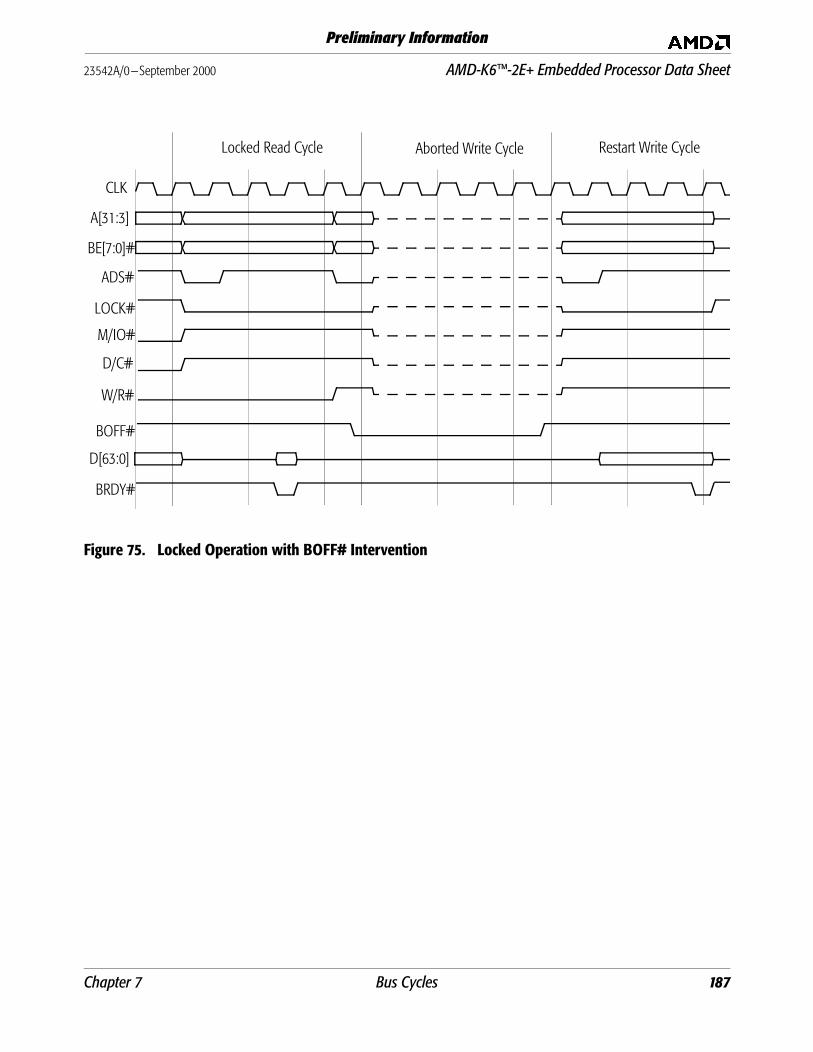
23542A/0—September 2000 AMD-K6™-2E+ Embedded Processor Data Sheet
Preliminary Information
Figure 75. Locked Operation with BOFF# Intervention
Locked Read Cycle Aborted Write Cycle Restart Write Cycle
CLK
A[31:3]
BE[7:0]#
ADS#
LOCK#
M/IO#
D/C#
W/R#
BOFF#
D[63:0]
BRDY#
Chapter 7 Bus Cycles 187

AMD-K6™-2E+ Embedded Processor Data Sheet 23542A/0—September 2000
Preliminary Information
Interrupt Acknowledge
In response to recognizing the system’s maskable interrupt(INTR), the processor drives an interrupt acknowledge cycle atthe next instruct ion boundary. During an interruptacknowledge cycle, the processor drives a locked pair of readcycles as shown in Figure 76 on page 189. The first read cycle isnot functional, and the second read cycle returns the interruptnumber on D[7:0] (00h–FFh). Table 32 shows the state of thesignals during an interrupt acknowledge cycle.
The system logic can drive INTR either synchronously orasynchronously. If it is asserted asynchronously, it must beasserted for a minimum pulse width of two clocks. To ensure itis recognized, INTR must remain asserted until an interruptacknowledge sequence is complete.
Table 32. Interrupt Acknowledge Operation Definition
Processor Outputs First Bus Cycle Second Bus CycleD/C# Low Low
M/IO# Low Low
W/R# Low Low
BE[7:0]# EFh FEh (low byte enabled)
A[31:3] 0000_0000h 0000_0000h
D[63:0] (ignored)Interrupt number expected from interrupt con-troller on D[7:0]
188 Bus Cycles Chapter 7
23542A/0—September 2000 AMD-K6™-2E+ Embedded Processor Data Sheet
Preliminary Information
Figure 76. Interrupt Acknowledge Operation
Interrupt Acknowledge Cycles
Interrupt Number
CLK
A[31:3]
BE[7:0]#
ADS#
M/IO#
D/C#
W/R#
LOCK#
INTR
D[63:0]
KEN#
BRDY#
Chapter 7 Bus Cycles 189
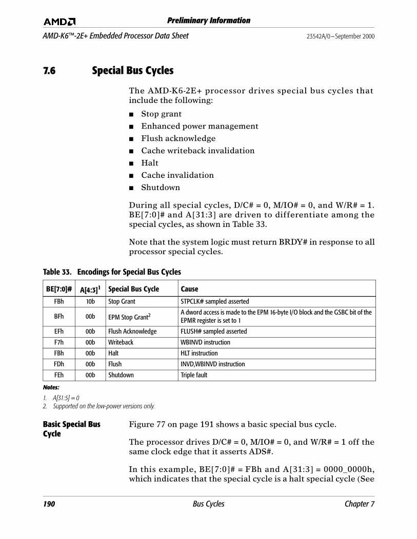
AMD-K6™-2E+ Embedded Processor Data Sheet 23542A/0—September 2000
Preliminary Information
7.6 Special Bus Cycles
The AMD-K6-2E+ processor drives special bus cycles thatinclude the following:
■ Stop grant
■ Enhanced power management
■ Flush acknowledge
■ Cache writeback invalidation
■ Halt
■ Cache invalidation
■ Shutdown
During all special cycles, D/C# = 0, M/IO# = 0, and W/R# = 1.BE[7:0]# and A[31:3] are driven to differentiate among thespecial cycles, as shown in Table 33.
Note that the system logic must return BRDY# in response to allprocessor special cycles.
Basic Special Bus Cycle
Figure 77 on page 191 shows a basic special bus cycle.
The processor drives D/C# = 0, M/IO# = 0, and W/R# = 1 off thesame clock edge that it asserts ADS#.
In this example, BE[7:0]# = FBh and A[31:3] = 0000_0000h,which indicates that the special cycle is a halt special cycle (See
Table 33. Encodings for Special Bus Cycles
BE[7:0]# A[4:3]1
Notes:
1. A[31:5] = 0
Special Bus Cycle Cause
FBh 10b Stop Grant STPCLK# sampled asserted
BFh 00b EPM Stop Grant2
2. Supported on the low-power versions only.
A dword access is made to the EPM 16-byte I/O block and the GSBC bit of the EPMR register is set to 1
EFh 00b Flush Acknowledge FLUSH# sampled asserted
F7h 00b Writeback WBINVD instruction
FBh 00b Halt HLT instruction
FDh 00b Flush INVD,WBINVD instruction
FEh 00b Shutdown Triple fault
190 Bus Cycles Chapter 7
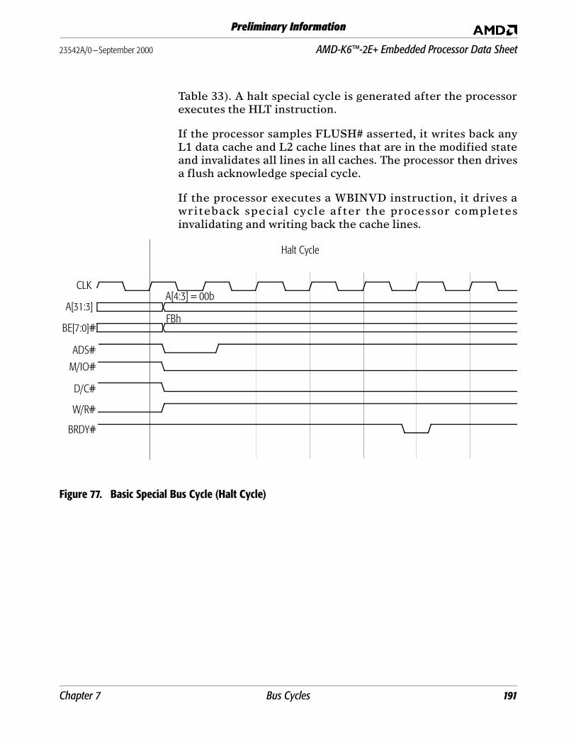
23542A/0—September 2000 AMD-K6™-2E+ Embedded Processor Data Sheet
Preliminary Information
Table 33). A halt special cycle is generated after the processorexecutes the HLT instruction.
If the processor samples FLUSH# asserted, it writes back anyL1 data cache and L2 cache lines that are in the modified stateand invalidates all lines in all caches. The processor then drivesa flush acknowledge special cycle.
If the processor executes a WBINVD instruction, it drives awriteback special cycle after the processor completesinvalidating and writing back the cache lines.
Figure 77. Basic Special Bus Cycle (Halt Cycle)
Halt Cycle
A[4:3] = 00b
FBh
CLK
A[31:3]
BE[7:0]#
ADS#
M/IO#
D/C#
W/R#
BRDY#
Chapter 7 Bus Cycles 191

AMD-K6™-2E+ Embedded Processor Data Sheet 23542A/0—September 2000
Preliminary Information
Shutdown Cycle In Figure 78 on page 192, a shutdown (triple fault) occurs in thefirst half of the waveform, and a shutdown special cycle followsin the second half. The processor enters shutdown when aninterrupt or exception occurs during the handling of a doublefault (INT 8), which amounts to a triple fault. When theprocessor encounters a triple fault, it stops its activity on thebus and generates the shutdown special bus cycle (BE[7:0]# =FEh).
The system logic must assert NMI, INIT, RESET, or SMI# to getthe processor out of the shutdown state.
Figure 78. Shutdown Cycle
Shutdown Occurs(Triple Fault)
Shutdown Special Cycle
CLK
A[31:3]
BE[7:0]#
ADS#
LOCK#
M/IO#
D/C#
W/R#
D[63:0]
KEN#
BRDY#
A[4:3] = 00b
FEh
192 Bus Cycles Chapter 7
23542A/0—September 2000 AMD-K6™-2E+ Embedded Processor Data Sheet
Preliminary Information
Stop Grant and Stop Clock States
Figure 79 on page 194 and Figure 80 on page 195 show theprocessor transition from normal execution to the Stop Grantstate, then to the Stop Clock state, back to the Stop Grant state,and finally back to normal execution. The series of transitionsbegins when the processor samples STPCLK# asserted. Onrecognizing a STPCLK# interrupt at the next instructionretirement boundary, the processor performs the followingactions, in the order shown:
1. Its instruction pipelines are flushed.
2. All pending and in-progress bus cycles are completed.
3. The STPCLK# assertion is acknowledged by executing aStop Grant special bus cycle.
4. Its internal clock is stopped after BRDY# of the Stop Grantspecial bus cycle is sampled asserted (if EWBE# is maskedoff, then entry into the Stop Grant state is not affected byEWBE#) and after EWBE# is sampled asserted.
5. The Stop Clock state is entered if the system logic stops thebus clock CLK (optional).
STPCLK# is sampled as a level-sensitive input on every clockedge but is not recognized until the next instruction boundary.The system logic drives the signal either synchronously orasynchronously. If it is asserted asynchronously, it must beasserted for a minimum pulse width of two clocks. STPCLK#must remain asserted until recognized, which is indicated bythe completion of the Stop Grant special cycle.
Chapter 7 Bus Cycles 193
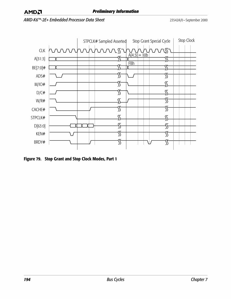
AMD-K6™-2E+ Embedded Processor Data Sheet 23542A/0—September 2000
Preliminary Information
Figure 79. Stop Grant and Stop Clock Modes, Part 1
STPCLK# Sampled Asserted Stop Grant Special Cycle
CLK
A[31:3]
BE[7:0]#
ADS#
M/IO#
D/C#
W/R#
CACHE#
STPCLK#
D[63:0]
KEN#
BRDY#
Stop Clock
A[4:3] = 10b
FBh
194 Bus Cycles Chapter 7
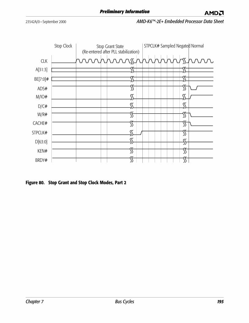
23542A/0—September 2000 AMD-K6™-2E+ Embedded Processor Data Sheet
Preliminary Information
Figure 80. Stop Grant and Stop Clock Modes, Part 2
Stop Grant State(Re-entered after PLL stabilization)
STPCLK# Sampled Negated NormalStop Clock
CLK
A[31:3]
BE[7:0]#
ADS#
M/IO#
D/C#
W/R#
CACHE#
STPCLK#
D[63:0]
KEN#
BRDY#
Chapter 7 Bus Cycles 195

AMD-K6™-2E+ Embedded Processor Data Sheet 23542A/0—September 2000
Preliminary Information
INIT-Initiated Transition from Protected Mode to Real Mode
INIT is typically asserted in response to a BIOS interrupt thatwrites to an I/O port. This interrupt is often in response to aCtrl-Alt-Del keyboard input. The BIOS writes to a port (similarto port 64h in the keyboard controller) that asserts INIT. INIT isalso used to support 80286 software that must return to Realmode after accessing extended memory in Protected mode.
The assertion of INIT causes the processor to empty itspipelines, initialize most of its internal state, and branch toaddress FFFF_FFF0h—the same instruction execution startingpoint used after RESET. Unlike RESET, the processorpreserves the contents of its caches, the floating-point state, theMMX state, Model-Specific Registers (MSRs), the CD and NWbits of the CR0 register, the time stamp counter, and otherspecific internal resources.
Figure 81 on page 197 shows an example in which the operatingsystem writes to an I/O port, causing the system logic to assertINIT. The sampling of INIT asserted starts an extendedmicrocode sequence that terminates with a code fetch fromFFFF_FFF0h, the reset location. INIT is sampled on every clockedge but is not recognized until the next instruction boundary.During an I/O write cycle, it must be sampled asserted aminimum of three clock edges before BRDY# is sampledasserted if it is to be recognized on the boundary between theI/O write instruction and the following instruction. If INIT isasserted synchronously, it can be asserted for a minimum of oneclock. If it is asserted asynchronously, it must have beennegated for a minimum of two clocks, followed by an assertionof a minimum of two clocks.
196 Bus Cycles Chapter 7
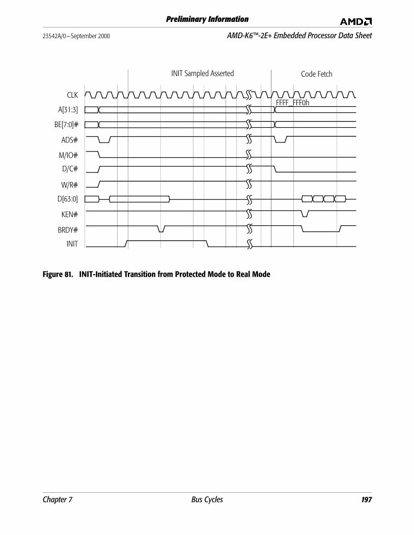
23542A/0—September 2000 AMD-K6™-2E+ Embedded Processor Data Sheet
Preliminary Information
Figure 81. INIT-Initiated Transition from Protected Mode to Real Mode
Code Fetch
FFFF_FFF0h
INIT Sampled Asserted
CLK
A[31:3]
BE[7:0]#
ADS#
M/IO#
D/C#
W/R#
D[63:0]
KEN#
BRDY#
INIT
Chapter 7 Bus Cycles 197

AMD-K6™-2E+ Embedded Processor Data Sheet 23542A/0—September 2000
Preliminary Information
198 Bus Cycles Chapter 7
23542A/0—September 2000 AMD-K6™-2E+ Embedded Processor Data Sheet
Preliminary Information
8 Power-on Configuration and Initialization
On power-on the system logic must reset the AMD-K6-2E+processor by asserting the RESET signal. When the processorsamples RESET asserted, it immediately flushes and initializesall internal resources and its internal state, including itspipelines and caches, the floating-point state, the MMX and3DNow! states, and all registers. Then the processor jumps toaddress FFFF_FFF0h to start instruction execution.
8.1 Signals Sampled During the Falling Transition of RESET
FLUSH# FLUSH# is sampled on the falling transition of RESET todetermine if the processor begins normal instruction executionor enters Three-State Test mode.
■ If FLUSH# is High during the falling transition of RESET,the processor unconditionally runs its Built-In Self Test(BIST), performs the normal reset functions, then jumps toaddress FFFF_FFF0h to start instruction execution. (See“Built-In Self-Test (BIST)” on page 251 for more details.)
■ If FLUSH# is Low during the falling transition of RESET,the processor enters Three-State Test mode. (See“Three-State Test Mode” on page 252 and “FLUSH# (CacheFlush)” on page 112 for more details.)
BF[2:0] The internal operating frequency of the processor isdetermined by the state of the bus frequency signals BF[2:0]when they are sampled during the falling transition of RESET.The frequency of the CLK input signal is multiplied internallyby a ratio defined by BF[2:0]. (See “BF[2:0] (Bus Frequency)”on page 101 for the processor-clock to bus-clock ratios.)
Chapter 8 Power-on Configuration and Initialization 199
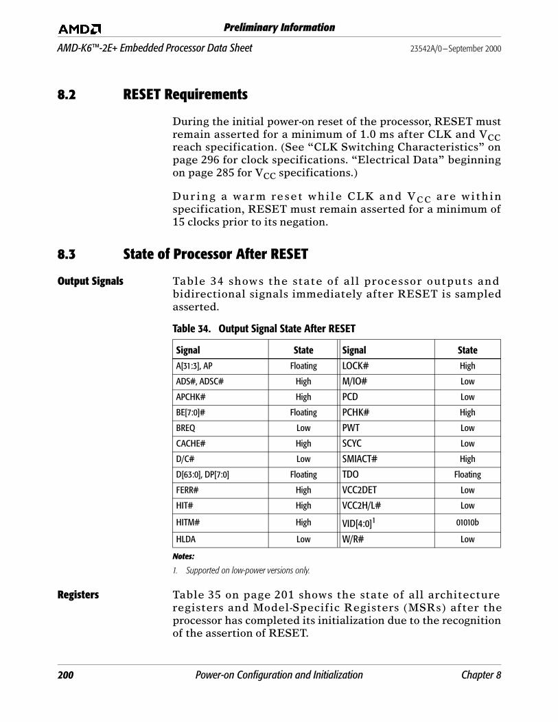
AMD-K6™-2E+ Embedded Processor Data Sheet 23542A/0—September 2000
Preliminary Information
8.2 RESET Requirements
During the initial power-on reset of the processor, RESET mustremain asserted for a minimum of 1.0 ms after CLK and VCCreach specification. (See “CLK Switching Characteristics” onpage 296 for clock specifications. “Electrical Data” beginningon page 285 for VCC specifications.)
During a warm reset while CLK and VC C are withinspecification, RESET must remain asserted for a minimum of15 clocks prior to its negation.
8.3 State of Processor After RESET
Output Signals Table 34 shows the state of all processor outputs andbidirectional signals immediately after RESET is sampledasserted.
Registers Table 35 on page 201 shows the state of all architectureregisters and Model-Specific Registers (MSRs) after theprocessor has completed its initialization due to the recognitionof the assertion of RESET.
Table 34. Output Signal State After RESET
Signal State Signal State
A[31:3], AP Floating LOCK# High
ADS#, ADSC# High M/IO# Low
APCHK# High PCD Low
BE[7:0]# Floating PCHK# High
BREQ Low PWT Low
CACHE# High SCYC Low
D/C# Low SMIACT# High
D[63:0], DP[7:0] Floating TDO Floating
FERR# High VCC2DET Low
HIT# High VCC2H/L# Low
HITM# High VID[4:0]1
Notes:
1. Supported on low-power versions only.
01010b
HLDA Low W/R# Low
200 Power-on Configuration and Initialization Chapter 8
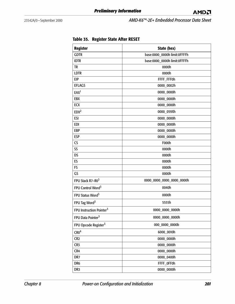
23542A/0—September 2000 AMD-K6™-2E+ Embedded Processor Data Sheet
Preliminary Information
Table 35. Register State After RESET
Register State (hex)GDTR base:0000_0000h limit:0FFFFh
IDTR base:0000_0000h limit:0FFFFh
TR 0000h
LDTR 0000h
EIP FFFF_FFF0h
EFLAGS 0000_0002h
EAX1 0000_0000h
EBX 0000_0000h
ECX 0000_0000h
EDX2 0000_059Xh
ESI 0000_0000h
EDI 0000_0000h
EBP 0000_0000h
ESP 0000_0000h
CS F000h
SS 0000h
DS 0000h
ES 0000h
FS 0000h
GS 0000h
FPU Stack R7–R03 0000_0000_0000_0000_0000h
FPU Control Word3 0040h
FPU Status Word3 0000h
FPU Tag Word3 5555h
FPU Instruction Pointer3 0000_0000_0000h
FPU Data Pointer3 0000_0000_0000h
FPU Opcode Register3 000_0000_0000b
CR04 6000_0010h
CR2 0000_0000h
CR3 0000_0000h
CR4 0000_0000h
DR7 0000_0400h
DR6 FFFF_0FF0h
DR3 0000_0000h
Chapter 8 Power-on Configuration and Initialization 201

AMD-K6™-2E+ Embedded Processor Data Sheet 23542A/0—September 2000
Preliminary Information
DR2 0000_0000h
DR1 0000_0000h
DR0 0000_0000h
MCAR3 0000_0000_0000_0000h
MCTR3 0000_0000_0000_0000h
TR123 0000_0000_0000_0000h
TSC3 0000_0000_0000_0000h
EFER3 0000_0000_0000_0002h
STAR3 0000_0000_0000_0000h
WHCR3 0000_0000_0000_0000h
UWCCR3 0000_0000_0000_0000h
PSOR5 0000_0000_0000_01SBh
PFIR3,5 0000_0000_0000_0000h
EPMR3,6 0000_0000_0000_0000h
Notes:
1. The contents of EAX indicate if BIST was successful. If EAX = 0000_0000h, BIST was successful.If EAX is non-zero, BIST failed.
2. EDX contains the AMD-K6-2E+ processor signature, where X indicates the processor Stepping ID.3. The contents of these registers are preserved following the recognition of INIT.4. The CD and NW bits of CR0 are preserved following the recognition of INIT.5. “S” represents the Stepping. “B” represents PSOR[3:0], where PSOR[3] equals 0, and PSOR[2:0] is
equal to the value of the BF[2:0] signals sampled during the falling transition of RESET.6. Supported on low-power versions only.
Table 35. Register State After RESET (continued)
Register State (hex)
202 Power-on Configuration and Initialization Chapter 8
23542A/0—September 2000 AMD-K6™-2E+ Embedded Processor Data Sheet
Preliminary Information
8.4 State of Processor After INIT
The recognition of the assertion of INIT causes the processor toempty its pipelines, to initialize most of its internal state, and tobranch to address FFFF_FFF0h—the same instructionexecution starting point used after RESET.
Unlike RESET, the processor preserves the contents of itscaches, the floating-point state, the MMX and 3DNow! states,MSRs, and the CD and NW bits of the CR0 register.
The edge-sensitive interrupts FLUSH# and SMI# are sampledand preserved during the INIT process and are handledaccordingly after the initialization is complete. However, theprocessor resets any pending NMI interrupt upon samplingINIT asserted.
INIT can be used as an accelerator for 80286 code that requiresa reset to exit from Protected mode back to Real mode.
Chapter 8 Power-on Configuration and Initialization 203

AMD-K6™-2E+ Embedded Processor Data Sheet 23542A/0—September 2000
Preliminary Information
204 Power-on Configuration and Initialization Chapter 8

23542A/0—September 2000 AMD-K6™-2E+ Embedded Processor Data Sheet
Preliminary Information
9 Cache Organization
The following sections describe the basic architecture andresources of the AMD-K6-2E+ processor internal caches.
The performance of the AMD-K6-2E+ processor is enhanced bywriteback level-one (L1) and level-two (L2) caches.
■ The L1 cache is organized as separate 32-Kbyte instructionand data caches, each with two-way set associativity.
■ The L2 cache is 128 Kbytes, and is organized as a unified,four-way set-associative cache (See Figure 82 on page 206).
The cache line size is 32 bytes, and lines are fetched fromexternal memory using an efficient pipelined burst transaction.
As the L1 instruction cache is filled from the L2 cache or fromexternal memory, each instruction byte is analyzed forinstruction boundaries using predecode logic. Predecodingannotates each instruction byte in the L1 instruction cache withinformation that later enables the decoders to efficientlydecode multiple instructions simultaneously.
Translation lookaside buffers (TLB) are used in conjunctionwith the L1 cache to translate linear addresses to physicaladdresses. The L1 instruction cache is associated with a64-entry TLB, while the L1 data cache is associated with a128-entry TLB.
Chapter 9 Cache Organization 205
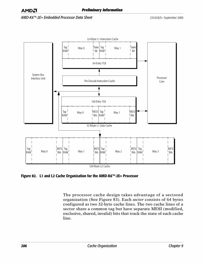
AMD-K6™-2E+ Embedded Processor Data Sheet 23542A/0—September 2000
Preliminary Information
Figure 82. L1 and L2 Cache Organization for the AMD-K6™-2E+ Processor
The processor cache design takes advantage of a sectoredorganization (See Figure 83). Each sector consists of 64 bytesconfigured as two 32-byte cache lines. The two cache lines of asector share a common tag but have separate MESI (modified,exclusive, shared, invalid) bits that track the state of each cacheline.
ProcessorCore
System Bus Interface Unit
128-Entry TLB
64-Entry TLB
StateBit
TagRAM
Way 0 Way 1 StateBit
TagRAM
32-Kbyte L1 Instruction Cache
32-Kbyte L1 Data Cache
Pre-Decode Instruction Cache
MESIBits
TagRAM
Way 0 Way 1 MESIBits
TagRAM
128-Kbyte L2 Cache
MESIBits
TagRAM Way 0 Way 1
MESIBits
TagRAM
MESIBits
TagRAM Way 2 Way 3
MESIBits
TagRAM
206 Cache Organization Chapter 9

23542A/0—September 2000 AMD-K6™-2E+ Embedded Processor Data Sheet
Preliminary Information
L1 Instruction Cache Line
L1 Data Cache Line and L2 Cache Line
Note: L1 instruction-cache lines have only two coherency states(valid or invalid) rather than the four MESI coherencystates of L1 data-cache and L2 cache lines. Only two statesare needed for the L1 instruction cache because these linesare read-only.
Figure 83. L1 Cache Sector Organization
9.1 MESI States in the L1 Data Cache and L2 Cache
The state of each line in the caches is tracked by the MESI bits.The coherency of these states or MESI bits is maintained byinternal processor snoops and external inquire cycles by thesystem logic. The following four states are defined for the L1data cache and the L2 cache:
■ Modified—This line has been modified and is different fromexternal memory.
■ Exclusive—In general, an exclusive line in the L1 data cacheor the L2 cache is not modified and is the same as externalmemory. The exception is the case where a line exists in themodified state in the L1 data cache and also resides in theL2 cache. By design, the line in the L2 cache must be in theexclusive state.
■ Shared—If a cache line is in the shared state it means thatthe same line can exist in more than one cache system.
■ Invalid—The information in this line is not valid.
TagAddress
Cache Line 0 Byte 31 Predecode Bits Byte 30 Predecode Bits ........ ........ Byte 0 Predecode Bits 1 MESI Bit
Cache Line 1 Byte 31 Predecode Bits Byte 30 Predecode Bits ........ ........ Byte 0 Predecode Bits 1 MESI Bit
TagAddress
Cache Line 0 Byte 31 Byte 30 ........ ........ Byte 0 2 MESI Bits
Cache Line 1 Byte 31 Byte 30 ........ ........ Byte 0 2 MESI Bits
Chapter 9 Cache Organization 207
AMD-K6™-2E+ Embedded Processor Data Sheet 23542A/0—September 2000
Preliminary Information
9.2 Predecode Bits
Decoding x86 instructions is particularly difficult because theinstructions vary in length, ranging from 1 to 15 bytes long.Predecode logic supplies the predecode bits associated witheach instruction byte.
Predecode bits indicate the number of bytes to the start of thenext x86 instruction. The predecode bits are passed with theinstruction bytes to the decoders where they assist with parallelx86 instruction decoding. The predecode bits use memoryseparate from the 32-Kbyte L1 instruction cache. Thepredecode bits are stored in an extended L1 instruction cachealongside each x86 instruction byte as shown in Figure 83 onpage 207.
The L2 cache does not store predecode bits. As an instructioncache line is fetched from the L2 cache, the predecode bits aregenerated and stored alongside the cache line in the L1instruction cache in the same manner as if the cache line werefetched from the processor’s system bus.
9.3 Cache Operation
The operating modes for the caches are configured by softwareusing the not writethrough (NW) and cache disable (CD) bits ofcontrol register 0 (CR0 bits 29 and 30, respectively). These bitsare used in all operating modes.
■ When the CD and NW bits are both set to 0, the cache is fullyenabled. This is the standard operating mode for the cache.If a L1 cache read miss occurs, the processor determines ifthe read hits the L2 cache, in which case the cache line issupplied from the L2 cache to the L1 cache. If a read missesboth the L1 and the L2 caches, a line fill (32-byte burst read)on the system bus occurs in order to fetch the cache line. Thecache line is then filled in both the L1 and the L2 caches.Write hits to the L1 and L2 caches are updated, while writemisses and writes to shared lines cause external memoryupdates. Refer to Table 39 on page 221 for a summary ofcache read and write cycles and the effect of theseoperations on the cache MESI state.
Note: A write allocate operation can modify the behavior of writemisses to the caches. See “Write Allocate” on page 215.
208 Cache Organization Chapter 9
23542A/0—September 2000 AMD-K6™-2E+ Embedded Processor Data Sheet
Preliminary Information
The AMD-K6-2E+ processor does not enforce any rules ofinclusion or exclusion as part of the protocol defined for theL1 and L2 caches. However, there are certain restrictionsimposed by design on the allowable MESI states of a cacheline that exists in both the L1 cache and the L2 cache. Referto Table 40 on page 225 for a list of the valid cache-linestates allowed.
■ When CD is set to 0 and NW is set to 1, an invalid mode ofoperation exists that causes a general protection fault tooccur.
■ When CD is set to 1 (disabled) and NW is set to 0, the cachefill mechanism is disabled but the contents of the cache arestill valid. The processor reads from the caches if the readhits the L1 or the L2 cache. If a read misses both the L1 andthe L2 caches, a line fill does not occur on the system bus.Write hits to the L1 or L2 cache are updated, while writemisses and writes to shared lines cause external memoryupdates. If PWT is driven Low and WB/WT# is sampledHigh, a write hit to a shared line changes the cache-line stateto exclusive.
■ When the CD and NW bits are both set to 1, the cache is fullydisabled. Even though the cache is disabled, the contentsare not necessarily invalid. The processor reads from thecaches if the read hits the L1 or the L2 cache. If a readmisses both the L1 and the L2 caches, a line fill does notoccur on the system bus. If a write hits the L1 or the L2cache, the cache is updated but an external memory updatedoes not occur. If a cache line is in the exclusive state duringa write hit, the cache-line state is changed to modified.Cache lines in the shared state remain in the shared stateafter a write hit. Write misses access external memorydirectly.
The operating system can control the cacheability of a page.The paging mechanism is controlled by CR3, the Page DirectoryEntry (PDE), and the Page Table Entry (PTE). Within CR3,PDE, and PTE are Page Cache Disable (PCD) and PageWritethrough (PWT) bits. The values of the PCD and PWT bitsused in Table 36 on page 210 and Table 37 on page 210 aretaken from either the PTE or PDE. For more information onPCD and PWT, see “PCD (Page Cache Disable)” on page 124and “PWT (Page Writethrough)” on page 126, respectively.
Chapter 9 Cache Organization 209
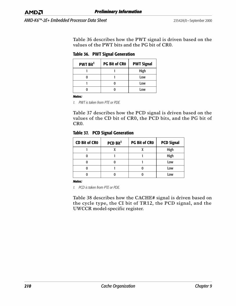
AMD-K6™-2E+ Embedded Processor Data Sheet 23542A/0—September 2000
Preliminary Information
Table 36 describes how the PWT signal is driven based on thevalues of the PWT bits and the PG bit of CR0.
Table 37 describes how the PCD signal is driven based on thevalues of the CD bit of CR0, the PCD bits, and the PG bit ofCR0.
Table 38 describes how the CACHE# signal is driven based onthe cycle type, the CI bit of TR12, the PCD signal, and theUWCCR model-specific register.
Table 36. PWT Signal Generation
PWT Bit1
Notes:
1. PWT is taken from PTE or PDE.
PG Bit of CR0 PWT Signal
1 1 High
0 1 Low
1 0 Low
0 0 Low
Table 37. PCD Signal Generation
CD Bit of CR0 PCD Bit1
Notes:
1. PCD is taken from PTE or PDE.
PG Bit of CR0 PCD Signal
1 X X High
0 1 1 High
0 0 1 Low
0 1 0 Low
0 0 0 Low
210 Cache Organization Chapter 9

23542A/0—September 2000 AMD-K6™-2E+ Embedded Processor Data Sheet
Preliminary Information
Cache-Related Signals Complete descriptions of the signals that control cacheabilityand cache coherency are given on the following pages:
■ CACHE#—page 105
■ EADS#—page 109
■ FLUSH#—page 112
■ HIT#—page 113
■ HITM#—page 113
■ INV—page 118
■ KEN#—page 119
■ PCD—page 124
■ PWT—page 126
■ WB/WT#—page 139
9.4 Cache Disabling and Flushing
L1 and L2 Cache Disabling
To completely disable all accesses to the L1 and the L2 caches,the CD bit must be set to 1 and the caches must be completelyflushed. There are three different methods for flushing thecaches. The first method relies on the system logic and theother two methods rely on software.
■ For the system logic to flush the caches, the processor mustsample FLUSH# asserted. In this method, the processorwrites back any L1 data cache and L2 cache lines that are in
Table 38. CACHE# Signal Generation
Cycle Type CI Bit of TR12 PCD Signal Access Within WC/UC Range1
Notes:
1. WC and UC refer to Write-Combining and Uncacheable Memory Ranges as defined in the UWCCR.
CACHE#
Writebacks X X X Low
Unlocked Reads 0 0 0 Low
Locked Reads X X X High
Single Writes X X X High
Any Cycle Except Writebacks 1 X X High
Any Cycle Except Writebacks X 1 X High
Any Cycle Except Writebacks X X 1 High
Chapter 9 Cache Organization 211
AMD-K6™-2E+ Embedded Processor Data Sheet 23542A/0—September 2000
Preliminary Information
the modified state, invalidates all lines in all caches, andthen executes a flush acknowledge special cycle (SeeTable 24 on page 142).
■ The second method for flushing the caches is for software toexecute the WBINVD instruction, which causes all modifiedlines to first be written back to memory, then marks allcache lines as invalid. Alternatively, if writing modified linesback to memory is not necessary, the INVD instruction canbe used to invalidate all cache lines.
■ The third method for flushing the caches is to make use ofthe Page Flush/Invalidate Register (PFIR), which allowscache invalidation and optional flushing of a specific 4-Kbyte page from the linear address space (see “PageFlush/Invalidate Register (PFIR)” on page 223). Unlike theprevious two methods of flushing the caches, this particularmethod requires the software to be aware of which specificpages must be flushed and invalidated.
L2 Cache Disabling The L2 cache in the AMD-K6-2E+ processor can be completelydisabled by setting the L2 Disable (L2D) bit (EFER[4]) to 1 (see“Extended Feature Enable Register (EFER)” on page 47). Ifdisabled in this manner, the processor does not access the L2cache for any purpose, including allocations, read hits, writehits, snoops, inquire cycles, flushing, and read/write attemptsby means of the L2AAR. (See “L2 Cache Testing” on page 213.)The L1 cache operation is not affected by disabling the L2cache.
The L2D bit is provided for debug and testing purposes only. Fornormal operation and maximum performance, this bit must beset to 0, which is the default setting following reset.
The AMD-K6-2E+ processor does not provide a method fordisabling the L1 cache while the L2 cache remains enabled.
212 Cache Organization Chapter 9
23542A/0—September 2000 AMD-K6™-2E+ Embedded Processor Data Sheet
Preliminary Information
9.5 L2 Cache Testing
The AMD-K6-2E+ processor provides the L2AAR MSR thatallows for direct access to the L2 cache and L2 tag arrays. Formore detailed information, refer to “L2 Cache and Tag ArrayTesting” on page 264.
9.6 Cache-Line Fills
The processor performs a cache-line fill for any area of systemmemory defined as cacheable. If an area of system memory isnot explicitly defined as uncacheable by the software or systemlogic, or implicitly treated as uncacheable by the processor,then the memory access is assumed to be cacheable.
Software can prevent caching of certain pages by setting thePCD bit in the PDE or PTE. Additionally, software can defineregions of memory as uncacheable or write combinable byprogramming the MTRRs in the UWCCR MSR (see “MemoryType Range Registers” on page 231). Write-combinablememory is defined as uncacheable.
The system logic also has control of the cacheability of buscycles. If it determines the address is not cacheable, systemlogic negates the KEN# signal when asserting the first BRDY#or NA# of a cycle.
The processor does not cache certain memory accesses such aslocked operations. In addition, the processor does not cachePDE or PTE memory reads in the L1 cache (referred to as pagetable walks). However, page table walks are cached in the L2cache if the PDE or PTE is determined to be cacheable.
When the processor needs to read memory, the processor drivesa read cycle onto the bus. If the cycle is cacheable, theprocessor asserts CACHE#. If the cycle is not cacheable, anon-burst, single-transfer read takes place. The processor waitsfor the system logic to return the data and assert a singleBRDY# (See Figure 60 on page 159). If the cycle is cacheable,the processor executes a 32-byte burst read cycle. The processorexpects a total of four BRDY# signals for a burst read cycle totake place (See Figure 62 on page 163).
Chapter 9 Cache Organization 213
AMD-K6™-2E+ Embedded Processor Data Sheet 23542A/0—September 2000
Preliminary Information
Cache-line fills initiate 32-byte burst read cycles from memoryon the system bus for the L1 instruction cache and the L1 datacache. All L1 cache-line fills supplied from the system bus arealso filled in the L2 cache.
9.7 Cache-Line Replacements
As programs execute and task switches occur, some cache lineseventually require replacement.
When a cache miss occurs in the L1 cache, the required cacheline is filled from either the L2 cache, if the cache line ispresent (L2 cache hit), or from external memory, if the cacheline is not present (L2 cache miss). If the cache line is filledfrom external memory, the cache line is filled in both the L1and the L2 caches.
Two forms of cache misses and associated cache fills can takeplace—a tag-miss cache fill and a tag-hit cache fill.
■ In the case of a tag-miss cache fill, the level-one cache miss isdue to a tag mismatch, in which case the required cache lineis filled either from the level-two cache or from externalmemory, and the level-one cache line within the sector thatwas not required is marked as invalid.
■ In the case of a tag-hit cache fill, the address matches thetag, but the requested cache line is marked as invalid. Therequired level-one cache line is filled from the level-twocache or from external memory, and the level-one cache linewithin the sector that is not required remains in the samecache state.
If a L1 data-cache line being filled replaces a modified line, themodified line is written back to the L2 cache if the cache line ispresent (L2 cache hit). By design, if a cache line is in themodified state in the L1 cache, this cache line can only exist inthe L2 cache in the exclusive state. During the writeback, theL2 cache-line state is changed from exclusive to modified, andthe writeback does not occur on the system bus. If thereplacement writeback does not hit the L2 cache (L2 cachemiss), then the modified L1 cache line is written back on thesystem bus, and the L2 cache is not updated. If the other cacheline in this sector is in the modified state, it is also written backin the same manner.
214 Cache Organization Chapter 9
23542A/0—September 2000 AMD-K6™-2E+ Embedded Processor Data Sheet
Preliminary Information
L1 instruction-cache lines and L2 cache lines are replaced usinga Least Recently Used (LRU) algorithm. If a line replacement isrequired, lines are replaced when read cache misses occur.
The L1 data cache uses a slightly different approach to linereplacement. If a miss occurs, and a replacement is required,lines are replaced by using a Least Recently Allocated (LRA)algorithm.
9.8 Write Allocate
Write allocate, if enabled, occurs when the processor has apending memory write cycle to a cacheable line and the linedoes not currently reside in the L1 data cache. If the line doesnot exist in the L2 cache, the processor performs a 32-byte burstread cycle on the system bus to fetch the data-cache lineaddressed by the pending write cycle. If the line does exist inthe L2 cache, the data is supplied directly from the L2 cache, inwhich case a system bus cycle is not executed. The dataassociated with the pending write cycle is merged with therecently-allocated data-cache line and stored in the processor’sL1 data cache. If the data-cache line was fetched from memory(because of a L2 cache miss), the data is stored, withoutmodification, in the L2 cache. The final MESI state of the cachelines depends on the state of the WB/WT# and PWT signalsduring the burst read cycle and the subsequent L1 data cachewrite hit (See Table 39 on page 221 to determine the cache-linestates and the access types following a cache write miss). If theL1 data cache line is stored in the modified state, then the samecache line is stored in the L2 cache in the exclusive state. If theL1 data cache line is stored in the shared state, then the samecache line is stored in the L2 cache in the shared state.
If a data-cache line fetch from memory is attempted becausethe write allocate misses the L2 cache, and KEN# is samplednegated, the processor does not perform an allocation. In thiscase, the pending write cycle is executed as a single write cycleon the system bus.
During write allocates that miss the L2 cache, a 32-byte burstread cycle is executed in place of a non-burst write cycle. Whilethe burst read cycle generally takes longer to execute than thenon-burst write cycle, performance gains are realized onsubsequent write cycle hits to the write-allocated cache line.
Chapter 9 Cache Organization 215
AMD-K6™-2E+ Embedded Processor Data Sheet 23542A/0—September 2000
Preliminary Information
Due to the nature of software, memory accesses tend to occur inproximity of each other (principle of locality). The likelihood ofadditional write hits to the write-allocated cache line is high.
Write allocates that hit the L2 cache increase performance byavoiding accesses to the system bus.
The following is a description of three mechanisms by which theAMD-K6-2E+ processor performs write allocations. A writeallocate is performed when any one or more of thesemechanisms indicates that a pending write is to a cacheablearea of memory.
Write to a Cacheable Page
Every time the processor completes a L1 cache line fill, theaddress of the page in which the cache line resides is saved inthe Cacheability Control Register (CCR). The page address ofsubsequent write cycles is compared with the page addressstored in the CCR. If the two addresses are equal, then theprocessor performs a write allocate because the page hasalready been determined to be cacheable.
When the processor performs a L1 cache line fill from adifferent page than the address saved in the CCR, the CCR isupdated with the new page address.
Write to a Sector If the address of a pending write cycle matches the tag addressof a valid L1 cache sector, but the addressed cache line withinthe sector is marked invalid (a sector hit but a cache line miss),then the processor performs a write allocate. The pending writecycle is determined to be cacheable because the sector hitindicates the presence of at least one valid cache line in thesector. The two cache lines within a sector are guaranteed bydesign to be within the same page.
Write Allocate Limit The AMD-K6-2E+ processor uses two mechanisms that areprogrammable within the Write Handling Control Register(WHCR) to enable write allocations for write cycles thataddress a definable area, or a special 1-Mbyte memory area.
The WHCR contains two fields—the Write Allocate EnableLimit (WAELIM) field, and the Write Allocate Enable15-to-16-Mbyte (WAE15M) bit (see Figure 84).
216 Cache Organization Chapter 9
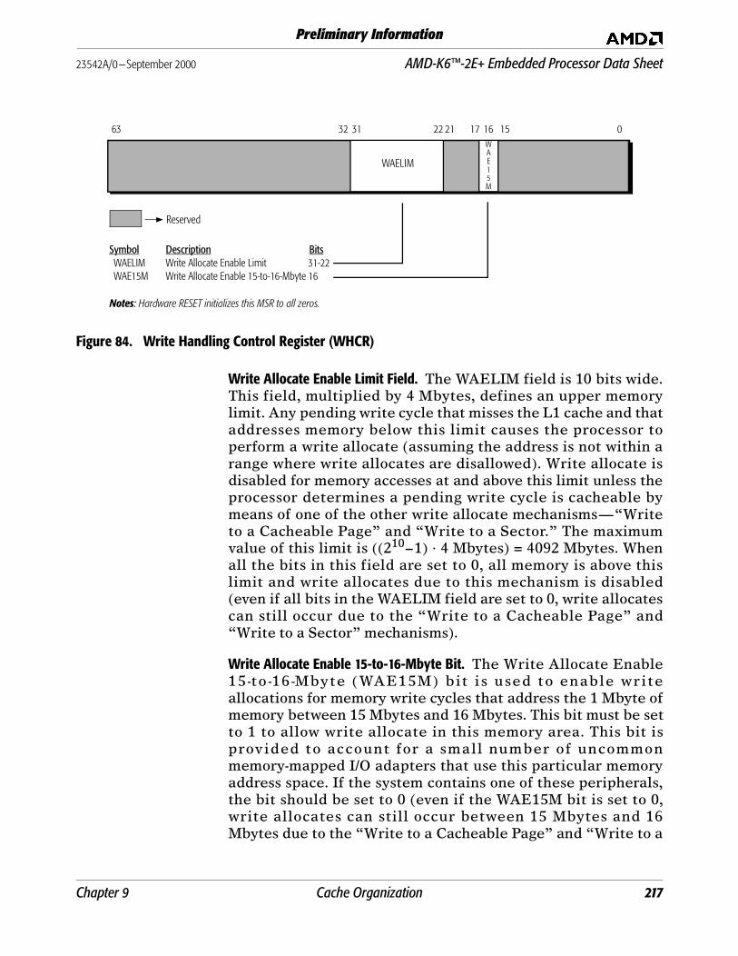
23542A/0—September 2000 AMD-K6™-2E+ Embedded Processor Data Sheet
Preliminary Information
Figure 84. Write Handling Control Register (WHCR)
Write Allocate Enable Limit Field. The WAELIM field is 10 bits wide.This field, multiplied by 4 Mbytes, defines an upper memorylimit. Any pending write cycle that misses the L1 cache and thataddresses memory below this limit causes the processor toperform a write allocate (assuming the address is not within arange where write allocates are disallowed). Write allocate isdisabled for memory accesses at and above this limit unless theprocessor determines a pending write cycle is cacheable bymeans of one of the other write allocate mechanisms—“Writeto a Cacheable Page” and “Write to a Sector.” The maximumvalue of this limit is ((210–1) · 4 Mbytes) = 4092 Mbytes. Whenall the bits in this field are set to 0, all memory is above thislimit and write allocates due to this mechanism is disabled(even if all bits in the WAELIM field are set to 0, write allocatescan still occur due to the “Write to a Cacheable Page” and“Write to a Sector” mechanisms).
Write Allocate Enable 15-to-16-Mbyte Bit. The Write Allocate Enable15-to-16-Mbyte (WAE15M) bit is used to enable writeallocations for memory write cycles that address the 1 Mbyte ofmemory between 15 Mbytes and 16 Mbytes. This bit must be setto 1 to allow write allocate in this memory area. This bit isprovided to account for a small number of uncommonmemory-mapped I/O adapters that use this particular memoryaddress space. If the system contains one of these peripherals,the bit should be set to 0 (even if the WAE15M bit is set to 0,write allocates can still occur between 15 Mbytes and 16Mbytes due to the “Write to a Cacheable Page” and “Write to a
1522 063
Reserved
WAELIM
16
Notes: Hardware RESET initializes this MSR to all zeros.
WAE15M
Symbol Description BitsWAELIM Write Allocate Enable Limit 31-22WAE15M Write Allocate Enable 15-to-16-Mbyte 16
17213132
Chapter 9 Cache Organization 217
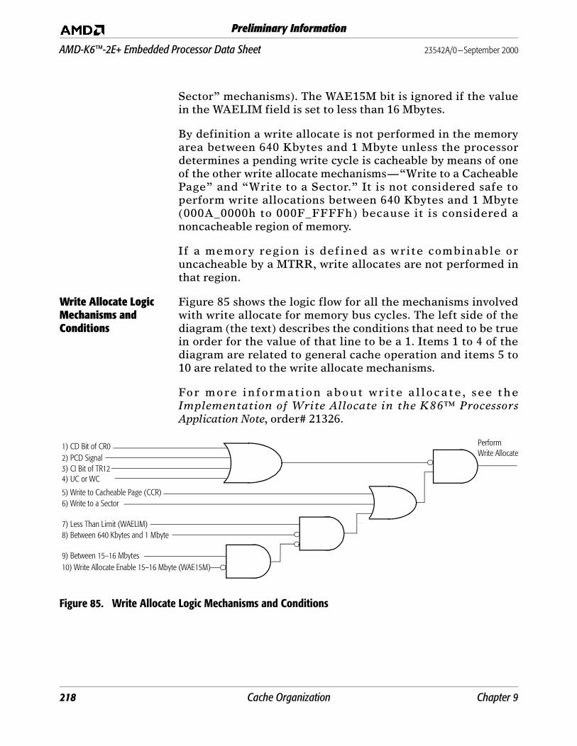
AMD-K6™-2E+ Embedded Processor Data Sheet 23542A/0—September 2000
Preliminary Information
Sector” mechanisms). The WAE15M bit is ignored if the valuein the WAELIM field is set to less than 16 Mbytes.
By definition a write allocate is not performed in the memoryarea between 640 Kbytes and 1 Mbyte unless the processordetermines a pending write cycle is cacheable by means of oneof the other write allocate mechanisms—“Write to a CacheablePage” and “Write to a Sector.” It is not considered safe toperform write allocations between 640 Kbytes and 1 Mbyte(000A_0000h to 000F_FFFFh) because it is considered anoncacheable region of memory.
If a memory region is defined as write combinable oruncacheable by a MTRR, write allocates are not performed inthat region.
Write Allocate Logic Mechanisms and Conditions
Figure 85 shows the logic flow for all the mechanisms involvedwith write allocate for memory bus cycles. The left side of thediagram (the text) describes the conditions that need to be truein order for the value of that line to be a 1. Items 1 to 4 of thediagram are related to general cache operation and items 5 to10 are related to the write allocate mechanisms.
For more informat ion about write a l locate , see theImplementation of Write Allocate in the K86™ ProcessorsApplication Note, order# 21326.
Figure 85. Write Allocate Logic Mechanisms and Conditions
1) CD Bit of CR0 PerformWrite Allocate
3) CI Bit of TR122) PCD Signal
5) Write to Cacheable Page (CCR)6) Write to a Sector
8) Between 640 Kbytes and 1 Mbyte7) Less Than Limit (WAELIM)
9) Between 15–16 Mbytes10) Write Allocate Enable 15–16 Mbyte (WAE15M)
4) UC or WC
218 Cache Organization Chapter 9
23542A/0—September 2000 AMD-K6™-2E+ Embedded Processor Data Sheet
Preliminary Information
The following list describes the corresponding items in Figure85:
1. CD Bit of CR0—When the cache disable (CD) bit within con-trol register 0 (CR0) is set to 1, the cache fill mechanism for both reads and writes is disabled and write allocate does not occur.
2. PCD Signal—When the PCD (page cache disable) signal isdriven High, caching for that page is disabled, even if KEN#is sampled asserted, and write allocate does not occur.
3. CI Bit of TR12—When the cache inhibit bit of Test Register12 is set to 1, L1 and L2 cache fills are disabled and writeallocate does not occur.
4. UC or WC—If a pending write cycle addresses a region ofmemory defined as write combinable or uncacheable by anMTRR, write allocates are not performed in that region.
5. Write to a Cacheable Page (CCR)—A write allocate isperformed if the processor knows that a page is cacheable.The CCR is used to store the page address of the last L1cache fill for a read miss. See “Write to a Cacheable Page”on page 216 for a detailed description of this condition.
6. Write to a Sector—A write allocate is performed if theaddress of a pending write cycle matches the tag address ofa valid L1 cache sector but the addressed cache line withinthe sector is invalid. See “Write to a Sector” on page 216 fora detailed description of this condition.
7. Less Than Limit (WAELIM)—The write allocate limitmechanism determines if the memory area being addressedis less than the limit set in the WAELIM field of WHCR. Ifthe address is less than the limit, write allocate for thatmemory address is performed as long as conditions 8through 10 do not prevent write allocate (even if conditions8 and 10 attempt to prevent write allocate, condition 5 or 6allows write allocate to occur).
8. Between 640 Kbytes and 1 Mbyte—Write allocate is notperformed in the memory area between 640 Kbytes and 1Mbyte. It is not considered safe to perform write allocationsbetween 640 Kbytes and 1 Mbyte (000A_0000h to000F_FFFFh) because this area of memory is considered anoncacheable region of memory (even if condition 8attempts to prevent write allocate, condition 5 or 6 allowswrite allocate to occur).
Chapter 9 Cache Organization 219
AMD-K6™-2E+ Embedded Processor Data Sheet 23542A/0—September 2000
Preliminary Information
9. Between 15–16 Mbytes—If the address of a pending writecycle is in the 1 Mbyte of memory between 15 Mbytes and16 Mbytes, and the WAE15M bit is set to 1, write allocatefor this cycle is enabled.
10.Write Allocate Enable 15–16 Mbytes (WAE15M)—Thiscondition is associated with the Write Allocate Limitmechanism and affects write allocate only if the limitspecified by the WAELIM field is greater than or equal to16 Mbytes. If the memory address is between 15 Mbytes and16 Mbytes, and the WAE15M bit in the WHCR is set to 0,write allocate for this cycle is disabled (even if condition 10attempts to prevent write allocate, condition 5 or 6 allowswrite allocate to occur).
9.9 Prefetching
Hardware Prefetching
The AMD-K6-2E+ processor conditionally performs cacheprefetching, which results in the filling of the required cacheline first, and a prefetch of the second cache line making up theother half of the sector. From the perspective of the externalbus, the two cache-line fills typically appear as two 32-byteburst read cycles occurring back-to-back or, if allowed, aspipelined cycles. The burst read cycles do not occurback-to-back (wait states occur) if the processor is not ready tostart a new cycle, if higher priority data read or write requestsexist, or if NA# (next address) was sampled negated. Wait statescan also exist between burst cycles if the processor samplesAHOLD or BOFF# asserted.
Software Prefetching The 3DNow! technology includes an instruction calledPREFETCH that allows a cache line to be prefetched into theL1 data cache and the L2 cache. Unlike prefetching underhardware control, software prefetching only fetches the cacheline specified by the operand of the PREFETCH instruction,and does not attempt to fetch the other cache line in the sector.The PREFETCH instruction format is defined in Table 15,“3DNow!™ Instructions,” on page 89. For more detailedinformation, see the 3DNow!™ Technology Manual, order#21928.
220 Cache Organization Chapter 9

23542A/0—September 2000 AMD-K6™-2E+ Embedded Processor Data Sheet
Preliminary Information
9.10 Cache States
Table 39 shows all the possible cache-line states before andafter program-generated accesses to individual cache lines.
Table 39. L1 and L2 Cache States for Read and Write Accesses
TypeCache State Before Access1
Access Type
Cache State After Access
MESI State2
L1 L2 L1 L2
Cache Read
Read Miss L1, Read Miss L2
I I Single read from bus I I
I I Burst read from bus, fill L1 and L23 S or E4 S or E4
Read Hit L1E – – E –S – – S –M – – M –
Read Miss L1, Read Hit L2
I E Fill L1 E EI S Fill L1 S SI M Fill L1 M E
I M Fill L1 E5 M5
Cache Write
Write Miss L1
Write Miss L2
I I Single write to bus6 I I
I I Burst read from bus, fill L1 and L2, write to L17 M8 E8
I IBurst read from bus, fill L1 and L2, write to L1 and L2, single write to bus7 S9 S9
Write Hit L1
S IWrite to L1, single write to bus S or E4 I
S SWrite to L1 and L2, single write to bus S or E4 S or E4
E or M – Write to L1 M –
Write Miss L1
Write Hit L2
I E Write to L26 I M
I S Write to L2, single write to bus6 I S or E4
I M Write to L26 I M
I E Fill L1, write to L17 M E
I S Write to L2, single write to bus7 S or E4 S or E4
I M Fill L1, write to L17 M E
Notes:
1. M = Modified, E = Exclusive, S = Shared, I = Invalid. The exclusive and shared states are indistinguishable in the L1 instruction cache and are treated as “valid” states.
2. The final MESI state assumes that the state of the WB/WT# signal remains the same for all accesses to a particular cache line.3. If CACHE# is driven Low and KEN# is sampled asserted.4. If PWT is driven Low and WB/WT# is sampled High, the line is cached in the exclusive (writeback) state. If PWT is driven High or
WB/WT# is sampled Low, the line is cached in the shared (writethrough) state.
Chapter 9 Cache Organization 221

AMD-K6™-2E+ Embedded Processor Data Sheet 23542A/0—September 2000
Preliminary Information
9.11 Cache Coherency
Different ways exist to maintain coherency between the systemmemory and cache memories. Inquire cycles, internal snoops,FLUSH#, WBINVD, INVD, and line replacements all preventinconsistencies between memories.
Inquire Cycles Inquire cycles are bus cycles initiated by system logic thatensure coherency between the caches and main memory. Insystems with multiple bus masters, system logic maintainscache coherency by driving inquire cycles to the processor.System logic initiates inquire cycles by asserting AHOLD,BOFF#, or HOLD to obtain control of the address bus and thendriving EADS#, INV (optional), and an inquire address(A[31:5]).
This type of bus cycle causes the processor to compare the tagsfor its L1 instruction and L1 data caches, and L2 cache, with theinquire address.
■ If there is a hit to a shared or exclusive line in the L1 datacache or the L2 cache, or a valid line in the L1 instructioncache, the processor asserts HIT#.
■ If the compare hits a modified line in the L1 data cache orthe L2 cache, the processor asserts HIT# and HITM#. IfHITM# is asserted, the processor writes the modified lineback to memory.
■ If INV was sampled asserted with EADS#, a hit invalidatesthe line.
■ If INV was sampled negated with EADS#, a hit leaves theline in the shared state or transitions it from the exclusive ormodified state to the shared state.
Table 40 on page 225 lists valid combinations of MESI statespermitted for a cache line in the L1 and L2 caches, and showsthe effects of inquire cycles performed with INV equal to 0(non-invalidating) and INV equal to 1 (invalidating).
5. This entry only applies to the L1 instruction cache. By design, a cache line cannot exist in the exclusive state in the L1 data cache and in the modified state in the L2 cache.
6. Assumes the write allocate conditions as specified in “Write Allocate” on page 215 are not met.7. Assumes the write allocate conditions as specified in “Write Allocate” on page 215 are met.8. Assumes PWT is driven Low and WB/WT# is sampled High.9. Assumes PWT is driven High or WB/WT# is sampled Low.— Not applicable or none.
222 Cache Organization Chapter 9
23542A/0—September 2000 AMD-K6™-2E+ Embedded Processor Data Sheet
Preliminary Information
Internal Snooping Internal snooping is initiated by the processor (rather thansystem logic) during certain cache accesses. It is used tomaintain coherency between the L1 instruction cache and theL1 data cache.
The processor automatically snoops its L1 instruction cacheduring read or write misses to its L1 data cache, and it snoopsits L1 data cache during read misses to its L1 instruction cache.The L2 cache is not snooped during misses to either of the L1caches. Table 41 on page 226 summarizes the actions takenduring this internal snooping.
If an internal snoop hits its target, the processor does thefollowing:
■ L1 Data Cache Snoop During an L1 Instruction-cache ReadMiss—If modified, the line in the L1 data cache is writtenback. If the writeback hits the L2 cache, the cache line isstored in the L2 cache in the modified state and nowriteback occurs on the system bus. If the writeback missesthe L2 cache, the cache line is written back on the systembus to external memory. Regardless of its state, the L1data-cache line is invalidated and the L1 instruction cacheperforms a read from either the L2 cache (if a L2 hit occurs)or external memory (if a L2 miss occurs).
■ L1 Instruction Cache Snoop During an L1 Data CacheMiss—The line in the instruction cache is marked invalid,and the L1 data-cache read or write is performed as definedin Table 39 on page 221.
FLUSH# In response to sampling FLUSH# asserted, the processor writesback any L1 data cache lines and L2 cache lines that are in themodified state and then marks all lines in the L1 instructioncache, the L1 data cache, and the L2 cache as invalid.
Page Flush/Invalidate Register (PFIR)
The AMD-K6-2E+ processor contains the Page Flush/InvalidateRegister (PFIR) that allows cache invalidation and optionalflushing of a specific 4-Kbyte page from the linear addressspace (see Figure 86 on page 224). When the PFIR is written to(using the WRMSR instruction), the invalidation and,optionally, the flushing begins. The total amount of cache in theAMD-K6-2E+ processor is 128 Kbytes. Using this register canresult in a much lower cycle count for flushing particular pagesversus flushing the entire cache.
Chapter 9 Cache Organization 223
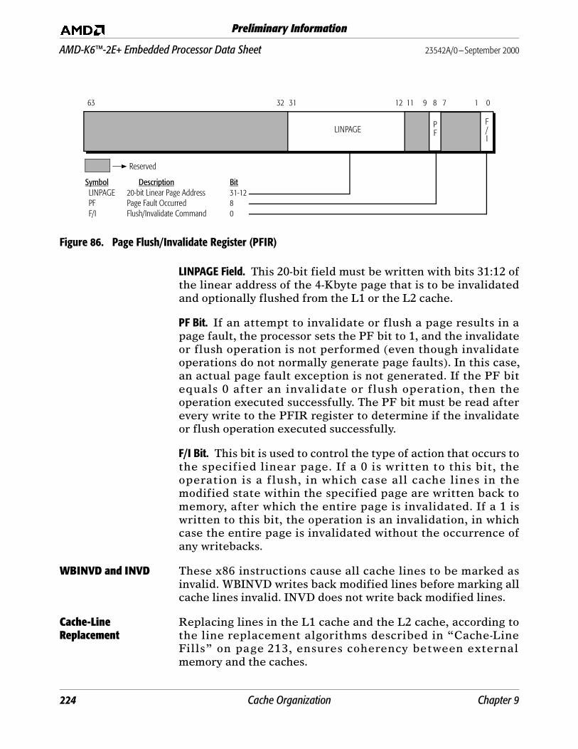
AMD-K6™-2E+ Embedded Processor Data Sheet 23542A/0—September 2000
Preliminary Information
Figure 86. Page Flush/Invalidate Register (PFIR)
LINPAGE Field. This 20-bit field must be written with bits 31:12 ofthe linear address of the 4-Kbyte page that is to be invalidatedand optionally flushed from the L1 or the L2 cache.
PF Bit. If an attempt to invalidate or flush a page results in apage fault, the processor sets the PF bit to 1, and the invalidateor flush operation is not performed (even though invalidateoperations do not normally generate page faults). In this case,an actual page fault exception is not generated. If the PF bitequals 0 after an invalidate or flush operation, then theoperation executed successfully. The PF bit must be read afterevery write to the PFIR register to determine if the invalidateor flush operation executed successfully.
F/I Bit. This bit is used to control the type of action that occurs tothe specified linear page. If a 0 is written to this bit, theoperation is a flush, in which case all cache lines in themodified state within the specified page are written back tomemory, after which the entire page is invalidated. If a 1 iswritten to this bit, the operation is an invalidation, in whichcase the entire page is invalidated without the occurrence ofany writebacks.
WBINVD and INVD These x86 instructions cause all cache lines to be marked asinvalid. WBINVD writes back modified lines before marking allcache lines invalid. INVD does not write back modified lines.
Cache-Line Replacement
Replacing lines in the L1 cache and the L2 cache, according tothe line replacement algorithms described in “Cache-LineFills” on page 213, ensures coherency between externalmemory and the caches.
LINPAGE
1 063
F/I
Reserved
Symbol Description BitLINPAGE 20-bit Linear Page Address 31-12PF Page Fault Occurred 8F/I Flush/Invalidate Command 0
1131 1232
PF
9 8 7
224 Cache Organization Chapter 9

23542A/0—September 2000 AMD-K6™-2E+ Embedded Processor Data Sheet
Preliminary Information
Table 40 shows all possible cache-line states before and afterinquire cycles.
Table 40. Valid L1 and L2 Cache States and Effect of Inquire Cycles
Cache State Before Inquire1
Notes:
1. M = Modified, E = Exclusive, S = Shared, I = Invalid. The exclusive and shared states are indistinguishable in the L1 instruction cache and are treated as “valid” states.
Memory Access2
2. Writeback cycles to the bus are 32-byte burst writes.
Cache State After Inquire
INV = 0 INV = 1
L1 L2 L1 L2 L1 L2I M Writeback L2 to bus I S I I
I E – I S I I
I S – I S I I
I I – I I I I
E3
3. This entry only applies to the L1 instruction cache. By design, a cache line cannot exist in the exclusive state in the L1 data cache and in the modified state in the L2 cache.
M3 Writeback L2 to bus S S I I
E E – S S I I
E I – S I I I
M E Writeback L1 to bus S I I I
M I Writeback L1 to bus S I I I
S S – S S I I
S I – S I I I
Chapter 9 Cache Organization 225
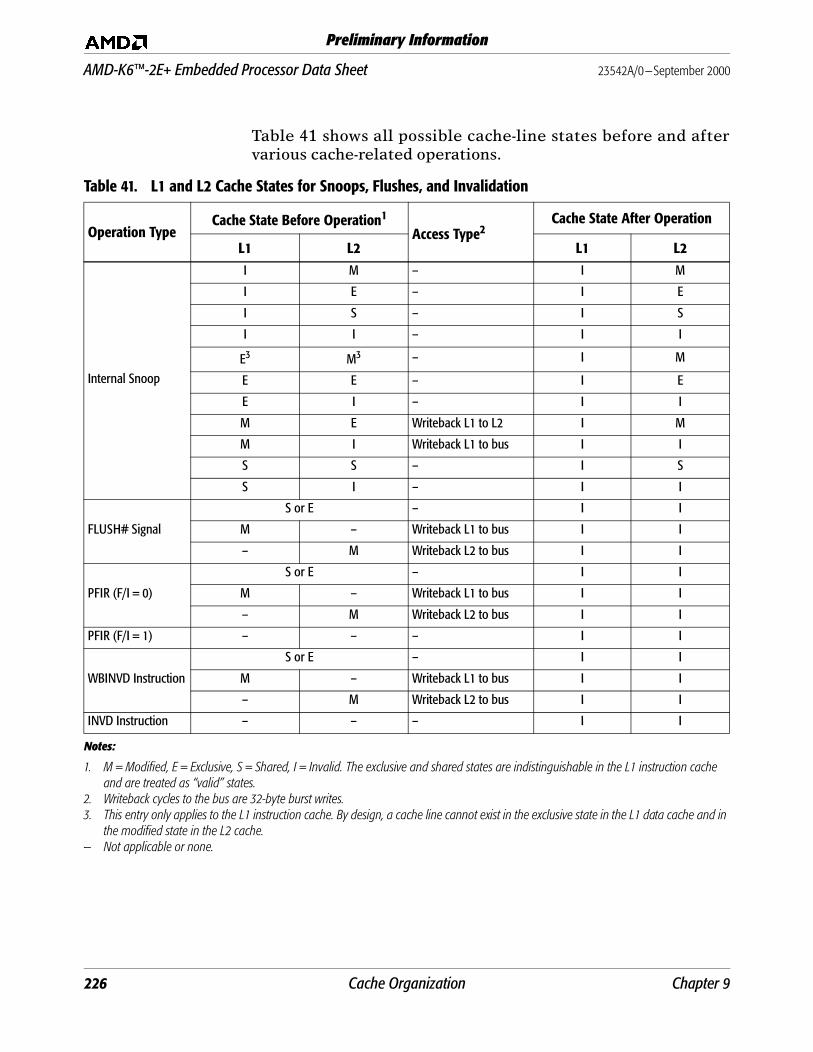
AMD-K6™-2E+ Embedded Processor Data Sheet 23542A/0—September 2000
Preliminary Information
Table 41 shows all possible cache-line states before and aftervarious cache-related operations.
Table 41. L1 and L2 Cache States for Snoops, Flushes, and Invalidation
Operation TypeCache State Before Operation1
Notes:
1. M = Modified, E = Exclusive, S = Shared, I = Invalid. The exclusive and shared states are indistinguishable in the L1 instruction cache and are treated as “valid” states.
Access Type2
2. Writeback cycles to the bus are 32-byte burst writes.
Cache State After Operation
L1 L2 L1 L2
Internal Snoop
I M – I M
I E – I E
I S – I S
I I – I I
E3
3. This entry only applies to the L1 instruction cache. By design, a cache line cannot exist in the exclusive state in the L1 data cache and in the modified state in the L2 cache.
— Not applicable or none.
M3 – I M
E E – I E
E I – I I
M E Writeback L1 to L2 I M
M I Writeback L1 to bus I I
S S – I S
S I – I I
FLUSH# Signal
S or E – I I
M – Writeback L1 to bus I I
– M Writeback L2 to bus I I
PFIR (F/I = 0)
S or E – I I
M – Writeback L1 to bus I I
– M Writeback L2 to bus I I
PFIR (F/I = 1) – – – I I
WBINVD Instruction
S or E – I I
M – Writeback L1 to bus I I
– M Writeback L2 to bus I I
INVD Instruction – – – I I
226 Cache Organization Chapter 9
23542A/0—September 2000 AMD-K6™-2E+ Embedded Processor Data Sheet
Preliminary Information
9.12 Writethrough and Writeback Coherency States
The terms writethrough and writeback apply to two relatedconcepts in a read-write cache like the AMD-K6-2E+ processorL1 data cache and the L2 cache. The following conditions applyto both the writethrough and writeback modes:
■ Memory Writes—A relationship exists between externalmemory writes and their concurrence with cache updates:
• An external memory write that occurs concurrently witha cache update to the same location is a writethrough.Writethroughs are driven as single cycles on the bus.
• An external memory write that occurs after the processorhas modified a cache line is a writeback. Writebacks aredriven as burst cycles on the bus.
■ Coherency State—A relationship exists between MESIcoherency states and writethrough-writeback coherencystates of lines in the cache as follows:
• Shared and invalid MESI lines are in the writethroughstate.
• Modified and exclusive MESI lines are in the writebackstate.
9.13 A20M# Masking of Cache Accesses
Although the processor samples A20M# as a level-sensitiveinput on every clock edge, it should only be asserted in Realmode. The processor applies the A20M# masking to its tags,through which all programs access the caches. Therefore,assertion of A20M# affects all addresses (cache and externalmemory), including the following:
■ Cache-line fills (caused by read misses or write allocates)
■ Cache writethroughs (caused by write misses or write hits tolines in the shared state)
However, A20M# does not mask writebacks or invalidationscaused by the following actions:
■ Internal snoops
■ Inquire cycles
■ The FLUSH# signal
Chapter 9 Cache Organization 227
AMD-K6™-2E+ Embedded Processor Data Sheet 23542A/0—September 2000
Preliminary Information
■ Writing to the Page Flush/Invalidate Register (PFIR)
■ The WBINVD instruction
228 Cache Organization Chapter 9
23542A/0—September 2000 AMD-K6™-2E+ Embedded Processor Data Sheet
Preliminary Information
10 Write Merge Buffer
The AMD-K6-2E+ processor contains an 8-byte write mergebuffer that allows the processor to conditionally combine datafrom multiple noncacheable write cycles into this merge buffer.The merge buffer operates in conjunction with the MemoryType Range Registers (MTRRs). Refer to “Memory Type RangeRegisters” on page 231 for a description of the MTRRs.
Merging multiple write cycles into a single write cycle reducesprocessor bus utilization and processor stalls, therebyincreasing the overall system performance.
10.1 EWBE# Control
The presence of the merge buffer creates the potential toperform out-of-order write cycles relative to the processor’scaches. In general, the ordering of write cycles that are drivenexternally on the system bus and those that hit the processor’scache can be controlled by the EWBE# signal. See “EWBE#(External Write Buffer Empty)” on page 110 for moreinformation.
If EWBE# is sampled negated, the processor delays thecommitment of write cycles to cache lines in the modified stateor exclusive state in the processor’s caches. Therefore, thesystem logic can enforce strong ordering by negating EWBE#until the external write cycle is complete, thereby ensuring thata subsequent write cycle that hits a cache does not completeahead of the external write cycle.
However, the addition of the write merge buffer introduces thepotential for out-of-order write cycles to occur between writesto the merge buffer and writes to the processor’s caches.Because these writes occur entirely within the processor andare not sent out to the processor bus, the system logic is not ableto enforce strong ordering with the EWBE# signal.
The EWBE# control (EWBEC) bits in the EFER register providea mechanism for enforcing three different levels of writeordering in the presence of the write merge buffer:
Chapter 10 Write Merge Buffer 229
AMD-K6™-2E+ Embedded Processor Data Sheet 23542A/0—September 2000
Preliminary Information
■ EFER[3] is defined as the Global EWBE# Disable(GEWBED). When GEWBED equals 1, the processor doesnot attempt to enforce any write ordering internally orexternally (the EWBE# signal is ignored). This is themaximum performance setting.
■ EFER[2] is defined as the Speculative EWBE# Disable(SEWBED). SEWBED only affects the processor whenGEWBED equals 0. If GEWBED equals 0 and SEWBEDequals 1, the processor enforces strong ordering for allinternal write cycles with the exception of write cyclesaddressed to a range of memory defined as uncacheable(UC) or write-combining (WC) by the MTRRs. In addition,the processor samples the EWBE# signal. If EWBE# issampled negated, the processor delays the commitment ofwrite cycles to processor cache lines in the modified state orexclusive state until EWBE# is sampled asserted.
This setting provides performance comparable to, butslightly less than, the performance obtained whenGEWBED equals 1 because some degree of write ordering ismaintained.
■ If GEWBED equals 0 and SEWBED equals 0, the processorenforces strong ordering for all internal and external writecycles. In this setting, the processor assumes, or speculates,that strong order must be maintained between writes to themerge buffer and writes that hit the processor’s caches.Once the merge buffer is written out to the processor’s bus,the EWBE# signal is sampled. If EWBE# is sampled negated,the processor delays the commitment of write cycles toprocessor cache lines in the modified state or exclusive stateuntil EWBE# is sampled asserted.
This setting is the default after RESET and provides thelowest performance of the three settings because full writeordering is maintained.
230 Write Merge Buffer Chapter 10
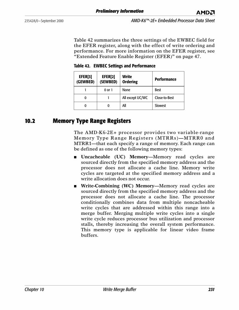
23542A/0—September 2000 AMD-K6™-2E+ Embedded Processor Data Sheet
Preliminary Information
Table 42 summarizes the three settings of the EWBEC field forthe EFER register, along with the effect of write ordering andperformance. For more information on the EFER register, see“Extended Feature Enable Register (EFER)” on page 47.
10.2 Memory Type Range Registers
The AMD-K6-2E+ processor provides two variable-rangeMemory Type Range Registers (MTRRs)—MTRR0 andMTRR1—that each specify a range of memory. Each range canbe defined as one of the following memory types:
■ Uncacheable (UC) Memory—Memory read cycles aresourced directly from the specified memory address and theprocessor does not allocate a cache line. Memory writecycles are targeted at the specified memory address and awrite allocation does not occur.
■ Write-Combining (WC) Memory—Memory read cycles aresourced directly from the specified memory address and theprocessor does not allocate a cache line. The processorconditionally combines data from multiple noncacheablewrite cycles that are addressed within this range into amerge buffer. Merging multiple write cycles into a singlewrite cycle reduces processor bus utilization and processorstalls, thereby increasing the overall system performance.This memory type is applicable for linear video framebuffers.
Table 42. EWBEC Settings and Performance
EFER[3](GEWBED)
EFER[2](SEWBED)
WriteOrdering Performance
1 0 or 1 None Best
0 1 All except UC/WC Close-to-Best
0 0 All Slowest
Chapter 10 Write Merge Buffer 231
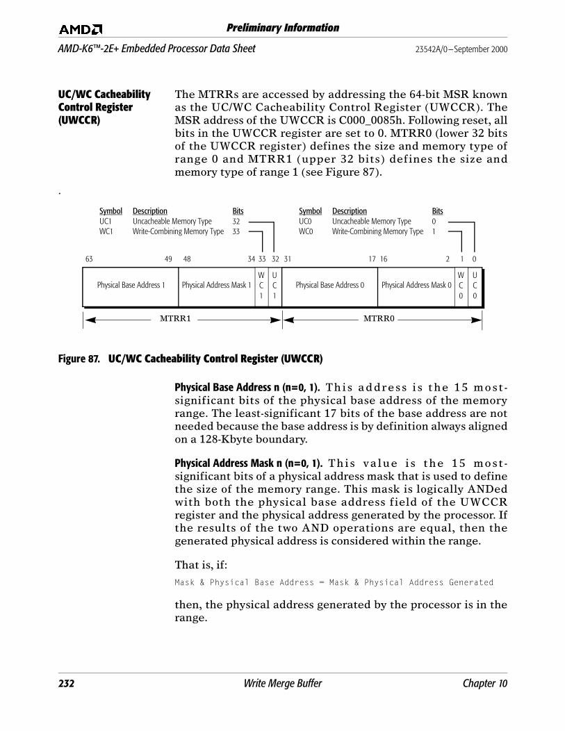
AMD-K6™-2E+ Embedded Processor Data Sheet 23542A/0—September 2000
Preliminary Information
UC/WC Cacheability Control Register(UWCCR)
The MTRRs are accessed by addressing the 64-bit MSR knownas the UC/WC Cacheability Control Register (UWCCR). TheMSR address of the UWCCR is C000_0085h. Following reset, allbits in the UWCCR register are set to 0. MTRR0 (lower 32 bitsof the UWCCR register) defines the size and memory type ofrange 0 and MTRR1 (upper 32 bits) defines the size andmemory type of range 1 (see Figure 87).
.
Figure 87. UC/WC Cacheability Control Register (UWCCR)
Physical Base Address n (n=0, 1). This address is the 15 most -significant bits of the physical base address of the memoryrange. The least-significant 17 bits of the base address are notneeded because the base address is by definition always alignedon a 128-Kbyte boundary.
Physical Address Mask n (n=0, 1). This value i s the 15 most -significant bits of a physical address mask that is used to definethe size of the memory range. This mask is logically ANDedwith both the physical base address field of the UWCCRregister and the physical address generated by the processor. Ifthe results of the two AND operations are equal, then thegenerated physical address is considered within the range.
That is, if:
Mask & Physical Base Address = Mask & Physical Address Generated
then, the physical address generated by the processor is in therange.
16 063
Physical Address Mask 0
1731
Physical Base Address 0
12
Physical Address Mask 1Physical Base Address 1
3233344849
UC0
WC0
UC1
WC1
MTRR1 MTRR0
Symbol Description BitsUC0 Uncacheable Memory Type 0WC0 Write-Combining Memory Type 1
Symbol Description BitsUC1 Uncacheable Memory Type 32WC1 Write-Combining Memory Type 33
232 Write Merge Buffer Chapter 10
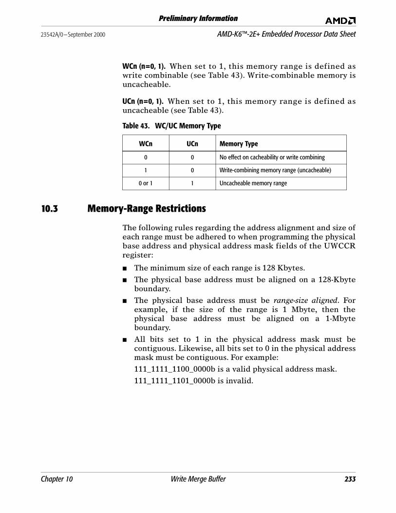
23542A/0—September 2000 AMD-K6™-2E+ Embedded Processor Data Sheet
Preliminary Information
WCn (n=0, 1). When set to 1, this memory range is defined aswrite combinable (see Table 43). Write-combinable memory isuncacheable.
UCn (n=0, 1). When set to 1, this memory range is defined asuncacheable (see Table 43).
10.3 Memory-Range Restrictions
The following rules regarding the address alignment and size ofeach range must be adhered to when programming the physicalbase address and physical address mask fields of the UWCCRregister:
■ The minimum size of each range is 128 Kbytes.
■ The physical base address must be aligned on a 128-Kbyteboundary.
■ The physical base address must be range-size aligned. Forexample, if the size of the range is 1 Mbyte, then thephysical base address must be aligned on a 1-Mbyteboundary.
■ All bits set to 1 in the physical address mask must becontiguous. Likewise, all bits set to 0 in the physical addressmask must be contiguous. For example:
111_1111_1100_0000b is a valid physical address mask.
111_1111_1101_0000b is invalid.
Table 43. WC/UC Memory Type
WCn UCn Memory Type
0 0 No effect on cacheability or write combining
1 0 Write-combining memory range (uncacheable)
0 or 1 1 Uncacheable memory range
Chapter 10 Write Merge Buffer 233
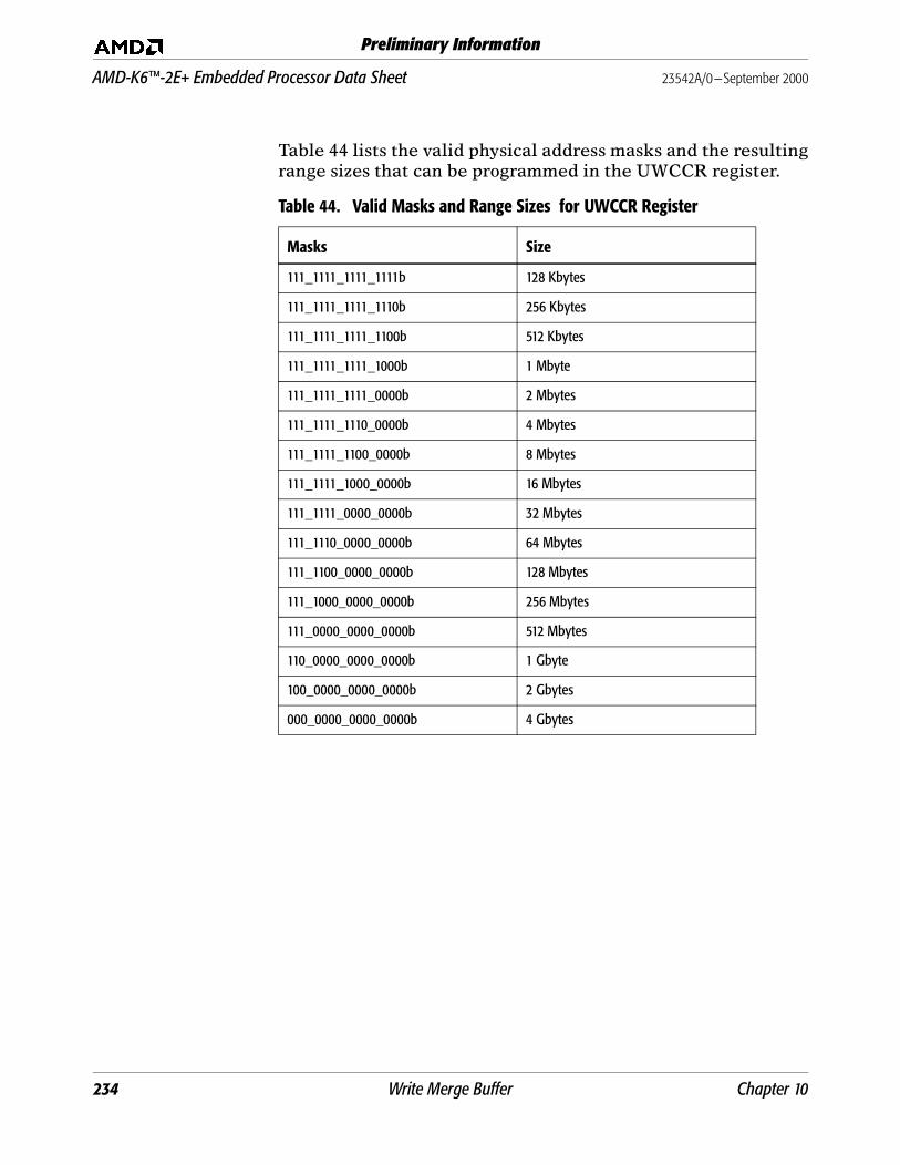
AMD-K6™-2E+ Embedded Processor Data Sheet 23542A/0—September 2000
Preliminary Information
Table 44 lists the valid physical address masks and the resultingrange sizes that can be programmed in the UWCCR register.
Table 44. Valid Masks and Range Sizes for UWCCR Register
Masks Size
111_1111_1111_1111b 128 Kbytes
111_1111_1111_1110b 256 Kbytes
111_1111_1111_1100b 512 Kbytes
111_1111_1111_1000b 1 Mbyte
111_1111_1111_0000b 2 Mbytes
111_1111_1110_0000b 4 Mbytes
111_1111_1100_0000b 8 Mbytes
111_1111_1000_0000b 16 Mbytes
111_1111_0000_0000b 32 Mbytes
111_1110_0000_0000b 64 Mbytes
111_1100_0000_0000b 128 Mbytes
111_1000_0000_0000b 256 Mbytes
111_0000_0000_0000b 512 Mbytes
110_0000_0000_0000b 1 Gbyte
100_0000_0000_0000b 2 Gbytes
000_0000_0000_0000b 4 Gbytes
234 Write Merge Buffer Chapter 10
23542A/0—September 2000 AMD-K6™-2E+ Embedded Processor Data Sheet
Preliminary Information
10.4 Examples
Suppose that the range of memory from 16 Mbytes to 32 Mbytesis uncacheable, and the 8-Mbyte range of memory on top of 1Gbyte is write-combinable. Range 0 is defined as theuncacheable range, and range 1 is defined as the write-combining range.
■ Extracting the 15 most-significant bits of the 32-bit physicalbase address that corresponds to 16 Mbytes (0100_0000h)yields a physical base address 0 field of000_0000_1000_0000b. Because the uncacheable range sizeis 16 Mbytes, the physical mask value 0 field is111_1111_1000_0000b, according to Table 44 on page 234.Bit 1 of the UWCCR register (WC0) is set to 0 and bit 0 of theUWCCR register is set to 1 (UC0).
■ Extracting the 15 most-significant bits of the 32-bit physicalbase address that corresponds to 1 Gbyte (4000_0000h)yields a physical base address 1 field of010_0000_0000_0000b. Because the write-combining rangesize is 8 Mbytes, the physical mask value 1 field is111_1111_1100_0000b, according to Table 44 on page 234.Bit 33 of the UWCCR register (WC1) is set to 1 and bit 32 ofthe UWCCR register is set to 0 (UC1).
Chapter 10 Write Merge Buffer 235

AMD-K6™-2E+ Embedded Processor Data Sheet 23542A/0—September 2000
Preliminary Information
236 Write Merge Buffer Chapter 10

23542A/0—September 2000 AMD-K6™-2E+ Embedded Processor Data Sheet
Preliminary Information
11 Floating-Point and Multimedia Execution Units
11.1 Floating-Point Execution Unit
The AMD-K6-2E+ processor contains an IEEE 754-compatibleand 854-compatible floating-point execution unit designed toaccelerate the performance of software that utilizes the x86floating-point instruction set.
Floating-point software is typically written to manipulatenumbers that are very large or very small, that require a highdegree of precision, or that result from complex mathematicaloperations such as transcendentals. Applications that takeadvantage of floating-point operations include geometriccalculations for graphics acceleration, scientific, statistical, andengineering applications, and business applications that uselarge amounts of high-precision data.
The high-performance floating-point execution unit contains anadder unit, a multiplier unit, and a divide/square root unit.These low-latency units can execute floating-point instructionsin as few as two processor clocks. To increase performance, theprocessor is designed to simultaneously decode mostfloating-point instructions with most short-decodeableinstructions.
See “Software Environment” on page 27 for a description of thefloating-point data types, registers, and instructions.
Handling Floating-Point Exceptions
The AMD-K6-2E+ processor provides the following two types ofexception handling for floating-point exceptions:
■ If the numeric error (NE) bit in CR0 is set to 1, the processorinvokes the interrupt 10h handler. In this manner, thefloating-point exception is completely handled by software.
■ If the NE bit in CR0 is set to 0, the processor requiresexternal logic to generate an interrupt on the INTR signal inorder to handle the exception.
Chapter 11 Floating-Point and Multimedia Execution Units 237

AMD-K6™-2E+ Embedded Processor Data Sheet 23542A/0—September 2000
Preliminary Information
External Logic Support of Floating-Point Exceptions
The processor provides the FERR# (Floating-Point Error) andIGNNE# (Ignore Numeric Error) signals to allow the externallogic to generate the interrupt in a manner consistent withIBM-compatible PC/AT systems. The assertion of FERR#indicates the occurrence of an unmasked floating-pointexception resulting from the execution of a floating-pointinstruction. IGNNE# is used by the external hardware to controlthe effect of an unmasked floating-point exception. Undercertain circumstances, if IGNNE# is sampled asserted, theprocessor ignores the floating-point exception.
Figure 88 on page 239 illustrates an implementation of externallogic for supporting floating-point exceptions. The followingexample explains the operation of the external logic in Figure88:
1. As the result of a floating-point exception, the processor asserts FERR#.
2. The assertion of FERR# and the sampling of IGNNE#negated indicates the processor has stopped instructionexecution and is waiting for an interrupt.
3. The assertion of FERR# leads to the assertion of INTR bythe interrupt controller.
4. The processor acknowledges the interrupt and jumps to thecorresponding interrupt service routine in which an I/Owrite cycle to address port F0h leads to the assertion ofIGNNE#.
5. When IGNNE# is sampled asserted, the processor ignoresthe floating-point exception and continues instructionexecution.
6. When the processor negates FERR#, the external logicnegates IGNNE#.
See “FERR# (Floating-Point Error)” on page 111 and “IGNNE#(Ignore Numeric Exception)” on page 116 for more details.
238 Floating-Point and Multimedia Execution Units Chapter 11
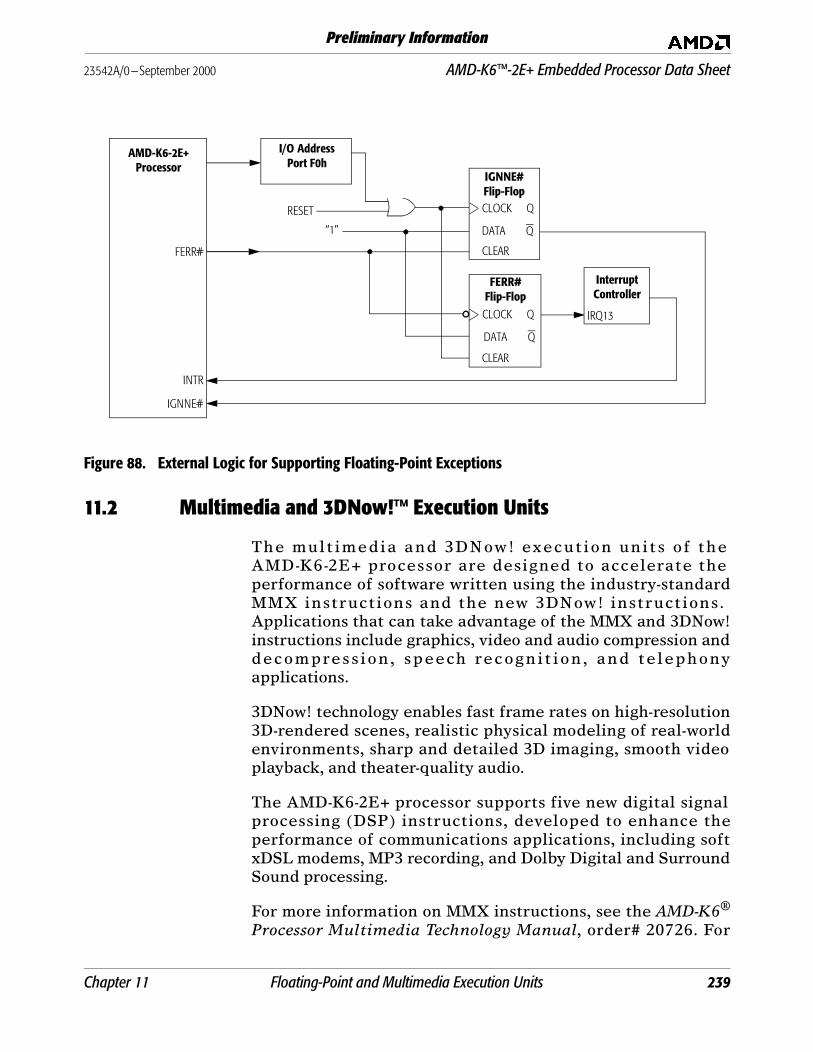
23542A/0—September 2000 AMD-K6™-2E+ Embedded Processor Data Sheet
Preliminary Information
Figure 88. External Logic for Supporting Floating-Point Exceptions
11.2 Multimedia and 3DNow!™ Execution Units
The mult imedia and 3DNow! execution units of theAMD-K6-2E+ processor are designed to accelerate theperformance of software written using the industry-standardMMX instructions and the new 3DNow! instructions.Applications that can take advantage of the MMX and 3DNow!instructions include graphics, video and audio compression anddecompress ion , speech recognit ion , and te lephonyapplications.
3DNow! technology enables fast frame rates on high-resolution3D-rendered scenes, realistic physical modeling of real-worldenvironments, sharp and detailed 3D imaging, smooth videoplayback, and theater-quality audio.
The AMD-K6-2E+ processor supports five new digital signalprocessing (DSP) instructions, developed to enhance theperformance of communications applications, including softxDSL modems, MP3 recording, and Dolby Digital and SurroundSound processing.
For more information on MMX instructions, see the AMD-K6®
Processor Multimedia Technology Manual, order# 20726. For
FERR# Flip-FlopCLOCK Q
DATA Q
CLEAR
IRQ13
Interrupt Controller
I/O AddressPort F0h
AMD-K6-2E+Processor
FERR#
INTR
IGNNE#
RESET
“1”
IGNNE# Flip-FlopCLOCK Q
DATA Q
CLEAR
Chapter 11 Floating-Point and Multimedia Execution Units 239
AMD-K6™-2E+ Embedded Processor Data Sheet 23542A/0—September 2000
Preliminary Information
more information on 3DNow! instructions, see the 3DNow!™Technology Manual, order# 21928. For more information on the3DNow! technology DSP extensions, see the AMD Extensions tothe 3DNow!™ and MMX™ Instructions Sets Manual, order#22466.
The multimedia execution unit can execute MMX instructionsin a single processor clock. All MMX and 3DNow! arithmeticinstructions are pipelined for higher performance. To increaseperformance, the processor is designed to simultaneouslydecode all MMX and 3DNow! instructions with most otherinstructions.
11.3 Floating-Point and MMX™/3DNow!™ Instruction Compatibility
Registers The eight 64-bit MMX registers (which are also utilized by3DNow! instructions) are mapped on the floating-point stack.This enables backward compatibility with all existing software.For example, the register saving event that is performed byoperating systems during task switching requires no changes tothe operating system. The same support provided in anoperating system’s interrupt 7 handler (Device Not Available)for saving and restoring the floating-point registers alsosupports saving and restoring the MMX registers.
Exceptions There are no new exceptions defined for supporting the MMXand 3DNow! instructions. All exceptions that occur whiledecoding or executing an MMX or 3DNow! instruction arehandled in existing exception handlers without modification.
FERR# and IGNNE# MMX instructions and 3DNow! instructions do not generatefloat ing-point exceptions . However, i f an unmaskedfloating-point exception is pending, the processor assertsFERR# at the instruction boundary of the next floating-pointinstruction, MMX instruction, 3DNow! instruction or WAITinstruction.
The sampling of IGNNE# asserted only affects processoroperation during the execution of an error-sensitivefloating-point instruction, MMX instruction, 3DNow!instruction or WAIT instruction when the NE bit in CR0 is setto 0.
240 Floating-Point and Multimedia Execution Units Chapter 11
23542A/0—September 2000 AMD-K6™-2E+ Embedded Processor Data Sheet
Preliminary Information
12 System Management Mode (SMM)
SMM is an alternate operating mode entered by way of a systemmanagement interrupt (SMI#) and handled by an interruptservice routine. SMM is designed for system control activitiessuch as power management. These activit ies appeartransparent to conventional operating systems like DOS andWindows. SMM is targeted for use by the Basic Input OutputSystem (BIOS), specialized low-level device drivers, and theoperating system. The code and data for SMM are stored in theSMM memory area, which is isolated from main memory.
The processor enters SMM by the assertion of the SMI#interrupt and the processor’s acknowledgment by the assertionof SMIACT#. At this point the processor saves its state into theSMM memory state-save area and jumps to the SMM serviceroutine. The processor returns from SMM when it executes theresume (RSM) instruction from within the SMM serviceroutine. Subsequently, the processor restores its state from theSMM save area, negates SMIACT#, and resumes execution withthe instruction following the point where it entered SMM.
The following sections summarize the SMM state-save area,entry into and exit from SMM, exceptions and interrupts inSMM, memory allocation and addressing in SMM, and the SMI#and SMIACT# signals.
12.1 SMM Operating Mode and Default Register Values
The software environment within SMM has the followingcharacteristics:
■ Addressing and operation in real mode
■ 4-Gbyte segment limits
■ Default 16-bit operand, address, and stack sizes, althoughinstruction prefixes can override these defaults
■ Control transfers that do not override the default operandsize truncate the EIP to 16 bits
■ Far jumps or calls cannot transfer control to a segment witha base address requiring more than 20 bits, as in real modesegment-base addressing
Chapter 12 System Management Mode (SMM) 241

AMD-K6™-2E+ Embedded Processor Data Sheet 23542A/0—September 2000
Preliminary Information
■ A20M# is masked
■ Interrupt vectors use the real-mode interrupt vector table
■ The IF flag in EFLAGS is cleared (INTR not recognized)
■ The TF flag in EFLAGS is cleared
■ The NMI and INIT interrupts are disabled
■ Debug register DR7 is cleared (debug traps disabled)
Figure 89 shows the default map of the SMM memory area. Itconsists of a 64-Kbyte area, between 0003_0000h and0003_FFFFh, of which the top 32 Kbytes (0003_8000h to0003_FFFFh) must be populated with RAM. The defaultcode-segment (CS) base address for the area—called the SMMbase address — is a t 0003_0000h. The top 512 bytes(0003_FE00h to 0003_FFFFh) contain a fill-down SMMstate-save area. The default entry point for the SMM serviceroutine is 0003_8000h.
Figure 89. SMM Memory
SMMState-Save
Area
SMM Base Address (CS)
Service Routine Entry Point
Fill Down
SMMService Routine
32-KbyteMinimum RAM
0003_8000h
0003_FE00h
0003_FFFFh
0003_0000h
242 System Management Mode (SMM) Chapter 12
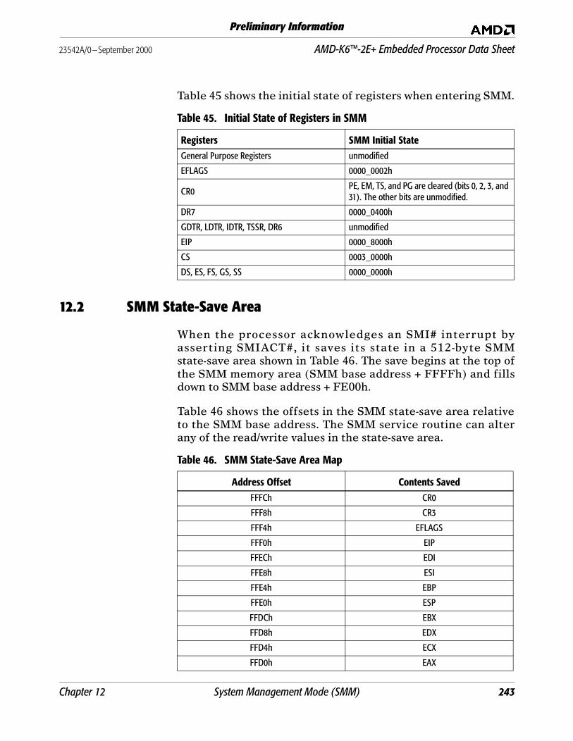
23542A/0—September 2000 AMD-K6™-2E+ Embedded Processor Data Sheet
Preliminary Information
Table 45 shows the initial state of registers when entering SMM.
12.2 SMM State-Save Area
When the processor acknowledges an SMI# interrupt byasserting SMIACT#, it saves its state in a 512-byte SMMstate-save area shown in Table 46. The save begins at the top ofthe SMM memory area (SMM base address + FFFFh) and fillsdown to SMM base address + FE00h.
Table 46 shows the offsets in the SMM state-save area relativeto the SMM base address. The SMM service routine can alterany of the read/write values in the state-save area.
Table 45. Initial State of Registers in SMM
Registers SMM Initial StateGeneral Purpose Registers unmodified
EFLAGS 0000_0002h
CR0PE, EM, TS, and PG are cleared (bits 0, 2, 3, and 31). The other bits are unmodified.
DR7 0000_0400h
GDTR, LDTR, IDTR, TSSR, DR6 unmodified
EIP 0000_8000h
CS 0003_0000h
DS, ES, FS, GS, SS 0000_0000h
Table 46. SMM State-Save Area Map
Address Offset Contents SavedFFFCh CR0
FFF8h CR3
FFF4h EFLAGS
FFF0h EIP
FFECh EDI
FFE8h ESI
FFE4h EBP
FFE0h ESP
FFDCh EBX
FFD8h EDX
FFD4h ECX
FFD0h EAX
Chapter 12 System Management Mode (SMM) 243
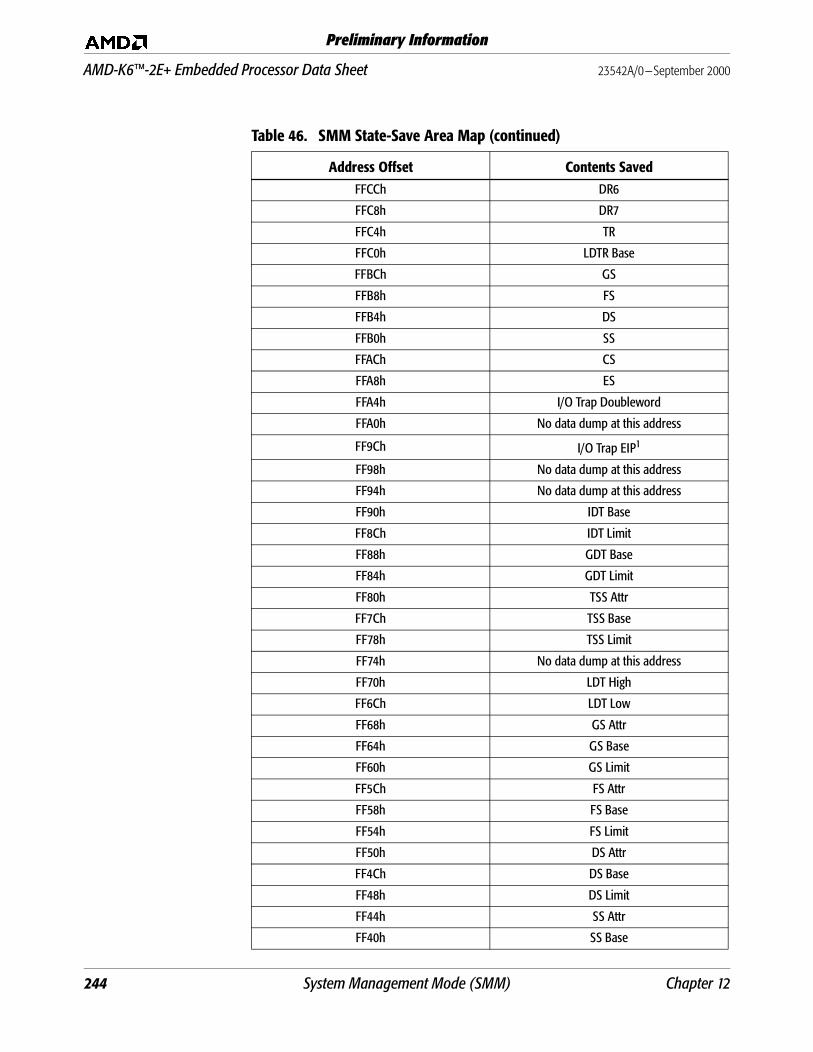
AMD-K6™-2E+ Embedded Processor Data Sheet 23542A/0—September 2000
Preliminary Information
FFCCh DR6
FFC8h DR7
FFC4h TR
FFC0h LDTR Base
FFBCh GS
FFB8h FS
FFB4h DS
FFB0h SS
FFACh CS
FFA8h ES
FFA4h I/O Trap Doubleword
FFA0h No data dump at this address
FF9Ch I/O Trap EIP1
FF98h No data dump at this address
FF94h No data dump at this address
FF90h IDT Base
FF8Ch IDT Limit
FF88h GDT Base
FF84h GDT Limit
FF80h TSS Attr
FF7Ch TSS Base
FF78h TSS Limit
FF74h No data dump at this address
FF70h LDT High
FF6Ch LDT Low
FF68h GS Attr
FF64h GS Base
FF60h GS Limit
FF5Ch FS Attr
FF58h FS Base
FF54h FS Limit
FF50h DS Attr
FF4Ch DS Base
FF48h DS Limit
FF44h SS Attr
FF40h SS Base
Table 46. SMM State-Save Area Map (continued)
Address Offset Contents Saved
244 System Management Mode (SMM) Chapter 12
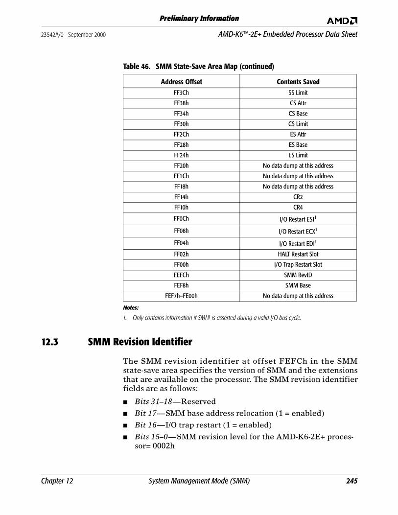
23542A/0—September 2000 AMD-K6™-2E+ Embedded Processor Data Sheet
Preliminary Information
12.3 SMM Revision Identifier
The SMM revision identifier at offset FEFCh in the SMMstate-save area specifies the version of SMM and the extensionsthat are available on the processor. The SMM revision identifierfields are as follows:
■ Bits 31–18—Reserved
■ Bit 17—SMM base address relocation (1 = enabled)
■ Bit 16—I/O trap restart (1 = enabled)
■ Bits 15–0—SMM revision level for the AMD-K6-2E+ proces-sor= 0002h
FF3Ch SS Limit
FF38h CS Attr
FF34h CS Base
FF30h CS Limit
FF2Ch ES Attr
FF28h ES Base
FF24h ES Limit
FF20h No data dump at this address
FF1Ch No data dump at this address
FF18h No data dump at this address
FF14h CR2
FF10h CR4
FF0Ch I/O Restart ESI1
FF08h I/O Restart ECX1
FF04h I/O Restart EDI1
FF02h HALT Restart Slot
FF00h I/O Trap Restart Slot
FEFCh SMM RevID
FEF8h SMM Base
FEF7h–FE00h No data dump at this address
Notes:
1. Only contains information if SMI# is asserted during a valid I/O bus cycle.
Table 46. SMM State-Save Area Map (continued)
Address Offset Contents Saved
Chapter 12 System Management Mode (SMM) 245

AMD-K6™-2E+ Embedded Processor Data Sheet 23542A/0—September 2000
Preliminary Information
Table 47 shows the format of the SMM Revision Identifier.
12.4 SMM Base Address
During RESET, the processor sets the base address of thecode-segment (CS) for the SMM memory area—the SMM baseaddress—to its default, 0003_0000h. The SMM base address atoffset FEF8h in the SMM state-save area can be changed by theSMM service routine to any address that is aligned to a32-Kbyte boundary. (Locations not aligned to a 32-Kbyteboundary cause the processor to enter the Shutdown state whenexecuting the RSM instruction.)
In some operating environments it may be desirable to relocatethe 64-Kbyte SMM memory area to a high memory area in orderto provide more low memory for legacy software. During systeminitialization, the base of the 64-Kbyte SMM memory area isrelocated by the BIOS. To relocate the SMM base address, thesystem enters the SMM handler at the default address. Thishandler changes the SMM base address location in the SMMstate-save area, copies the SMM handler to the new location,and exits SMM.
The next time SMM is entered, the processor saves its state atthe new base address. This new address is used for every SMMentry until the SMM base address in the SMM state-save area ischanged or a hardware reset occurs.
12.5 Halt Restart Slot
During entry into SMM, the halt restart slot at offset FF02h inthe SMM state-save area indicates if SMM was entered from theHalt state. Before returning from SMM, the halt restart slot(offset FF02h) can be written to by the SMM service routine tospecify whether the return from SMM takes the processor backto the Halt state or to the next instruction after the HLTinstruction.
Table 47. SMM Revision Identifier
31–18 17 16 15–0Reserved SMM Base Relocation I/O Trap Extension SMM Revision Level
0 1 1 0002h
246 System Management Mode (SMM) Chapter 12
23542A/0—September 2000 AMD-K6™-2E+ Embedded Processor Data Sheet
Preliminary Information
Upon entry into SMM, the halt restart slot is defined as follows:
■ Bits 15–1—Reserved
■ Bit 0—Point of entry to SMM:
1 = entered from Halt state
0 = not entered from Halt state
After entry into the SMI handler and before returning fromSMM, the halt restart slot can be written using the followingdefinition:
■ Bits 15–1—Reserved
■ Bit 0—Point of return when exiting from SMM:
1 = return to Halt state
0 = return to next instruction after the HLT instruction
If the return from SMM takes the processor back to the Haltstate, the HLT instruction is not re-executed, but the Haltspecial bus cycle is driven on the bus after the return.
12.6 I/O Trap Doubleword
If the assertion of SMI# is recognized during the execution of anI/O instruction, the I/O trap doubleword at offset FFA4h in theSMM state-save area contains information about theinstruction. The fields of the I/O trap doubleword areconfigured as follows:
■ Bits 31–16—I/O port address
■ Bits 15–4—Reserved
■ Bit 3—REP (repeat) string operation (1 = REP string, 0 = not a REP string)
■ Bit 2—I/O string operation (1 = I/O string, 0 = not an I/O string)
■ Bit 1—Valid I/O instruction (1 = valid, 0 = invalid)
■ Bit 0—Input or output instruction (1 = INx, 0 = OUTx)
Chapter 12 System Management Mode (SMM) 247

AMD-K6™-2E+ Embedded Processor Data Sheet 23542A/0—September 2000
Preliminary Information
Table 48 shows the format of the I/O trap doubleword.
The I/O trap doubleword is related to the I/O trap restart slot(see “I/O Trap Restart Slot”). If bit 1 of the I/O trap doublewordis set by the processor, it means that SMI# was asserted duringthe execution of an I/O instruction. The SMI handler tests bit 1to see if there is a valid I/O instruction trapped. If the I/Oinstruction is valid, the SMI handler is required to ensure theI/O trap restart slot is set properly. The I/O trap restart slotinforms the processor whether it should re-execute the I/Oinstruction after the RSM or execute the instruction followingthe trapped I/O instruction.
Note: If SMI# is sampled asserted during an I/O bus cycle aminimum of three clock edges before BRDY# is sampledasserted, the associated I/O instruction is guaranteed to betrapped by the SMI handler.
12.7 I/O Trap Restart Slot
The I/O trap restart slot at offset FF00h in the SMM state-savearea specifies whether the trapped I/O instruction should bere-executed on return from SMM. This slot in the state-save areais called the I/O instruction restart function. Re-executing atrapped I/O instruction is useful, for example, if an I/O writeoccurs to a disk that is powered down. The system logicmonitoring such an access can assert SMI#. Then the SMMservice routine would query the system logic, detect a failed I/Owrite, take action to power-up the I/O device, enable the I/Otrap restart slot feature, and return from SMM.
The fields of the I/O trap restart slot are defined as follows:
■ Bits 31–16—Reserved
■ Bits 15–0—I/O instruction restart on return from SMM:
0000h = execute the next instruction after the trapped I/O instruction
00FFh = re-execute the trapped I/O instruction
Table 48. I/O Trap Doubleword Configuration
31—16 15—4 3 2 1 0I/O Port Address
ReservedREP StringOperation
I/O String Operation
Valid I/O Instruction
Input or Output
248 System Management Mode (SMM) Chapter 12

23542A/0—September 2000 AMD-K6™-2E+ Embedded Processor Data Sheet
Preliminary Information
Table 49 shows the format of the I/O trap restart slot.
The processor initializes the I/O trap restart slot to 0000h uponentry into SMM. If SMM was entered due to a trapped I/Oinstruction, the processor indicates the validity of the I/Oinstruction by setting or clearing bit 1 of the I/O trapdoubleword at offset FFA4h in the SMM state-save area. TheSMM service routine should test bit 1 of the I/O trapdoubleword to determine if a valid I/O instruction was beingexecuted when entering SMM and before writing the I/O traprestart slot. If the I/O instruction is valid, the SMM serviceroutine can safely rewrite the I/O trap restart slot with the value00FFh, which causes the processor to re-execute the trapped I/Oinstruction when the RSM instruction is executed. If the I/Oinstruction is invalid, writing the I/O trap restart slot hasundefined results.
If a second SMI# is asserted and a valid I/O instruction wastrapped by the first SMM handler, the processor services thesecond SMI# prior to re-executing the trapped I/O instruction.The second entry into SMM never has bit 1 of the I/O trapdoubleword set, and the second SMM service routine must notrewrite the I/O trap restart slot.
During a simultaneous SMI# I/O instruction trap and debugbreakpoint trap, the AMD-K6-2E+ processor first responds tothe SMI# and postpones recognizing the debug exception untilafter returning from SMM via the RSM instruction. If the debugregisters DR3–DR0 are used while in SMM, they must be savedand restored by the SMM handler. The processor automaticallysaves and restores DR7–DR6. If the I/O trap restart slot in theSMM state-save area contains the value 00FFh when the RSMinstruction is executed, the debug trap does not occur untilafter the I/O instruction is re-executed.
Table 49. I/O Trap Restart Slot
31–16 15–0Reserved I/O Instruction restart on return from SMM:
0000h = execute the next instruction after the trapped I/O
00FFh = re-execute the trapped I/O instruction
Chapter 12 System Management Mode (SMM) 249
AMD-K6™-2E+ Embedded Processor Data Sheet 23542A/0—September 2000
Preliminary Information
12.8 Exceptions, Interrupts, and Debug in SMM
During an SMI# I/O trap, the exception/interrupt priority of theAMD-K6-2E+ processor changes from its normal priority. Thenormal priority places the debug traps at a priority higher thanthe sampling of the FLUSH# or SMI# signals. However, duringan SMI# I/O trap, the sampling of the FLUSH# or SMI# signalstakes precedence over debug traps.
The processor recognizes the assertion of NMI within SMMimmediately after the completion of an IRET instruction. OnceNMI is recognized within SMM, NMI recognition remainsenabled until SMM is exited, at which point NMI masking isrestored to the state it was in before entering SMM.
250 System Management Mode (SMM) Chapter 12
23542A/0—September 2000 AMD-K6™-2E+ Embedded Processor Data Sheet
Preliminary Information
13 Test and Debug
The AMD-K6-2E+ processor implements various test and debugmodes to enable the functional and manufacturing testing ofsystems and boards that use the processor. In addition, thedebug features of the processor allow designers to debug theinstruction execution of software components. This chapterdescribes the following test and debug features:
■ Built-In Self-Test (BIST)—The BIST, which is invoked afterthe falling transition of RESET, runs internal tests thatexercise most on-chip RAM structures.
■ Three-State Test Mode—A test mode that causes theprocessor to float its output and bidirectional pins.
■ Boundary-Scan Test Access Port (TAP)—The Joint TestAction Group (JTAG) test access function defined by theIEEE Standard Test Access Port and Boundary-ScanArchitecture (IEEE 1149.1-1990) specification.
■ Cache Inhibit—A feature that disables the processor’sinternal L1 and L2 caches.
■ Level-2 Cache Array Access Register (L2AAR)—TheAMD-K6-2E+ processor provides the L2AAR that allows fordirect access to the L2 cache and L2 tag arrays.
■ Debug Support—Consists of all x86-compatible softwaredebug features, including the debug extensions.
13.1 Built-In Self-Test (BIST)
Following the falling transition of RESET, the processorunconditionally runs its built-in self test (BIST). The internalresources tested during BIST include the following:
■ L1 instruction and data caches
■ L2 cache
■ Instruction and Data Translation Lookaside Buffers (TLBs)
Chapter 13 Test and Debug 251

AMD-K6™-2E+ Embedded Processor Data Sheet 23542A/0—September 2000
Preliminary Information
The contents of the EAX general-purpose register after thecompletion of reset indicate if the BIST was successful.
■ If EAX contains 0000_0000h, then BIST was successful.
■ If EAX is non-zero, the BIST failed.
Following the completion of the BIST, the processor jumps toaddress FFFF_FFF0h to start instruction execution, regardlessof the outcome of the BIST.
The BIST takes approximately 5,000,000 processor clocks tocomplete.
13.2 Three-State Test Mode
The Three-State Test mode causes the processor to float itsoutput and bidirectional pins, which is useful for board-levelmanufacturing testing. In this mode, the processor iselectrically isolated from other components on a system board,allowing automated test equipment (ATE) to test componentsthat drive the same signals as those the processor floats.
If the FLUSH# signal is sampled Low during the fallingtransition of RESET, the processor enters the Three-State Testmode. (See “FLUSH# (Cache Flush)” on page 112 for thespecific sampling requirements.) The signals floated in theThree-State Test mode are as follows:
The VCC2DET, VCC2H/L#, and TDO signals are the onlyoutputs not floated in the Three-State Test mode.
■ VCC2DET and VCC2H/L# must remain Low to ensure thesystem continues to supply the specified processor corevoltage to the VCC2 pins.
■ A[31:3] ■ D/C# ■ M/IO#
■ ADS# ■ D[63:0] ■ PCD
■ ADSC# ■ DP[7:0] ■ PCHK#
■ AP ■ FERR# ■ PWT
■ APCHK# ■ HIT# ■ SCYC
■ BE[7:0]# ■ HITM# ■ SMIACT#
■ BREQ ■ HLDA ■ VID[4:0]
■ CACHE# ■ LOCK# ■ W/R#
252 Test and Debug Chapter 13
23542A/0—September 2000 AMD-K6™-2E+ Embedded Processor Data Sheet
Preliminary Information
■ TDO is never floated because the Boundary-Scan TestAccess Port must remain enabled at all times, includingduring the Three-State Test mode.
The Three-State Test mode is exited when the processorsamples RESET asserted.
13.3 Boundary-Scan Test Access Port (TAP)
The boundary-scan Test Access Port (TAP) is an IEEE standardthat defines synchronous scanning test methods for complexlogic circuits, such as boards containing a processor. TheAMD-K6-2E+ processor supports the TAP standard defined inthe IEEE Standard Test Access Port and Boundary-ScanArchitecture (IEEE 1149.1-1990) specification.
Boundary scan testing uses a shift register consisting of theserial interconnection of boundary-scan cells that correspond toeach I/O buffer of the processor. This non-inverting registerchain, called a Boundary Scan Register (BSR), can be used tocapture the state of every processor pin and to drive everyprocessor output and bidirectional pin to a known state.
Each BSR of every component on a board that implements theboundary-scan architecture can be serially interconnected toenable component interconnect testing.
Test Access Port The TAP consists of the following:
■ Test Access Port (TAP) Controller—The TAP controller is asynchronous, finite state machine that uses the TMS andTDI input signals to control a sequence of test operations.See “TAP Controller State Machine” on page 260 for a list ofTAP states and their definition.
■ Instruction Register (IR)—The IR contains the instructionsthat select the test operation to be performed and the TestData Register (TDR) to be selected. See “TAP Registers” onpage 255 for more details on the IR.
■ Test Data Registers (TDR)—The three TDRs are used toprocess the test data. Each TDR is selected by an instructionin the Instruction Register (IR). See “TAP Registers” onpage 255 for a list of these registers and their functions.
Chapter 13 Test and Debug 253
AMD-K6™-2E+ Embedded Processor Data Sheet 23542A/0—September 2000
Preliminary Information
TAP Signals The test signals associated with the TAP controller are asfollows:
■ TCK—The Test Clock for all TAP operations. The risingedge of TCK is used for sampling TAP signals, and thefalling edge of TCK is used for asserting TAP signals. Thestate of the TMS signal sampled on the rising edge of TCKcauses the state transitions of the TAP controller to occur.TCK can be stopped in the logic 0 or 1 state.
■ TDI—The Test Data Input represents the input to the mostsignificant bit of all TAP registers, including the IR and alltest data registers. Test data and instructions are seriallyshifted by one bit into their respective registers on the risingedge of TCK.
■ TDO—The Test Data Output represents the output of theleast significant bit of all TAP registers, including the IR andall test data registers. Test data and instructions are seriallyshifted by one bit out of their respective registers on thefalling edge of TCK.
■ TMS—The Test Mode Select input specifies the testfunction and sequence of state changes for boundary-scantesting. If TMS is sampled High for five or more consecutiveclocks, the TAP controller enters its reset state.
■ TRST#—The Test Reset signal is an asynchronous reset thatunconditionally causes the TAP controller to enter its resetstate.
Refer to “Electrical Data” on page 285 and “Signal SwitchingCharacteristics” on page 295 to obtain the electricalspecifications of the test signals.
254 Test and Debug Chapter 13
23542A/0—September 2000 AMD-K6™-2E+ Embedded Processor Data Sheet
Preliminary Information
TAP Registers The AMD-K6-2E+ processor provides an Instruction Register(IR) and three Test Data Registers (TDR) to support theboundary-scan architecture. The IR and one of the TDRs—theBoundary-Scan Register (BSR)—consist of a shift register andan output register. The shift register is loaded in parallel in theCapture states. (See “TAP Controller State Machine” onpage 260 for a description of the TAP controller states.) Inaddition, the shift register is loaded and shifted serially in theShift states. The output register is loaded in parallel from itscorresponding shift register in the Update states.
Instruction Register (IR). The IR is a 5-bit register, without parity,that determines which instruction to run and which test dataregister to select. When the TAP controller enters theCapture-IR state, the processor loads the following bits into theIR shift register:
■ 01b—Loaded into the two least significant bits, as specifiedby the IEEE 1149.1 standard
■ 000b—Loaded into the three most significant bits
Loading 00001b into the IR shift register during the Capture-IRstate results in loading the SAMPLE/PRELOAD instruction.
For each entry into the Shift-IR state, the IR shift register isserially shifted by one bit toward the TDO pin. During the shift,the most significant bit of the IR shift register is loaded fromthe TDI pin.
The IR output register is loaded from the IR shift register in theUpdate-IR state, and the current instruction is defined by theIR output register. See “TAP Instructions” on page 259 for a listand definit ion of the instruct ions supported by theAMD-K6-2E+ processor.
Boundary Scan Register (BSR). The Boundary Scan Register is a TestData Register consisting of the interconnection of 152boundary-scan cells. Each output and bidirectional pin of theprocessor requires a two-bit cell, where one bit corresponds tothe pin and the other bit is the output enable for the pin. Whena 0 is shifted into the enable bit of a cell, the corresponding pinis floated, and when a 1 is shifted into the enable bit, the pin isdriven valid. Each input pin requires a one-bit cell thatcorresponds to the pin. The last cell of the BSR is reserved anddoes not correspond to any processor pin.
Chapter 13 Test and Debug 255
AMD-K6™-2E+ Embedded Processor Data Sheet 23542A/0—September 2000
Preliminary Information
The total number of bits that comprise the BSR is 297. Table 50on page 257 lists the order of these bits, where TDI is the inputto bit 296, and TDO is driven from the output of bit 0. Theentries listed as pin_E (where pin is an output or bidirectionalsignal) are the enable bits.
If the BSR is the register selected by the current instructionand the TAP controller is in the Capture-DR state, the processorloads the BSR shift register as follows:
■ If the current instruction is SAMPLE/PRELOAD, then thecurrent state of each input, output, and bidirectional pin isloaded. A bidirectional pin is treated as an output if itsenable bit equals 1, and it is treated as an input if its enablebit equals 0.
■ If the current instruction is EXTEST, then the current stateof each input pin is loaded. A bidirectional pin is treated asan input, regardless of the state of its enable.
While in the Shift-DR state, the BSR shift register is seriallyshifted toward the TDO pin. During the shift, bit 280 of the BSRis loaded from the TDI pin.
The BSR output register is loaded with the contents of the BSRshift register in the Update-DR state. If the current instructionis EXTEST, the processor’s output pins, as well as thosebidirectional pins that are enabled as outputs, are driven withtheir corresponding values from the BSR output register.
256 Test and Debug Chapter 13
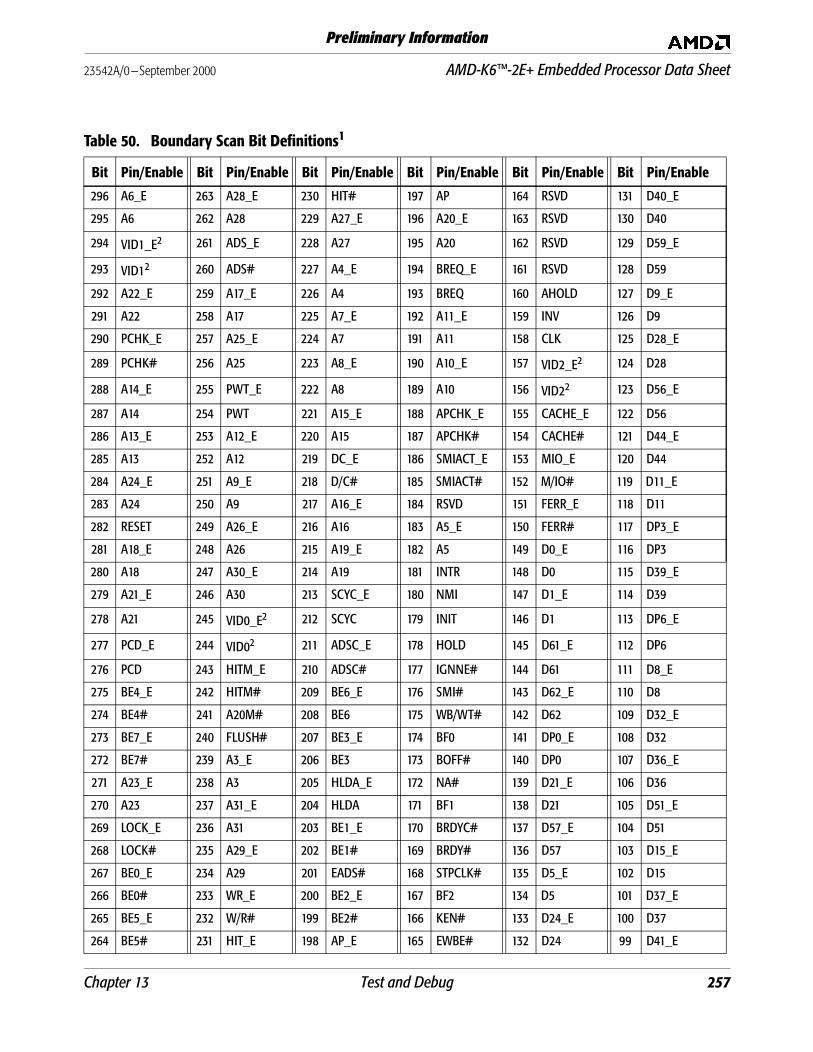
23542A/0—September 2000 AMD-K6™-2E+ Embedded Processor Data Sheet
Preliminary Information
Table 50. Boundary Scan Bit Definitions1
Bit Pin/Enable Bit Pin/Enable Bit Pin/Enable Bit Pin/Enable Bit Pin/Enable Bit Pin/Enable
296 A6_E 263 A28_E 230 HIT# 197 AP 164 RSVD 131 D40_E
295 A6 262 A28 229 A27_E 196 A20_E 163 RSVD 130 D40
294 VID1_E2 261 ADS_E 228 A27 195 A20 162 RSVD 129 D59_E
293 VID12 260 ADS# 227 A4_E 194 BREQ_E 161 RSVD 128 D59
292 A22_E 259 A17_E 226 A4 193 BREQ 160 AHOLD 127 D9_E
291 A22 258 A17 225 A7_E 192 A11_E 159 INV 126 D9
290 PCHK_E 257 A25_E 224 A7 191 A11 158 CLK 125 D28_E
289 PCHK# 256 A25 223 A8_E 190 A10_E 157 VID2_E2 124 D28
288 A14_E 255 PWT_E 222 A8 189 A10 156 VID22 123 D56_E
287 A14 254 PWT 221 A15_E 188 APCHK_E 155 CACHE_E 122 D56
286 A13_E 253 A12_E 220 A15 187 APCHK# 154 CACHE# 121 D44_E
285 A13 252 A12 219 DC_E 186 SMIACT_E 153 MIO_E 120 D44
284 A24_E 251 A9_E 218 D/C# 185 SMIACT# 152 M/IO# 119 D11_E
283 A24 250 A9 217 A16_E 184 RSVD 151 FERR_E 118 D11
282 RESET 249 A26_E 216 A16 183 A5_E 150 FERR# 117 DP3_E
281 A18_E 248 A26 215 A19_E 182 A5 149 D0_E 116 DP3
280 A18 247 A30_E 214 A19 181 INTR 148 D0 115 D39_E
279 A21_E 246 A30 213 SCYC_E 180 NMI 147 D1_E 114 D39
278 A21 245 VID0_E2 212 SCYC 179 INIT 146 D1 113 DP6_E
277 PCD_E 244 VID02 211 ADSC_E 178 HOLD 145 D61_E 112 DP6
276 PCD 243 HITM_E 210 ADSC# 177 IGNNE# 144 D61 111 D8_E
275 BE4_E 242 HITM# 209 BE6_E 176 SMI# 143 D62_E 110 D8
274 BE4# 241 A20M# 208 BE6 175 WB/WT# 142 D62 109 D32_E
273 BE7_E 240 FLUSH# 207 BE3_E 174 BF0 141 DP0_E 108 D32
272 BE7# 239 A3_E 206 BE3 173 BOFF# 140 DP0 107 D36_E
271 A23_E 238 A3 205 HLDA_E 172 NA# 139 D21_E 106 D36
270 A23 237 A31_E 204 HLDA 171 BF1 138 D21 105 D51_E
269 LOCK_E 236 A31 203 BE1_E 170 BRDYC# 137 D57_E 104 D51
268 LOCK# 235 A29_E 202 BE1# 169 BRDY# 136 D57 103 D15_E
267 BE0_E 234 A29 201 EADS# 168 STPCLK# 135 D5_E 102 D15
266 BE0# 233 WR_E 200 BE2_E 167 BF2 134 D5 101 D37_E
265 BE5_E 232 W/R# 199 BE2# 166 KEN# 133 D24_E 100 D37
264 BE5# 231 HIT_E 198 AP_E 165 EWBE# 132 D24 99 D41_E
Chapter 13 Test and Debug 257
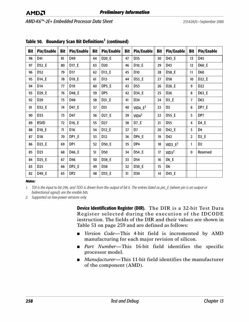
AMD-K6™-2E+ Embedded Processor Data Sheet 23542A/0—September 2000
Preliminary Information
Device Identification Register (DIR). The DIR is a 32-bit Test DataRegister selected during the execution of the IDCODEinstruction. The fields of the DIR and their values are shown inTable 51 on page 259 and are defined as follows:
■ Version Code—This 4-bit field is incremented by AMDmanufacturing for each major revision of silicon.
■ Part Number—This 16-bit field identifies the specificprocessor model.
■ Manufacturer—This 11-bit field identifies the manufacturerof the component (AMD).
98 D41 81 D49 64 D20_E 47 D35 30 D43_E 13 D45
97 D52_E 80 D17_E 63 D20 46 D10_E 29 D43 12 D60_E
96 D52 79 D17 62 D13_E 45 D10 28 D58_E 11 D60
95 D14_E 78 D19_E 61 D13 44 D53_E 27 D58 10 D22_E
94 D14 77 D19 60 DP5_E 43 D53 26 D26_E 9 D22
93 D29_E 76 D48_E 59 DP5 42 D34_E 25 D26 8 D63_E
92 D29 75 D48 58 D31_E 41 D34 24 D3_E 7 D63
91 D33_E 74 D47_E 57 D31 40 VID4_E2 23 D3 6 DP7_E
90 D33 73 D47 56 D27_E 39 VID42 22 D55_E 5 DP7
89 RSVD 72 D16_E 55 D27 38 D7_E 21 D55 4 D4_E
88 D18_E 71 D16 54 D12_E 37 D7 20 D42_E 3 D4
87 D18 70 DP1_E 53 D12 36 DP4_E 19 D42 2 D2_E
86 D23_E 69 DP1 52 D50_E 35 DP4 18 VID3_E2 1 D2
85 D23 68 D46_E 51 D50 34 D54_E 17 VID32 0 Reserved
84 D25_E 67 D46 50 D38_E 33 D54 16 D6_E
83 D25 66 DP2_E 49 D38 32 D30_E 15 D6
82 D49_E 65 DP2 48 D35_E 31 D30 14 D45_E
Notes:
1. TDI is the input to bit 296, and TDO is driven from the output of bit 0. The entries listed as pin_E (where pin is an output or bidirectional signal) are the enable bits.
2. Supported on low-power versions only.
Table 50. Boundary Scan Bit Definitions1 (continued)
Bit Pin/Enable Bit Pin/Enable Bit Pin/Enable Bit Pin/Enable Bit Pin/Enable Bit Pin/Enable
258 Test and Debug Chapter 13
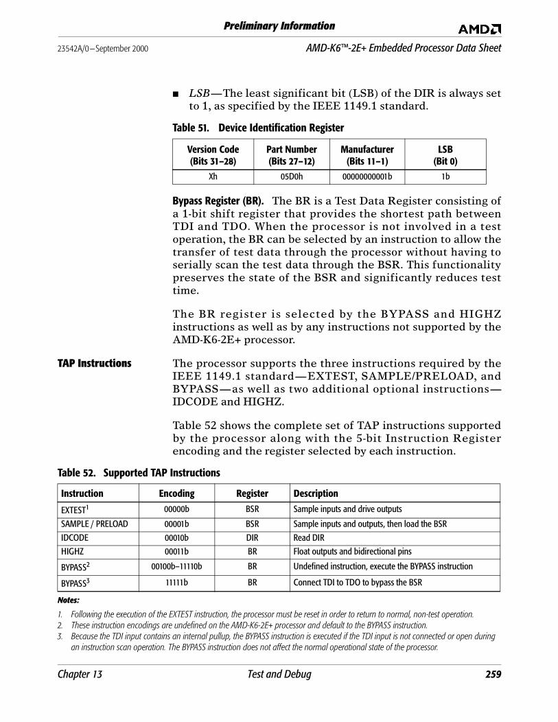
23542A/0—September 2000 AMD-K6™-2E+ Embedded Processor Data Sheet
Preliminary Information
■ LSB—The least significant bit (LSB) of the DIR is always setto 1, as specified by the IEEE 1149.1 standard.
Bypass Register (BR). The BR is a Test Data Register consisting ofa 1-bit shift register that provides the shortest path betweenTDI and TDO. When the processor is not involved in a testoperation, the BR can be selected by an instruction to allow thetransfer of test data through the processor without having toserially scan the test data through the BSR. This functionalitypreserves the state of the BSR and significantly reduces testtime.
The BR register is selected by the BYPASS and HIGHZinstructions as well as by any instructions not supported by theAMD-K6-2E+ processor.
TAP Instructions The processor supports the three instructions required by theIEEE 1149.1 standard—EXTEST, SAMPLE/PRELOAD, andBYPASS—as well as two additional optional instructions—IDCODE and HIGHZ.
Table 52 shows the complete set of TAP instructions supportedby the processor along with the 5-bit Instruction Registerencoding and the register selected by each instruction.
Table 51. Device Identification Register
Version Code(Bits 31–28)
Part Number(Bits 27–12)
Manufacturer(Bits 11–1)
LSB(Bit 0)
Xh 05D0h 00000000001b 1b
Table 52. Supported TAP Instructions
Instruction Encoding Register Description
EXTEST1 00000b BSR Sample inputs and drive outputs
SAMPLE / PRELOAD 00001b BSR Sample inputs and outputs, then load the BSR
IDCODE 00010b DIR Read DIR
HIGHZ 00011b BR Float outputs and bidirectional pins
BYPASS2 00100b–11110b BR Undefined instruction, execute the BYPASS instruction
BYPASS3 11111b BR Connect TDI to TDO to bypass the BSR
Notes:
1. Following the execution of the EXTEST instruction, the processor must be reset in order to return to normal, non-test operation.2. These instruction encodings are undefined on the AMD-K6-2E+ processor and default to the BYPASS instruction.3. Because the TDI input contains an internal pullup, the BYPASS instruction is executed if the TDI input is not connected or open during
an instruction scan operation. The BYPASS instruction does not affect the normal operational state of the processor.
Chapter 13 Test and Debug 259

AMD-K6™-2E+ Embedded Processor Data Sheet 23542A/0—September 2000
Preliminary Information
EXTEST Instruction. When the EXTEST instruction is executed,the processor loads the BSR shift register with the current stateof the input and bidirectional pins in the Capture-DR state anddrives the output and bidirectional pins with the correspondingvalues from the BSR output register in the Update-DR state.
SAMPLE/PRELOAD Instruction. The SAMPLE/PRELOAD instructionperforms two functions. These functions are as follows:
■ During the Capture-DR state, the processor loads the BSRshift register with the current state of every input, output,and bidirectional pin.
■ During the Update-DR state, the BSR output register isloaded from the BSR shift register in preparation for thenext EXTEST instruction.
The SAMPLE/PRELOAD instruction does not affect the normaloperational state of the processor.
BYPASS Instruction. The BYPASS instruction selects the BRregister, which reduces the boundary-scan length through theprocessor from 297 to one (TDI to BR to TDO). The BYPASSinstruction does not affect the normal operational state of theprocessor.
IDCODE Instruction. The IDCODE instruction selects the DIRregister, allowing the device identification code to be shiftedout of the processor. This instruction is loaded into the IR whenthe TAP controller is reset. The IDCODE instruction does notaffect the normal operational state of the processor.
HIGHZ Instruction. The HIGHZ instruction forces all output andbidirectional pins to be floated. During this instruction, the BRis selected and the normal operational state of the processor isnot affected.
TAP Controller State Machine
The TAP controller state diagram is shown in Figure 90 on page261. State transitions occur on the rising edge of TCK. The logic0 or 1 next to the states represents the value of the TMS signalsampled by the processor on the rising edge of TCK.
260 Test and Debug Chapter 13
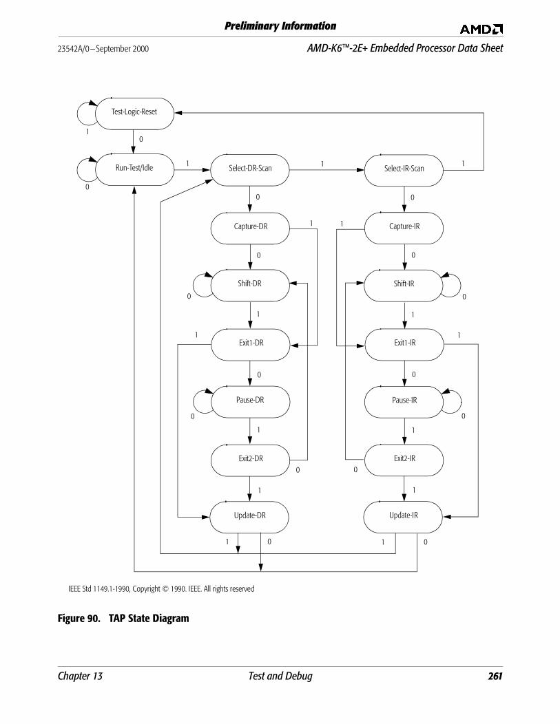
23542A/0—September 2000 AMD-K6™-2E+ Embedded Processor Data Sheet
Preliminary Information
Figure 90. TAP State Diagram
Test-Logic-Reset
Shift-DR
Pause-DR
Update-DR Update-IR
0
1
0
0
0
0
0
1 1
11 1
0
0
0
0
0
1 1
0 0
1 1
0
1 1
0
0
1
1 1
1
Run-Test/Idle
Exit2-IR
Exit1-IR
Pause-IR
Shift-IR
Select-DR-Scan Select-IR-Scan
Capture-DR Capture-IR
Exit1-DR
Exit2-DR
IEEE Std 1149.1-1990, Copyright © 1990. IEEE. All rights reserved
Chapter 13 Test and Debug 261
AMD-K6™-2E+ Embedded Processor Data Sheet 23542A/0—September 2000
Preliminary Information
The states of the TAP controller are described as follows:
Test-Logic-Reset. This state represents the initial reset state of theTAP controller and is entered when the processor samplesRESET asserted, when TRST# is asynchronously asserted, andwhen TMS is sampled High for five or more consecutive clocks.In addition, this state can be entered from the Select-IR-Scanstate. The IR is initialized with the IDCODE instruction, andthe processor’s normal operation is not affected in this state.
Capture-DR. During the SAMPLE/PRELOAD instruction, theprocessor loads the BSR shift register with the current state ofevery input, output, and bidirectional pin. During the EXTESTinstruction, the processor loads the BSR shift register with thecurrent state of every input and bidirectional pin.
Capture-IR. When the TAP controller enters the Capture-IR state,the processor loads 01b into the two least significant bits of theIR shift register and loads 000b into the three most significantbits of the IR shift register.
Shift-DR. While in the Shift-DR state, the selected TDR shiftregister is serially shifted toward the TDO pin. During the shift,the most significant bit of the TDR is loaded from the TDI pin.
Shift-IR. While in the Shift-IR state, the IR shift register isserially shifted toward the TDO pin. During the shift, the mostsignificant bit of the IR is loaded from the TDI pin.
Update-DR. During the SAMPLE/PRELOAD instruction, the BSRoutput register is loaded with the contents of the BSR shiftregister. During the EXTEST instruction, the output pins, aswell as those bidirectional pins defined as outputs, are drivenwith their corresponding values from the BSR output register.
Update-IR. In this state, the IR output register is loaded from theIR shift register, and the current instruction is defined by theIR output register.
262 Test and Debug Chapter 13
23542A/0—September 2000 AMD-K6™-2E+ Embedded Processor Data Sheet
Preliminary Information
The following states have no effect on the normal or testoperation of the processor other than as shown in Figure 90 onpage 261:
■ Run-Test/Idle—This state is an idle state between scanoperations.
■ Select-DR-Scan—This is the initial state of the test dataregister state transitions.
■ Select-IR-Scan—This is the initial state of the InstructionRegister state transitions.
■ Exit1-DR—This state is entered to terminate the shiftingprocess and enter the Update-DR state.
■ Exit1-IR—This state is entered to terminate the shiftingprocess and enter the Update-IR state.
■ Pause-DR—This state is entered to temporarily stop theshifting process of a Test Data Register.
■ Pause-IR—This state is entered to temporarily stop theshifting process of the Instruction Register.
■ Exit2-DR—This state is entered in order to either terminatethe shifting process and enter the Update-DR state or toresume shifting following the exit from the Pause-DR state.
■ Exit2-IR—This state is entered in order to either terminatethe shifting process and enter the Update-IR state or toresume shifting following the exit from the Pause-IR state.
13.4 Cache Inhibit
The AMD-K6-2E+ processor provides a means for inhibiting thenormal operation of its internal L1 and L2 caches while stillsupporting an external cache. This capability allows systemdesigners to disable the L1 and L2 caches during the testingand debug of an L3 cache.
If the Cache Inhibit bit (bit 3) of Test Register 12 (TR12) is setto 0, the processor’s L1 and L2 caches are enabled and operateas described in “Cache Organization” on page 205. If the CacheInhibit bit is set to 1, the L1 and L2 caches are disabled and nonew cache lines are allocated. Even though new allocations donot occur, valid L1 and L2 cache lines remain valid and are readby the processor when a requested address hits a cache line. Inaddition, the processor continues to support inquire cycles
Chapter 13 Test and Debug 263
AMD-K6™-2E+ Embedded Processor Data Sheet 23542A/0—September 2000
Preliminary Information
initiated by the system logic, including the execution ofwriteback cycles when a modified cache line is hit.
While the L1 and L2 are inhibited, the processor continues todrive the PCD output signal appropriately, which system logiccan use to control external L3 caching.
In order to completely disable the L1 and L2 caches so that novalid lines exist in the cache, the Cache Inhibit bit must be setto 1 and the cache must be flushed in one of the following ways:
■ Asserting the FLUSH# input signal
■ Executing the WBINVD instruction
■ Executing the INVD instruction (modified cache lines arenot written back to memory)
■ Using the Page Flush/Invalidate Register (PFIR) (see “PageFlush/Invalidate Register (PFIR)” on page 223)
13.5 L2 Cache and Tag Array Testing
Level-2 Cache Array Access Register (L2AAR)
The AMD-K6-2E+ processor provides the Level-2 Cache ArrayAccess Register (L2AAR) that allows for direct access to the L2cache and L2 tag arrays. The 128-Kbyte L2 cache in theAMD-K6-2E+ is organized as shown in Figure 91 on page 265:
■ Four 32-Kbyte ways
■ Each way contains 512sets
■ Each set contains four 64-byte sectors (one sector in eachway)
■ Each sector contains two 32-byte cache lines
■ Each cache line contains four 8-byte octets
■ Each octet contains an upper and lower dword (4 bytes)
Each line within a sector contains its own MESI state bits, andassociated with each sector is a tag and LRU (least recentlyused) information.
264 Test and Debug Chapter 13
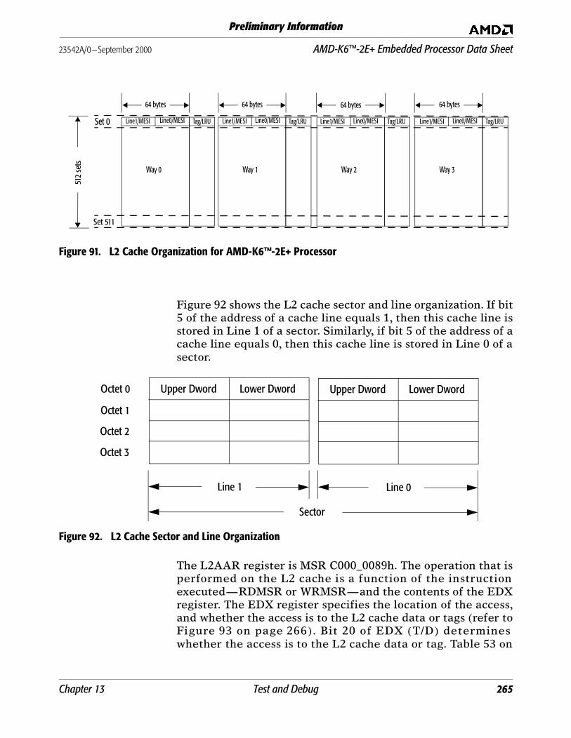
23542A/0—September 2000 AMD-K6™-2E+ Embedded Processor Data Sheet
Preliminary Information
Figure 91. L2 Cache Organization for AMD-K6™-2E+ Processor
Figure 92 shows the L2 cache sector and line organization. If bit5 of the address of a cache line equals 1, then this cache line isstored in Line 1 of a sector. Similarly, if bit 5 of the address of acache line equals 0, then this cache line is stored in Line 0 of asector.
Figure 92. L2 Cache Sector and Line Organization
The L2AAR register is MSR C000_0089h. The operation that isperformed on the L2 cache is a function of the instructionexecuted—RDMSR or WRMSR—and the contents of the EDXregister. The EDX register specifies the location of the access,and whether the access is to the L2 cache data or tags (refer toFigure 93 on page 266). Bit 20 of EDX (T/D) determineswhether the access is to the L2 cache data or tag. Table 53 on
512
sets
Set 0
64 bytes
Way 2
Line1/MESI Line0/MESI Tag/LRU
64 bytes
Way 1
Line1/MESI Line0/MESI Tag/LRU
64 bytes
Way 0
Line1/MESI Line0/MESI Tag/LRU
64 bytes
Way 3
Line1/MESI Line0/MESI Tag/LRU
Set 511
Upper Dword Lower DwordOctet 0
Line 1
Octet 1
Octet 2
Octet 3
Upper Dword Lower Dword
Line 0
Sector
Chapter 13 Test and Debug 265
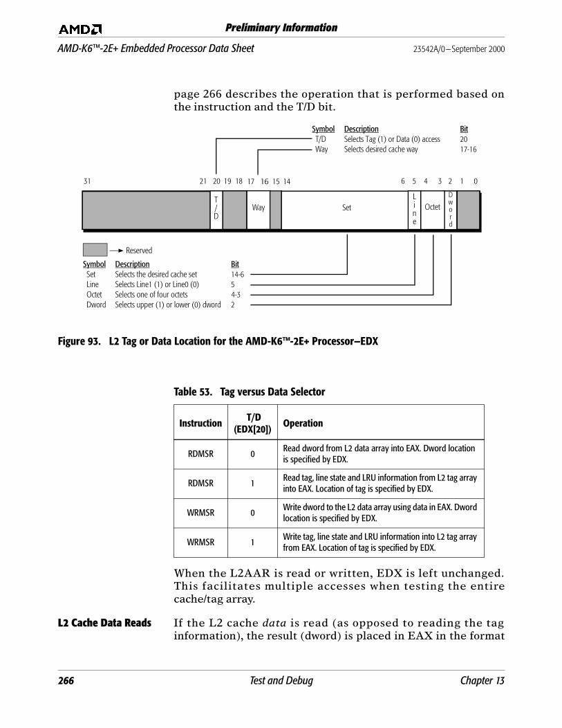
AMD-K6™-2E+ Embedded Processor Data Sheet 23542A/0—September 2000
Preliminary Information
page 266 describes the operation that is performed based onthe instruction and the T/D bit.
Figure 93. L2 Tag or Data Location for the AMD-K6™-2E+ Processor—EDX
When the L2AAR is read or written, EDX is left unchanged.This facilitates multiple accesses when testing the entirecache/tag array.
L2 Cache Data Reads If the L2 cache data is read (as opposed to reading the taginformation), the result (dword) is placed in EAX in the format
Reserved
0
Set
2131 20 19 17 16 51518
Way
4 3 2 16
Symbol Description BitSet Selects the desired cache set 14-6Line Selects Line1 (1) or Line0 (0) 5Octet Selects one of four octets 4-3Dword Selects upper (1) or lower (0) dword 2
Line
Octet
Dword
T/D
Symbol Description BitT/D Selects Tag (1) or Data (0) access 20Way Selects desired cache way 17-16
14
Table 53. Tag versus Data Selector
Instruction T/D(EDX[20]) Operation
RDMSR 0Read dword from L2 data array into EAX. Dword location is specified by EDX.
RDMSR 1Read tag, line state and LRU information from L2 tag array into EAX. Location of tag is specified by EDX.
WRMSR 0Write dword to the L2 data array using data in EAX. Dword location is specified by EDX.
WRMSR 1Write tag, line state and LRU information into L2 tag array from EAX. Location of tag is specified by EDX.
266 Test and Debug Chapter 13
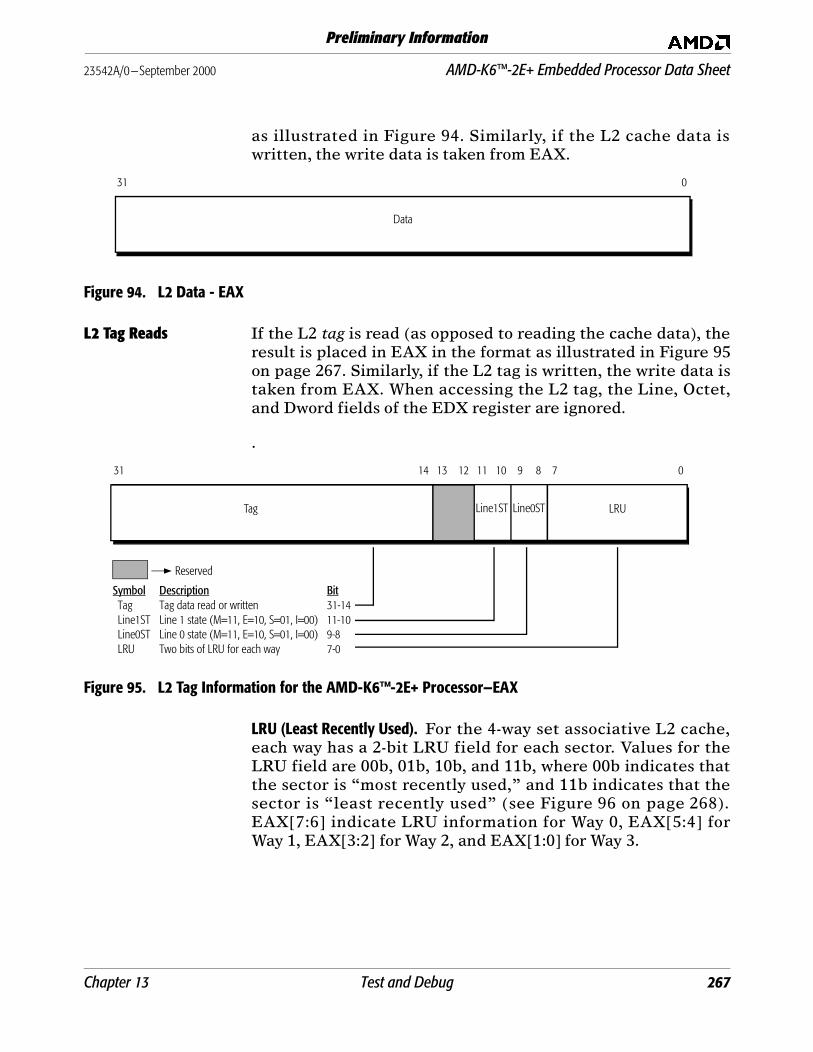
23542A/0—September 2000 AMD-K6™-2E+ Embedded Processor Data Sheet
Preliminary Information
as illustrated in Figure 94. Similarly, if the L2 cache data iswritten, the write data is taken from EAX.
Figure 94. L2 Data - EAX
L2 Tag Reads If the L2 tag is read (as opposed to reading the cache data), theresult is placed in EAX in the format as illustrated in Figure 95on page 267. Similarly, if the L2 tag is written, the write data istaken from EAX. When accessing the L2 tag, the Line, Octet,and Dword fields of the EDX register are ignored.
.
Figure 95. L2 Tag Information for the AMD-K6™-2E+ Processor—EAX
LRU (Least Recently Used). For the 4-way set associative L2 cache,each way has a 2-bit LRU field for each sector. Values for theLRU field are 00b, 01b, 10b, and 11b, where 00b indicates thatthe sector is “most recently used,” and 11b indicates that thesector is “least recently used” (see Figure 96 on page 268).EAX[7:6] indicate LRU information for Way 0, EAX[5:4] forWay 1, EAX[3:2] for Way 2, and EAX[1:0] for Way 3.
031
Data
CMD
Reserved
0
Tag
31 14 12 10 9 7811
LRULine0STLine1ST
Symbol Description BitTag Tag data read or written 31-14Line1ST Line 1 state (M=11, E=10, S=01, I=00) 11-10Line0ST Line 0 state (M=11, E=10, S=01, I=00) 9-8LRU Two bits of LRU for each way 7-0
13
Chapter 13 Test and Debug 267
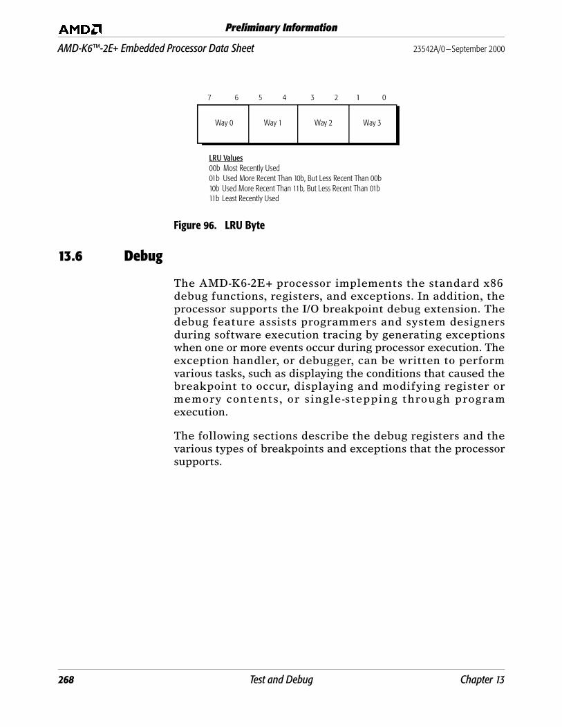
AMD-K6™-2E+ Embedded Processor Data Sheet 23542A/0—September 2000
Preliminary Information
Figure 96. LRU Byte
13.6 Debug
The AMD-K6-2E+ processor implements the standard x86debug functions, registers, and exceptions. In addition, theprocessor supports the I/O breakpoint debug extension. Thedebug feature assists programmers and system designersduring software execution tracing by generating exceptionswhen one or more events occur during processor execution. Theexception handler, or debugger, can be written to performvarious tasks, such as displaying the conditions that caused thebreakpoint to occur, displaying and modifying register ormemory contents, or single-stepping through programexecution.
The following sections describe the debug registers and thevarious types of breakpoints and exceptions that the processorsupports.
7 6 5 4 3 2 1 0
Way 2
LRU Values00b Most Recently Used01b Used More Recent Than 10b, But Less Recent Than 00b10b Used More Recent Than 11b, But Less Recent Than 01b11b Least Recently Used
Way 3Way 0 Way 1
268 Test and Debug Chapter 13
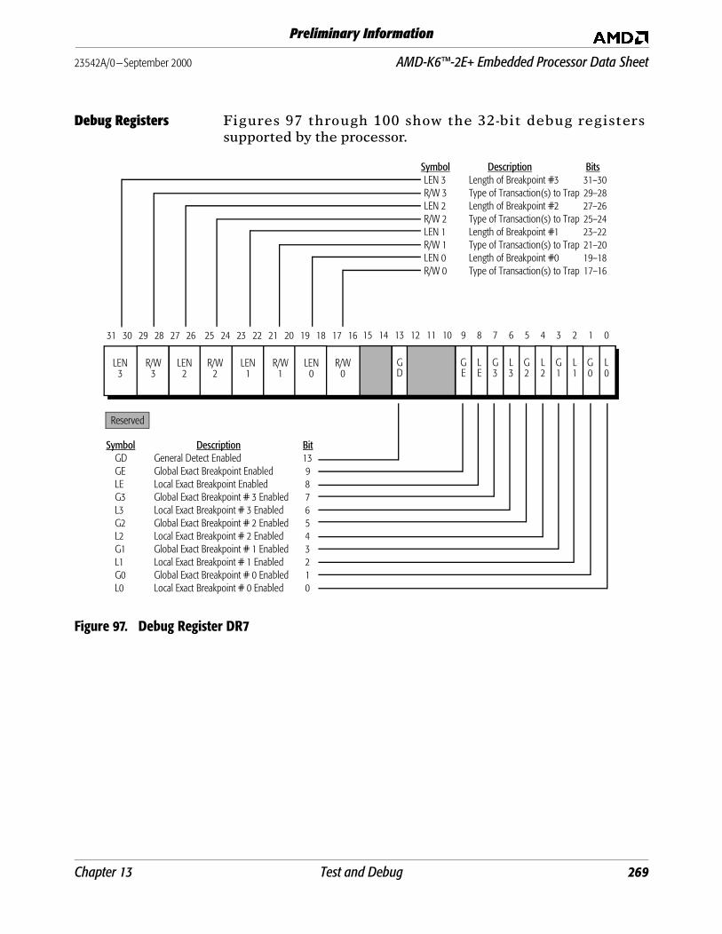
23542A/0—September 2000 AMD-K6™-2E+ Embedded Processor Data Sheet
Preliminary Information
Debug Registers Figures 97 through 100 show the 32-bit debug registerssupported by the processor.
Figure 97. Debug Register DR7
9 8 7 6 5 4 3 2 1 0101112131415
L2
L1
L3
G3
GE
LE
L0
G0
G1
G2
GD
25 24 23 22 21 20 19 18 17 16262728293031
R/W 3
LEN 3
R/W 2
LEN 2
R/W 1
LEN 1
R/W 0
LEN 0
Reserved
Symbol Description BitsLEN 3 Length of Breakpoint #3 31–30R/W 3 Type of Transaction(s) to Trap 29–28LEN 2 Length of Breakpoint #2 27–26R/W 2 Type of Transaction(s) to Trap 25–24LEN 1 Length of Breakpoint #1 23–22R/W 1 Type of Transaction(s) to Trap 21–20LEN 0 Length of Breakpoint #0 19–18R/W 0 Type of Transaction(s) to Trap 17–16
Symbol Description BitGD General Detect Enabled 13GE Global Exact Breakpoint Enabled 9LE Local Exact Breakpoint Enabled 8G3 Global Exact Breakpoint # 3 Enabled 7L3 Local Exact Breakpoint # 3 Enabled 6G2 Global Exact Breakpoint # 2 Enabled 5L2 Local Exact Breakpoint # 2 Enabled 4G1 Global Exact Breakpoint # 1 Enabled 3L1 Local Exact Breakpoint # 1 Enabled 2G0 Global Exact Breakpoint # 0 Enabled 1L0 Local Exact Breakpoint # 0 Enabled 0
Chapter 13 Test and Debug 269

AMD-K6™-2E+ Embedded Processor Data Sheet 23542A/0—September 2000
Preliminary Information
Figure 98. Debug Register DR6
Figure 99. Debug Registers DR5 and DR4
9 8 7 6 5 4 3 2 1 010111213141516171819202131 30 29 28 27 26 25 24 23 22
B1
B2
BS
B0
BT
BD
B3
Reserved
Symbol Description BitBT Breakpoint Task Switch 15 BS Breakpoint Single Step 14 BD Breakpoint Debug Access Detected 13 B3 Breakpoint #3 Condition Detected 3 B2 Breakpoint #2 Condition Detected 2 B1 Breakpoint #1 Condition Detected 1 B0 Breakpoint #0 Condition Detected 0
9 8 7 6 5 4 3 2 1 010111213141516171819202131 30 29 28 27 26 25 24 23 22
Reserved
DR5
9 8 7 6 5 4 3 2 1 010111213141516171819202131 30 29 28 27 26 25 24 23 22
Reserved
DR4
270 Test and Debug Chapter 13

23542A/0—September 2000 AMD-K6™-2E+ Embedded Processor Data Sheet
Preliminary Information
Figure 100. Debug Registers DR3, DR2, DR1, and DR0
DR3–DR0. The processor allows the setting of up to fourbreakpoints. DR3–DR0 contain the linear addresses forbreakpoint 3 through breakpoint 0, respectively, and arecompared to the linear addresses of processor cycles todetermine if a breakpoint occurs. Debug register DR7 definesthe specific type of cycle that must occur in order for thebreakpoint to occur.
DR5–DR4. When debugging extensions are disabled (bit 3 of CR4is set to 0), the DR5 and DR4 registers are mapped to DR7 andDR6, respectively, in order to be software compatible withprevious generations of x86 processors. When debugging
9 8 7 6 5 4 3 2 1 010111213141516171819202131 30 29 28 27 26 25 24 23 22
Breakpoint 3 32-bit Linear Address
DR3
9 8 7 6 5 4 3 2 1 010111213141516171819202131 30 29 28 27 26 25 24 23 22
Breakpoint 0 32-bit Linear Address
DR0
9 8 7 6 5 4 3 2 1 010111213141516171819202131 30 29 28 27 26 25 24 23 22
Breakpoint 2 32-bit Linear Address
DR2
9 8 7 6 5 4 3 2 1 010111213141516171819202131 30 29 28 27 26 25 24 23 22
Breakpoint 1 32-bit Linear Address
DR1
Chapter 13 Test and Debug 271

AMD-K6™-2E+ Embedded Processor Data Sheet 23542A/0—September 2000
Preliminary Information
extensions are enabled (bit 3 of CR4 is set to 1), any attempt toload DR5 or DR4 results in an undefined opcode exception.Likewise, any attempt to store DR5 or DR4 also results in anundefined opcode exception.
DR6. If a breakpoint is enabled in DR7, and the breakpointconditions as defined in DR7 occur, then the corresponding Bbit (B3–B0) in DR6 is set to 1. In addition, any other breakpointsdefined using these particular breakpoint conditions arereported by the processor by setting the appropriate B-bits inDR6, regardless of whether these breakpoints are enabled ordisabled. However, if a breakpoint is not enabled, a debugexception does not occur for that breakpoint.
If the processor decodes an instruction that writes or reads DR7through DR0, the BD bit (bit 13) in DR6 is set to 1 (if enabled inDR7) and the processor generates a debug exception. Thisoperation allows control to pass to the debugger prior to debugregister access by software.
If the Trap Flag (bit 8) of the EFLAGS register is set to 1, theprocessor generates a debug exception after the successfulexecution of every instruction (single-step operation) and setsthe BS bit (bit 14) in DR6 to indicate the source of theexception.
When the processor switches to a new task and the debug trapbit (T bit) in the corresponding Task State Segment (TSS) is setto 1, the processor sets the BT bit (bit 15) in DR6 and generatesa debug exception.
DR7. When set to 1, L3–L0 locally enable breakpoints 3 through0, respectively. L3–L0 are set to 0 whenever the processorexecutes a task switch. Setting L3–L0 to 0 disables thebreakpoints and ensures that these particular debug exceptionsare only generated for a specific task.
When set to 1, G3–G0 globally enable breakpoints 3 through 0,respectively. Unlike L3–L0, G3–G0 are not set to 0 whenever theprocessor executes a task switch. Not setting G3–G0 to 0 allowsbreakpoints to remain enabled across all tasks. If a breakpointis enabled globally but disabled locally, the global enableoverrides the local enable.
272 Test and Debug Chapter 13
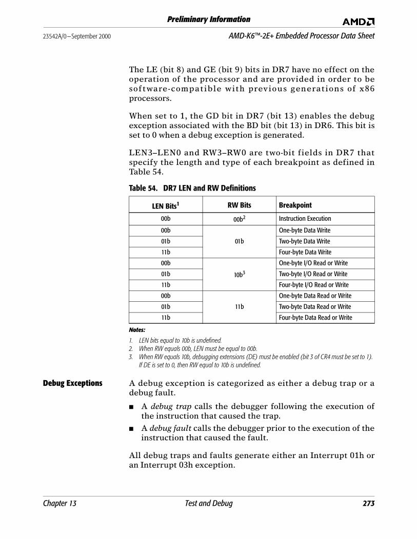
23542A/0—September 2000 AMD-K6™-2E+ Embedded Processor Data Sheet
Preliminary Information
The LE (bit 8) and GE (bit 9) bits in DR7 have no effect on theoperation of the processor and are provided in order to besoftware-compatible with previous generations of x86processors.
When set to 1, the GD bit in DR7 (bit 13) enables the debugexception associated with the BD bit (bit 13) in DR6. This bit isset to 0 when a debug exception is generated.
LEN3–LEN0 and RW3–RW0 are two-bit fields in DR7 thatspecify the length and type of each breakpoint as defined inTable 54.
Debug Exceptions A debug exception is categorized as either a debug trap or adebug fault.
■ A debug trap calls the debugger following the execution ofthe instruction that caused the trap.
■ A debug fault calls the debugger prior to the execution of theinstruction that caused the fault.
All debug traps and faults generate either an Interrupt 01h oran Interrupt 03h exception.
Table 54. DR7 LEN and RW Definitions
LEN Bits1
Notes:
1. LEN bits equal to 10b is undefined.
RW Bits Breakpoint
00b 00b2
2. When RW equals 00b, LEN must be equal to 00b.
Instruction Execution
00b
01b
One-byte Data Write
01b Two-byte Data Write
11b Four-byte Data Write
00b
10b3
3. When RW equals 10b, debugging extensions (DE) must be enabled (bit 3 of CR4 must be set to 1). If DE is set to 0, then RW equal to 10b is undefined.
One-byte I/O Read or Write
01b Two-byte I/O Read or Write
11b Four-byte I/O Read or Write
00b
11b
One-byte Data Read or Write
01b Two-byte Data Read or Write
11b Four-byte Data Read or Write
Chapter 13 Test and Debug 273
AMD-K6™-2E+ Embedded Processor Data Sheet 23542A/0—September 2000
Preliminary Information
Interrupt 01h. The following events are considered debug trapsthat cause the processor to generate an Interrupt 01hexception:
■ Enabled breakpoints for data and I/O cycles
■ Single Step Trap
■ Task Switch Trap
The following events are considered debug faults that cause theprocessor to generate an Interrupt 01h exception:
■ Enabled breakpoints for instruction execution
■ BD bit in DR6 set to 1
Interrupt 03h. The INT 3 instruction is defined in the x86architecture as a breakpoint instruction. This instructioncauses the processor to generate an Interrupt 03h exception.This exception is a debug trap because the debugger is calledfollowing the execution of the INT 3 instruction.
The INT 3 instruction is a one-byte instruction (opcode CCh)typically used to insert a breakpoint in software by writing CChto the address of the first byte of the instruction to be trapped(the target instruction). Following the trap, if the targetinstruction is to be executed, the debugger must replace theINT 3 instruction with the first byte of the target instruction.
274 Test and Debug Chapter 13
23542A/0—September 2000 AMD-K6™-2E+ Embedded Processor Data Sheet
Preliminary Information
14 Clock Control
14.1 Clock Control States
The standard-power versions of the AMD-K6-2E+ processorsupport five modes of clock control. The low-power versions ofthe AMD-K6-2E+ processor support six modes of clock control.
The processor can transition between these modes to maximizeperformance, to minimize power dissipation, or to provide abalance between performance and power. (See “PowerDissipation” on page 289 for the maximum power dissipation ofthe AMD-K6-2E+ processor within the normal andreduced-power states.) The clock-control states supported are:
■ Normal State—The processor is running in Real Mode,Virtual-8086 Mode, Protected Mode, or System ManagementMode (SMM). In this state, all clocks are running—includingthe external bus clock CLK and the internal processorclock—and the full features and functions of the processorare available.
■ Halt State—This low-power state is entered following thesuccessful execution of the HLT instruction. During thisstate, the internal processor clock is stopped.
■ Stop Grant State—This low-power state is entered followingthe recognition of the assertion of the STPCLK# signal.During this state, the internal processor clock is stopped.
■ Stop Grant Inquire State—This state is entered from theHalt state and the Stop Grant state as the result of asystem-initiated inquire cycle.
■ Enhanced Power Management (EPM) Stop Grant State: Thislow-power state is available on low--power versions of theprocessor. It is entered following the write of a non-zerovalue to the SGTC field of the EPM 16-byte I/O block for thepurpose of performing dynamic processor core frequencyand voltage ID state transitions using AMD PowerNow!technology. During this state, the internal processor clock isstopped.
■ Stop Clock State—This low-power state is entered from theStop Grant state when the CLK signal is stopped.
Chapter 14 Clock Control 275
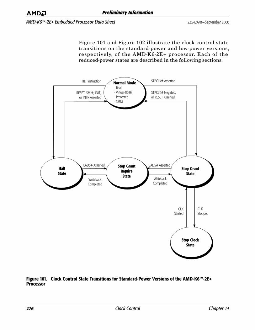
AMD-K6™-2E+ Embedded Processor Data Sheet 23542A/0—September 2000
Preliminary Information
Figure 101 and Figure 102 illustrate the clock control statetransitions on the standard-power and low-power versions,respectively, of the AMD-K6-2E+ processor. Each of thereduced-power states are described in the following sections.
Figure 101. Clock Control State Transitions for Standard-Power Versions of the AMD-K6™-2E+ Processor
EADS# Asserted EADS# Asserted
HLT Instruction
Stop GrantState
Normal Mode - Real - Virtual-8086 - Protected - SMM
HaltState
Stop ClockState
RESET, SMI#, INIT,or INTR Asserted
Stop GrantInquireState
STPCLK# Asserted
STPCLK# Negated, or RESET Asserted
CLKStarted
CLKStopped
WritebackCompleted
WritebackCompleted
276 Clock Control Chapter 14
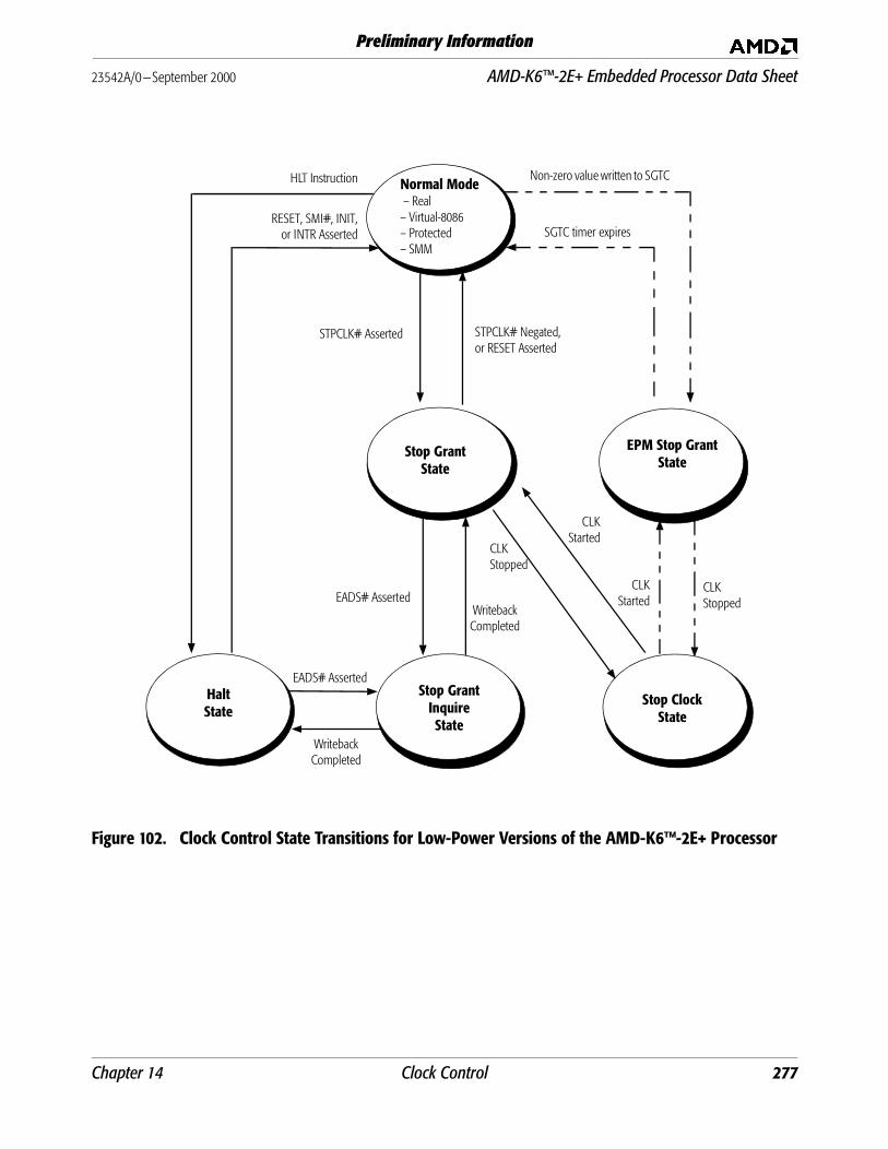
23542A/0—September 2000 AMD-K6™-2E+ Embedded Processor Data Sheet
Preliminary Information
Figure 102. Clock Control State Transitions for Low-Power Versions of the AMD-K6™-2E+ Processor
CLKStarted
CLKStopped
SGTC timer expires
Non-zero value written to SGTC
EADS# Asserted
EADS# Asserted
HLT Instruction
Stop GrantState
Normal Mode – Real– Virtual-8086– Protected– SMM
HaltState
Stop ClockState
RESET, SMI#, INIT,or INTR Asserted
Stop GrantInquireState
STPCLK# Asserted STPCLK# Negated, or RESET Asserted
CLKStarted
CLKStoppedWriteback
Completed
WritebackCompleted
EPM Stop GrantState
Chapter 14 Clock Control 277
AMD-K6™-2E+ Embedded Processor Data Sheet 23542A/0—September 2000
Preliminary Information
278 Clock Control Chapter 14
14.2 Halt State
Enter Halt State During the execution of the HLT instruction, the AMD-K6-2E+processor executes a Halt special cycle. After BRDY# issampled asserted during this cycle, and then EWBE# is alsosampled asserted (if not masked off), the processor enters theHalt state in which the processor disables most of its internalclock distribution. In order to support the following operations,the internal phase-lock loop (PLL) still runs, and some internalresources are still clocked in the Halt state:
■ Inquire Cycles—The processor continues to sample AHOLD,BOFF#, and HOLD in order to support inquire cycles thatare initiated by the system logic. The processor transitions tothe Stop Grant Inquire state during the inquire cycle. Afterreturning to the Halt state following the inquire cycle, theprocessor does not execute another Halt special cycle.
■ Flush Cycles—The processor continues to sample FLUSH#.If FLUSH# is sampled asserted, the processor performs theflush operation in the same manner as it is performed in theNormal state. Upon completing the flush operation, theprocessor executes the Halt special cycle, which indicatesthe processor is in the Halt state.
■ Time Stamp Counter (TSC)—The TSC continues to count inthe Halt state.
■ Signal Sampling—The processor continues to sample INIT,INTR, NMI, RESET, and SMI#.
After entering the Halt state, all signals driven by the processorretain their state as they existed following the completion ofthe Halt special cycle.
Exit Halt State The AMD-K6-2E+ processor remains in the Halt state until itsamples INIT, INTR (if interrupts are enabled), NMI, RESET, orSMI# asserted. If any of these signals is sampled asserted, theprocessor returns to the Normal state and performs thecorresponding operation. All of the normal requirements forrecognition of these input signals apply within the Halt state.
14.3 Stop Grant State
Enter Stop Grant State
After recognizing the assertion of STPCLK#, the AMD-K6-2E+processor flushes its instruction pipelines, completes allpending and in-progress bus cycles, and acknowledges the

23542A/0—September 2000 AMD-K6™-2E+ Embedded Processor Data Sheet
Preliminary Information
STPCLK# assertion by executing a Stop Grant special bus cycle.After BRDY# is sampled asserted during this cycle, and thenEWBE# is also sampled asserted (if not masked off), theprocessor enters the Stop Grant state.
The Stop Grant state is like the Halt state in that the processordisables most of its internal clock distribution in the Stop Grantstate.
In order to support the following operations, the internal PLLstill runs, and some internal resources are still clocked in theStop Grant state:
■ Inquire cycles—The processor transitions to the Stop GrantInquire state during an inquire cycle. After returning to theStop Grant state following the inquire cycle, the processordoes not execute another Stop Grant special cycle.
■ Time Stamp Counter (TSC)—The TSC continues to count inthe Stop Grant state.
■ Signal Sampling—The processor continues to sample INIT,INTR, NMI, RESET, and SMI#.
FLUSH# is not recognized in the Stop Grant state (unlike whilein the Halt state).
Upon entering the Stop Grant state, all signals driven by theprocessor retain their state as they existed following thecompletion of the Stop Grant special cycle.
Exit Stop Grant State The AMD-K6-2E+ processor remains in the Stop Grant stateuntil it samples STPCLK# negated or RESET asserted. IfSTPCLK# is sampled negated, the processor returns to theNormal state in less than 10 bus clock (CLK) periods. After thetransition to the Normal state, the processor resumes executionat the instruction boundary on which STPCLK# was initiallyrecognized.
If STPCLK# is recognized as negated in the Stop Grant stateand subsequently sampled asserted prior to returning to theNormal state, the AMD-K6-2E+ processor guarantees that aminimum of one instruction is executed prior to re-entering theStop Grant state.
If INIT, INTR (if interrupts are enabled), FLUSH#, NMI, orSMI# are sampled asserted in the Stop Grant state, the
Chapter 14 Clock Control 279
AMD-K6™-2E+ Embedded Processor Data Sheet 23542A/0—September 2000
Preliminary Information
processor latches the edge-sensitive signals (INIT, FLUSH#,NMI, and SMI#), but otherwise does not exit the Stop Grantstate to service the interrupt. When the processor returns to theNormal state due to sampling STPCLK# negated, any pendinginterrupts are recognized after returning to the Normal state.To ensure their recognition, all of the normal requirements forthese input signals apply within the Stop Grant state.
If RESET is sampled asserted in the Stop Grant state, theprocessor immediately returns to the Normal state and thereset process begins.
14.4 Stop Grant Inquire State
Enter Stop Grant Inquire State
The Stop Grant Inquire state is entered from the Stop Grantstate or the Halt state when EADS# is sampled asserted duringan inquire cycle initiated by the system logic. The AMD-K6-2E+processor responds to an inquire cycle in the same manner as inthe Normal state by driving HIT# and HITM#. If the inquirecycle hits a modified cache line, the processor performs awriteback cycle.
Exit Stop Grant Inquire State
Following the completion of any writeback, the processorreturns to the state from which it entered the Stop GrantInquire state.
280 Clock Control Chapter 14
23542A/0—September 2000 AMD-K6™-2E+ Embedded Processor Data Sheet
Preliminary Information
14.5 EPM Stop Grant State
Enter EPM Stop Grant State
This state is supported on the low-power versions of theAMD-K6-2E+ processor. After receiving a write of a non-zerovalue to the SGTC (Stop Grant Time-out Counter) field locatedwithin the EPM 16-byte I/O block, the processor flushes itsinstruction pipelines, completes all pending and in-progressbus cycles, and performs the following:
■ Drives the processor VID[4:0] output pins to the value storedin the VIDO field of the EPM 16-byte I/O block (see “EPM16-Byte I/O Block” on page 146) if the VIDC bit is set to 1.
■ Forwards the processor-to-bus clock ratio stored in theIBF[2:0] field of the EPM 16-byte I/O block to the internalPLL if the BDC[1:0] value is set to 1xb.
The EPM Stop Grant state is like the Halt state in that theprocessor disables most of its internal clock distribution in theEPM Stop Grant state. In order to support the followingoperations, the internal PLL still runs, and some internalresources are still clocked in the EPM Stop Grant state.
■ Time Stamp Counter (TSC): The TSC continues to count inthe EPM Stop Grant state.
■ Signal Sampling: The processor continues to sample INIT,INTR, NMI, RESET, and SMI#.
Unlike the Halt and Stop Grant states, system-initiated inquirecycles are not supported and must be prevented during theEPM Stop Grant state.
FLUSH# is not recognized in the EPM Stop Grant state (unlikewhile in the Halt state).
Upon entering the EPM Stop Grant state, all signals driven bythe processor retain their state as they existed following thecompletion of the EPM Stop Grant special cycle.
Exit EPM Stop Grant State
The processor remains in the EPM Stop Grant state until theallotted time expires, as determined by the value written to theSGTC field, or until RESET is sampled asserted. Once theallotted time expires, the processor returns to the Normal state.After the transition to the Normal state, the processor resumesexecution at the instruction boundary on which the EPM StopGrant state was entered.
Chapter 14 Clock Control 281

AMD-K6™-2E+ Embedded Processor Data Sheet 23542A/0—September 2000
Preliminary Information
If INIT, INTR (if interrupts are enabled), FLUSH#, NMI, orSMI# are sampled asserted in the EPM Stop Grant state, theprocessor latches the edge-sensitive signals (INIT, FLUSH#,NMI, and SMI#), but otherwise does not exit the EPM StopGrant state to service the interrupt. When the processor returnsto the Normal state, any pending interrupts are recognized. Toensure their recognition, all of the normal requirements forthese input signals apply within the EPM Stop Grant state.
If RESET is sampled asserted in the EPM Stop Grant state, theprocessor immediately returns to the Normal state and thereset process begins.
282 Clock Control Chapter 14
23542A/0—September 2000 AMD-K6™-2E+ Embedded Processor Data Sheet
Preliminary Information
14.6 Stop Clock State
Enter Stop Clock State
If the CLK signal is stopped while the AMD-K6-2E+ processor isin the Stop Grant state, the processor enters the Stop Clockstate. Because all internal clocks and the PLL are not runningin the Stop Clock state, the Stop Clock state represents theminimum-power state of all clock control states. The CLK signalmust be held Low while it is stopped.
The Stop Clock state cannot be entered from the Halt state.
INTR is the only input signal that is allowed to change stateswhile the processor is in the Stop Clock state. However, INTR isnot sampled until the processor returns to the Stop Grant state.All other input signals must remain unchanged in the StopClock state.
Exit Stop Clock State The AMD-K6-2E+ processor returns to the Stop Grant statefrom the Stop Clock state after the CLK signal is started andthe internal PLL has stabilized. PLL stabilization is achievedafter the CLK signal has been running within its specificationfor a minimum of 1.0 ms.
The frequency of CLK when exiting the Stop Clock state can bedifferent than the frequency of CLK when entering the StopClock state.
The state of the BF[2:0] signals when exiting the Stop Clockstate is ignored because the BF[2:0] signals are only sampledduring the falling transition of RESET.
Chapter 14 Clock Control 283

AMD-K6™-2E+ Embedded Processor Data Sheet 23542A/0—September 2000
Preliminary Information
284 Clock Control Chapter 14
23542A/0—September 2000 AMD-K6™-2E+ Embedded Processor Data Sheet
Preliminary Information
15 Electrical Data
This chapter includes specifications for the operating ranges,absolute ratings, and DC characteristics of the AMD-K6-2E+embedded processor. Nominal and maximum power dissipationvalues for the AMD-K6-2E+ processor during normal andreduced power states are listed. The chapter concludes with adiscussion of power and grounding requirements.
Chapter 15 Electrical Data 285
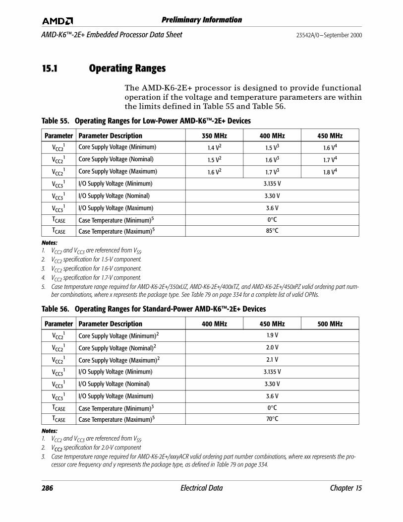
AMD-K6™-2E+ Embedded Processor Data Sheet 23542A/0—September 2000
Preliminary Information
15.1 Operating Ranges
The AMD-K6-2E+ processor is designed to provide functionaloperation if the voltage and temperature parameters are withinthe limits defined in Table 55 and Table 56.
Table 55. Operating Ranges for Low-Power AMD-K6™-2E+ Devices
Parameter Parameter Description 350 MHz 400 MHz 450 MHz
VCC21
Notes:1. VCC2 and VCC3 are referenced from VSS.
Core Supply Voltage (Minimum) 1.4 V2
2. VCC2 specification for 1.5-V component.
1.5 V3
3. VCC2 specification for 1.6-V component.
1.6 V4
4. VCC2 specification for 1.7-V component.
VCC21 Core Supply Voltage (Nominal) 1.5 V2 1.6 V3 1.7 V4
VCC21 Core Supply Voltage (Maximum) 1.6 V2 1.7 V3 1.8 V4
VCC31 I/O Supply Voltage (Minimum) 3.135 V
VCC31 I/O Supply Voltage (Nominal) 3.30 V
VCC31 I/O Supply Voltage (Maximum) 3.6 V
TCASE Case Temperature (Minimum)5
5. Case temperature range required for AMD-K6-2E+/350xUZ, AMD-K6-2E+/400xTZ, and AMD-K6-2E+/450xPZ valid ordering part num-ber combinations, where x represents the package type. See Table 79 on page 334 for a complete list of valid OPNs.
0�C
TCASE Case Temperature (Maximum)5 85�C
Table 56. Operating Ranges for Standard-Power AMD-K6™-2E+ Devices
Parameter Parameter Description 400 MHz 450 MHz 500 MHz
VCC21
Notes:1. VCC2 and VCC3 are referenced from VSS.
Core Supply Voltage (Minimum)2
2. VCC2 specification for 2.0-V component
1.9 V
VCC21 Core Supply Voltage (Nominal)2 2.0 V
VCC21 Core Supply Voltage (Maximum)2 2.1 V
VCC31 I/O Supply Voltage (Minimum) 3.135 V
VCC31 I/O Supply Voltage (Nominal) 3.30 V
VCC31 I/O Supply Voltage (Maximum) 3.6 V
TCASE Case Temperature (Minimum)3
3. Case temperature range required for AMD-K6-2E+/xxxyACR valid ordering part number combinations, where xxx represents the pro-cessor core frequency and y represents the package type, as defined in Table 79 on page 334.
0�C
TCASE Case Temperature (Maximum)5 70�C
286 Electrical Data Chapter 15
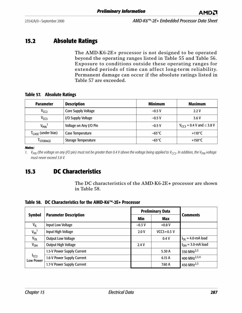
23542A/0—September 2000 AMD-K6™-2E+ Embedded Processor Data Sheet
Preliminary Information
15.2 Absolute Ratings
The AMD-K6-2E+ processor is not designed to be operatedbeyond the operating ranges listed in Table 55 and Table 56.Exposure to conditions outside these operating ranges forextended periods of time can affect long-term reliability.Permanent damage can occur if the absolute ratings listed inTable 57 are exceeded.
15.3 DC Characteristics
The DC characteristics of the AMD-K6-2E+ processor are shownin Table 58.
Table 57. Absolute Ratings
Parameter Description Minimum MaximumVCC2 Core Supply Voltage –0.5 V 2.2 V
VCC3 I/O Supply Voltage –0.5 V 3.6 V
VPIN1
Notes:1. VPIN (the voltage on any I/O pin) must not be greater than 0.4 V above the voltage being applied to VCC3. In addition, the VPIN voltage
must never exceed 3.8 V.
Voltage on Any I/O Pin –0.5 V VCC3 + 0.4 V and � 3.8 V
TCASE (under bias) Case Temperature –65�C +110�C
TSTORAGE Storage Temperature –65�C +150�C
Table 58. DC Characteristics for the AMD-K6™-2E+ Processor
Symbol Parameter DescriptionPreliminary Data
CommentsMin Max
VIL Input Low Voltage –0.3 V +0.8 V
VIH1 Input High Voltage 2.0 V VCC3+0.3 V
VOL Output Low Voltage 0.4 V IOL = 4.0-mA load
VOH Output High Voltage 2.4 V IOH = 3.0-mA load
ICC2Low Power
1.5-V Power Supply Current 5.30 A 350 MHz2,3
1.6-V Power Supply Current 6.15 A 400 MHz2,3,4
1.7-V Power Supply Current 7.60 A 450 MHz2,3
Chapter 15 Electrical Data 287
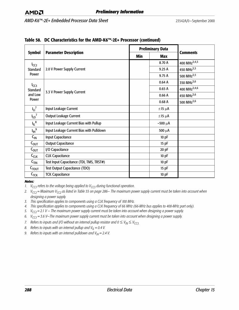
AMD-K6™-2E+ Embedded Processor Data Sheet 23542A/0—September 2000
Preliminary Information
ICC2Standard
Power2.0 V Power Supply Current
8.70 A 400 MHz3,4,5
9.25 A 450 MHz3,5
9.75 A 500 MHz3,5
ICC3Standard and Low Power
3.3 V Power Supply Current
0.64 A 350 MHz3,6
0.65 A 400 MHz3,4,6
0.66 A 450 MHz3,6
0.68 A 500 MHz3,6
ILI7 Input Leakage Current �15 mA
ILO7 Output Leakage Current �15 mA
IIL8 Input Leakage Current Bias with Pullup –500 mA
IIH9 Input Leakage Current Bias with Pulldown 500 mA
CIN Input Capacitance 10 pF
COUT Output Capacitance 15 pF
COUT I/O Capacitance 20 pF
CCLK CLK Capacitance 10 pF
CTIN Test Input Capacitance (TDI, TMS, TRST#) 10 pF
CTOUT Test Output Capacitance (TDO) 15 pF
CTCK TCK Capacitance 10 pF
Notes:1. VCC3 refers to the voltage being applied to VCC3 during functional operation.2. VCC2 = Maximum VCC2 as listed in Table 55 on page 286— The maximum power supply current must be taken into account when
designing a power supply.3. This specification applies to components using a CLK frequency of 100 MHz.4. This specification applies to components using a CLK frequency of 66 MHz (66-MHz bus applies to 400-MHz part only).5. VCC2 = 2.1 V — The maximum power supply current must be taken into account when designing a power supply.6. VCC3 = 3.6 V—The maximum power supply current must be taken into account when designing a power supply.
7. Refers to inputs and I/O without an internal pullup resistor and 0 � VIN � VCC3.8. Refers to inputs with an internal pullup and VIL = 0.4 V.9. Refers to inputs with an internal pulldown and VIH = 2.4 V.
Table 58. DC Characteristics for the AMD-K6™-2E+ Processor (continued)
Symbol Parameter DescriptionPreliminary Data
CommentsMin Max
288 Electrical Data Chapter 15
23542A/0—September 2000 AMD-K6™-2E+ Embedded Processor Data Sheet
Preliminary Information
15.4 Power Dissipation
Table 59 and Table 60 contain the application power dissipationof the low-power and standard-power AMD-K6-2E+ processorduring normal and reduced power states. Table 61 on page 290shows the supported voltages and operating frequencies forlow-power versions of AMD-K6-2E+ processors enabled withAMD PowerNow! technology.
Table 59. Power Dissipation for Low-Power AMD-K6™-2E+ Devices
Power Dissipation 350 MHz1
Notes:1. This specification applies to components using a CLK frequency of 100 MHz.
400 MHz1,2
2. This specification applies to components using a CLK frequency of 66 MHz.
450 MHz1
Application PowerActive3
3. The active application power measurements were taken by running a suite of embedded benchmarks covering four major embedded market segments: automotive, office automation, networking, and telecommunications.
5.60 W 6.90 W 8.70 W
AMD PowerNow! Technology Power Saving Mode4
4. AMD PowerNow! technology Power Saving Mode represents averaged values measured while running the processor in the lowest settings supported by AMD PowerNow! technology.
2.95 W
Thermal Design Power (Maximum)5,6
5. The maximum power dissipated in the normal clock control state must be taken into account when designing a solution for thermal dissipation for the AMD-K6-2E+ processor.
6. Maximum power is determined for the worst-case instruction sequence or function for the listed clock control states with VCC2 = Nominal VCC2 as listed in Table 55 on page 286 and VCC3 = 3.3 V.
7.50 W 9.50 W 12.00 W
Stop Grant/Halt (Maximum)6,7
7. The CLK signal and the internal PLL are still running, but most internal clocking has stopped.
VCC Nominal 2.50 W
Stop Clock (Maximum)6,8
8. The CLK signal, the internal PLL, and all internal clocking has stopped.
VCC Nominal 1.60 W 1.90 W
Lowest Operating VCC9
9. The lowest operating VCC is 1.4 V.
1.30 W
Chapter 15 Electrical Data 289
AMD-K6™-2E+ Embedded Processor Data Sheet 23542A/0—September 2000
Preliminary Information
Table 60. Power Dissipation for Standard-Power AMD-K6™-2E+ Devices
Power Dissipation 400 MHz1,2
Notes:1. This specification applies to components using a CLK frequency of 100 MHz.2. This specification applies to components using a CLK frequency of 66 MHz.
450 MHz1 500 MHz1
Application Power Active3
3. The active application power measurements were taken by running a suite of embedded benchmarks covering four major embedded market segments: automotive, office automation, networking, and telecommunications.
11.40 W 12.65 W 13.90 W
Thermal Design Power (Maximum)4,5
4. The maximum power dissipated in the normal clock control state must be taken into account when designing a solution for thermal dissipation for the AMD-K6-2E+ processor.
5. Maximum power is determined for the worst-case instruction sequence or function for the listed clock control states with VCC2 = 2.0 V and VCC3 = 3.3 V.
16.50 W 17.50 W 18.50 W
Stop Grant/Halt (Maximum)5,6
6. The CLK signal and the internal PLL are still running, but most internal clocking has stopped.
4.50 W
Stop Clock (Maximum)5,7
7. The CLK signal, the internal PLL, and all internal clocking has stopped.
4.00 W
Table 61. Supported Voltages and Operating Frequencies for Low-Power AMD-K6™-2E+ Processors Enabled with AMD PowerNow!™ Technology
Ordering Part Number1
Notes:1. An x in this column represents the package type. See Table 79, “AMD-K6™-2E+ Embedded Processor Valid Ordering Part Number Com-
binations,” on page 334.
Core VoltageRange of Supported
Operating Frequencies2
2. AMD PowerNow! technology enables the operating frequency to step down in increments corresponding to the available bus frequency multipliers. Note that 250-MHz operation is not supported due to exclusion of 2.5 bus frequency multiplier.
Active Power3
3. Active application power dissipation for highest and lowest supported frequency at specified voltage.
AMD-K6-2E+/450APZ
1.7 V 450–200 MHz 8.70–4.90 W
1.6 V 400–200 MHz 6.90–4.20 W
1.5 V 350–200 MHz 5.60–3.70 W
1.4 V 300–200 MHz 4.30–2.95 W
AMD-K6-2E+/400xTZ
1.6 V 400–200 MHz 6.90–4.20 W
1.5 V 350–200 MHz 5.60–3.70 W
1.4 V 300–200 MHz 4.30–2.95 W
AMD-K6-2E+/350xUZ1.5 V 350–200 MHz 5.60–3.70 W
1.4 V 300–200 MHz 4.30–2.95 W
290 Electrical Data Chapter 15
23542A/0—September 2000 AMD-K6™-2E+ Embedded Processor Data Sheet
Preliminary Information
15.5 Power and Grounding
Power Connections The AMD-K6-2E+ processor is a dual voltage device. Twoseparate supply voltages are required: VCC2 and VCC3.
■ VCC2 provides the core voltage for the processor.
■ VCC3 provides the I/O voltage.
See “Operating Ranges” on page 286 for the value and range ofVCC2 and VCC3.
The power and ground pins for each package are listed inTable 76 on page 325 and Table 78 on page 329. Table 74 onpage 321 lists the pin differences between the two packages.The large number of power and ground pins are provided toensure that the processor and package maintain a clean andstable power distribution network.
For proper operation and functionality, all VCC2, VCC3, and VSSpins must be connected to the appropriate planes in the circuitboard. The power planes have been arranged in a pattern tosimplify routing and minimize crosstalk on the circuit board.The isolation region between two voltage planes must be atleast 0.254mm if they are in the same layer of the circuit board.(See Figure 103 on page 292.) In order to maintain alow-impedance current sink and reference, the ground planemust never be split.
Although the AMD-K6-2E+ processor has two separate supplyvoltages, there are no special power sequencing requirements.The best procedure is to minimize the time between which VCC2and VCC3 are either both on or both off.
Chapter 15 Electrical Data 291
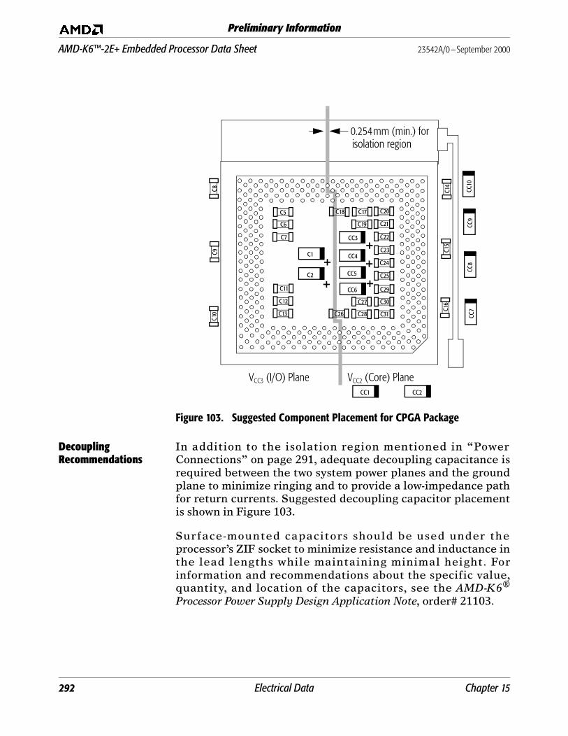
AMD-K6™-2E+ Embedded Processor Data Sheet 23542A/0—September 2000
Preliminary Information
Figure 103. Suggested Component Placement for CPGA Package
Decoupling Recommendations
In addition to the isolation region mentioned in “PowerConnections” on page 291, adequate decoupling capacitance isrequired between the two system power planes and the groundplane to minimize ringing and to provide a low-impedance pathfor return currents. Suggested decoupling capacitor placementis shown in Figure 103.
Surface-mounted capacitors should be used under theprocessor’s ZIF socket to minimize resistance and inductance inthe lead lengths while maintaining minimal height. Forinformation and recommendations about the specific value,quantity, and location of the capacitors, see the AMD-K6®
Processor Power Supply Design Application Note, order# 21103.
0.254mm (min.) for isolation region
VCC2 (Core) PlaneVCC3 (I/O) Plane
C1
CC5
CC3
C2
+
++
+
C5
C6
C7
C11
C12
C13
C17C18
C19
C20
C21
C22
C23
C24
C25
C26
C27
C28
C29
C30
C31
CC4
+
CC6
CC10
CC1 CC2
CC9
CC8
CC7
C8C9
C10
C14
C15
C16
292 Electrical Data Chapter 15

23542A/0—September 2000 AMD-K6™-2E+ Embedded Processor Data Sheet
Preliminary Information
Pin Connection Requirements
For proper operation, the following requirements for signal pinconnections must be met:
■ Do not drive address and data signals into large capacitiveloads at high frequencies. If necessary, use buffer chips todrive large capacitive loads.
■ Leave all NC (no-connect) pins unconnected.
■ Unused inputs should always be connected to anappropriate signal level.
• Active Low inputs that are not being used should beconnected to VCC3 through a 20-kW pullup resistor.
• Active High inputs that are not being used should beconnected to GND through a pulldown resistor.
■ Reserved signals can be treated in one of the following ways:
• As no-connect (NC) pins, in which case these pins are leftunconnected
• As pins connected to the system logic as defined by theindustry-standard Super7 and Socket 7 interface
• Any combination of NC and Socket 7 pins
■ Keep trace lengths to a minimum.
Chapter 15 Electrical Data 293
AMD-K6™-2E+ Embedded Processor Data Sheet 23542A/0—September 2000
Preliminary Information
294 Electrical Data Chapter 15

23542A/0—September 2000 AMD-K6™-2E+ Embedded Processor Data Sheet
Preliminary Information
16 Signal Switching Characteristics
The AMD-K6-2E+ processor signal switching characteristics arepresented in Table 62 through Table 71 on the following pages.Valid delay, float, setup, and hold timing specifications arelisted. These specifications are provided for the systemdesigner to determine if the timings necessary for the processorto interface with the system logic are met.
■ Table 62 on page 296 and Table 63 on page 297 contain theswitching characteristics of the CLK input.
■ Table 64 on page 298 through Table 67 on page 304 containthe timings for the normal operation signals.
■ Table 68 on page 306 and Table 69 on page 307 contain thetimings for RESET and the configuration signals.
■ Table 70 on page 308 and Table 71 on page 308 contain thetimings for the test operation signals.
All signal timings provided are:
■ Measured between CLK, TCK, or RESET at 1.5 V and thecorresponding signal at 1.5 V—this applies to input andoutput signals that are switching from Low to High, or fromHigh to Low
■ Based on input signals applied at a slew rate of 1 V/nsbetween 0 V and 3 V (rising) and 3 V to 0 V (falling)
■ Valid within the operating ranges given in “OperatingRanges” on page 286
■ Based on a load capacitance (CL) of 0 pF
Chapter 16 Signal Switching Characteristics 295
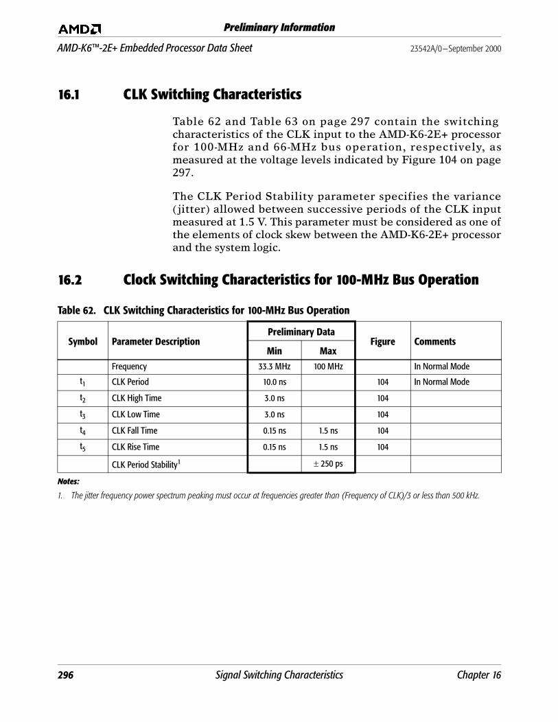
AMD-K6™-2E+ Embedded Processor Data Sheet 23542A/0—September 2000
Preliminary Information
16.1 CLK Switching Characteristics
Table 62 and Table 63 on page 297 contain the switchingcharacteristics of the CLK input to the AMD-K6-2E+ processorfor 100-MHz and 66-MHz bus operation, respectively, asmeasured at the voltage levels indicated by Figure 104 on page297.
The CLK Period Stability parameter specifies the variance(jitter) allowed between successive periods of the CLK inputmeasured at 1.5 V. This parameter must be considered as one ofthe elements of clock skew between the AMD-K6-2E+ processorand the system logic.
16.2 Clock Switching Characteristics for 100-MHz Bus Operation
Table 62. CLK Switching Characteristics for 100-MHz Bus Operation
Symbol Parameter DescriptionPreliminary Data
Figure CommentsMin Max
Frequency 33.3 MHz 100 MHz In Normal Mode
t1 CLK Period 10.0 ns 104 In Normal Mode
t2 CLK High Time 3.0 ns 104
t3 CLK Low Time 3.0 ns 104
t4 CLK Fall Time 0.15 ns 1.5 ns 104
t5 CLK Rise Time 0.15 ns 1.5 ns 104
CLK Period Stability1
Notes:
1. The jitter frequency power spectrum peaking must occur at frequencies greater than (Frequency of CLK)/3 or less than 500 kHz.
� 250 ps
296 Signal Switching Characteristics Chapter 16
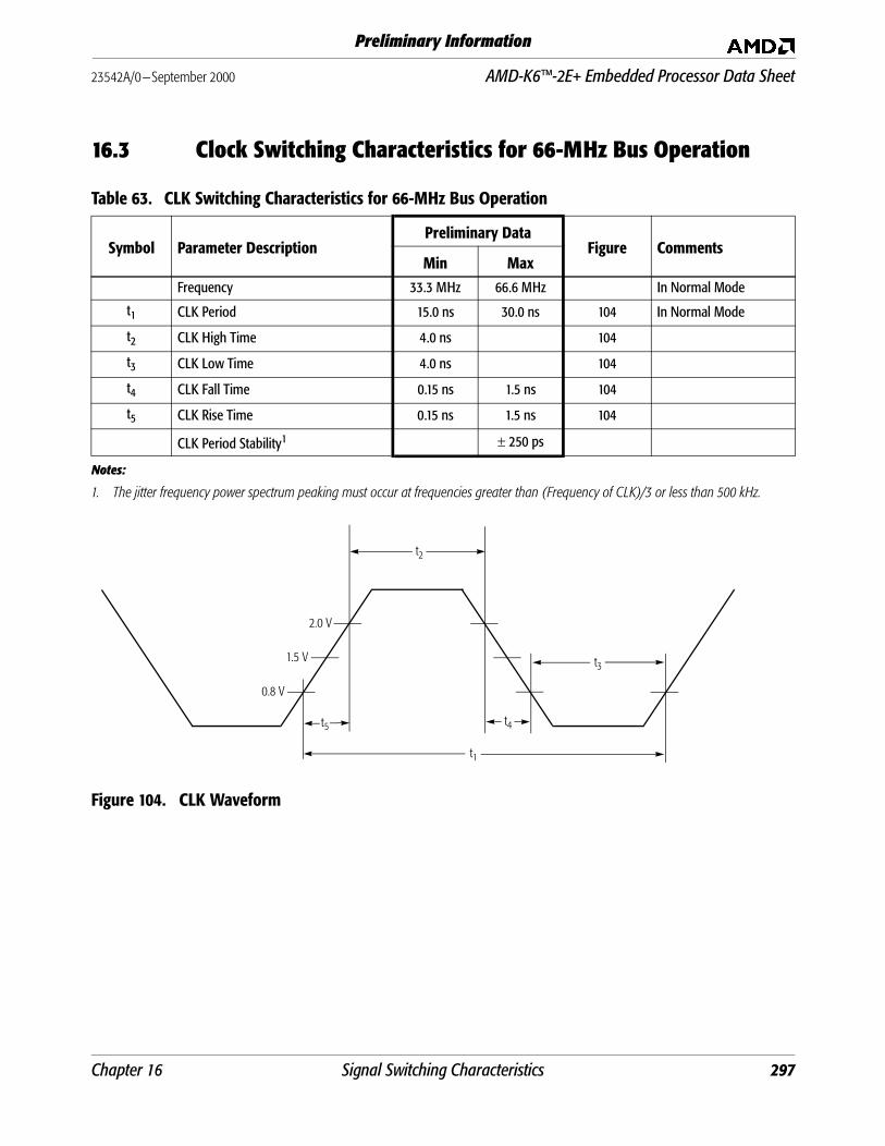
23542A/0—September 2000 AMD-K6™-2E+ Embedded Processor Data Sheet
Preliminary Information
16.3 Clock Switching Characteristics for 66-MHz Bus Operation
Figure 104. CLK Waveform
Table 63. CLK Switching Characteristics for 66-MHz Bus Operation
Symbol Parameter DescriptionPreliminary Data
Figure CommentsMin Max
Frequency 33.3 MHz 66.6 MHz In Normal Mode
t1 CLK Period 15.0 ns 30.0 ns 104 In Normal Mode
t2 CLK High Time 4.0 ns 104
t3 CLK Low Time 4.0 ns 104
t4 CLK Fall Time 0.15 ns 1.5 ns 104
t5 CLK Rise Time 0.15 ns 1.5 ns 104
CLK Period Stability1
Notes:
1. The jitter frequency power spectrum peaking must occur at frequencies greater than (Frequency of CLK)/3 or less than 500 kHz.
� 250 ps
t5
2.0 V
1.5 V
0.8 V
t2
t3
t4
t1
Chapter 16 Signal Switching Characteristics 297
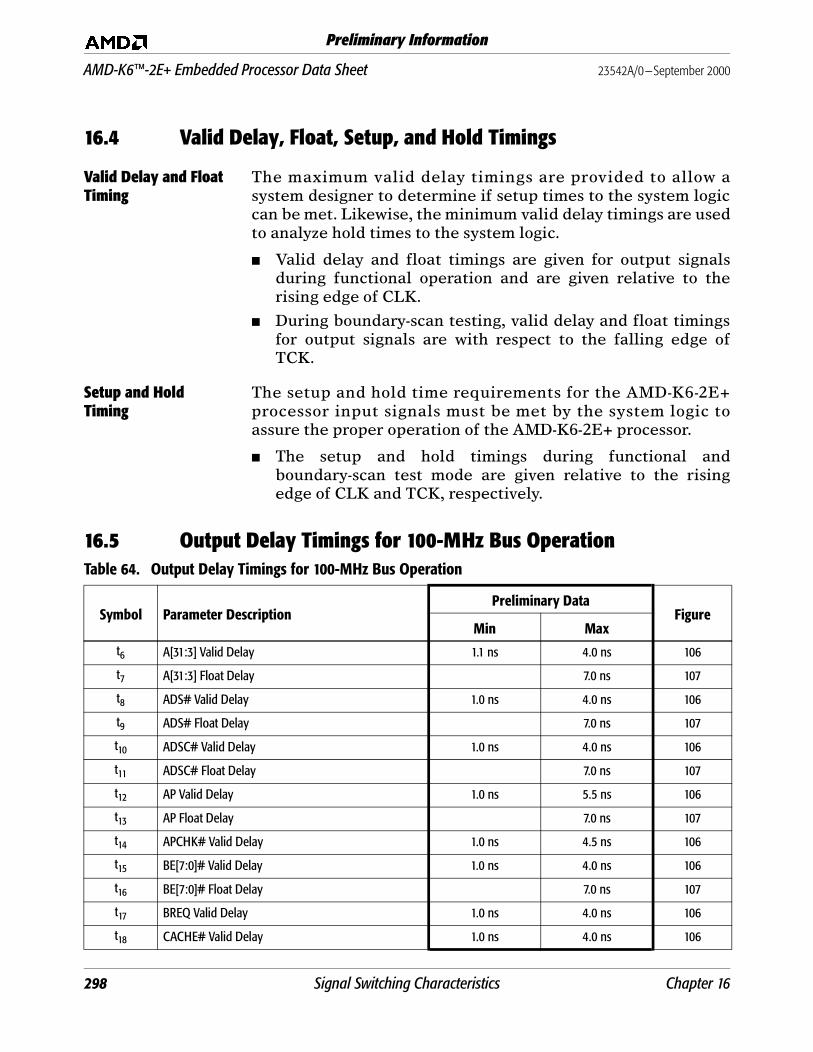
AMD-K6™-2E+ Embedded Processor Data Sheet 23542A/0—September 2000
Preliminary Information
16.4 Valid Delay, Float, Setup, and Hold Timings
Valid Delay and Float Timing
The maximum valid delay timings are provided to allow asystem designer to determine if setup times to the system logiccan be met. Likewise, the minimum valid delay timings are usedto analyze hold times to the system logic.
■ Valid delay and float timings are given for output signalsduring functional operation and are given relative to therising edge of CLK.
■ During boundary-scan testing, valid delay and float timingsfor output signals are with respect to the falling edge ofTCK.
Setup and Hold Timing
The setup and hold time requirements for the AMD-K6-2E+processor input signals must be met by the system logic toassure the proper operation of the AMD-K6-2E+ processor.
■ The setup and hold timings during functional andboundary-scan test mode are given relative to the risingedge of CLK and TCK, respectively.
16.5 Output Delay Timings for 100-MHz Bus OperationTable 64. Output Delay Timings for 100-MHz Bus Operation
Symbol Parameter DescriptionPreliminary Data
FigureMin Max
t6 A[31:3] Valid Delay 1.1 ns 4.0 ns 106
t7 A[31:3] Float Delay 7.0 ns 107
t8 ADS# Valid Delay 1.0 ns 4.0 ns 106
t9 ADS# Float Delay 7.0 ns 107
t10 ADSC# Valid Delay 1.0 ns 4.0 ns 106
t11 ADSC# Float Delay 7.0 ns 107
t12 AP Valid Delay 1.0 ns 5.5 ns 106
t13 AP Float Delay 7.0 ns 107
t14 APCHK# Valid Delay 1.0 ns 4.5 ns 106
t15 BE[7:0]# Valid Delay 1.0 ns 4.0 ns 106
t16 BE[7:0]# Float Delay 7.0 ns 107
t17 BREQ Valid Delay 1.0 ns 4.0 ns 106
t18 CACHE# Valid Delay 1.0 ns 4.0 ns 106
298 Signal Switching Characteristics Chapter 16

23542A/0—September 2000 AMD-K6™-2E+ Embedded Processor Data Sheet
Preliminary Information
t19 CACHE# Float Delay 7.0 ns 107
t20 D/C# Valid Delay 1.0 ns 4.0 ns 106
t21 D/C# Float Delay 7.0 ns 107
t22 D[63:0] Write Data Valid Delay 1.3 ns 4.5 ns 106
t23 D[63:0] Write Data Float Delay 7.0 ns 107
t24 DP[7:0] Write Data Valid Delay 1.3 ns 4.5 ns 106
t25 DP[7:0] Write Data Float Delay 7.0 ns 107
t26 FERR# Valid Delay 1.0 ns 4.5 ns 106
t27 HIT# Valid Delay 1.0 ns 4.0 ns 106
t28 HITM# Valid Delay 1.1 ns 4.0 ns 106
t29 HLDA Valid Delay 1.0 ns 4.0 ns 106
t30 LOCK# Valid Delay 1.1 ns 4.0 ns 106
t31 LOCK# Float Delay 7.0 ns 107
t32 M/IO# Valid Delay 1.0 ns 4.0 ns 106
t33 M/IO# Float Delay 7.0 ns 107
t34 PCD Valid Delay 1.0 ns 4.0 ns 106
t35 PCD Float Delay 7.0 ns 107
t36 PCHK# Valid Delay 1.0 ns 4.5 ns 106
t37 PWT Valid Delay 1.0 ns 4.0 ns 106
t38 PWT Float Delay 7.0 ns 107
t39 SCYC Valid Delay 1.0 ns 4.0 ns 106
t40 SCYC Float Delay 7.0 ns 107
t41 SMIACT# Valid Delay 1.0 ns 4.0 ns 106
t42 W/R# Valid Delay 1.0 ns 4.0 ns 106
t43 W/R# Float Delay 7.0 ns 107
Table 64. Output Delay Timings for 100-MHz Bus Operation (continued)
Symbol Parameter DescriptionPreliminary Data
FigureMin Max
Chapter 16 Signal Switching Characteristics 299
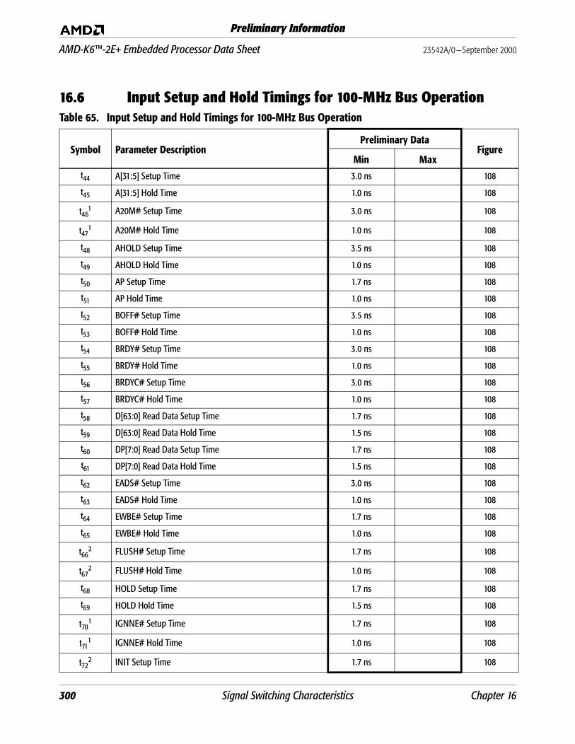
AMD-K6™-2E+ Embedded Processor Data Sheet 23542A/0—September 2000
Preliminary Information
16.6 Input Setup and Hold Timings for 100-MHz Bus OperationTable 65. Input Setup and Hold Timings for 100-MHz Bus Operation
Symbol Parameter DescriptionPreliminary Data
FigureMin Max
t44 A[31:5] Setup Time 3.0 ns 108
t45 A[31:5] Hold Time 1.0 ns 108
t461 A20M# Setup Time 3.0 ns 108
t471 A20M# Hold Time 1.0 ns 108
t48 AHOLD Setup Time 3.5 ns 108
t49 AHOLD Hold Time 1.0 ns 108
t50 AP Setup Time 1.7 ns 108
t51 AP Hold Time 1.0 ns 108
t52 BOFF# Setup Time 3.5 ns 108
t53 BOFF# Hold Time 1.0 ns 108
t54 BRDY# Setup Time 3.0 ns 108
t55 BRDY# Hold Time 1.0 ns 108
t56 BRDYC# Setup Time 3.0 ns 108
t57 BRDYC# Hold Time 1.0 ns 108
t58 D[63:0] Read Data Setup Time 1.7 ns 108
t59 D[63:0] Read Data Hold Time 1.5 ns 108
t60 DP[7:0] Read Data Setup Time 1.7 ns 108
t61 DP[7:0] Read Data Hold Time 1.5 ns 108
t62 EADS# Setup Time 3.0 ns 108
t63 EADS# Hold Time 1.0 ns 108
t64 EWBE# Setup Time 1.7 ns 108
t65 EWBE# Hold Time 1.0 ns 108
t662 FLUSH# Setup Time 1.7 ns 108
t672 FLUSH# Hold Time 1.0 ns 108
t68 HOLD Setup Time 1.7 ns 108
t69 HOLD Hold Time 1.5 ns 108
t701 IGNNE# Setup Time 1.7 ns 108
t711 IGNNE# Hold Time 1.0 ns 108
t722 INIT Setup Time 1.7 ns 108
300 Signal Switching Characteristics Chapter 16

23542A/0—September 2000 AMD-K6™-2E+ Embedded Processor Data Sheet
Preliminary Information
t732 INIT Hold Time 1.0 ns 108
t741 INTR Setup Time 1.7 ns 108
t751 INTR Hold Time 1.0 ns 108
t76 INV Setup Time 1.7 ns 108
t77 INV Hold Time 1.0 ns 108
t78 KEN# Setup Time 3.0 ns 108
t79 KEN# Hold Time 1.0 ns 108
t80 NA# Setup Time 1.7 ns 108
t81 NA# Hold Time 1.0 ns 108
t822 NMI Setup Time 1.7 ns 108
t832 NMI Hold Time 1.0 ns 108
t842 SMI# Setup Time 1.7 ns 108
t852 SMI# Hold Time 1.0 ns 108
t861 STPCLK# Setup Time 1.7 ns 108
t871 STPCLK# Hold Time 1.0 ns 108
t88 WB/WT# Setup Time 1.7 ns 108
t89 WB/WT# Hold Time 1.0 ns 108
Notes:
1. These level-sensitive signals can be asserted synchronously or asynchronously. To be sampled on a specific clock edge, setup and hold times must be met. If asserted asynchronously, they must be asserted for a minimum pulse width of two clocks.
2. These edge-sensitive signals can be asserted synchronously or asynchronously. To be sampled on a specific clock edge, setup and hold times must be met. If asserted asynchronously, they must have been negated at least two clocks prior to assertion and must remain asserted at least two clocks.
Table 65. Input Setup and Hold Timings for 100-MHz Bus Operation (continued)
Symbol Parameter DescriptionPreliminary Data
FigureMin Max
Chapter 16 Signal Switching Characteristics 301
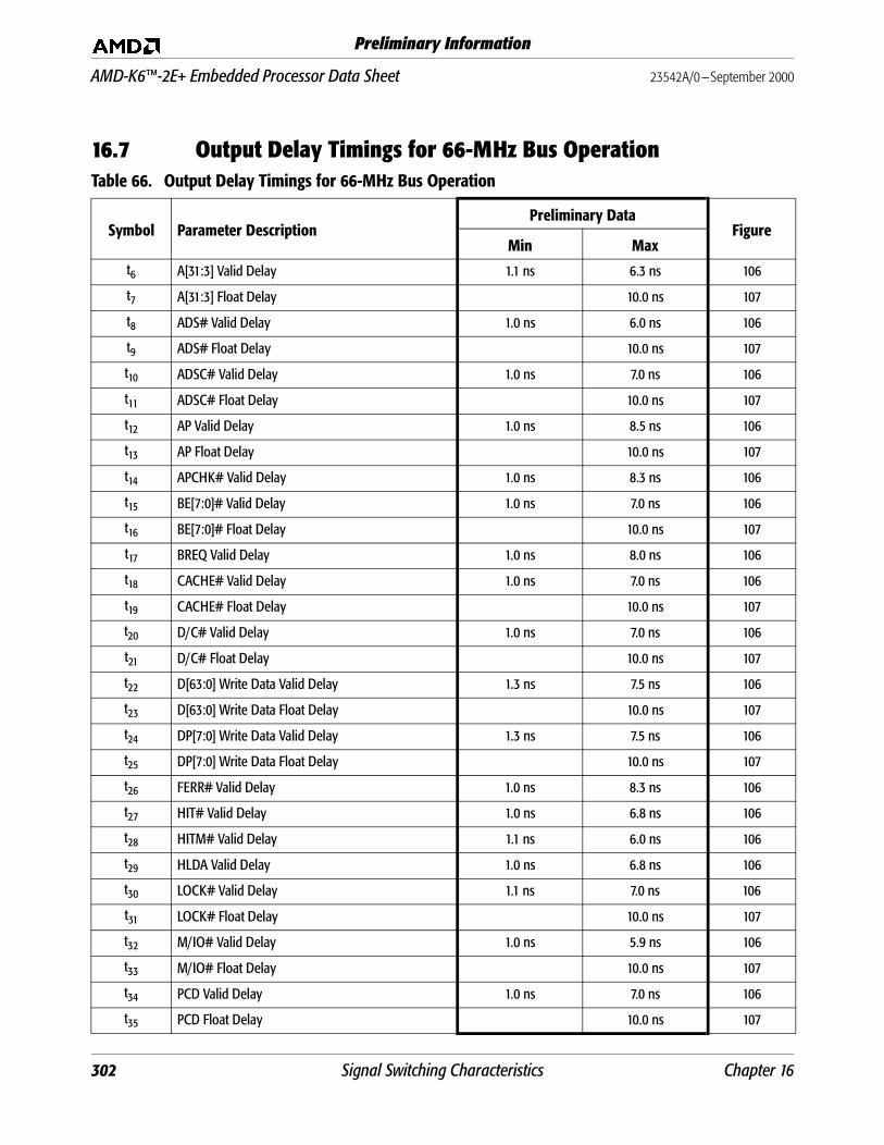
AMD-K6™-2E+ Embedded Processor Data Sheet 23542A/0—September 2000
Preliminary Information
16.7 Output Delay Timings for 66-MHz Bus OperationTable 66. Output Delay Timings for 66-MHz Bus Operation
Symbol Parameter DescriptionPreliminary Data
FigureMin Max
t6 A[31:3] Valid Delay 1.1 ns 6.3 ns 106
t7 A[31:3] Float Delay 10.0 ns 107
t8 ADS# Valid Delay 1.0 ns 6.0 ns 106
t9 ADS# Float Delay 10.0 ns 107
t10 ADSC# Valid Delay 1.0 ns 7.0 ns 106
t11 ADSC# Float Delay 10.0 ns 107
t12 AP Valid Delay 1.0 ns 8.5 ns 106
t13 AP Float Delay 10.0 ns 107
t14 APCHK# Valid Delay 1.0 ns 8.3 ns 106
t15 BE[7:0]# Valid Delay 1.0 ns 7.0 ns 106
t16 BE[7:0]# Float Delay 10.0 ns 107
t17 BREQ Valid Delay 1.0 ns 8.0 ns 106
t18 CACHE# Valid Delay 1.0 ns 7.0 ns 106
t19 CACHE# Float Delay 10.0 ns 107
t20 D/C# Valid Delay 1.0 ns 7.0 ns 106
t21 D/C# Float Delay 10.0 ns 107
t22 D[63:0] Write Data Valid Delay 1.3 ns 7.5 ns 106
t23 D[63:0] Write Data Float Delay 10.0 ns 107
t24 DP[7:0] Write Data Valid Delay 1.3 ns 7.5 ns 106
t25 DP[7:0] Write Data Float Delay 10.0 ns 107
t26 FERR# Valid Delay 1.0 ns 8.3 ns 106
t27 HIT# Valid Delay 1.0 ns 6.8 ns 106
t28 HITM# Valid Delay 1.1 ns 6.0 ns 106
t29 HLDA Valid Delay 1.0 ns 6.8 ns 106
t30 LOCK# Valid Delay 1.1 ns 7.0 ns 106
t31 LOCK# Float Delay 10.0 ns 107
t32 M/IO# Valid Delay 1.0 ns 5.9 ns 106
t33 M/IO# Float Delay 10.0 ns 107
t34 PCD Valid Delay 1.0 ns 7.0 ns 106
t35 PCD Float Delay 10.0 ns 107
302 Signal Switching Characteristics Chapter 16
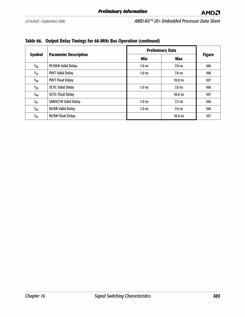
23542A/0—September 2000 AMD-K6™-2E+ Embedded Processor Data Sheet
Preliminary Information
t36 PCHK# Valid Delay 1.0 ns 7.0 ns 106
t37 PWT Valid Delay 1.0 ns 7.0 ns 106
t38 PWT Float Delay 10.0 ns 107
t39 SCYC Valid Delay 1.0 ns 7.0 ns 106
t40 SCYC Float Delay 10.0 ns 107
t41 SMIACT# Valid Delay 1.0 ns 7.3 ns 106
t42 W/R# Valid Delay 1.0 ns 7.0 ns 106
t43 W/R# Float Delay 10.0 ns 107
Table 66. Output Delay Timings for 66-MHz Bus Operation (continued)
Symbol Parameter DescriptionPreliminary Data
FigureMin Max
Chapter 16 Signal Switching Characteristics 303

AMD-K6™-2E+ Embedded Processor Data Sheet 23542A/0—September 2000
Preliminary Information
16.8 Input Setup and Hold Timings for 66-MHz Bus OperationTable 67. Input Setup and Hold Timings for 66-MHz Bus Operation
Symbol Parameter DescriptionPreliminary Data
FigureMin Max
t44 A[31:5] Setup Time 6.0 ns 108
t45 A[31:5] Hold Time 1.0 ns 108
t461 A20M# Setup Time 5.0 ns 108
t471 A20M# Hold Time 1.0 ns 108
t48 AHOLD Setup Time 5.5 ns 108
t49 AHOLD Hold Time 1.0 ns 108
t50 AP Setup Time 5.0 ns 108
t51 AP Hold Time 1.0 ns 108
t52 BOFF# Setup Time 5.5 ns 108
t53 BOFF# Hold Time 1.0 ns 108
t54 BRDY# Setup Time 5.0 ns 108
t55 BRDY# Hold Time 1.0 ns 108
t56 BRDYC# Setup Time 5.0 ns 108
t57 BRDYC# Hold Time 1.0 ns 108
t58 D[63:0] Read Data Setup Time 2.8 ns 108
t59 D[63:0] Read Data Hold Time 1.5 ns 108
t60 DP[7:0] Read Data Setup Time 2.8 ns 108
t61 DP[7:0] Read Data Hold Time 1.5 ns 108
t62 EADS# Setup Time 5.0 ns 108
t63 EADS# Hold Time 1.0 ns 108
t64 EWBE# Setup Time 5.0 ns 108
t65 EWBE# Hold Time 1.0 ns 108
t662 FLUSH# Setup Time 5.0 ns 108
t672 FLUSH# Hold Time 1.0 ns 108
t68 HOLD Setup Time 5.0 ns 108
t69 HOLD Hold Time 1.5 ns 108
t701 IGNNE# Setup Time 5.0 ns 108
t711 IGNNE# Hold Time 1.0 ns 108
t722 INIT Setup Time 5.0 ns 108
304 Signal Switching Characteristics Chapter 16
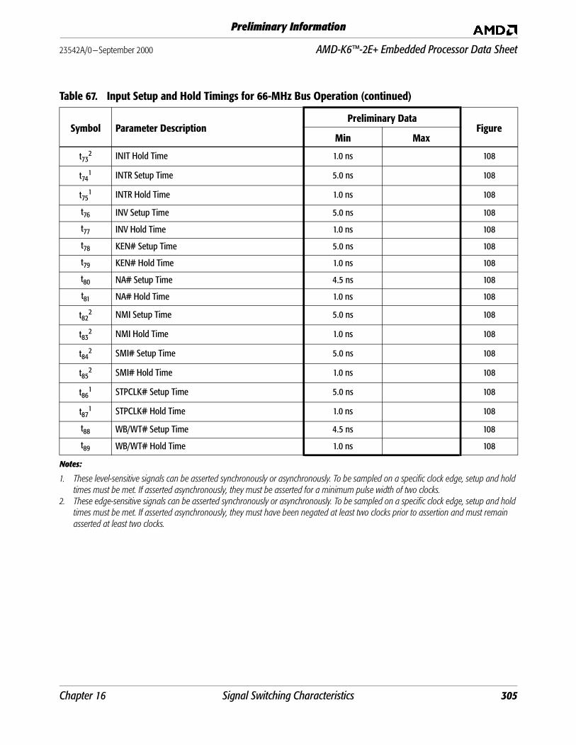
23542A/0—September 2000 AMD-K6™-2E+ Embedded Processor Data Sheet
Preliminary Information
t732 INIT Hold Time 1.0 ns 108
t741 INTR Setup Time 5.0 ns 108
t751 INTR Hold Time 1.0 ns 108
t76 INV Setup Time 5.0 ns 108
t77 INV Hold Time 1.0 ns 108
t78 KEN# Setup Time 5.0 ns 108
t79 KEN# Hold Time 1.0 ns 108
t80 NA# Setup Time 4.5 ns 108
t81 NA# Hold Time 1.0 ns 108
t822 NMI Setup Time 5.0 ns 108
t832 NMI Hold Time 1.0 ns 108
t842 SMI# Setup Time 5.0 ns 108
t852 SMI# Hold Time 1.0 ns 108
t861 STPCLK# Setup Time 5.0 ns 108
t871 STPCLK# Hold Time 1.0 ns 108
t88 WB/WT# Setup Time 4.5 ns 108
t89 WB/WT# Hold Time 1.0 ns 108
Notes:
1. These level-sensitive signals can be asserted synchronously or asynchronously. To be sampled on a specific clock edge, setup and hold times must be met. If asserted asynchronously, they must be asserted for a minimum pulse width of two clocks.
2. These edge-sensitive signals can be asserted synchronously or asynchronously. To be sampled on a specific clock edge, setup and hold times must be met. If asserted asynchronously, they must have been negated at least two clocks prior to assertion and must remain asserted at least two clocks.
Table 67. Input Setup and Hold Timings for 66-MHz Bus Operation (continued)
Symbol Parameter DescriptionPreliminary Data
FigureMin Max
Chapter 16 Signal Switching Characteristics 305
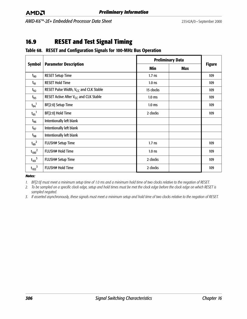
AMD-K6™-2E+ Embedded Processor Data Sheet 23542A/0—September 2000
Preliminary Information
16.9 RESET and Test Signal TimingTable 68. RESET and Configuration Signals for 100-MHz Bus Operation
Symbol Parameter DescriptionPreliminary Data
FigureMin Max
t90 RESET Setup Time 1.7 ns 109
t91 RESET Hold Time 1.0 ns 109
t92 RESET Pulse Width, VCC and CLK Stable 15 clocks 109
t93 RESET Active After VCC and CLK Stable 1.0 ms 109
t941
Notes:
1. BF[2:0] must meet a minimum setup time of 1.0 ms and a minimum hold time of two clocks relative to the negation of RESET.
BF[2:0] Setup Time 1.0 ms 109
t951 BF[2:0] Hold Time 2 clocks 109
t96 Intentionally left blank
t97 Intentionally left blank
t98 Intentionally left blank
t992
2. To be sampled on a specific clock edge, setup and hold times must be met the clock edge before the clock edge on which RESET is sampled negated.
FLUSH# Setup Time 1.7 ns 109
t1002 FLUSH# Hold Time 1.0 ns 109
t1013
3. If asserted asynchronously, these signals must meet a minimum setup and hold time of two clocks relative to the negation of RESET.
FLUSH# Setup Time 2 clocks 109
t1023 FLUSH# Hold Time 2 clocks 109
306 Signal Switching Characteristics Chapter 16

23542A/0—September 2000 AMD-K6™-2E+ Embedded Processor Data Sheet
Preliminary Information
Table 69. RESET and Configuration Signals for 66-MHz Bus Operation
Symbol Parameter DescriptionPreliminary Data
FigureMin Max
t90 RESET Setup Time 5.0 ns 109
t91 RESET Hold Time 1.0 ns 109
t92 RESET Pulse Width, VCC and CLK Stable 15 clocks 109
t93 RESET Active After VCC and CLK Stable 1.0 ms 109
t941 BF[2:0] Setup Time 1.0 ms 109
t951 BF[2:0] Hold Time 2 clocks 109
t96 Intentionally left blank
t97 Intentionally left blank
t98 Intentionally left blank
t992 FLUSH# Setup Time 5.0 ns 109
t1002 FLUSH# Hold Time 1.0 ns 109
t1013 FLUSH# Setup Time 2 clocks 109
t1023 FLUSH# Hold Time 2 clocks 109
Notes:
1. BF[2:0] must meet a minimum setup time of 1.0 ms and a minimum hold time of two clocks relative to the negation of RESET.2. To be sampled on a specific clock edge, setup and hold times must be met the clock edge before the clock edge on which RESET is sam-
pled negated.3. If asserted asynchronously, these signals must meet a minimum setup and hold time of two clocks relative to the negation of RESET.
Chapter 16 Signal Switching Characteristics 307
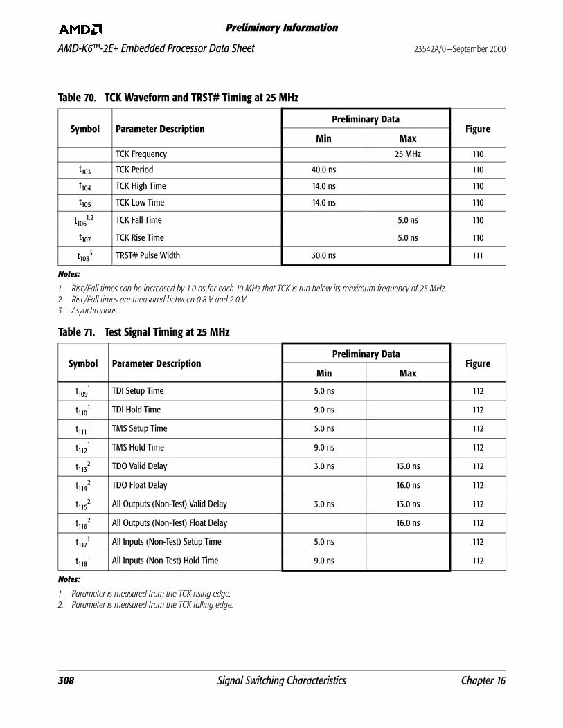
AMD-K6™-2E+ Embedded Processor Data Sheet 23542A/0—September 2000
Preliminary Information
Table 70. TCK Waveform and TRST# Timing at 25 MHz
Symbol Parameter DescriptionPreliminary Data
FigureMin Max
TCK Frequency 25 MHz 110
t103 TCK Period 40.0 ns 110
t104 TCK High Time 14.0 ns 110
t105 TCK Low Time 14.0 ns 110
t1061,2
Notes:
1. Rise/Fall times can be increased by 1.0 ns for each 10 MHz that TCK is run below its maximum frequency of 25 MHz.2. Rise/Fall times are measured between 0.8 V and 2.0 V.
TCK Fall Time 5.0 ns 110
t107 TCK Rise Time 5.0 ns 110
t1083
3. Asynchronous.
TRST# Pulse Width 30.0 ns 111
Table 71. Test Signal Timing at 25 MHz
Symbol Parameter DescriptionPreliminary Data
FigureMin Max
t1091
Notes:
1. Parameter is measured from the TCK rising edge.
TDI Setup Time 5.0 ns 112
t1101 TDI Hold Time 9.0 ns 112
t1111 TMS Setup Time 5.0 ns 112
t1121 TMS Hold Time 9.0 ns 112
t1132
2. Parameter is measured from the TCK falling edge.
TDO Valid Delay 3.0 ns 13.0 ns 112
t1142 TDO Float Delay 16.0 ns 112
t1152 All Outputs (Non-Test) Valid Delay 3.0 ns 13.0 ns 112
t1162 All Outputs (Non-Test) Float Delay 16.0 ns 112
t1171 All Inputs (Non-Test) Setup Time 5.0 ns 112
t1181 All Inputs (Non-Test) Hold Time 9.0 ns 112
308 Signal Switching Characteristics Chapter 16
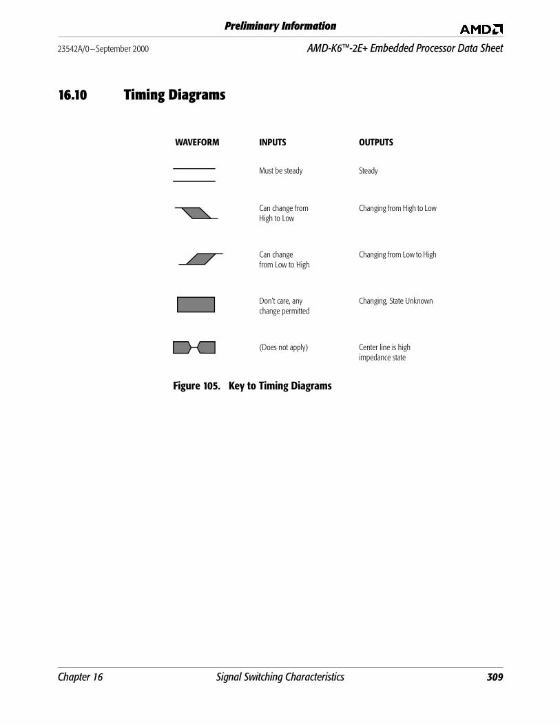
23542A/0—September 2000 AMD-K6™-2E+ Embedded Processor Data Sheet
Preliminary Information
16.10 Timing Diagrams
Figure 105. Key to Timing Diagrams
Must be steady
Can change from High to Low
Can changefrom Low to High
(Does not apply)
Don’t care, anychange permitted
Steady
Changing from High to Low
Changing from Low to High
Changing, State Unknown
Center line is high impedance state
WAVEFORM INPUTS OUTPUTS
Chapter 16 Signal Switching Characteristics 309
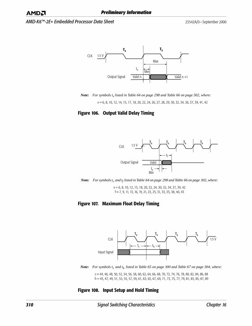
AMD-K6™-2E+ Embedded Processor Data Sheet 23542A/0—September 2000
Preliminary Information
Figure 106. Output Valid Delay Timing
Figure 107. Maximum Float Delay Timing
Figure 108. Input Setup and Hold Timing
Min
Max
Valid n +1
tv
Valid n
CLK
Output Signal
TxTx
1.5 V
Note: For symbols tv listed in Table 64 on page 298 and Table 66 on page 302, where:
v = 6, 8, 10, 12, 14, 15, 17, 18, 20, 22, 24, 26, 27, 28, 29, 30, 32, 34, 36, 37, 39, 41, 42
Tx Tx Tx
Valid
Tx
tvMin
Output Signal
tf
CLK 1.5 V
Note: For symbols tv and tf listed in Table 64 on page 298 and Table 66 on page 302, where:
v = 6, 8, 10, 12, 15, 18, 20, 22, 24, 30, 32, 34, 37, 39, 42f = 7, 9, 11, 13, 16, 19, 21, 23, 25, 31, 33, 35, 38, 40, 43
CLK
Tx Tx Tx Tx
Input Signal
ts th
1.5 V
Note: For symbols ts and th listed in Table 65 on page 300 and Table 67 on page 304, where:
s = 44, 46, 48, 50, 52, 54, 56, 58, 60, 62, 64, 66, 68, 70, 72, 74, 76, 78, 80, 82, 84, 86, 88h = 45, 47, 49, 51, 53, 55, 57, 59, 61, 63, 65, 67, 69, 71, 73, 75, 77, 79, 81, 83, 85, 87, 89
310 Signal Switching Characteristics Chapter 16
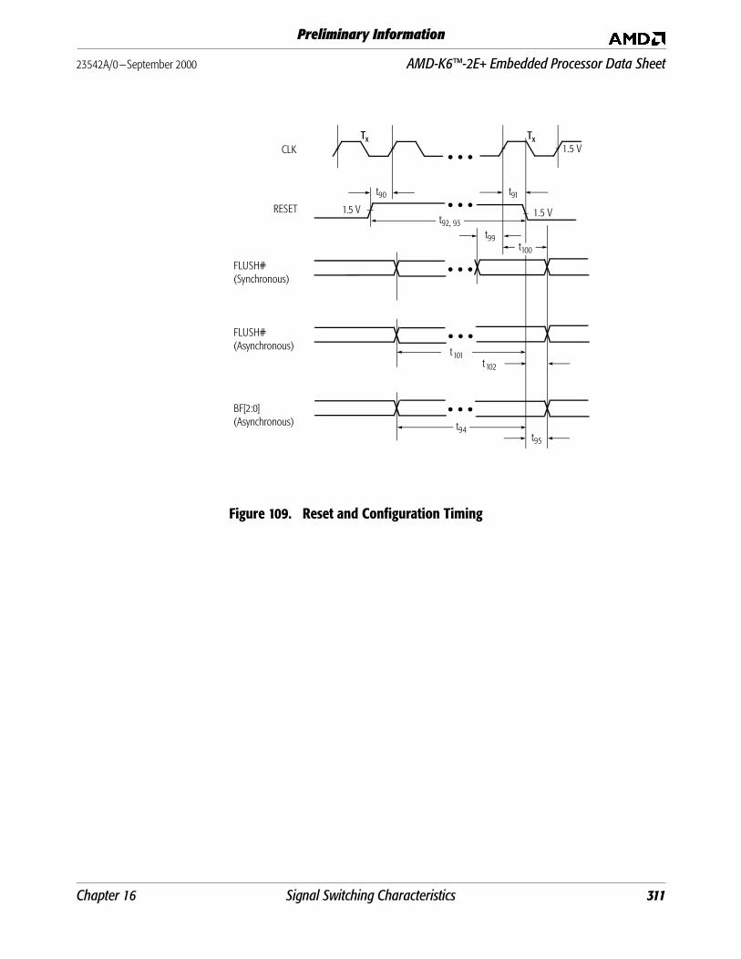
23542A/0—September 2000 AMD-K6™-2E+ Embedded Processor Data Sheet
Preliminary Information
Figure 109. Reset and Configuration Timing
TxCLK
RESET
Tx
t90
FLUSH#(Synchronous)
1.5 V
1.5 V1.5 V • • •t92, 93
t91
t99t100
• • •
BF[2:0](Asynchronous) t94
• • •
t95
FLUSH#(Asynchronous) t101
t102
• • •
• • •
Chapter 16 Signal Switching Characteristics 311
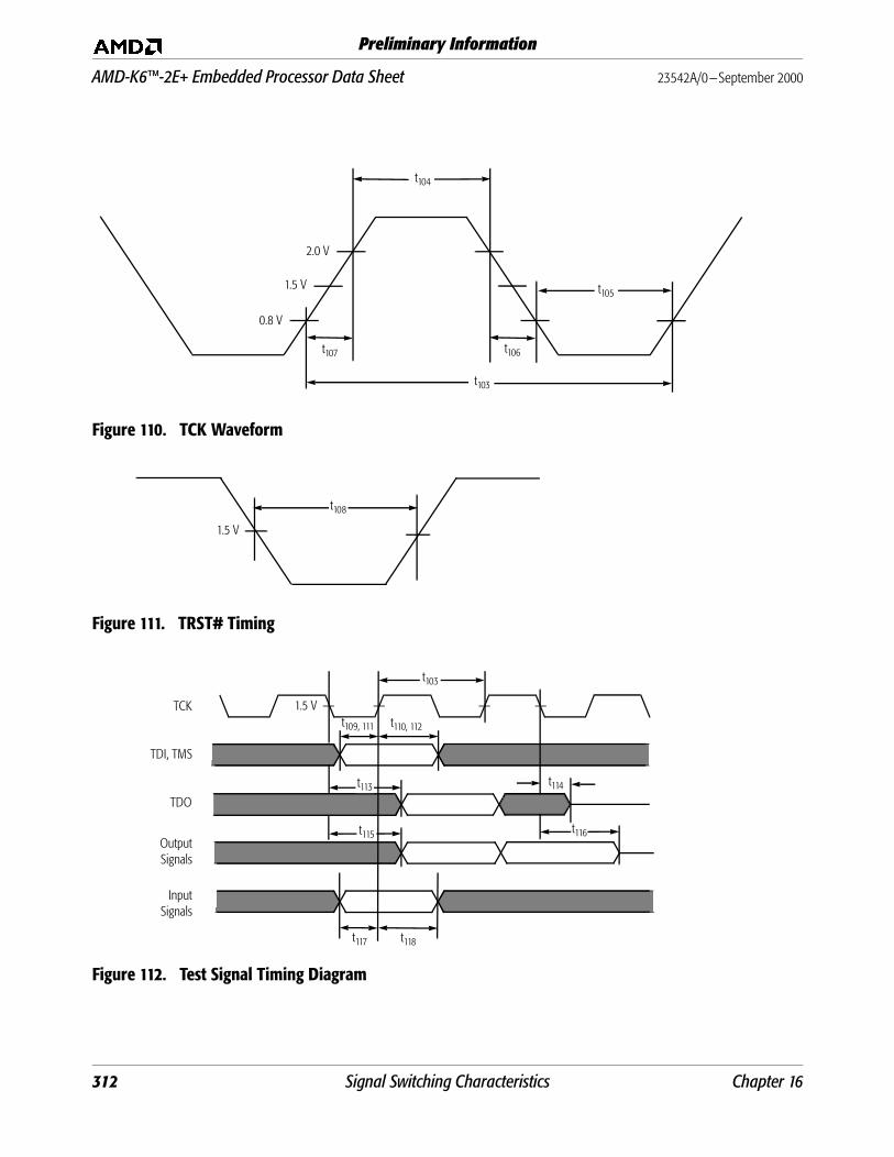
AMD-K6™-2E+ Embedded Processor Data Sheet 23542A/0—September 2000
Preliminary Information
Figure 110. TCK Waveform
Figure 111. TRST# Timing
Figure 112. Test Signal Timing Diagram
t107
2.0 V
1.5 V
0.8 V
t105
t106
t103
t104
1.5 V
t108
TCK
TDI, TMS
TDO
OutputSignals
InputSignals
t103
t109, 111 t110, 112
t113
t115 t116
t117 t118
t114
1.5 V
312 Signal Switching Characteristics Chapter 16
23542A/0—September 2000 AMD-K6™-2E+ Embedded Processor Data Sheet
Preliminary Information
17 Thermal Design
17.1 Package Thermal Specifications
The AMD-K6-2E+ processor operating specification calls for thecase temperature (TC) to be in the range of 0°C to 70°C forstandard-power devices and 0°C to 85°C for low-power devices.The ambient temperature (TA) is not specified as long as thecase temperature is not violated. The case temperature must bemeasured on the top center of the package.
Table 72 on page 314 and Table 73 on page 314 show the pro-cessor thermal specifications for the low-power and standard power AMD-K6-2E+ devices, respectively.
Chapter 17 Thermal Design 313
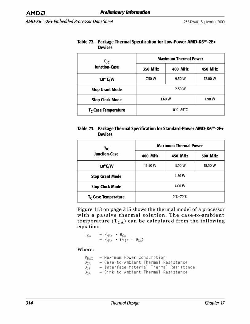
AMD-K6™-2E+ Embedded Processor Data Sheet 23542A/0—September 2000
Preliminary Information
Figure 113 on page 315 shows the thermal model of a processorwith a passive thermal solution. The case-to-ambienttemperature (TCA) can be calculated from the followingequation:
TCA = PMAX • qCA= PMAX • ( qIF + qSA)
Where:
PMAX = Maximum Power ConsumptionqCA = Case-to-Ambient Thermal ResistanceqIF = Interface Material Thermal ResistanceqSA = Sink-to-Ambient Thermal Resistance
Table 72. Package Thermal Specification for Low-Power AMD-K6™-2E+ Devices
qJCJunction-Case
Maximum Thermal Power
350 MHz 400 MHz 450 MHz
1.0° C/W 7.50 W 9.50 W 12.00 W
Stop Grant Mode 2.50 W
Stop Clock Mode 1.60 W 1.90 W
TC Case Temperature 0°C–85°C
Table 73. Package Thermal Specification for Standard-Power AMD-K6™-2E+ Devices
qJCJunction-Case
Maximum Thermal Power
400 MHz 450 MHz 500 MHz
1.0°C/W 16.50 W 17.50 W 18.50 W
Stop Grant Mode 4.50 W
Stop Clock Mode 4.00 W
TC Case Temperature 0°C–70°C
314 Thermal Design Chapter 17
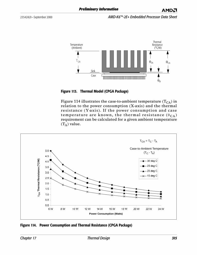
23542A/0—September 2000 AMD-K6™-2E+ Embedded Processor Data Sheet
Preliminary Information
Figure 113. Thermal Model (CPGA Package)
Figure 114 illustrates the case-to-ambient temperature (TCA) inrelation to the power consumption (X-axis) and the thermalresistance (Y-axis). If the power consumption and casetemperature are known, the thermal resistance (qCA)requirement can be calculated for a given ambient temperature(TA) value.
Figure 114. Power Consumption and Thermal Resistance (CPGA Package)
TemperatureThermal
qSA qCA
qIF
(°C/W)(Ambient)
Case
Sink
TCA
Resistance
���
���
���
���
���
���
���
���
���
���
���
��: ��: ���: ���: ���: ���: ���: ���: ���: ���:
Power Consumption (Watts)
���GHJ�&
���GHJ�&
���GHJ�&
���GHJ�&
Case-to-Ambient Temperature(TC - TA)
q
CA T
her
mal
Res
ista
nce
(°C
/W)
TCA = TC - TA
Chapter 17 Thermal Design 315
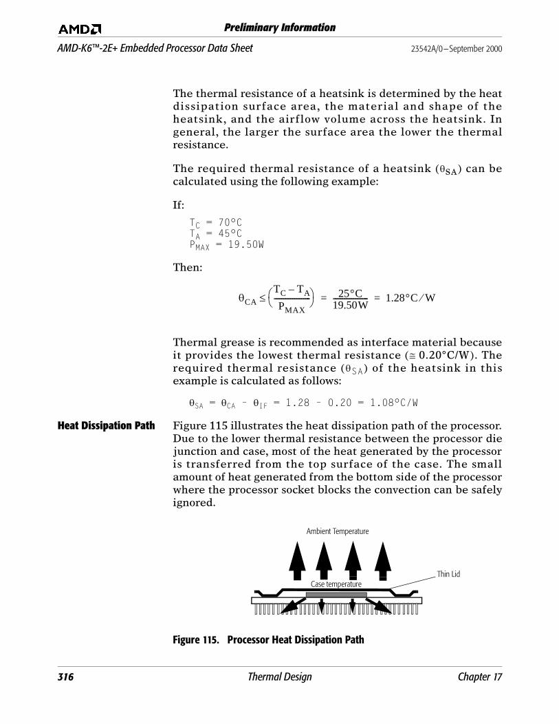
AMD-K6™-2E+ Embedded Processor Data Sheet 23542A/0—September 2000
Preliminary Information
The thermal resistance of a heatsink is determined by the heatdissipation surface area, the material and shape of theheatsink, and the airflow volume across the heatsink. Ingeneral, the larger the surface area the lower the thermalresistance.
The required thermal resistance of a heatsink (qSA) can becalculated using the following example:
If:
TC = 70°CTA = 45°CPMAX = 19.50W
Then:
Thermal grease is recommended as interface material becauseit provides the lowest thermal resistance (@ 0.20°C/W). Therequired thermal resistance (qSA) of the heatsink in thisexample is calculated as follows:
qSA = qCA – qIF = 1.28 – 0.20 = 1.08°C/W
Heat Dissipation Path Figure 115 illustrates the heat dissipation path of the processor.Due to the lower thermal resistance between the processor diejunction and case, most of the heat generated by the processoris transferred from the top surface of the case. The smallamount of heat generated from the bottom side of the processorwhere the processor socket blocks the convection can be safelyignored.
Figure 115. Processor Heat Dissipation Path
qCA
TC TA–
PMAX--------------------Í Ý
Ë Û� 25�C19.50W------------------- 1.28�C W�= =
Thin LidCase temperature
Ambient Temperature
316 Thermal Design Chapter 17
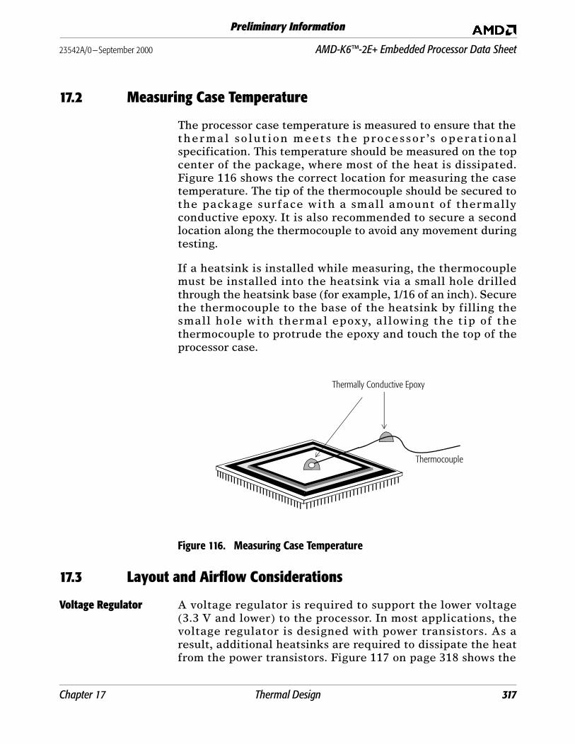
23542A/0—September 2000 AMD-K6™-2E+ Embedded Processor Data Sheet
Preliminary Information
17.2 Measuring Case Temperature
The processor case temperature is measured to ensure that thethermal so lut ion meets the processor ’s operat ionalspecification. This temperature should be measured on the topcenter of the package, where most of the heat is dissipated.Figure 116 shows the correct location for measuring the casetemperature. The tip of the thermocouple should be secured tothe package surface with a small amount of thermallyconductive epoxy. It is also recommended to secure a secondlocation along the thermocouple to avoid any movement duringtesting.
If a heatsink is installed while measuring, the thermocouplemust be installed into the heatsink via a small hole drilledthrough the heatsink base (for example, 1/16 of an inch). Securethe thermocouple to the base of the heatsink by filling thesmall hole with thermal epoxy, allowing the tip of thethermocouple to protrude the epoxy and touch the top of theprocessor case.
Figure 116. Measuring Case Temperature
17.3 Layout and Airflow Considerations
Voltage Regulator A voltage regulator is required to support the lower voltage(3.3 V and lower) to the processor. In most applications, thevoltage regulator is designed with power transistors. As aresult, additional heatsinks are required to dissipate the heatfrom the power transistors. Figure 117 on page 318 shows the
Thermocouple
Thermally Conductive Epoxy
Chapter 17 Thermal Design 317
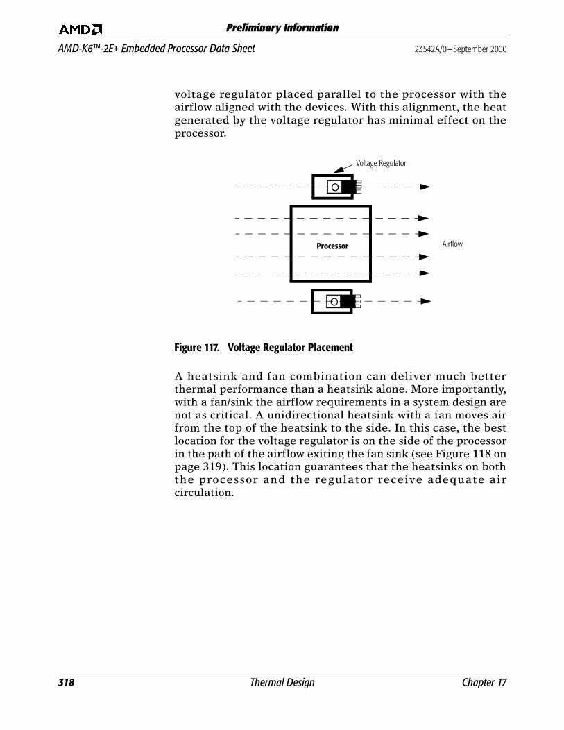
AMD-K6™-2E+ Embedded Processor Data Sheet 23542A/0—September 2000
Preliminary Information
voltage regulator placed parallel to the processor with theairflow aligned with the devices. With this alignment, the heatgenerated by the voltage regulator has minimal effect on theprocessor.
Figure 117. Voltage Regulator Placement
A heatsink and fan combination can deliver much betterthermal performance than a heatsink alone. More importantly,with a fan/sink the airflow requirements in a system design arenot as critical. A unidirectional heatsink with a fan moves airfrom the top of the heatsink to the side. In this case, the bestlocation for the voltage regulator is on the side of the processorin the path of the airflow exiting the fan sink (see Figure 118 onpage 319). This location guarantees that the heatsinks on boththe processor and the regulator receive adequate aircirculation.
Processor Airflow
Voltage Regulator
318 Thermal Design Chapter 17
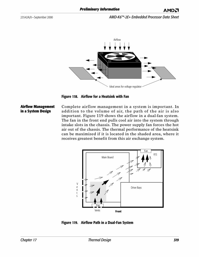
23542A/0—September 2000 AMD-K6™-2E+ Embedded Processor Data Sheet
Preliminary Information
Figure 118. Airflow for a Heatsink with Fan
Airflow Management in a System Design
Complete airflow management in a system is important. Inaddition to the volume of air, the path of the air is alsoimportant. Figure 119 shows the airflow in a dual-fan system.The fan in the front end pulls cool air into the system throughintake slots in the chassis. The power supply fan forces the hotair out of the chassis. The thermal performance of the heatsinkcan be maximized if it is located in the shaded area, where itreceives greatest benefit from this air exchange system.
Figure 119. Airflow Path in a Dual-Fan System
Airflow
Ideal areas for voltage regulator
Drive Bays
P/S
Vents
Vents
Fan
Fan
Main Board
Front
Chapter 17 Thermal Design 319
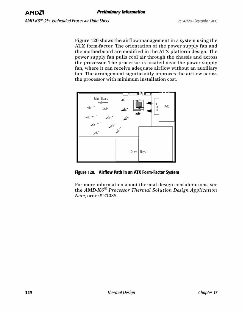
AMD-K6™-2E+ Embedded Processor Data Sheet 23542A/0—September 2000
Preliminary Information
Figure 120 shows the airflow management in a system using theATX form-factor. The orientation of the power supply fan andthe motherboard are modified in the ATX platform design. Thepower supply fan pulls cool air through the chassis and acrossthe processor. The processor is located near the power supplyfan, where it can receive adequate airflow without an auxiliaryfan. The arrangement significantly improves the airflow acrossthe processor with minimum installation cost.
Figure 120. Airflow Path in an ATX Form-Factor System
For more information about thermal design considerations, seethe AMD-K6® Processor Thermal Solution Design ApplicationNote, order# 21085.
P/S
Main Board
Drive Bays
Fan
320 Thermal Design Chapter 17

23542A/0—September 2000 AMD-K6™-2E+ Embedded Processor Data Sheet
Preliminary Information
Chapter 18 Pin Designations 321
18 Pin DesignationsThis chapter includes pin connection diagrams and pindesignation tables for each of two packages, the Ceramic PinGrid Array (CPGA) and the Organic Ball Grid Array (OBGA).
The pin designat ion diagrams include the followingannotations:
Note that the OBGA package includes additional pins notsupported on the CPGA package. Table 74 shows the pindifferences between the two packages.
Control/Parity Pins Address Pins
VSS Pins T Test Pins
VCC2 Pins NC, INC (Internal No Connect) Pins
VCC3 Pins RSVD (Reserved) Pins
Data Pins
Table 74. Pin Differences Between the CPGA and OBGA Packages
Pin CPGA Package OGBA Package Comment
VCC2DET Supported Not supported
VCC2H/L# Supported Not supported
VID[4:0]Supported on low-power versions only
Supported on low-power versions only
These pins are no-connects (NC) on standard-power versions for both packages.
VCC2 28 37
VCC3 32 26
VSS 68 99
No Connects131
82
Notes:1. Standard-power versions only, since the VID[4:0] outputs are not supported.2. Low-power versions only.
131
82
Internal No Connects
7 1
Reserved 14 16
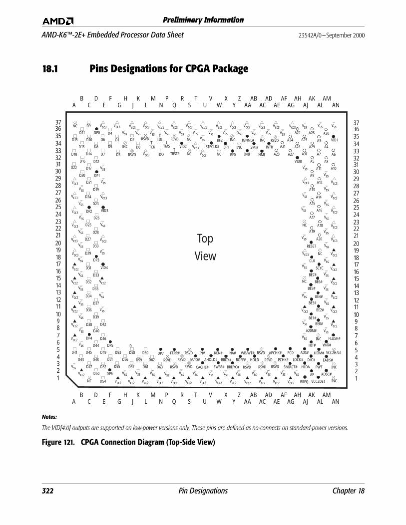
AMD-K6™-2E+ Embedded Processor Data Sheet 23542A/0—September 2000
Preliminary Information
18.1 Pins Designations for CPGA Package
Notes:
The VID[4:0] outputs are supported on low-power versions only. These pins are defined as no-connects on standard-power versions.
Figure 121. CPGA Connection Diagram (Top-Side View)
A8
RSVDRSVDRSVD
RSVD
BF2
BF1
BF0TDO
A28 A30
A10
A20
BE7#
BE6#
BE5#
BE4#
BE3#
BE2#
BE1#
A20M#
ADS#
LOCK#
PCD
BE0#
D/C#
PWT
APCHK#
EADS#
HLDA
BRDY#
BRDYC#
ADSC#
EWBE#
BOFF# HOLD
RSVD
RSVD
RSVD
RSVD
RSVD
RSVDRSVD RSVD
AP
M/IO# PCHK#AHOLD#RSVD
RSVD
D0
D2D1
D3
TDI
D4
D5
D7
D12
D19
D21
DP1
D17
D20
D22
D18 D14
D15 D10
D16
D13
DP0
D9
D11
D6
D24
D23
DP2
D25
D8
D26
D28
D27
D30
D29
DP3
D31
D33
D32
D35
D34
D37
D39
D42
D40
D36
D38
DP4
D45
D44 DP5
D46
D53 D60 DP7
D43
D41 D49
D51
D58
D59 D62
D61 D63D57D55
D50
D47
D56
DP6
D54
D52
D48
A6
A26 A29
BREQ VCC2DET
VCC2H/L#WB/WT#
30
28
20
18
10
8
TopView
Data Pins
16
9
19
6
26
29
36
Vcc2
Vcc3
Vss
FERR#
D
Vcc3
Vcc3Vcc3Vcc3Vcc3Vcc3Vcc3Vcc3Vcc3
Vcc3
Vcc3
Vcc3
Vcc3
Vcc3
Vcc3
Vcc3
Vcc3
Vcc3
Vcc3
Vcc3
Vcc3Vcc3Vcc3Vcc3
A23 A27
A21
INIT
SMI#
NMI
INC
NC
STPCLK#
VID0
INC
IGNNE#
TRST#
TMS
INC
NC
A22
A25A24
A31 A7
A3
A4
A5
A9
A13
A14
A15
A11
A12
A16
A17
A19
INTR
RESET
CLK
SCYC
NC
NC
INC FLUSH#
HIT#
INV KEN# NA#
CACHE# SMIACT#
HITM#
W/R#
INC
INC
INC
NC
VssVssVssVssVssVss
Vss
Vss
VssVss
Vss
VssVssVssVssVssVss
Vss
Vss
Vss
Vss
Vss
Vss
Vss
Vss
Vss
Vss
Vss
Vss
Vss
Vss
Vss
A18
Vss
Vss
Vss
Vss
Vss
Vss Vss Vss Vss Vss
Vss
Vss
Vss
Vss Vss Vss Vss Vss Vss VssVss
Vss
Vss
Vss
Vss
Vss
Vss
Vss
Vss
Vss
Vss
VssVss
Vss
Vcc2
Vcc2Vcc2
Vcc2
Vcc2
Vcc2
Vcc2
Vcc2
Vcc2
Vcc2Vcc2 Vcc2Vcc2Vcc2Vcc2Vcc2
Vcc2
Vcc2
Vcc2
Vcc2 Vcc2
Vcc2
Vcc2Vcc2Vcc2Vcc2
Vss
Vcc2
TCK
Vcc3
Vcc3
Vcc3
Vcc3
Vcc3Vcc3
Vcc3
37
3534333231
27
2524232221
17
14131211
15
7
54321
30
28
20
18
10
8
16
9
19
6
26
29
3637
3534333231
27
2524232221
17
14131211
15
7
54321
QA C E G J L N S WU Y AA AC AE AG AJ AL ANB D P AB ADF H K M R T V X Z AF AH AK AM
QA C E G J L N S WU Y AA AC AE AG AJ AL ANB D P AB ADF H K M R T V X Z AF AH AK AM
VID2
NC
NC VID1
VID3
VID4
NC
322 Pin Designations Chapter 18
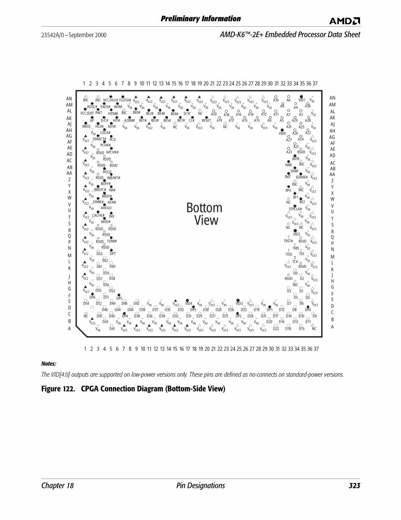
23542A/0—September 2000 AMD-K6™-2E+ Embedded Processor Data Sheet
Preliminary Information
Notes:
The VID[4:0] outputs are supported on low-power versions only. These pins are defined as no-connects on standard-power versions.
Figure 122. CPGA Connection Diagram (Bottom-Side View)
BottomView
HOLD
HLDA ADS#BREQ
APCHK#
LOCK#
PCHK#PCD
D/C#
PWT
AP BE1#
BE2#
BE3# BE5#
BE0# BE4# BE6#
RSVD
RSVD
RSVD
RSVD RSVD
BE7#
RSVD
RSVD
ADSC# EADS#
BRDY#
BRDYC#
BOFF#
EWBE#
RSVD
RSVDRSVD
AHOLD
M/IO#
FERR#
WB/WT#
KEN#
SMIACT#
A20M# RESET
A20
A19 A17A18
A15
HITM#VCC2DET
D63 DP7
D61
D57D59
D58
D55 D53
D62D60
D56
DP5D51DP6
D54
D44
D42
D39 D33
D52 D49
D40 D35 DP3D37
D46
D47 D45 DP4
D48
D43
D41
D38 D36 D34 D32 D31 D27D29 D25 DP2
D30 D28 D26 D23
RSVD
RSVD
RSVD
D19 DP1 D12
D24 D21 D17
D3
D5
DP0
D6
D14D11
D15
D7
D10 D9D20
D22
D13D16
D18
D4
D2D0
TDO TDI
D1
D8
TCK
TMS
TRST#
BF0
BF1BF2
STPCLK#
IGNNE#
INTR
SMI#
NMI
INIT
INC
A26
VID1
INC
INC
INC VCC2H/L#INC FLUSH#
INC
NC
A9
A16
A6
A30
A29 A28
A10ANAMALAKAJ
AHAGAFAEADACABAAZYXWVUTSRQPNMLK
JHGFEDCBA
ANAMALAKAJAHAGAFAEAD
ACABAAZYXWVUTSRQPNMLKJHGFEDCBA
A8Vcc2 Vcc2Vcc2 Vcc2 Vcc3 Vcc3 Vcc3Vcc3Vcc3
Vcc3Vcc3 VssVssVssVss Vss VssVssVss
VssVssVssVss VssVssVssVssVss VssVssVss
Vss
Vss
Vss
Vss
Vss
Vss
Vss
Vss
Vss
Vss
Vss
Vss
Vss
Vss
Vss
Vss
Vss
Vss Vss Vss Vss
VssVss Vss
Vss Vss
Vss
Vss Vss Vss Vss Vss
Vss
VssVss
6 7 8 9 10 11 12 13 14 17 18 19 20 21 22 23 24 25 26 27 28 29 30 31 32 33 34 35 36 371 2 3 4 5 15 16
6 7 8 9 10 11 12 13 14 17 18 19 20 21 22 23 24 25 26 27 28 29 30 31 32 33 34 35 36 371 2 3 4 5 15 16
Vss
Vss
Vss
Vss
Vss
CACHE# INV
NA#
Vss
Vss
Vss
Vss
Vss
Vss
Vss
NC
NC
NC
SCYC
W/R#
Vcc2
Vcc2
Vcc2
Vcc2
Vcc2
Vcc2
Vcc2Vcc2
Vcc2
Vcc2
Vcc2
Vcc2
Vcc2
Vcc2
Vcc2Vcc2Vcc2
Vcc2
Vcc2
Vcc2
Vcc2Vcc2
Vcc2
Vcc2
Vss
A5
A31 A25
A22
A24A27
A23A21
A3A7
A4
A12
A13
A14 A11
CLK
VID0
INC
HIT#
Vcc3Vcc3Vcc3
Vcc3Vcc3
Vcc3Vcc3Vcc3
Vcc3
Vcc3
Vcc3
Vcc3
Vcc3
Vcc3
Vcc3
Vcc3
Vcc3
Vcc3
Vcc3
Vcc3
NC
Vcc3
Vcc3
Vcc3
Vcc3
Vcc3RSVD
NC NC
VID2
VID3VID4
NC
Chapter 18 Pin Designations 323

AMD-K6™-2E+ Embedded Processor Data Sheet 23542A/0—September 2000
Preliminary Information
Notes: 1. The VID[4:0] pins are supported on low-power versions only. These pins are defined as no-connects on standard-power versions.
Table 75. CPGA Pin Designations by Functional Grouping
Pin Name Pin Number Pin Name Pin Number Pin Name Pin Number Pin Name Pin NumberControl Address Data Data
A20M# AK-08 A3 AL-35 D0 K-34 D52 E-03ADS# AJ-05 A4 AM-34 D1 G-35 D53 G-05ADSC# AM-02 A5 AK-32 D2 J-35 D54 E-01AHOLD V-04 A6 AN-33 D3 G-33 D55 G-03APCHK# AE-05 A7 AL-33 D4 F-36 D56 H-04BE0# AL-09 A8 AM-32 D5 F-34 D57 J-03BE1# AK-10 A9 AK-30 D6 E-35 D58 J-05BE2# AL-11 A10 AN-31 D7 E-33 D59 K-04BE3# AK-12 A11 AL-31 D8 D-34 D60 L-05BE4# AL-13 A12 AL-29 D9 C-37 D61 L-03BE5# AK-14 A13 AK-28 D10 C-35 D62 M-04BE6# AL-15 A14 AL-27 D11 B-36 D63 N-03BE7# AK-16 A15 AK-26 D12 D-32 TestBF0 Y-33 A16 AL-25 D13 B-34 TCK M-34BF1 X-34 A17 AK-24 D14 C-33 TDI N-35BF2 W-35 A18 AL-23 D15 A-35 TDO N-33BOFF# Z-04 A19 AK-22 D16 B-32 TMS P-34BRDY# X-04 A20 AL-21 D17 C-31 TRST# Q-33BRDYC# Y-03 A21 AF-34 D18 A-33 ParityBREQ AJ-01 A22 AH-36 D19 D-28 AP AK-02CACHE# U-03 A23 AE-33 D20 B-30 DP0 D-36CLK AK-18 A24 AG-35 D21 C-29 DP1 D-30D/C# AK-04 A25 AJ-35 D22 A-31 DP2 C-25EADS# AM-04 A26 AH-34 D23 D-26 DP3 D-18EWBE# W-03 A27 AG-33 D24 C-27 DP4 C-07FERR# Q-05 A28 AK-36 D25 C-23 DP5 F-06FLUSH# AN-07 A29 AK-34 D26 D-24 DP6 F-02HIT# AK-06 A30 AM-36 D27 C-21 DP7 N-05HITM# AL-05 A31 AJ-33 D28 D-22 Voltage ID1
HLDA AJ-03 D29 C-19 VID4 E-17HOLD AB-04 D30 D-20 VID3 E-25IGNNE# AA-35 D31 C-17 VID2 R-34INIT AA-33 D32 C-15 VID1 AN-35INTR AD-34 D33 D-16 VID0 AH-32INV U-05 D34 C-13KEN# W-05 D35 D-14LOCK# AH-04 D36 C-11M/IO# T-04 D37 D-12NA# Y-05 D38 C-09NMI AC-33 D39 D-10PCD AG-05 D40 D-08PCHK# AF-04 D41 A-05PWT AL-03 D42 E-09RESET AK-20 D43 B-04SCYC AL-17 D44 D-06SMI# AB-34 D45 C-05SMIACT# AG-03 D46 E-07STPCLK# V-34 D47 C-03VCC2DET AL-01 D48 D-04VCC2H/L# AN-05 D49 E-05W/R# AM-06 D50 D-02WB/WT# AA-05 D51 F-04
324 Pin Designations Chapter 18

23542A/0—September 2000 AMD-K6™-2E+ Embedded Processor Data Sheet
Preliminary Information
Notes: 1. These pins are no-connects on standard-power versions only. They are defined as VID[4:0] on low-power versions. See page 324.
Table 76. CPGA Pin Designations for No Connect, Reserved, Power, and Ground PinsPin Numbers
No Connect (NC) VCC2 VCC3 VSS VSS
A-37 A-07 A-19 A-03 AJ-27C-01 A-09 A-21 B-06 AJ-31E-171 A-11 A-23 B-08 AJ-37
E-251 A-13 A-25 B-10 AL-37
R-341 A-15 A-27 B-12 AM-08S-33 A-17 A-29 B-14 AM-10S-35 B-02 E-21 B-16 AM-12W-33 E-15 E-27 B-18 AM-14AH-321 G-01 E-37 B-20 AM-16AJ-15 J-01 G-37 B-22 AM-18AJ-23 L-01 J-37 B-24 AM-20AL-19 N-01 L-33 B-26 AM-22AN-351 Q-01 L-37 B-28 AM-24
Internal No Connect (INC) S-01 N-37 E-11 AM-26H-34 U-01 Q-37 E-13 AM-28Y-35 W-01 S-37 E-19 AM-30Z-34 Y-01 T-34 E-23 AN-37AC-35 AA-01 U-33 E-29AL-07 AC-01 U-37 E-31AN-01 AE-01 W-37 H-02AN-03 AG-01 Y-37 H-36Reserved (RSVD) AJ-11 AA-37 K-02J-33 AN-09 AC-37 K-36L-35 AN-11 AE-37 M-02P-04 AN-13 AG-37 M-36Q-03 AN-15 AJ-19 P-02Q-35 AN-17 AJ-29 P-36R-04 AN-19 AN-21 R-02S-03 AN-23 R-36S-05 AN-25 T-02AA-03 AN-27 T-36AC-03 AN-29 U-35AC-05 V-02AD-04 V-36AE-03 X-02AE-35 X-36
Z-02Z-36AB-02AB-36AD-02AD-36AF-02AF-36AH-02AJ-07AJ-09AJ-13AJ-17AJ-21AJ-25
Chapter 18 Pin Designations 325

AMD-K6™-2E+ Embedded Processor Data Sheet 23542A/0—September 2000
Preliminary Information
18.2 Pins Designations for OBGA Package
Notes:There are three pads missing on each corner of the OBGA package due to manufacturing requirements.The VID[4:0] outputs are supported on low-power versions only. These pins are defined as no-connects on standard-power versions.
Figure 123. OBGA Connection Diagram (Top-Side View)
1 2 3 4 5 6 7 8 9 10 11 12 13 14 15 16 17 18 19
A D52 DP5 D47 D45 D40 D39 D37 D33 VID4 D29 D28 D26 D23 D20 D16 A
B D51 VSS NC VSS D44 VSS D41 VSS D32 VSS D30 VCC3 DP2 VSS D19 VCC3 D17 B
C DP6 VCC2 D54 D50 D49 D46 D43 DP4 D38 D35 DP3 D27 D25 D24 VID3 D22 DP1 VSS D18 C
D D59 D56 D58 VCC2 D53 D48 D42 VSS D36 D34 D31 VSS D21 D13 D15 VSS D14 D12 D10 D
E D60 VSS D55 D57 VCC2 VSS VSS VSS VSS VSS VSS VSS VSS VSS VSS D7 D8 VCC3 D9 E
F DP7 D62 D61 D63 VSS VCC2 VCC2 VCC2 VCC2 VCC2 VCC2 VSS VSS VCC3 VSS D11 D3 D5 D6 F
G RSVD VCC2 RSVD FERR# VCC2 VSS VSS VSS VSS VSS VSS VSS VSS VSS VCC3 RSVD DP0 VSS D1 G
H RSVD RSVD RSVD VCC2 VSS VCC2 VCC2 VSS VSS VCC3 VCC3 VCC3 VCC3 VCC3 VSS VCC3 D4 D0 D2 H
J INV VSS M/IO# CACHE# VCC2 VSS VSS VSS VSS VSS VSS VSS VSS VSS VCC3
T
TDO RSVD VCC3
T
TCK J
K BRDY# KEN# EWBE# AHOLD VSS VCC2 VCC2 VCC2 VCC2 VCC2 VCC2 VSS VSS VCC3 VSS RSVDT
TRST#T
TMST
TDI K
L BRDYC# VCC2 BOFF# NA# VCC2 VSS VSS VSS VSS VSS VSS VSS VSS VSS VCC3 VSS NC VSS VID2 L
M RSVD WB/WT# HOLD VCC2 VSS VCC2 VCC2 VCC2 VCC2 VCC2 VCC2 VSS VSS VCC3 VSS NC BF1 STPCLK# NC M
N RSVD VSS RSVD RSVD VCC2 VSS VSS VSS VSS VSS VSS VSS VSS VSS VCC3 INC BF0 VCC3 BF2 N
P RSVD SMIACT# PCHK# BREQ VSS VCC2 VSS RSVD VSS VSS VCC3 VCC3 VSS VCC3 VSS INTR INIT SMI# IGNNE# P
R APCHK# VCC2 AP PCD VCC2 VSS VSS RSVD VSS VCC3 VSS VSS VCC3 VSS VSS A28 NMI VSS RSVD R
T LOCK# HLDA ADSC# VCC2 NC VSS FLUSH# BE5# NC A20 A16 A8 A4 A3 A27 VSS A21 A24 A22 T
U ADS# VSS D/C# HITM# W/R# BE0# BE4# BE6# CLK A19 NC A15 A13 A7 A31 A29 A26 VCC3 A23 U
V PWT VCC2 EADS# VSS BE2# VCC2 BE7# VSS A18 VCC3 A10 VSS A6 VCC3 A30 VSS A25 V
W HIT# A20M# BE1# BE3# NC SCYC RESET A17 A14 A12 A11 A9 A5 VID1 VID0 W
1 2 3 4 5 6 7 8 9 10 11 12 13 14 15 16 17 18 19
326 Pin Designations Chapter 18

23542A/0—September 2000 AMD-K6™-2E+ Embedded Processor Data Sheet
Preliminary Information
Notes:There are three pads missing on each corner of the OBGA package due to manufacturing requirements.The VID[4:0] outputs are supported on low-power versions only. These pins are defined as no-connects on standard-power versions.
Figure 124. OBGA Connection Diagram (Bottom-Side View)
A B C D E F G H J K L M N P R T U V W
1 DP6 D59 D60 DP7 RSVD RSVD INV BRDY# BRDYC# RSVD RSVD RSVD APCHK# LOCK# ADS# 1
2 D51 VCC2 D56 VSS D62 VCC2 RSVD VSS KEN# VCC2 WB/WT# VSS SMIACT# VCC2 HLDA VSS PWT 2
3 D52 VSS D54 D58 D55 D61 RSVD RSVD M/IO# EWBE# BOFF# HOLD RSVD PCHK# AP ADSC# D/C# VCC2 HIT# 3
4 DP5 NC D50 VCC2 D57 D63 FERR# VCC2 CACHE# AHOLD NA# VCC2 RSVD BREQ PCD VCC2 HITM# EADS# A20M# 4
5 D47 VSS D49 D53 VCC2 VSS VCC2 VSS VCC2 VSS VCC2 VSS VCC2 VSS VCC2 NC W/R# VSS BE1# 5
6 D45 D44 D46 D48 VSS VCC2 VSS VCC2 VSS VCC2 VSS VCC2 VSS VCC2 VSS VSS BE0# BE2# BE3# 6
7 D40 VSS D43 D42 VSS VCC2 VSS VCC2 VSS VCC2 VSS VCC2 VSS VSS VSS FLUSH# BE4# VCC2 NC 7
8 D39 D41 DP4 VSS VSS VCC2 VSS VSS VSS VCC2 VSS VCC2 VSS RSVD RSVD BE5# BE6# BE7# SCYC 8
9 D37 VSS D38 D36 VSS VCC2 VSS VSS VSS VCC2 VSS VCC2 VSS VSS VSS NC CLK VSS RESET 9
10 D33 D32 D35 D34 VSS VCC2 VSS VCC3 VSS VCC2 VSS VCC2 VSS VSS VCC3 A20 A19 A18 A17 10
11 VID4 VSS DP3 D31 VSS VCC2 VSS VCC3 VSS VCC2 VSS VCC2 VSS VCC3 VSS A16 NC VCC3 A14 11
12 D29 D30 D27 VSS VSS VSS VSS VCC3 VSS VSS VSS VSS VSS VCC3 VSS A8 A15 A10 A12 12
13 D28 VCC3 D25 D21 VSS VSS VSS VCC3 VSS VSS VSS VSS VSS VSS VCC3 A4 A13 VSS A11 13
14 D26 DP2 D24 D13 VSS VCC3 VSS VCC3 VSS VCC3 VSS VCC3 VSS VCC3 VSS A3 A7 A6 A9 14
15 D23 VSS VID3 D15 VSS VSS VCC3 VSS VCC3 VSS VCC3 VSS VCC3 VSS VSS A27 A31 VCC3 A5 15
16 D20 D19 D22 VSS D7 D11 RSVD VCC3
T
TDO RSVD VSS NC INC INTR A28 VSS A29 A30 VID1 16
17 D16 VCC3 DP1 D14 D8 D3 DP0 D4 RSVDT
TRST# NC BF1 BF0 INIT NMI A21 A26 VSS VID0 17
18 D17 VSS D12 VCC3 D5 VSS D0 VCC3
T
TMS VSS STPCLK# VCC3 SMI# VSS A24 VCC3 A25 18
19 D18 D10 D9 D6 D1 D2T
TCKT
TDI VID2 NC BF2 IGNNE# RSVD A22 A23 19
A B C D E F G H J K L M N P R T U V W
Chapter 18 Pin Designations 327
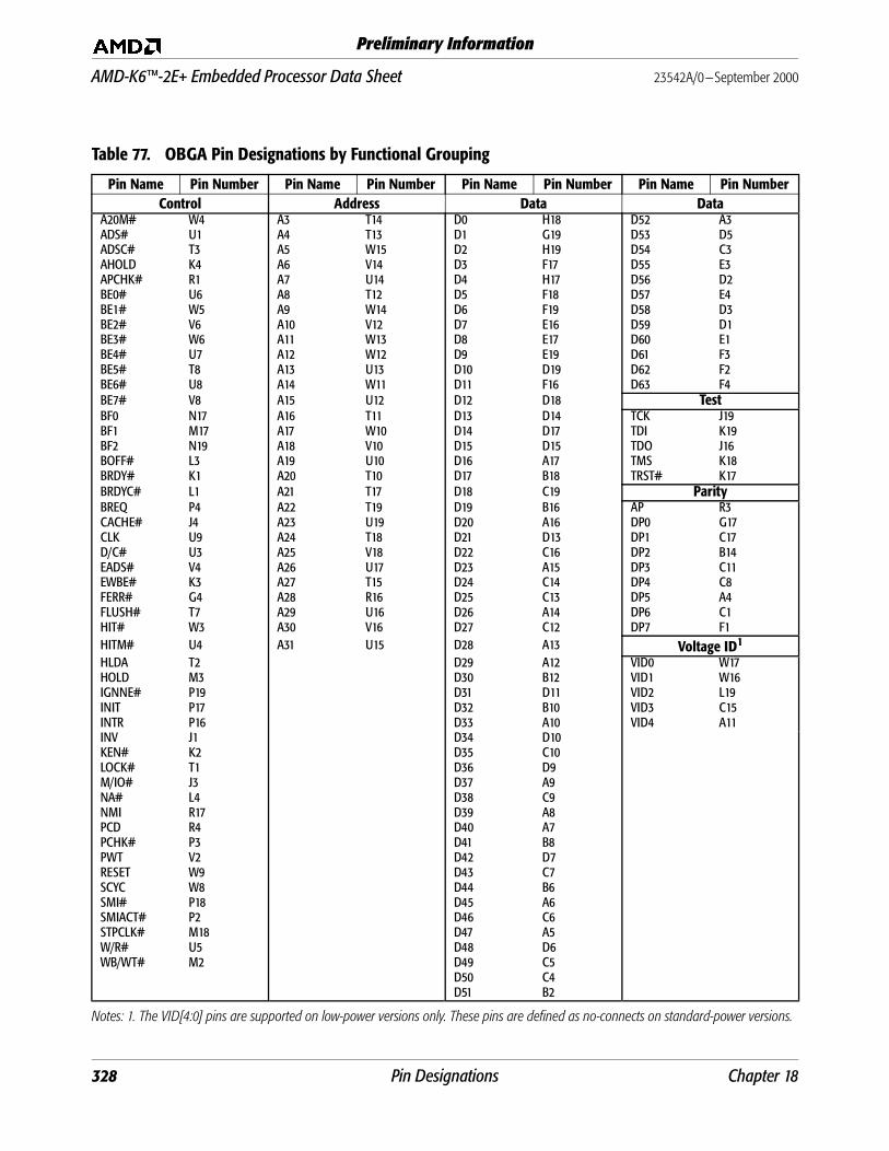
AMD-K6™-2E+ Embedded Processor Data Sheet 23542A/0—September 2000
Preliminary Information
Notes: 1. The VID[4:0] pins are supported on low-power versions only. These pins are defined as no-connects on standard-power versions.
Table 77. OBGA Pin Designations by Functional Grouping
Pin Name Pin Number Pin Name Pin Number Pin Name Pin Number Pin Name Pin NumberControl Address Data Data
A20M# W4 A3 T14 D0 H18 D52 A3ADS# U1 A4 T13 D1 G19 D53 D5ADSC# T3 A5 W15 D2 H19 D54 C3AHOLD K4 A6 V14 D3 F17 D55 E3APCHK# R1 A7 U14 D4 H17 D56 D2BE0# U6 A8 T12 D5 F18 D57 E4BE1# W5 A9 W14 D6 F19 D58 D3BE2# V6 A10 V12 D7 E16 D59 D1BE3# W6 A11 W13 D8 E17 D60 E1BE4# U7 A12 W12 D9 E19 D61 F3BE5# T8 A13 U13 D10 D19 D62 F2BE6# U8 A14 W11 D11 F16 D63 F4BE7# V8 A15 U12 D12 D18 TestBF0 N17 A16 T11 D13 D14 TCK J19BF1 M17 A17 W10 D14 D17 TDI K19BF2 N19 A18 V10 D15 D15 TDO J16BOFF# L3 A19 U10 D16 A17 TMS K18BRDY# K1 A20 T10 D17 B18 TRST# K17BRDYC# L1 A21 T17 D18 C19 ParityBREQ P4 A22 T19 D19 B16 AP R3CACHE# J4 A23 U19 D20 A16 DP0 G17CLK U9 A24 T18 D21 D13 DP1 C17D/C# U3 A25 V18 D22 C16 DP2 B14EADS# V4 A26 U17 D23 A15 DP3 C11EWBE# K3 A27 T15 D24 C14 DP4 C8FERR# G4 A28 R16 D25 C13 DP5 A4FLUSH# T7 A29 U16 D26 A14 DP6 C1HIT# W3 A30 V16 D27 C12 DP7 F1HITM# U4 A31 U15 D28 A13 Voltage ID1
HLDA T2 D29 A12 VID0 W17HOLD M3 D30 B12 VID1 W16IGNNE# P19 D31 D11 VID2 L19INIT P17 D32 B10 VID3 C15INTR P16 D33 A10 VID4 A11INV J1 D34 D10KEN# K2 D35 C10LOCK# T1 D36 D9M/IO# J3 D37 A9NA# L4 D38 C9NMI R17 D39 A8PCD R4 D40 A7PCHK# P3 D41 B8PWT V2 D42 D7RESET W9 D43 C7SCYC W8 D44 B6SMI# P18 D45 A6SMIACT# P2 D46 C6STPCLK# M18 D47 A5W/R# U5 D48 D6WB/WT# M2 D49 C5
D50 C4D51 B2
328 Pin Designations Chapter 18
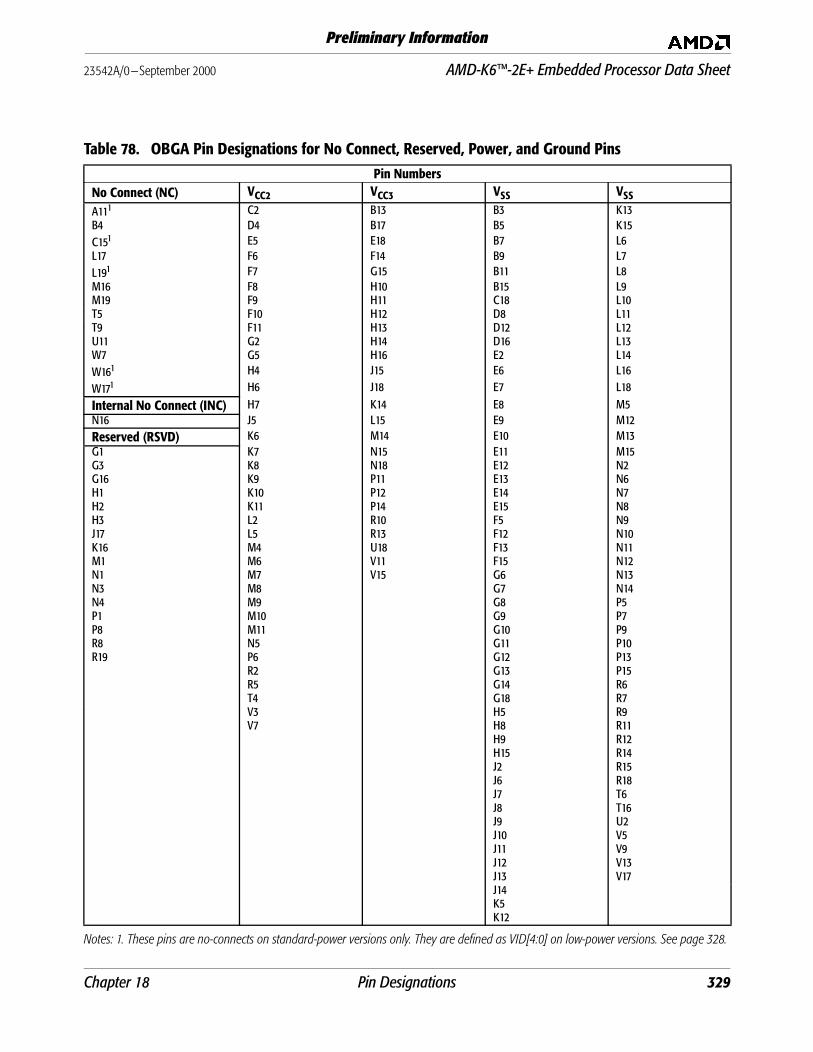
23542A/0—September 2000 AMD-K6™-2E+ Embedded Processor Data Sheet
Preliminary Information
Notes: 1. These pins are no-connects on standard-power versions only. They are defined as VID[4:0] on low-power versions. See page 328.
Table 78. OBGA Pin Designations for No Connect, Reserved, Power, and Ground PinsPin Numbers
No Connect (NC) VCC2 VCC3 VSS VSS A111 C2 B13 B3 K13B4 D4 B17 B5 K15C151 E5 E18 B7 L6L17 F6 F14 B9 L7L191 F7 G15 B11 L8M16 F8 H10 B15 L9M19 F9 H11 C18 L10T5 F10 H12 D8 L11T9 F11 H13 D12 L12U11 G2 H14 D16 L13W7 G5 H16 E2 L14W161 H4 J15 E6 L16
W171 H6 J18 E7 L18
Internal No Connect (INC) H7 K14 E8 M5N16 J5 L15 E9 M12Reserved (RSVD) K6 M14 E10 M13G1 K7 N15 E11 M15G3 K8 N18 E12 N2G16 K9 P11 E13 N6H1 K10 P12 E14 N7H2 K11 P14 E15 N8H3 L2 R10 F5 N9J17 L5 R13 F12 N10K16 M4 U18 F13 N11M1 M6 V11 F15 N12N1 M7 V15 G6 N13N3 M8 G7 N14N4 M9 G8 P5P1 M10 G9 P7P8 M11 G10 P9R8 N5 G11 P10R19 P6 G12 P13
R2 G13 P15R5 G14 R6T4 G18 R7V3 H5 R9V7 H8 R11
H9 R12H15 R14J2 R15J6 R18J7 T6J8 T16J9 U2J10 V5J11 V9J12 V13J13 V17J14K5K12
Chapter 18 Pin Designations 329

AMD-K6™-2E+ Embedded Processor Data Sheet 23542A/0—September 2000
Preliminary Information
330 Pin Designations Chapter 18

23542A/0—September 2000 AMD-K6™-2E+ Embedded Processor Data Sheet
Preliminary Information
19 Package Specifications
19.1 321-Pin Staggered CPGA Package Specification
Figure 125. 321-Pin Staggered CPGA Package Specification
Chapter 19 Package Specifications 331
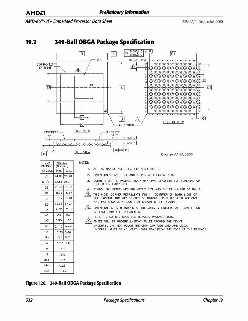
AMD-K6™-2E+ Embedded Processor Data Sheet 23542A/0—September 2000
Preliminary Information
19.2 349-Ball OBGA Package Specification
Figure 126. 349-Ball OBGA Package Specification
Dwg rev. AA.04; 08/00
332 Package Specifications Chapter 19
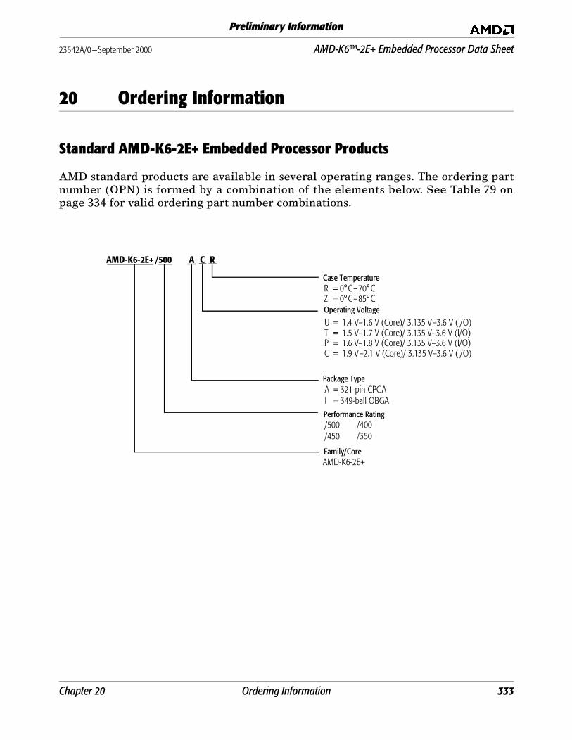
23542A/0—September 2000 AMD-K6™-2E+ Embedded Processor Data Sheet
Preliminary Information
20 Ordering Information
Standard AMD-K6-2E+ Embedded Processor Products
AMD standard products are available in several operating ranges. The ordering partnumber (OPN) is formed by a combination of the elements below. See Table 79 onpage 334 for valid ordering part number combinations.
AAMD-K6-2E+
Case TemperatureR = 0°C–70°CZ = 0°C–85°C
/500
Operating Voltage
U = 1.4 V–1.6 V (Core)/ 3.135 V–3.6 V (I/O)T = 1.5 V–1.7 V (Core)/ 3.135 V–3.6 V (I/O)P = 1.6 V–1.8 V (Core)/ 3.135 V–3.6 V (I/O)C = 1.9 V–2.1 V (Core)/ 3.135 V–3.6 V (I/O)
C R
Package Type
Family/Core
A = 321-pin CPGAI = 349-ball OBGA
AMD-K6-2E+
Performance Rating/500/450
/400/350
Chapter 20 Ordering Information 333

AMD-K6™-2E+ Embedded Processor Data Sheet 23542A/0—September 2000
Preliminary Information
Table 79. AMD-K6™-2E+ Embedded Processor Valid Ordering Part Number Combinations
Device Type OPN1
Notes:1. This table lists configurations planned to be supported in volume for this device. Consult the local AMD sales office to confirm
availability of specific valid combinations and to check on newly-released combinations.
Package Type Operating Voltage Case Temperature
Maximum CPU/Bus Frequency
Low Power
AMD-K6-2E+/350AUZ 321-pin CPGA1.4 V–1.6 V (Core)3.135 V–3.6 V (I/O)
0°C–85°C 350 MHz/100 MHz
AMD-K6-2E+/400ATZ 321-pin CPGA1.5 V–1.7 V (Core)
3.135 V–3.6 V (I/O)0°C–85°C 400 MHz/100 MHz
AMD-K6-2E+/450APZ 321-pin CPGA1.6 V–1.8 V (Core)3.135 V–3.6 V (I/O)
0°C–85°C 450 MHz/100 MHz
AMD-K6-2E+/350IUZ 349-ball OBGA1.4 V–1.6 V (Core)3.135 V–3.6 V (I/O)
0°C–85°C 350 MHz/100 MHz
AMD-K6-2E+/400ITZ 349-ball OBGA1.5 V–1.7 V (Core)
3.135 V–3.6 V (I/O)0°C–85°C 400 MHz/100 MHz
Standard Power
AMD-K6-2E+/400ACR 321-pin CPGA1.9 V–2.1 V (Core)3.135 V–3.6 V (I/O)
0°C–70°C 400 MHz/100 MHz
AMD-K6-2E+/450ACR 321-pin CPGA1.9 V–2.1 V (Core)
3.135 V–3.6 V (I/O)0°C–70°C 450 MHz/100 MHz
AMD-K6-2E+/500ACR 321-pin CPGA1.9 V–2.1V (Core)
3.135 V–3.6 V (I/O)0°C–70°C 500 MHz/100 MHz
AMD-K6-2E+/400ICR 349-ball OBGA1.9 V–2.1 V (Core)3.135 V–3.6 V (I/O)
0°C–70°C 400 MHz/100 MHz
AMD-K6-2E+/450ICR 349-ball OBGA1.9 V–2.1 V (Core)
3.135 V–3.6 V (I/O)0°C–70°C 450 MHz/100 MHz
334 Ordering Information Chapter 20
23542A/0—September 2000 AMD-K6™-2E+ Embedded Processor Data Sheet
Preliminary Information
Index
Numerics0.18-Micron Process Technology . . . . . . . . . . . . . . . . . . . . . . . 7100-MHz Bus
clock switching characteristics . . . . . . . . . . . . . . . . . . . . 296frontside. . . . . . . . . . . . . . . . . . . . . . . . . . . . . . . . . . . . . . . 1, 8input setup and hold timings. . . . . . . . . . . . . . . . . . . . . . 300output delay timings. . . . . . . . . . . . . . . . . . . . . . . . . . . . . 298Super7 platform support . . . . . . . . . . . . . . . . . . . . . . . . . 1, 8
321-Pin Staggered CPGA Package . . . . . . . . . . . . . . . . . . . . . 2specification . . . . . . . . . . . . . . . . . . . . . . . . . . . . . . . . . . . 331
349-Ball OBGA Packagespecification . . . . . . . . . . . . . . . . . . . . . . . . . . . . . . . . . . . 332
3DNow!™ Technology. . . . . . . 2, 5, 7, 15, 17, 19, 21–24, 127data types . . . . . . . . . . . . . . . . . . . . . . . . . . . . . . . . . . . . . . 37execution unit . . . . . . . . . . . . . . . . . . . . . . . . . . . . . . . . . . . 24INIT state. . . . . . . . . . . . . . . . . . . . . . . . . . . . . . . . . . . . . . 203instruction compatibility, floating-point and. . . . . . . . . 240instructions . . . . . . . . . . . . . . . . . . . . . . . . . . . . . .89–90, 240PREFETCH instruction . . . . . . . . . . . . . . . . . . . . . . . . . . 220register operation . . . . . . . . . . . . . . . . . . . . . . . . . . . . . . . . 14registers . . . . . . . . . . . . . . . . . . . . . . . . . . . . . . . . . . . . . . . . 35RESET state . . . . . . . . . . . . . . . . . . . . . . . . . . . . . . . . . . . 199software prefetching. . . . . . . . . . . . . . . . . . . . . . . . . . . . . 220
66-MHz Busclock switching characteristics . . . . . . . . . . . . . . . . . . . . 297input setup and hold timings. . . . . . . . . . . . . . . . . . . . . . 304output delay timings. . . . . . . . . . . . . . . . . . . . . . . . . . . . . 302
AA[31:3] . . . . . . . . . . . . . . . . . . . . . . . . . . . . . . . . . . . . . . . . . . . 95A20M# Signal . . . . . . . . . . . . . . . . . . . . . . . . . . . . . . . . . 94, 242
masking cache accesses with . . . . . . . . . . . . . . . . . . . . . . 227Absolute Ratings. . . . . . . . . . . . . . . . . . . . . . . . . . . . . . . . . . 287Accelerated Graphic Port (AGP) . . . . . . . . . . . . . . . . . . . . . . . 8Acknowledge, Interrupt . . . . . . . . . . . . . . . . . . . . . . . . . . . . 188Address
bus . . . . . . . . . . . . . . . . . . . . . . . . . . . . . . . . . . . . . . . 100, 109A[31:3] signals] . . . . . . . . . . . . . . . . . . . . . . . . . . . . . . . . 95address hold signal . . . . . . . . . . . . . . . . . . . . . . . . . . . . . 97address strobe signal . . . . . . . . . . . . . . . . . . . . . . . . . . . 96AHOLD restriction . . . . . . . . . . . . . . . . . . . 174, 178, 180coherencey . . . . . . . . . . . . . . . . . . . . . . . . . . . . . . . . . . 222parity . . . . . . . . . . . . . . . . . . . . . . . . . . . . . . . . . . . . . 98–99
generation sequence during bursts (table) . . . . . . . . . . 162hold signal . . . . . . . . . . . . . . . . . . . . . . . . . . . . . . . . . . . . . . 97parity check signal . . . . . . . . . . . . . . . . . . . . . . . . . . . . . . . 99parity signal. . . . . . . . . . . . . . . . . . . . . . . . . . . . . . . . . . . . . 98
ADS# Signal. . . . . . . . . . . . . . . . . . . . . . . . . . . . . . . . . . . . . . . 96ADSC# Signal . . . . . . . . . . . . . . . . . . . . . . . . . . . . . . . . . . . . . 96AGP . . . . . . . . . . . . . . . . . . . . . . . . . . . . . . . . . . . . . . . . . . . . . . 8AHOLD
-initiated inquire hit to modified line. . . . . . . . . . . . . . . 178-initiated inquire hit to shared or exclusive line . . . . . . 176-initiated inquire miss . . . . . . . . . . . . . . . . . . . . . . . . . . . 174restriction . . . . . . . . . . . . . . . . . . . . . . . . . . . . . . . . . . . . . 180
AHOLD Signal. . . . . . . . . . . . . . . . . . . . . . . . . . . . . . . . . 97, 278
Airflowconsideration in layout . . . . . . . . . . . . . . . . . . . . . . . . . . .317heatsink with fan (figure). . . . . . . . . . . . . . . . . . . . . . . . .319management. . . . . . . . . . . . . . . . . . . . . . . . . . . . . . . . . . . .319path in a dual-fan system (figure) . . . . . . . . . . . . . . . . . .319path in an ATX form-factor system (figure) . . . . . . . . . .320
Aligned Transfers . . . . . . . . . . . . . . . . . . . . . . . . . . . . . . . . .129Allocate, Write. . . . . . . . . . . . . . . . . . . . . . . . . . . . . . . . . . . .215AMD PowerNow!™ Technology . . . . . . . . . . . 6, 143, 151, 275
disabling . . . . . . . . . . . . . . . . . . . . . . . . . . . . . . . . . . . . . . .145dynamic core voltage control . . . . . . . . . . . . . . . . . . . . . .151enabling . . . . . . . . . . . . . . . . . . . . . . . . . . . . . . . . . . . . . . .145enhanced power management register (EPMR) . . . . . .144EPM 16-byte I/O block . . . . . . . . . . . . . . . . . . . . . . . . . . .146EPM stop grant state. . . . . . . . . . . . . . . . . . . . . . . . . . . . .150I/O base address definition. . . . . . . . . . . . . . . . . . . . . . . .145processor state observability register (PSOR) . . . . . . . .148SMM handler . . . . . . . . . . . . . . . . . . . . . . . . . . . . . . . . . . .145voltage identification signals . . . . . . . . . . . . . . . . . 137, 151
AP Signal . . . . . . . . . . . . . . . . . . . . . . . . . . . . . . . . . . . . . . . . .98APCHK# Signal . . . . . . . . . . . . . . . . . . . . . . . . . . . . . . . . . . . .99Asserted signal . . . . . . . . . . . . . . . . . . . . . . . . . . . . . . . . . . . .93
BBackoff . . . . . . . . . . . . . . . . . . . . . . . . . . . . . . . . . . . . . . . . . .102BDC Bit . . . . . . . . . . . . . . . . . . . . . . . . . . . . . . . . . . . . . . . . . .147BE[7:0]# Signal . . . . . . . . . . . . . . . . . . . . . . . . . . . . . . . . . . .100BF[2:0] . . . . . . . . . . . . . . . . . . . . . . . . . . . . . . . . . 101, 199, 283BIOS, enhanced power management. . . . . . . . . . . . . . . . . .145BIST . . . . . . . . . . . . . . . . . . . . . . . . . . . . . . . . . . . . . . . . . . . .251Block Diagram . . . . . . . . . . . . . . . . . . . . . . . . . . . . . . . . . . . . .12BOFF# Signal . . . . . . . . . . . . . . . . . . . . . . . . . . . . . . . . 102, 182
locked operation with . . . . . . . . . . . . . . . . . . . . . . . . . . . .186Boundary-Scan
bit definitions (table) . . . . . . . . . . . . . . . . . . . . . . . . . . . .257register (BSR) . . . . . . . . . . . . . . . . . . . . . . . . . . . . . . . . . .255test access port (TAP) . . . . . . . . . . . . . . . . . . . . . . . . . . . .253
BR . . . . . . . . . . . . . . . . . . . . . . . . . . . . . . . . . . . . . . . . . . . . . .259Branch
execution . . . . . . . . . . . . . . . . . . . . . . . . . . . . . . . . . . . . . . .26history table . . . . . . . . . . . . . . . . . . . . . . . . . . . . . . . . . . . . .25prediction . . . . . . . . . . . . . . . . . . . . . . . . . . . .1, 7, 15, 23, 26target cache . . . . . . . . . . . . . . . . . . . . . . . . . . . . . . . . . . . . .26
BRDY# Signal . . . . . . . . . . . . . . . . . . . . . . . . . . . . . . . . . . . .103BRDYC# Signal . . . . . . . . . . . . . . . . . . . . . . . . . . . . . . . . . . .104BREQ Signal . . . . . . . . . . . . . . . . . . . . . . . . . . . . . . . . . . . . .104BSR . . . . . . . . . . . . . . . . . . . . . . . . . . . . . . . . . . . . . . . . . . . . .255Built-In Self-Test (BIST) . . . . . . . . . . . . . . . . . . . . . . . . . . . .251Burst
pipelined burst reads . . . . . . . . . . . . . . . . . . . . . . . . . . . .162reads . . . . . . . . . . . . . . . . . . . . . . . . . . . . . . . . . . . . . . . . . .162ready . . . . . . . . . . . . . . . . . . . . . . . . . . . . . . . . . . . . . . . . . .103ready copy . . . . . . . . . . . . . . . . . . . . . . . . . . . . . . . . 104, 200writeback . . . . . . . . . . . . . . . . . . . . . . . . . . . . . . . . . . . . . .164writeback due to cache-line replacement . . . . . . . .164–165
Bus100-MHz . . . . . . . . . . . . . . . . . . . . . . . . . . . . . . . . . . . . . . 1, 8address . . . . . . . . . . . . . . . . . . . . . . . . . . . . . . . . . . . . . . . .178
A[31:0] . . . . . . . . . . . . . . . . . . . . . . . . . . . . . . . . . . . . . . .95AHOLD restriction . . . . . . . . . . . . . . . . . . . . . . . . . . . .180
Index 335
AMD-K6™-2E+ Embedded Processor Data Sheet 23542A/0—September 2000
Preliminary Information
coherency . . . . . . . . . . . . . . . . . . . . . . . . . . . . . . . . . . . 222external address strobe signal. . . . . . . . . . . . . . . . . . . 109hold signal . . . . . . . . . . . . . . . . . . . . . . . . . . . . . . . . . . . . 97inquire cycles . . . . . . . . . . . . . . . . . . . . . . . . . . . . 100, 174parity . . . . . . . . . . . . . . . . . . . . . . . . . . . . . . . . . . . . . 98–99strobe copy signal . . . . . . . . . . . . . . . . . . . . . . . . . . . . . . 96strobe signal . . . . . . . . . . . . . . . . . . . . . . . . . . . . . . . . . . 96valid . . . . . . . . . . . . . . . . . . . . . . . . . . . . . . . . . . . . . . . . 109
arbitration cycles, inquire and . . . . . . . . . . . . . . . . . . . . 168backoff . . . . . . . . . . . . . . . . . . . . . . . . . . . . . . . . . . . . . . . . 182byte enable signals . . . . . . . . . . . . . . . . . . . . . . . . . . . . . . 100cycles . . . . . . . . . . . . . . . . . . . . . . . . . . . . . . . . . . . . . 153–197
aligned transfers. . . . . . . . . . . . . . . . . . . . . . . . . . . . . . 129definitions (table) . . . . . . . . . . . . . . . . . . . . . . . . . . . . . 142order during misaligned I/O transfers (table) . . . . . . 167order during misaligned memory transfers (table). . 160special . . . . . . . . . . . . . . . . . . . . . . . . . . . . . . . . . .142, 190
data. . . . . . . . . . . . . . . . . . . . . . . . . . . . . . . . . . . 97, 103, 174AHOLD restriction . . . . . . . . . . . . . . . . . . . . . . . . . . . . 180aligned transfers. . . . . . . . . . . . . . . . . . . . . . . . . . . . . . 129byte enables . . . . . . . . . . . . . . . . . . . . . . . . . . . . . . . . . 100D[63:0] . . . . . . . . . . . . . . . . . . . . . . . . . . . . . . . . . . . . . . 107memory reads and writes. . . . . . . . . . . . . . . . . . . . . . . 158misaligned transfers . . . . . . . . . . . . . . . . . . . . . . .129, 184parity . . . . . . . . . . . . . . . . . . . . . . . . . . . . . . . . . . .108, 125state . . . . . . . . . . . . . . . . . . . . . . . . . . . . . . . . . . . . . . . . 156transition . . . . . . . . . . . . . . . . . . . . . . . . . . . . . . . . . . . . 157
frequency signals . . . . . . . . . . . . . . . . . . . . . . . . . . . . . . . 101hold request signal . . . . . . . . . . . . . . . . . . . . . . . . . . . . . . 115lock signal . . . . . . . . . . . . . . . . . . . . . . . . . . . . . . . . . . . . . 120request signal . . . . . . . . . . . . . . . . . . . . . . . . . . . . . . . . . . 104states
address . . . . . . . . . . . . . . . . . . . . . . . . . . . . . . . . . . . . . . 156data . . . . . . . . . . . . . . . . . . . . . . . . . . . . . . . . . . . . . . . . 156data-NA# requested . . . . . . . . . . . . . . . . . . . . . . . . . . . 156idle . . . . . . . . . . . . . . . . . . . . . . . . . . . . . . . . . . . . . . . . . 156pipeline address . . . . . . . . . . . . . . . . . . . . . . . . . . . . . . 156pipeline data . . . . . . . . . . . . . . . . . . . . . . . . . . . . . . . . . 157state machine (figure) . . . . . . . . . . . . . . . . . . . . . . . . . 155transition . . . . . . . . . . . . . . . . . . . . . . . . . . . . . . . . . . . . 157
BVC Field. . . . . . . . . . . . . . . . . . . . . . . . . . . . . . . . . . . . . . . . 146definition (table). . . . . . . . . . . . . . . . . . . . . . . . . . . . . . . . 147
BVCM Bit . . . . . . . . . . . . . . . . . . . . . . . . . . . . . . . . . . . . . . . . 147BYPASS Instruction . . . . . . . . . . . . . . . . . . . . . . . . . . . . . . . 260Bypass Register (BR) . . . . . . . . . . . . . . . . . . . . . . . . . . . . . . 259
CCache . . . . . . . . . . . . . . . . . . . . . . . . . . . . . . . . . . . . . . . . . . . 263
branch target . . . . . . . . . . . . . . . . . . . . . . . . . . . . . . . . . . . . 26burst writeback cycles . . . . . . . . . . . . . . . . . . . . . . . . . . . 164cacheable access . . . . . . . . . . . . . . . . . . . . . . . . . . . . . . . . 105coherency. . . . . . . . . . . . . . . . . . . . . . . . . . . . . . . . . . . . . . 222
writeback. . . . . . . . . . . . . . . . . . . . . . . . . . . . . . . . . . . . 227writethrough . . . . . . . . . . . . . . . . . . . . . . . . . . . . . . . . . 227
control . . . . . . . . . . . . . . . . . . . . . . . . . . . . . . . . . . . . . . . . 229data cache . . . . . . . . . . . . . . . . . . . . . . . . . . . . . . . . . . . . . . 16disabling . . . . . . . . . . . . . . . . . . . . . . . . . . 46, 211, 251, 263enabling . . . . . . . . . . . . . . . . . . . . . . . . . . . . . . . . . . . . . . . 119flushing . . . . . . . . . . . . . . . . . . . . . . . . . . . . . . . . . . .112, 191inhibiting . . . . . . . . . . . . . . . . . . . . . . . . . . . . . . . . . . 251, 263inquire cycles . . . . . . . . . . . . . . . . . . . . . . . . . 168, 174, 178inquire cycles (table) . . . . . . . . . . . . . . . . . . . . . . . . . . . . 225
instruction cache . . . . . . . . . . . . . . . . . . . . . . . . . . . . . . . . .16instruction fetch and decode . . . . . . . . . . . . . . . . . . . . . . .17instruction prefetch. . . . . . . . . . . . . . . . . . . . . . . 16–17, 220L1 cache
cache-line replacement. . . . . . . . . . . . . . . . . . . . . . . . .214coherency states . . . . . . . . . . . . . . . . . . . . . . . . . . . . . .227data cache . . . . . . . . . . . . . . . . . . . . . . . . . . . . . . . . . . . .16data cache line (figure). . . . . . . . . . . . . . . . . . . . . . . . .207instruction cache . . . . . . . . . . . . . . . . . . . . . . . . . . . . . . .16instruction cache line (figure) . . . . . . . . . . . . . . . . . . .207internal snooping. . . . . . . . . . . . . . . . . . . . . . . . . . . . . .223organization . . . . . . . . . . . . . . . . . . . . . . . . . . . . . . . . . .205write allocate . . . . . . . . . . . . . . . . . . . . . . . . . . . . . . . . .215
L2 cachecache line (figure) . . . . . . . . . . . . . . . . . . . . . . . . . . . . .207cache-line replacement. . . . . . . . . . . . . . . . . . . . . . . . .214data reads. . . . . . . . . . . . . . . . . . . . . . . . . . . . . . . . . . . .266direct access. . . . . . . . . . . . . . . . . . . . . . . . . . . . . . . . . . .50disabling for debug . . . . . . . . . . . . . . . . . . . . . . . . . . . . .47EDX register content . . . . . . . . . . . . . . . . . . . . . . . . . .265Level-2 Cache Array Access Register (L2AAR). . . . . .50organization . . . . . . . . . . . . . . . . . . . . . . . . . . . . . . . . . .205RDMSR instruction effect . . . . . . . . . . . . . . . . . . . . . .265sector and line organization (figure). . . . . . . . . . . . . .265tag array testing . . . . . . . . . . . . . . . . . . . . . . . . . 213, 264tag information (figure) . . . . . . . . . . . . . . . . . . . . . . . . .52tag or data location (figure) . . . . . . . . . . . . . . . . . . . . . .51testing . . . . . . . . . . . . . . . . . . . . . . . . . . . . . . . . . . . . . . .264WRMSR instruction effect . . . . . . . . . . . . . . . . . . . . . .265
L3 cachedebugging. . . . . . . . . . . . . . . . . . . . . . . . . . . . . . . . . . . .263PCD signal . . . . . . . . . . . . . . . . . . . . . . . . . . . . . . . . . . .264testing . . . . . . . . . . . . . . . . . . . . . . . . . . . . . . . . . . . . . . .263
Level-2 Cache Array Access Register (L2AAR) . . . . . . .264-line fills . . . . . . . . . . . . . . . . . . . . . . . . . . . . . . . . . . 213, 264-line replacement. . . . . . . . . . . . . . . . . . . . . . . . . . . 214, 224masking cache accesses with A20M# . . . . . . . . . . . . . . .227MESI states in the data. . . . . . . . . . . . . . . . . . . . . . . . . . .207operation . . . . . . . . . . . . . . . . . . . . . . . . . . . . . . . . . . . . . .208organization . . . . . . . . . . . . . . . . . . . . . . . . . . . . . . . . . . . .205organization (figure) . . . . . . . . . . . . . . . . . . . . . . . . . . . . .206predecode bits . . . . . . . . . . . . . . . . . . . . . . . . . . . 16–17, 208prefetching . . . . . . . . . . . . . . . . . . . . . . . . . . . . . . 16–17, 220sector organization . . . . . . . . . . . . . . . . . . . . . . . . . . . . . . .16sector organization (figure) . . . . . . . . . . . . . . . . . . . . . . . .16signals . . . . . . . . . . . . . . . . . . . . . . . . . . . . . . . . . . . . . . . . .211snooping . . . . . . . . . . . . . . . . . . . . . . . . . . . . . . . . . . . . . . .223states. . . . . . . . . . . . . . . . . . . . . . . . . . . . . . . . . . . . . . . . . .221states (table) . . . . . . . . . . . . . . . . . . . . . . . . . . . . . . . . . . .225Super7 platform support . . . . . . . . . . . . . . . . . . . . . . . . . . .8total internal . . . . . . . . . . . . . . . . . . . . . . . . . . . . . . . . . . . . .1TR12 . . . . . . . . . . . . . . . . . . . . . . . . . . . . . . . . . . . . . . . . . . .46translation lookaside buffers (TLBs). . . . . . . . . . . . . . . .205write allocate . . . . . . . . . . . . . . . . . . . . . . . . . . . . . . . . . . .215write cycle order . . . . . . . . . . . . . . . . . . . . . . . . . . . . . . . .229write merge buffer . . . . . . . . . . . . . . . . . . . . . . . . . . . . . .229write to a cacheable page . . . . . . . . . . . . . . . . . . . . . . . . .216writeback . . . . . . . . . . . . . . . . . . . . . . . . . . . . . . . . . . . 12, 16writethrough . . . . . . . . . . . . . . . . . . . . . . . . . . . . . . . . . . .227
CACHE# Signal . . . . . . . . . . . . . . . . . . . . . . . . . . . . . . . . . . .105generation (table) . . . . . . . . . . . . . . . . . . . . . . . . . . . . . . .210
Capacitance . . . . . . . . . . . . . . . . . . . . . . . . . . . . . . . . . . . . . .288capacitor placement . . . . . . . . . . . . . . . . . . . . . . . . . . . . .292large capacitive loads . . . . . . . . . . . . . . . . . . . . . . . . . . . .293
336 Index
23542A/0—September 2000 AMD-K6™-2E+ Embedded Processor Data Sheet
Preliminary Information
Capture-DR state . . . . . . . . . . . . . . . . . . . . . . . . . . . . . . . . . 262Capture-IR state . . . . . . . . . . . . . . . . . . . . . . . . . . . . . . . . . . 262Case Temperature. . . . . . . . . . . . . . . . . . . . . . . . . . . . . . . . . 317
extended . . . . . . . . . . . . . . . . . . . . . . . . . . . . . . . . . . . . . . 313measuring . . . . . . . . . . . . . . . . . . . . . . . . . . . . . . . . . . . . . 317
Centralized Scheduler . . . . . . . . . . . . . . . . . . . . . . . . . . . . . . 21CLK
switching characteristics100-MHz bus operation . . . . . . . . . . . . . . . . . . . . . . . . 29660-MHz bus operation . . . . . . . . . . . . . . . . . . . . . . . . . 297
CLK Signal. . . . . . . . . . . . . . . . . . . . . . . . . . . . . . . . . . . . . . . 105capacitance . . . . . . . . . . . . . . . . . . . . . . . . . . . . . . . . . . . . 288
Clock Control. . . . . . . . . . . . . . . . . . . . . . . . . . . . . . . . . 105, 275states . . . . . . . . . . . . . . . . . . . . . . . . . . . . . . . . . . . . . . . . . 275
enhanced power management stop grant . . . . . . . . . 275halt . . . . . . . . . . . . . . . . . . . . . . . . . . . . . . . . . . . . . . . . . 278normal . . . . . . . . . . . . . . . . . . . . . . . . . . . . . . . . . . . . . . 275state transitions (figure) . . . . . . . . . . . . . . . . . . . 276–277stop clock. . . . . . . . . . . . . . . . . . . . . . . . . . . . . . . . 193, 283stop grant. . . . . . . . . . . . . . . . . . . . . . . . . . . 193, 278, 281stop grant inquire . . . . . . . . . . . . . . . . . . . . . . . . . . . . . 280
switching characteristics100-MHz bus operation . . . . . . . . . . . . . . . . . . . . . . . . 29666-MHz bus operation . . . . . . . . . . . . . . . . . . . . . . . . . 297
Coherencycache . . . . . . . . . . . . . . . . . . . . . . . . . . . . . . . . . . . . . . . . . 222writeback . . . . . . . . . . . . . . . . . . . . . . . . . . . . . . . . . . . . . . 227writethrough . . . . . . . . . . . . . . . . . . . . . . . . . . . . . . . . . . . 227
Compatibility, Floating-Point, MMX, and 3DNow! Instructions . . . . . . . . . . . . . . . . . . . . . . . . . . . . . . . . 240
Component Placement . . . . . . . . . . . . . . . . . . . . . . . . . . . . . 292Configuration
power-on initialization . . . . . . . . . . . . . . . . . . . . . . . . . . . 199signal timing (figure) . . . . . . . . . . . . . . . . . . . . . . . . . . . . 311signal timing for 100-MHz bus operation (table) . . . . . . 306signal timing for 66-MHz bus operation . . . . . . . . . . . . . 307VCC pins . . . . . . . . . . . . . . . . . . . . . . . . . . . . . . . . . . . . . . 200
Connectionspin requirements. . . . . . . . . . . . . . . . . . . . . . . . . . . . . . . . 293power requirements . . . . . . . . . . . . . . . . . . . . . . . . . . . . . 291
Control Register 0 (CR0) . . . . . . . . . . . . . . . . . . . . . . . . . . . . 40Control Register 1 (CR1) . . . . . . . . . . . . . . . . . . . . . . . . . . . . 40Control Register 2 (CR2) . . . . . . . . . . . . . . . . . . . . . . . . . . . . 39Control Register 3 (CR3) . . . . . . . . . . . . . . . . . . . . . . . . . . . . 39Control Register 4 (CR4) . . . . . . . . . . . . . . . . . . . . . . . . . . . . 39Counter, Time Stamp . . . . . . . . . . . . . . . . . . . . . . . . . . . . . . . 46CPGA Package . . . . . . . . . . . . . . . . . . . . . . . . . . . . . . . . . . . 2–3
pin designations (figure) . . . . . . . . . . . . . . . . . . . . . . . . . 322pin designations by function (table) . . . . . . . . . . . . . . . . 324pin differences (table . . . . . . . . . . . . . . . . . . . . . . . . . . . . 321specification . . . . . . . . . . . . . . . . . . . . . . . . . . . . . . . . . . . 331
CR4 Register . . . . . . . . . . . . . . . . . . . . . . . . . . . . . . . . . . . . . . 46Customer Service . . . . . . . . . . . . . . . . . . . . . . . . . . . . . . . . . . iiiCycles
bus . . . . . . . . . . . . . . . . . . . . . . . . . . . . . . . . . . . . . . . . . . . 153hold and hold acknowledge . . . . . . . . . . . . . . . . . . . . . . . 168inquire . . . 94–99, 109, 113–114, 131, 139, 164, 168, 170, . . . . 172, 174, 176–178, 182, 186, 222, 263, 275, 278–280inquire and bus arbitration . . . . . . . . . . . . . . . . . . . . . . . 168interrupt acknowledge . . . . . . . . 95, 98, 100, 106, 123, 138locked . . . . . . . . . . . . . . . . . . . . . . . . . . . . . . . . . . . . . . . . . 184pipelined . . . . . . . . . . . . . . . . . . . . . . . . . . . . . . . . . . . .17, 96pipelined write . . . . . . . . . . . . . . . . . . . . . . . . . . . . . . . . . 107shutdown . . . . . . . . . . . . . . . . . . . . . . . . . . . . . . . . . . . . . . 192special bus . . . . . . . . . . . . . . . . . . . . . . . . . . . . . . . . . . . . . 190
writeback . . . . . . 94, 96–97, 110, 113, 139, 164, 172, 176, . . . . . . . . . . . . . . . . . . . . . 178, 180, 186, 210, 264, 277, 280
DD/C# Signal. . . . . . . . . . . . . . . . . . . . . . . . . . . . . . . . . . . . . . .106D[63:0] Signals. . . . . . . . . . . . . . . . . . . . . . . . . . . . . . . . . . . .107Data
busAHOLD restriction . . . . . . . . . . . . . . . . . . . . . . . . 97, 180AHOLD timing. . . . . . . . . . . . . . . . . . . . . . . . . . . . . . . .174aligned transfers . . . . . . . . . . . . . . . . . . . . . . . . . . . . . .129BRDY# timing . . . . . . . . . . . . . . . . . . . . . . . . . . . . . . . .103byte enable signals . . . . . . . . . . . . . . . . . . . . . . . . . . . .100D[63:0] signals . . . . . . . . . . . . . . . . . . . . . . . . . . . . . . . .107data state . . . . . . . . . . . . . . . . . . . . . . . . . . . . . . . . . . . .156memory reads and writes . . . . . . . . . . . . . . . . . . . . . . .158misaligned transfers . . . . . . . . . . . . . . . . . . . . . . 129, 184parity . . . . . . . . . . . . . . . . . . . . . . . . . . . . . . . . . . 108, 125split cycles . . . . . . . . . . . . . . . . . . . . . . . . . . . . . . . . . . .129transition . . . . . . . . . . . . . . . . . . . . . . . . . . . . . . . . . . . .157
cache . . . . . . . . . . . . . . . . . . . . . . . . . . . . . . . . . . . . . . . . . . .16MESI states . . . . . . . . . . . . . . . . . . . . . . . . . . . . . . . . . .207
parity . . . . . . . . . . . . . . . . . . . . . . . . . . . . . . . . . . . . . . . . .108types
3DNow!™ Technology. . . . . . . . . . . . . . . . . . . . . . . . . . .37floating-point register . . . . . . . . . . . . . . . . . . . . . . . . . . .34integer . . . . . . . . . . . . . . . . . . . . . . . . . . . . . . . . . . . . . . .29MMX technology . . . . . . . . . . . . . . . . . . . . . . . . . . . . . . .36
Data/Code Signal . . . . . . . . . . . . . . . . . . . . . . . . . . . . . . . . . .106Data-NA# Requested State. . . . . . . . . . . . . . . . . . . . . . . . . .156DC Characteristics. . . . . . . . . . . . . . . . . . . . . . . . . . . . . . . . .287Debug . . . . . . . . . . . . . . . . . . . . . . . . . . . . . . . . . . . . . . . . . . .268
exceptions . . . . . . . . . . . . . . . . . . . . . . . . . . . . . . . . . . . . .273registers . . . . . . . . . . . . . . . . . . . . . . . . . . . . . . . . . . . 41, 269
DR3–DR0 . . . . . . . . . . . . . . . . . . . . . . . . . . . . . . . . . . . .271DR5–DR4 . . . . . . . . . . . . . . . . . . . . . . . . . . . . . . . . . . . .271DR6 . . . . . . . . . . . . . . . . . . . . . . . . . . . . . . . . . . . . . . . . .272DR7 . . . . . . . . . . . . . . . . . . . . . . . . . . . . . . . . . . . . . . . . .272
System Management Mode (SMM) . . . . . . . . . . . . .249–250Decoders . . . . . . . . . . . . . . . . . . . . . . . . . . . . . . . . . . . . . . . . . .13Decoupling Recommendations . . . . . . . . . . . . . . . . . . . . . .292Descriptors and Gates . . . . . . . . . . . . . . . . . . . . . . . . . . . . . . .59Device Identification Register (DIR) . . . . . . . . . . . . . . . . .258Diagrams
key. . . . . . . . . . . . . . . . . . . . . . . . . . . . . . . . . . . . . . . . . . . .309timing . . . . . . . . . . . . . . . . . . . . . . . . . . . . . . . . 153, 309–312waveform definitions. . . . . . . . . . . . . . . . . . . . . . . . . . . . .153
Digital Signal Processing Instructions . . . . . . . . . . . . . . . . .90DIR . . . . . . . . . . . . . . . . . . . . . . . . . . . . . . . . . . . . . . . . . . . . .258Dissipation, Power . . . . . . . . . . . . . . . . . . . . . . . . . . . . . . . . .289Documentation . . . . . . . . . . . . . . . . . . . . . . . . . . . . . . . . . . . . iiiDP[7:0] Signals . . . . . . . . . . . . . . . . . . . . . . . . . . . . . . . . . . .108DR3–DR0 . . . . . . . . . . . . . . . . . . . . . . . . . . . . . . . . . . . . . . . .271DR5–DR4 . . . . . . . . . . . . . . . . . . . . . . . . . . . . . . . . . . . . . . . .271DR6 . . . . . . . . . . . . . . . . . . . . . . . . . . . . . . . . . . . . . . . . . . . . .272DR7 . . . . . . . . . . . . . . . . . . . . . . . . . . . . . . . . . . . . . . . . . . . . .272Driven signal . . . . . . . . . . . . . . . . . . . . . . . . . . . . . . . . . . . . . .93DSP Instructions . . . . . . . . . . . . . . . . . . . . . . . . . . . . . . 90, 239Dual Voltage. . . . . . . . . . . . . . . . . . . . . . . . . . . . . . . . . . . . . .291
Index 337
AMD-K6™-2E+ Embedded Processor Data Sheet 23542A/0—September 2000
Preliminary Information
EEADS# Signal . . . . . . . . . . . . . . . . . . . . . . . . . . . . . . . . . . . . 109EAS Register
time stamp counter value . . . . . . . . . . . . . . . . . . . . . . . . . 46EAX Register . . . . . . . . . . . . . . . . . . . . . . . . . . . . . . . . . . . . . 28
BIST results . . . . . . . . . . . . . . . . . . . . . . . . . . . . . . . . . . . . 202cache accesses . . . . . . . . . . . . . . . . . . . . . . . . . . . . . . . . . . . 51
EBF Field . . . . . . . . . . . . . . . . . . . . . . . . . . . . . . . . . . . . . . . . 150EBP Register . . . . . . . . . . . . . . . . . . . . . . . . . . . . . . . . . . . . . . 28EBX Register. . . . . . . . . . . . . . . . . . . . . . . . . . . . . . . . . . . . . . 28ECX Register. . . . . . . . . . . . . . . . . . . . . . . . . . . . . . . . . . . 28, 46EDI Register . . . . . . . . . . . . . . . . . . . . . . . . . . . . . . . . . . . . . . 28EDX Register . . . . . . . . . . . . . . . . . . . . . . . . . . . . . . . . . . . . . 28
cache accesses . . . . . . . . . . . . . . . . . . . . . . . . . . . . . . . . 50–51stepping ID . . . . . . . . . . . . . . . . . . . . . . . . . . . . . . . . . . . . 202time stamp counter value . . . . . . . . . . . . . . . . . . . . . . . . . 46
EFER . . . . . . . . . . . . . . . . . . . . . . . . . . . . . . . . 44, 47, 202, 229Effective Bus Frequency Divisor Field . . . . . . . . . . . . . . . . 150EFLAGS Register . . . . . . . . . . . . . . . . . . . . . . . . . . . . . . 38, 242EIP Register . . . . . . . . . . . . . . . . . . . . . . . . . . . . . . . . . . . . . 241Electrical Data . . . . . . . . . . . . . . . . . . . . . . . . . . . . . . . . . . . 285
absolute ratings. . . . . . . . . . . . . . . . . . . . . . . . . . . . . . . . . 287capacitance . . . . . . . . . . . . . . . . . . . . . . . . . . . . . . . . . . . . 288DC characteristics. . . . . . . . . . . . . . . . . . . . . . . . . . . . . . . 287operating ranges . . . . . . . . . . . . . . . . . . . . . . . . . . . . . . . . 285power and grounding . . . . . . . . . . . . . . . . . . . . . . . . . . . . 291power dissipation . . . . . . . . . . . . . . . . . . . . . . . . . . . . . . . 289
Embedded Processor Features . . . . . . . . . . . . . . . . . . . . . . . . 1EMMS Instruction. . . . . . . . . . . . . . . . . . . . . . . . . . . . . . . . . . 21EN Bit. . . . . . . . . . . . . . . . . . . . . . . . . . . . . . . . . . . . . . . . . . . 145Enhanced Power Management
special bus cycle (table) . . . . . . . . . . . . . . . . . . . . . . . . . . 142special bus cycles . . . . . . . . . . . . . . . . . . . . . . . . . . . . . . . 145stop grant state . . . . . . . . . . . . . . . . . . . . . . . . . . . . . . . . . 281
Enhanced Power Management Register (EPMR) . . . . . . . 144EPM 16-Byte I/O Block . . . . . . . . . . . . . . . . . . . . . . . . . . . . . 146EPM Stop Grant State . . . . . . . . . . . . . . . . . . . . . . . . . 142, 150
control . . . . . . . . . . . . . . . . . . . . . . . . . . . . . . . . . . . . . . . . 147voltage identification output state . . . . . . . . . . . . . . . . . 147
EPMR . . . . . . . . . . . . . . . . . . . . . . . . . . . . . . . . . . . . . . . . 44, 144ESI Register . . . . . . . . . . . . . . . . . . . . . . . . . . . . . . . . . . . . . . 28ESP Register . . . . . . . . . . . . . . . . . . . . . . . . . . . . . . . . . . . . . . 28EWBE# Control (EWBEC) . . . . . . . . . . . . . . . . . . . . . . . . . . 229EWBE# Signal . . . . . . . . . . . . . . . . . . . . . . . . . . . 110, 229, 278Exception. . . . 98–99, 108, 125, 192, 240, 249–250, 272–274
debug . . . . . . . . . . . . . . . . . . . . . . . . . . . . . . . . . . . . . . . . . 273flags . . . . . . . . . . . . . . . . . . . . . . . . . . . . . . . . . . . . . . . . 32–33floating-point. . . . . . . . . . . . . . . . . . 111, 116, 237–238, 240handler. . . . . . . . . . . . . . . . . . . . . . . . . . . . . . . . . . . . . . . . 268handling floating-point. . . . . . . . . . . . . . . . . . . . . . . . . . . 237machine check. . . . . . . . . . . . . . . . . . . . . . . . . . . . . . . . . . . 45MMX technology . . . . . . . . . . . . . . . . . . . . . . . . . . . . . . . . 240summary (table) . . . . . . . . . . . . . . . . . . . . . . . . . . . . . . . . . 62System Management Mode (SMM). . . . . . . . . . . . . . . . . 250
Executionlatency (table) . . . . . . . . . . . . . . . . . . . . . . . . . . . . . . . . . . . 23
Execution Units . . . . . . . . . . . . . . . . . . . . . . . . . . . . . . . . . . . . 13DNow!™ technology . . . . . . . . . . . . . . . . . . . . . . . . . . . . . 24branch . . . . . . . . . . . . . . . . . . . . . . . . . . . . . . . . . . . . . . 21, 26execution latency (table) . . . . . . . . . . . . . . . . . . . . . . . . . . 23floating-point. . . . . . . . . . . . . . . . . . . . . . . . . . . . . 3, 21, 237multimedia . . . . . . . . . . . . . . . . . . . . . . . . . . 21, 23–24, 239register X . . . . . . . . . . . . . . . . . . . . . . . . . . . . . . . . . . . . 21, 24
register Y . . . . . . . . . . . . . . . . . . . . . . . . . . . . . . . . . . . 21, 24throughput (table) . . . . . . . . . . . . . . . . . . . . . . . . . . . . . . . .23
Extended Feature Enable Register (EFER) . 44, 47, 202, 229External
address strobe signal. . . . . . . . . . . . . . . . . . . . . . . . . . . . .109write buffer empty signal . . . . . . . . . . . . . . . . . . . . . . . . .110
EXTEST Instruction . . . . . . . . . . . . . . . . . . . . . . . . . . . . . . .260
FFEMMS Instruction. . . . . . . . . . . . . . . . . . . . . . . . . . . . . . . . .21FERR# Signal . . . . . . . . . . . . . . . . . . . . . . . . . . . 111, 238, 240Float Conditions . . . . . . . . . . . . . . . . . . . . . . . . . . . . . 136, 141Floated signal . . . . . . . . . . . . . . . . . . . . . . . . . . . . . . . . . . . . .93Floating-Point
and MMX/3DNow! instruction compatibility . . . . . . . . .240and multimedia execution units . . . . . . . . . . . . . . . . . . .237error . . . . . . . . . . . . . . . . . . . . . . . . . . . . . . . . . . . . . . . . . .111execution unit . . . . . . . . . . . . . . . . . . . . . . . . . . . . . . . . . .237handling exceptions . . . . . . . . . . . . . . . . . . . . . . . . . . . . .237instructions (table) . . . . . . . . . . . . . . . . . . . . . . . . . . . . . . .82register data types. . . . . . . . . . . . . . . . . . . . . . . . . . . . . . . .34registers . . . . . . . . . . . . . . . . . . . . . . . . . . . . . . . . . . . . . . . .31
FLUSH# Signal . . . . . . . . . . . . . . . . . .112, 199, 223, 252, 278FPU
control word register . . . . . . . . . . . . . . . . . . . . . . . . . . . . . .33status word register. . . . . . . . . . . . . . . . . . . . . . . . . . . . . . .32tag word register . . . . . . . . . . . . . . . . . . . . . . . . . . . . . . . . .33
Frequency. . . . . . . . . . . . . . . . . . . . . . . . . . . 283, 296–297, 308control. . . . . . . . . . . . . . . . . . . . . . . . . . . . . . . . . . . . . . . . .151multiplier . . . . . . . . . . . . . . . . . . . . . . . . . . . . . . . . . . . . . .105operating . . . . . . . . . . . . . . . . . . . . . . . . . . . . . 101, 105, 199
GGate Descriptor . . . . . . . . . . . . . . . . . . . . . . . . . . . . . . . . 59, 62General-Purpose Registers . . . . . . . . . . . . . . . . . . . . . . . . . . .28Generate Special Bus Cycle Bit . . . . . . . . . . . . . . . . . . . . . .145Global EWBE# Disable (GEWBED). . . . . . . . . . . . . . . . . . .230Ground
pin designations (table) . . . . . . . . . . . . . . . . . . . . . 325, 329plane capacitance . . . . . . . . . . . . . . . . . . . . . . . . . . . . . . .292pulldown resistor . . . . . . . . . . . . . . . . . . . . . . . . . . . . . . . .293split planes . . . . . . . . . . . . . . . . . . . . . . . . . . . . . . . . . . . . .291unused active high inputs. . . . . . . . . . . . . . . . . . . . . . . . .293
GSBC Bit. . . . . . . . . . . . . . . . . . . . . . . . . . . . . . . . . . . . . . . . .145
HHalt
restart slot . . . . . . . . . . . . . . . . . . . . . . . . . . . . . . . . . . . . .246state . . . . . . . . . . . . . . . . . . . . . . . . . . . . . . . . . . . . . . . . . .278
Heat Dissipation Path . . . . . . . . . . . . . . . . . . . . . . . . . . . . . .316HIGHZ Instruction . . . . . . . . . . . . . . . . . . . . . . . . . . . . . . . .260Hit to
modified line . . . . . . . . . . . . . . . . . . . . . . . . . . . . . . . . . . .113modified line, AHOLD-initiated inquire. . . . . . . . . . . . .178modified line, HOLD-initiated inquire . . . . . . . . . . . . . .172shared or exclusive line, AHOLD-initiated inquire . . . .176shared or exclusive line, HOLD-initiated inquire . . . . .170
HIT# Signal . . . . . . . . . . . . . . . . . . . . . . . . . . . . . . . . . . . . . .113HITM# Signal. . . . . . . . . . . . . . . . . . . . . . . . . . . . . . . . . . . . .113HLDA Signal . . . . . . . . . . . . . . . . . . . . . . . . . . . . . . . . . . . . .114
338 Index

23542A/0—September 2000 AMD-K6™-2E+ Embedded Processor Data Sheet
Preliminary Information
Holdacknowledge cycle . . . . . . . . . . . . . . . . . . . . . . . . . . . . . . 168acknowledge signal. . . . . . . . . . . . . . . . . . . . . .114, 168–170
HOLD Signal . . . . . . . . . . . . . . . . . . . . . . . . . . . . . . . . . . . . . 115-initiated inquire hit to modified line. . . . . . . . . . . . . . . 172-initiated inquire hit to shared or exclusive line . . . . . . 170timing . . . . . . . . . . . . . . . . . . . . . . . . . . . . . . . . . . . . . 295, 310
II/O
misaligned read and write . . . . . . . . . . . . . . . . . . . . . . . . 167read and write . . . . . . . . . . . . . . . . . . . . . . . . . . . . . . . . . . 166trap doubleword . . . . . . . . . . . . . . . . . . . . . . . . . . . . . . . . 247trap restart slot . . . . . . . . . . . . . . . . . . . . . . . . . . . . . . . . . 248
IBF Field . . . . . . . . . . . . . . . . . . . . . . . . . . . . . . . . . . . . . . . . 147IDCODE Instruction . . . . . . . . . . . . . . . . . . . . . . . . . . . . . . . 260IEEE 1149.1 . . . . . . . . . . . . . . . . . . . . . . . . . . . . . . . . . . . . 2, 253IEEE 754 . . . . . . . . . . . . . . . . . . . . . . . . . . . . . . . . . . 2, 31, 237IEEE 854 . . . . . . . . . . . . . . . . . . . . . . . . . . . . . . . . . . . . . . . . 237IGNNE# Signal . . . . . . . . . . . . . . . . . . . . . . . . . . 116, 238, 240Ignore Numeric Exception . . . . . . . . . . . . . . . . . . . . . . . . . . 116INIT Signal . . . . . . . . . . . . . . . . . . . . . . . . . . . . . 117, 242, 278
-initiated transition from protected mode to real mode 196processor state after . . . . . . . . . . . . . . . . . . . . . . . . . . . . . 203
Initialization . . . . . . . . . . . . . . . . . . . . . . . . . . . . . . . . . . . . . 117output signal state . . . . . . . . . . . . . . . . . . . . . . . . . . . . . . 200power-on configuration. . . . . . . . . . . . . . . . . . . . . . . . . . . 199processor state after INIT . . . . . . . . . . . . . . . . . . . . . . . . 203processor state after RESET . . . . . . . . . . . . . . . . . . . . . . 200register state . . . . . . . . . . . . . . . . . . . . . . . . . . . . . . . . . . . 200RESET requirements . . . . . . . . . . . . . . . . . . . . . . . . . . . . 200signals sampled during RESET. . . . . . . . . . . . . . . . . . . . 199
Inputcapacitance . . . . . . . . . . . . . . . . . . . . . . . . . . . . . . . . . . . . 288leakage current . . . . . . . . . . . . . . . . . . . . . . . . . . . . . . . . . 288pin float conditions (table) . . . . . . . . . . . . . . . . . . . . . . . 141pin types (table) . . . . . . . . . . . . . . . . . . . . . . . . . . . . . . . . 140setup and hold timing
100-MHz bus operation . . . . . . . . . . . . . . . . . . . . . . . . 30066-MHz bus operation . . . . . . . . . . . . . . . . . . . . . . . . . 304
Input/Output (I/O)capacitance . . . . . . . . . . . . . . . . . . . . . . . . . . . . . . . . . . . . 288
Inquire . . . . . . . . . . . . . . . . . . . . . . . . . . . . . 171, 173, 175, 275bus arbitration cycles . . . . . . . . . . . . . . . . . . . . . . . . . . . . 168cycle hit . . . . . . . . . . . . . . . . . . . . . . . . . . . . . . . . . . . . . . . 113cycle hit to modified line . . . . . . . . . . . . . . . . . . . . . . . . . 113cycles . . . . . . . . .94–99, 109, 113–114, 131, 139, 164, 168, . . . . . . . . . . . 170, 172, 174, 176–178, 180, 182, 186, 222, . . . . . . . . . . . . . . . . . . . . . . . . . . . . . . . . . 263, 275, 278–280miss, AHOLD-initiated . . . . . . . . . . . . . . . . . . . . . . . . . . . 174
Instructions . . . . . . . . . . . . . . . . . . . . . . . . . . . . . . . . . . . . . . . 633DNow!™ technology . . . . . . . . . . . . . . . . . . . . . .89–90, 2393DNow!™ technology (table) . . . . . . . . . . . . . . . . . . . . 89–90cache . . . . . . . . . . . . . . . . . . . . . . . . . . . . . . . . . . . . . . . . . . 16decode . . . . . . . . . . . . . . . . . . . . . . . . . . . . . . . . . . . . . . . . . 18digital signal processing. . . . . . . . . . . . . . . . . . . . . . . . . . 239digital signal processing (table) . . . . . . . . . . . . . . . . . . . . 90EMMS. . . . . . . . . . . . . . . . . . . . . . . . . . . . . . . . . . . . . . . . . . 21FEMMS . . . . . . . . . . . . . . . . . . . . . . . . . . . . . . . . . . . . . . . . 21fetch . . . . . . . . . . . . . . . . . . . . . . . . . . . . . . . . . . . . . . . . . . . 17floating-point (table) . . . . . . . . . . . . . . . . . . . . . . . . . . . . . 82integer (table) . . . . . . . . . . . . . . . . . . . . . . . . . . . . . . . . . . . 65INVD . . . . . . . . . . . . . . . . . . . . . . . . . . . . . . . . . . . . . . . . . 224MMX technology . . . . . . . . . . . . . . . . . . . . . . . . . . . . . 86, 239
MMX technology (table) . . . . . . . . . . . . . . . . . . . . . . . . . . .86pointer . . . . . . . . . . . . . . . . . . . . . . . . . . . . . . . . . . . . . . . . .31PREFETCH . . . . . . . . . . . . . . . . . . . . . . . . . . . . . . . . 17, 220RSM . . . . . . . . . . . . . . . . . . . . . . . . . . . . . . . . . . . . . . . . . .241serializing . . . . . . . . . . . . . . . . . . . . . . . . . . . . . . . . . . . . . . .94supported by the processor (table) . . . . . . . . . . . . . . . . . .63Test Access Port (TAP) . . . . . . . . . . . . . . . . . . . . . . . . . . .259WBINVD . . . . . . . . . . . . . . . . . . . . . . . . . . . . . . . . . . . . . . .224
Integerdata registers . . . . . . . . . . . . . . . . . . . . . . . . . . . . . . . . . . . .29data types . . . . . . . . . . . . . . . . . . . . . . . . . . . . . . . . . . . . . . .29instructions (table) . . . . . . . . . . . . . . . . . . . . . . . . . . . . . . .65
Interrupts . . . . . . . . . 130, 188, 192, 196, 237–238, 240, 242, . . . . . . . . . . . . . . . . . . . . . . . . . . . . . . . . . . . . . . . . 250, 273, 280
01h. . . . . . . . . . . . . . . . . . . . . . . . . . . . . . . . . . . . . . . . . . . .27403h. . . . . . . . . . . . . . . . . . . . . . . . . . . . . . . . . . . . . . . . . . . .27410h. . . . . . . . . . . . . . . . . . . . . . . . . . . . . . . . . . . . . . . . . . . .237acknowledge. . . . . . . 95, 103, 106, 118, 120, 125, 184, 188acknowledge cycle definition (table) . . . . . . . . . . . . . . .188acknowledge cycles . . . . . . . . . . 95, 98, 100, 106, 123, 138clock grant state . . . . . . . . . . . . . . . . . . . . . . . . . . . . . . . .280descriptor table register . . . . . . . . . . . . . . . . . . . . . . . . . . .54flag . . . . . . . . . . . . . . . . . . . . . . . . . . . . . . . . . . . 38, 118, 130floating-point exceptions . . . . . . . . . . . . . . . . . . . . .237–238gate . . . . . . . . . . . . . . . . . . . . . . . . . . . . . . . . . . . . . . . . . . . .61INIT. . . . . . . . . . . . . . . . . . . . . . . . . . . . . . . . . . . . . . 196, 242INTR . . . . . . . . . . . . . . . . . . . . . . . . . . . . . . . . . . . . . . . . . .118IRQ13 . . . . . . . . . . . . . . . . . . . . . . . . . . . . . . . . . . . . . . . . .239MMX instructions . . . . . . . . . . . . . . . . . . . . . . . . . . . . . . .240NMI . . . . . . . . . . . . . . . . . . . . . . . . . . . . . . . . . . 123, 203, 242redirection bitmap. . . . . . . . . . . . . . . . . . . . . . . . . . . . . . . .55request . . . . . . . . . . . . . . . . . . . . . . . . . . . . . . . . . . . . . . . .118service routine . . . . . . . . . . . . . . . . . . . . . 118, 123, 238, 241STPCLK# . . . . . . . . . . . . . . . . . . . . . . . . . . . . . . . . . . . . . .193summary (table). . . . . . . . . . . . . . . . . . . . . . . . . . . . . . . . . .62system management . . . . . . . . . . . . . . . . . . . . . . . . . . . . .241type of. . . . . . . . . . . . . . . . . . . . . . . . . . . . . . . . . . . . . . . . . .62
INTR Signal . . . . . . . . . . . . . . . . . . . . . . . . . . . . . . . . . 118, 278INV Signal . . . . . . . . . . . . . . . . . . . . . . . . . . . . . . . . . . . . . . .118Invalidation Request. . . . . . . . . . . . . . . . . . . . . . . . . . . . . . .118INVD Instruction . . . . . . . . . . . . . . . . . . . . . . . . . . . . . . . . . .224IOBASE Field. . . . . . . . . . . . . . . . . . . . . . . . . . . . . . . . . . . . .145
KKEN# Signal. . . . . . . . . . . . . . . . . . . . . . . . . . . . . . . . . . . . . .119
LL1 Cache. . . . . . . . . . . . . . . . . . . . . . . . . . . . . . . . . . . . . . . . . .46
cache line (figure) . . . . . . . . . . . . . . . . . . . . . . . . . . . . . . .207cache-line replacements . . . . . . . . . . . . . . . . . . . . . . . . . .214coherency . . . . . . . . . . . . . . . . . . . . . . . . . . . . . . . . . 222, 227data cache line (figure). . . . . . . . . . . . . . . . . . . . . . . . . . .207disabling . . . . . . . . . . . . . . . . . . . . . . . . . . . . . . . 46, 211–212flushing. . . . . . . . . . . . . . . . . . . . . . . . . . . . . . . . . . . . . . . .223inquire cycles (table) . . . . . . . . . . . . . . . . . . . . . . . . . . . .225instruction cache line (figure) . . . . . . . . . . . . . . . . . . . . .207internal snooping. . . . . . . . . . . . . . . . . . . . . . . . . . . . . . . .223MESI states . . . . . . . . . . . . . . . . . . . . . . . . . . . . . . . . . . . .207organization . . . . . . . . . . . . . . . . . . . . . . . . . . . . . . . . . . . .205organization (figure) . . . . . . . . . . . . . . . . . . . . . . . . . . . . .206prefetching . . . . . . . . . . . . . . . . . . . . . . . . . . . . . . . . . . . . .220sector organization (figure) . . . . . . . . . . . . . . . . . . . . . . . .16
Index 339
AMD-K6™-2E+ Embedded Processor Data Sheet 23542A/0—September 2000
Preliminary Information
states (table) . . . . . . . . . . . . . . . . . . . . . . . . . . .221, 225–226write allocate. . . . . . . . . . . . . . . . . . . . . . . . . . . . . . . . . . . 215
L2 Cache . . . . . . . . . . . . . . . . . . . . . . . . . . . 112–113, 139, 142access type. . . . . . . . . . . . . . . . . . . . . . . . . . . . . . . . . . . . . 265built-in self test . . . . . . . . . . . . . . . . . . . . . . . . . . . . . . . . . 251cache line (figure). . . . . . . . . . . . . . . . . . . . . . . . . . . . . . . 207cache sector and line organization (figure) . . . . . . . . . . 265cache-line fills . . . . . . . . . . . . . . . . . . . . . . . . . . . . . . . . . . 214cache-line replacements. . . . . . . . . . . . . . . . . . . . . . . . . . 214coherency. . . . . . . . . . . . . . . . . . . . . . . . . . . . . . . . . . . . . . 222data location (figure) . . . . . . . . . . . . . . . . . . . . . . . . . . . . . 51data reads . . . . . . . . . . . . . . . . . . . . . . . . . . . . . . . . . . . . . 266direct access . . . . . . . . . . . . . . . . . . . . . . . . . . . . . . . . . . . . 50disabling . . . . . . . . . . . . . . . . . . . . . . . . . . . . . . . . . . 211–212disabling for debug. . . . . . . . . . . . . . . . . . . . . . . . . . . . . . . 47flushing . . . . . . . . . . . . . . . . . . . . . . . . . . . . . . . . . . . . . . . 223inquire cycles (table) . . . . . . . . . . . . . . . . . . . . . . . . . . . . 225least recently used (LRU) algorithm . . . . . . . . . . . . . . . 215Level-2 Cache Array Access Register (L2AAR). . . . . . . . 50LRU field . . . . . . . . . . . . . . . . . . . . . . . . . . . . . . . . . . . . . . 267MESI states . . . . . . . . . . . . . . . . . . . . . . . . . . . . . . . . . . . . 207operation . . . . . . . . . . . . . . . . . . . . . . . . . . . . . . . . . . . . . . 209organization. . . . . . . . . . . . . . . . . . . . . . . . . . . . . . . . . . . . 205organization (figure). . . . . . . . . . . . . . . . . . . . . . . . .206, 265predecode bits not stored. . . . . . . . . . . . . . . . . . . . . . . . . 208prefetching . . . . . . . . . . . . . . . . . . . . . . . . . . . . . . . . . . . . 220sector organization (figure) . . . . . . . . . . . . . . . . . . . . . . . . 16states (table) . . . . . . . . . . . . . . . . . . . . . . . . . . .221, 225–226Super7 platform support . . . . . . . . . . . . . . . . . . . . . . . . . . . 8T/D bit . . . . . . . . . . . . . . . . . . . . . . . . . . . . . . . . . . . . . . . . 265tag array testing . . . . . . . . . . . . . . . . . . . . . . . . . . . . 213, 264tag information (figure) . . . . . . . . . . . . . . . . . . . . . . . . . . . 52tag location (figure) . . . . . . . . . . . . . . . . . . . . . . . . . . . . . . 51testing . . . . . . . . . . . . . . . . . . . . . . . . . . . . . . . . . . . . . . . . 264write allocate. . . . . . . . . . . . . . . . . . . . . . . . . . . . . . . . . . . 215
L2AAR . . . . . . . . . . . . . . . . . . . . . . . 44, 50, 212–213, 264–266L3 Cache
debugging . . . . . . . . . . . . . . . . . . . . . . . . . . . . . . . . . . . . . 263PCD signal . . . . . . . . . . . . . . . . . . . . . . . . . . . . . . . . . . . . . 264testing . . . . . . . . . . . . . . . . . . . . . . . . . . . . . . . . . . . . . . . . 263
Latency, execution (table) . . . . . . . . . . . . . . . . . . . . . . . . . . . 23Layout and Airflow Considerations . . . . . . . . . . . . . . . . . . 317Level-2 Cache Array Access Register (L2AAR). . . . . 264–266Literature. . . . . . . . . . . . . . . . . . . . . . . . . . . . . . . . . . . . . . . . . iiiLOCK# Signal . . . . . . . . . . . . . . . . . . . . . . . . . . . . . . . . . . . . 120Locked
cycles . . . . . . . . . . . . . . . . . . . . . . . . . . . . . . . . . . . . . . . . . 184operation with BOFF# intervention . . . . . . . . . . . . . . . . 186operation, basic. . . . . . . . . . . . . . . . . . . . . . . . . . . . . . . . . 184
Logicbranch-prediction . . . . . . . . . . . . . . . . . . . . . . 15, 23, 25–26external support of floating-point exceptions . . . . . . . . 238symbol (figure) . . . . . . . . . . . . . . . . . . . . . . . . . . . . . . . . . . 91
Low-Power Devices . . . . . . . . . . . . . . . . . . . . . 4, 286, 289, 334
MM/IO# Signal . . . . . . . . . . . . . . . . . . . . . . . . . . . . . . . . . . . . . 121Machine Check Address Register (MCAR) . . . . . .44–45, 202Machine Check Exception . . . . . . . . . . . . . . . . . . . . . . . . . . . 45Machine Check Type Register (MCTR) . . . . . . . . .44–45, 202Maskable Interrupt. . . . . . . . . . . . . . . . . . . . . . . . . . . . . . . . 118MCAR. . . . . . . . . . . . . . . . . . . . . . . . . . . . . . . . . . . . .44–45, 202MCTR . . . . . . . . . . . . . . . . . . . . . . . . . . . . . . . . . . . . .44–45, 202
Memorymanagement registers. . . . . . . . . . . . . . . . . . . . . . . . . . . . .54or I/O . . . . . . . . . . . . . . . . . . . . . . . . . . . . . . . . . . . . . . . . . .121read and write, misaligned single-transfer . . . . . . . . . . .160read and write, single-transfer. . . . . . . . . . . . . . . . . . . . .158reads and writes . . . . . . . . . . . . . . . . . . . . . . . . . . . . . . . .158type range registers (MTRR) . . . . . . . . . . . . . . . . . . 49, 231
MESI . . . . . . . . . . . . . . . . . . . . . . . . . . . . .1, 168, 172, 206, 227bit . . . . . . . . . . . . . . . . . . . . . . . . . . . . . . . . . . . . 16, 207, 209states in the data cache . . . . . . . . . . . . . . . . . . . . . . . . . .207
Microarchitecture . . . . . . . . . . . . . . . . . . . . . . . . . . . . 3, 11–26branch-prediction . . . . . . . . . . . . . . . . . . . . . . . . . . . . . . . .25cache . . . . . . . . . . . . . . . . . . . . . . . . . . . . . . . . . . . . . . . . . . .16centralized scheduler . . . . . . . . . . . . . . . . . . . . . . . . . . . . .21decoders . . . . . . . . . . . . . . . . . . . . . . . . . . . . . . . . . . . . . . . .13enhanced RISC86 . . . . . . . . . . . . . . . . . . . . . . . . . . . . . . . .12execution units . . . . . . . . . . . . . . . . . . . . . . . . . . . . . . . . . .22instruction fetching and decode . . . . . . . . . . . . . . . . . . . .17instruction prefetch. . . . . . . . . . . . . . . . . . . . . . . . . . . . . . .16overview . . . . . . . . . . . . . . . . . . . . . . . . . . . . . . . . . . . . . . . .11predecode. . . . . . . . . . . . . . . . . . . . . . . . . . . . . . . . . . . . . . .16
MisalignedI/O read and write . . . . . . . . . . . . . . . . . . . . . . . . . . . . . . .167I/O transfers (table). . . . . . . . . . . . . . . . . . . . . . . . . . . . . .167memory transfers (table) . . . . . . . . . . . . . . . . . . . . . . . . .160single-transfer memory read and write . . . . . . . . . . . . . .160transfers . . . . . . . . . . . . . . . . . . . . . . . . . . . . . . . . . . . . . . .129
MMX Technology . . . . . . . . . . . . . . . . . . . . . . . . 19, 21–24, 1273DNow!™ registers . . . . . . . . . . . . . . . . . . . . . . . . . . . . . . .35data types . . . . . . . . . . . . . . . . . . . . . . . . . . . . . . . . . . . . . . .37exceptions . . . . . . . . . . . . . . . . . . . . . . . . . . . . . . . . . . . . .240INIT state . . . . . . . . . . . . . . . . . . . . . . . . . . . . . . . . . . . . . .203instruction compatibility, floating-point and . . . . . . . . .240instructions . . . . . . . . . . . . . . . . . . . . . . . . . . . . . . . . . . . .240instructions (table) . . . . . . . . . . . . . . . . . . . . . . . . . . . . . . .86register operation . . . . . . . . . . . . . . . . . . . . . . . . . . . . . . . .14registers . . . . . . . . . . . . . . . . . . . . . . . . . . . . . . . . . . . . . . . .35RESET state. . . . . . . . . . . . . . . . . . . . . . . . . . . . . . . . . . . .199
Model-Specific Registers (MSR) . . . . . . . . . . . . . . . . . . . . . .44MSR . . . . . . . . . . . . . . . . . . . . . . . . . . . . . . . . . . . . . . . . . . . . .44MTRR . . . . . . . . . . . . . . . . . . . . . . . . . . . . . . . . . . . . . . . 49, 231Multimedia
and 3DNow!™ execution units . . . . . . . . . . . . . . . . . . . . .239execution unit . . . . . . . . . . . . . . . . . . . . . . . . . . . . . . 24, 239functional unit . . . . . . . . . . . . . . . . . . . . . . . . . . . . . . . . . . .23
NNA# Signal . . . . . . . . . . . . . . . . . . . . . . . . . . . . . . . . . . . . . . .122Negated signal . . . . . . . . . . . . . . . . . . . . . . . . . . . . . . . . . . . . .93Next Address . . . . . . . . . . . . . . . . . . . . . . . . . . . . . . . . . . . . .122NMI Signal . . . . . . . . . . . . . . . . . . . . . . . . . . . . . . 123, 242, 278No-Connect Pins . . . . . . . . . . . . . . . . . . . . . . . . . . . . . 128, 293Non-Maskable Interrupt . . . . . . . . . . . . . . . . . . . . . . . . . . . .123Non-Pipelined Single-Transfer Memory Read/Write and
Write Delayed by EWBE#. . . . . . . . . . . . . . . . . . . . .159Normal State . . . . . . . . . . . . . . . . . . . . . . . . . . . . . . . . . . . . .275
OOBGA Package. . . . . . . . . . . . . . . . . . . . . . . . . . . . . . . . . . . .2–3
pin designations (figure) . . . . . . . . . . . . . . . . . . . . . . . . .326pin designations by function (table) . . . . . . . . . . . . . . . .328pin differences (table) . . . . . . . . . . . . . . . . . . . . . . . . . . .321specification. . . . . . . . . . . . . . . . . . . . . . . . . . . . . . . . . . . .332
340 Index
23542A/0—September 2000 AMD-K6™-2E+ Embedded Processor Data Sheet
Preliminary Information
Operating Ranges . . . . . . . . . . . . . . . . . . . . . . . . . . . . . . . . . 285OPN . . . . . . . . . . . . . . . . . . . . . . . . . . . . . . . . . . . . . . . . . . . . 333Ordering Information . . . . . . . . . . . . . . . . . . . . . . . . . . . . . . 333Ordering Part Number (OPN) . . . . . . . . . . . . . . . . . . . . . . . 333Output
delay timings100-MHz bus operation . . . . . . . . . . . . . . . . . . . . . . . . 29866-MHz bus operation . . . . . . . . . . . . . . . . . . . . . . . . . 302
leakage current . . . . . . . . . . . . . . . . . . . . . . . . . . . . . . . . . 288pin float conditions (table) . . . . . . . . . . . . . . . . . . . . . . . 141signal state after RESET (table) . . . . . . . . . . . . . . . . . . . 200
PPackage
Socket 7 platform . . . . . . . . . . . . . . . . . . . . . . . . . . . . . . . . . 8specifications. . . . . . . . . . . . . . . . . . . . . . . . . . . . . . . . . . . 331Super7 platform . . . . . . . . . . . . . . . . . . . . . . . . . . . . . . . . . . 8thermal specifications . . . . . . . . . . . . . . . . . . . . . . . . . . . 313
Packed Decimal Data Register . . . . . . . . . . . . . . . . . . . . . . . 34Page
cache disable . . . . . . . . . . . . . . . . . . . . . . . . . . . . . . . . . . . 124directory entry (PDE). . . . . . . . . . . . . . . . . . . . . .57–58, 209flush/invalidate register (PFIR) . . . . . . . . . . . . . . . . . . . 223table entry (PTE) . . . . . . . . . . . . . . . . . . . . . . . . 57, 59, 209writethrough . . . . . . . . . . . . . . . . . . . . . . . . . . . . . . . . . . . 126
Paging. . . . . . . . . . . . . . . . . . . . . . . . . . . . . . . . . . . . . . . . . . . . 56Parity . . . . . . . . . . . . . . . . . . . . . . . . . . . 98, 100, 108, 125, 158
bit . . . . . . . . . . . . . . . . . . . . . . . . . . . . . . . . . . . . 98, 108, 125check . . . . . . . . . . . . . . . . . . . . . . . . . . . . . . 98–99, 108, 125error . . . . . . . . . . . . . . . . . . . . . . . . . . . . . . 99, 125, 174, 255flags . . . . . . . . . . . . . . . . . . . . . . . . . . . . . . . . . . . . . . . . . . . 38
Part Numbers . . . . . . . . . . . . . . . . . . . . . . . . . . . . . . . . . . . . 333PCD Signal. . . . . . . . . . . . . . . . . . . . . . . . . . . . . . 124, 209, 219
generation (table) . . . . . . . . . . . . . . . . . . . . . . . . . . . . . . . 210PCHK# Signal . . . . . . . . . . . . . . . . . . . . . . . . . . . . . . . . . . . . 125PFIR . . . . . . . . . . . . . . . . . . . . . . . . . . . . . . . . . 49–50, 202, 223Pins
connection requirements . . . . . . . . . . . . . . . . . . . . . . . . . 293designations. . . . . . . . . . . . . . . . . . . . . . . . . . . . . . . . 321–329float conditions (table). . . . . . . . . . . . . . . . . . . . . . . . . . . 141I/O voltage . . . . . . . . . . . . . . . . . . . . . . . . . . . . . . . . . . . . . 287input pin types (table) . . . . . . . . . . . . . . . . . . . . . . . . . . . 140logic symbol (figure). . . . . . . . . . . . . . . . . . . . . . . . . . . . . . 91no-connect . . . . . . . . . . . . . . . . . . . . . . . . . . . . . . . . . . . . . 293signal descriptions . . . . . . . . . . . . . . . . . . . . . . . . . . . 93–139
Pipeline . . . . . . . . . . . . . . . . . . . . . . . . . . . . . . . . .156–157, 162address . . . . . . . . . . . . . . . . . . . . . . . . . . . . . . . . . . . . . . . . 156control . . . . . . . . . . . . . . . . . . . . . . . . . . . . . . . . . . . . . . 24–25data. . . . . . . . . . . . . . . . . . . . . . . . . . . . . . . . . . . . . . . . . . . 157register X and Y . . . . . . . . . . . . . . . . . . . . . . . . . . . . . . . . . 24
Pipelined . . . . . . . . . . . . . . . .23, 122, 157, 162–163, 180, 220burst reads. . . . . . . . . . . . . . . . . . . . . . . . . . . . . . . . . . . . . 162cycles . . . . . . . . . . . . . . . . . . . . . . . . . . . . . . . . . . 17, 96, 107design . . . . . . . . . . . . . . . . . . . . . . . . . . . . . . . . . . . . . . . . . . 22
PlatformSocket 7 . . . . . . . . . . . . . . . . . . . . . . . . . . . . . . . . . . . . . . . . . 8Super7 . . . . . . . . . . . . . . . . . . . . . . . . . . . . . . . . . . . . . . . . . . 8
Pointer, Instruction . . . . . . . . . . . . . . . . . . . . . . . . . . . . . . . . . 31Power
and grounding . . . . . . . . . . . . . . . . . . . . . . . . . . . . . . . . . . 291connections . . . . . . . . . . . . . . . . . . . . . . . . . . . . . . . . . . . . 291consumption and thermal resistance (figure) . . . . . . . . 315dissipation . . . . . . . . . . . . . . . . . . . . . . . . . . . . . . . . . . . . . 289isolation region between planes . . . . . . . . . . . . . . . . . . . 291
management. . . . . . . . . . . . . . . . . . . . . . . . . . . . . . . . . . . . . .6management, enhanced . . . . . . . . . . . . . . . . . . . . . . . . . .143plane capacitance . . . . . . . . . . . . . . . . . . . . . . . . . . . . . . .292sequencing . . . . . . . . . . . . . . . . . . . . . . . . . . . . . . . . . . . . .291
PowerNow! Technology. See AMD PowerNow!™ Technology.Power-on Configuration and Initialization . . . . . . . . . . . . .199Precision Real Data Registers . . . . . . . . . . . . . . . . . . . . . . . .34Predecode Bits . . . . . . . . . . . . . . . . . . . . . . . . . . . . . 16–17, 208PREFETCH Instruction . . . . . . . . . . . . . . . . . . . . . . . . . . . . .17Prefetching. . . . . . . . . . . . . . . . . . . . . . . . . . . . . . . . . . . . . . . .17
hardware. . . . . . . . . . . . . . . . . . . . . . . . . . . . . . . . . . . . . . .220PREFETCH instruction . . . . . . . . . . . . . . . . . . . . . . . . . .220software . . . . . . . . . . . . . . . . . . . . . . . . . . . . . . . . . . . . . . .220
Processorabsolute ratings . . . . . . . . . . . . . . . . . . . . . . . . . . . . . . . . .287AMD PowerNow!™ technology. . . . . . . . . . . . . . . . . . . . .143block diagram . . . . . . . . . . . . . . . . . . . . . . . . . . . . . . . . . . .13bus cycles . . . . . . . . . . . . . . . . . . . . . . . . . . . . . . . . . . . . . .153cache organization. . . . . . . . . . . . . . . . . . . . . . . . . . . . 4, 205clock control. . . . . . . . . . . . . . . . . . . . . . . . . . . . . . . . . . . .275configuration . . . . . . . . . . . . . . . . . . . . . . . . . . . . . . . . . . .199DC characteristics . . . . . . . . . . . . . . . . . . . . . . . . . . . . . . .287decoders . . . . . . . . . . . . . . . . . . . . . . . . . . . . . . . . . . . . . . . .13electrical data . . . . . . . . . . . . . . . . . . . . . . . . . . . . . . . . . .285features. . . . . . . . . . . . . . . . . . . . . . . . . . . . . . . . . . . . . . . . . .3heat dissipation path. . . . . . . . . . . . . . . . . . . . . . . . . . . . .316logic symbol (figure) . . . . . . . . . . . . . . . . . . . . . . . . . . . . . .91low-power devices . . . . . . . . . . . . . . . . . . . . . . 286, 289, 334microarchitecture overview . . . . . . . . . . . . . . . . . . . . . . . .11multimedia execution unit . . . . . . . . . . . . . . . . . . . . . . . .239operating ranges . . . . . . . . . . . . . . . . . . . . . . . . . . . . . . . .285ordering information. . . . . . . . . . . . . . . . . . . . . . . . . . . . .333package specifications . . . . . . . . . . . . . . . . . . . . . . . . . . .331pin connection requirements . . . . . . . . . . . . . . . . . . . . . .293power-on initialization . . . . . . . . . . . . . . . . . . . . . . . . . . .199process technology. . . . . . . . . . . . . . . . . . . . . . . . . . . . . . . . .7scheduler . . . . . . . . . . . . . . . . . . . . . . . . . . . . . . . . . . . . . . .21signal descriptions. . . . . . . . . . . . . . . . . . . . . . . . . . . . . . . .93signal switching characteristics . . . . . . . . . . . . . . . . . . . .295Socket 7 platform . . . . . . . . . . . . . . . . . . . . . . . . . . . . . . . . .8software environment . . . . . . . . . . . . . . . . . . . . . . . . . . . . .27standard-power devices. . . . . . . . . . . . . . . . . . . . . . 286, 334state observability register (PSOR). . . . . . . . . . . . . 49, 202Super7 platform. . . . . . . . . . . . . . . . . . . . . . . . . . . . . . . . . . .8System Management Mode (SMM) . . . . . . . . . . . . . . . . .241test and debug . . . . . . . . . . . . . . . . . . . . . . . . . . . . . . . . . .251thermal design . . . . . . . . . . . . . . . . . . . . . . . . . . . . . . . . . .313write merge buffer . . . . . . . . . . . . . . . . . . . . . . . . . . . . . .229
Processor State Observability Register (PSOR)low-power version . . . . . . . . . . . . . . . . . . . . . . . . . . . . . . .148
Protected ModeINIT-Initiated transition . . . . . . . . . . . . . . . . . . . . . . . . . .196real mode transition . . . . . . . . . . . . . . . . . . . . . . . . . . . . .196
PSOR. . . . . . . . . . . . . . . . . . . . . . . . . . . . . . . . . . . . 49, 148, 202PWT Signal. . . . . . . . . . . . . . . . . . . . . . . . . . . . . . . . . . . . . . .126
generation (table) . . . . . . . . . . . . . . . . . . . . . . . . . . . . . . .210
RRDMSR Instruction. . . . . . . . . . . . . . . . . . . . . . . . . . . . . . . . .46RDTSC Instruction . . . . . . . . . . . . . . . . . . . . . . . . . . . . . . . . .46Read and Write
basic I/O . . . . . . . . . . . . . . . . . . . . . . . . . . . . . . . . . . . . . . .166misaligned I/O . . . . . . . . . . . . . . . . . . . . . . . . . . . . . . . . . .167
Reads, Burst Reads and Pipelined Burst . . . . . . . . . . . . . .162
Index 341
AMD-K6™-2E+ Embedded Processor Data Sheet 23542A/0—September 2000
Preliminary Information
Real ModeINIT-initiated transition . . . . . . . . . . . . . . . . . . . . . . . . . . 196protected mode transition . . . . . . . . . . . . . . . . . . . . . . . . 196
Register X and Yfunctional unit. . . . . . . . . . . . . . . . . . . . . . . . . . . . . . . . . . . 24pipelines . . . . . . . . . . . . . . . . . . . . . . . . . . . . . . . . . . . . . . . 24
Registers . . . . . . . . . . . . . . . . . . . . . . . . . . . . . . . . . 14, 27, 2403DNow!™ technology . . . . . . . . . . . . . . . . . . . . . . . . . . . . . 35boundary scan (BSR) . . . . . . . . . . . . . . . . . . . . . . . . . . . . 255bypass (BR) . . . . . . . . . . . . . . . . . . . . . . . . . . . . . . . . . . . . 259control . . . . . . . . . . . . . . . . . . . . . . . . . . . . . . . . . . . . . . . . . 39control 0 (CR0) . . . . . . . . . . . . . . . . . . . . . . . . . . . . . . . . . . 40control 1 (CR1) . . . . . . . . . . . . . . . . . . . . . . . . . . . . . . . . . . 40control 2 (CR2) . . . . . . . . . . . . . . . . . . . . . . . . . . . . . . . . . . 39control 3 (CR3) . . . . . . . . . . . . . . . . . . . . . . . . . . . . . . . . . . 39control 4 (CR4) . . . . . . . . . . . . . . . . . . . . . . . . . . . . . . . . . . 39data types, floating-point . . . . . . . . . . . . . . . . . . . . . . . . . . 34debug . . . . . . . . . . . . . . . . . . . . . . . . . . . . . . . . . . . . . . 41, 269descriptors and gates . . . . . . . . . . . . . . . . . . . . . . . . . . . . . 59device identification (DIR) . . . . . . . . . . . . . . . . . . . . . . . 258DR3–DR0 . . . . . . . . . . . . . . . . . . . . . . . . . . . . . . . . . . . . . . 271DR5–DR4 . . . . . . . . . . . . . . . . . . . . . . . . . . . . . . . . . . . . . . 271DR6. . . . . . . . . . . . . . . . . . . . . . . . . . . . . . . . . . . . . . . . . . . 272DR7. . . . . . . . . . . . . . . . . . . . . . . . . . . . . . . . . . . . . . . . . . . 272EAX . . . . . . . . . . . . . . . . . . . . . . . . . . . . . . . . . . . . . . . . . . . 28EBP. . . . . . . . . . . . . . . . . . . . . . . . . . . . . . . . . . . . . . . . . . . . 28EBX . . . . . . . . . . . . . . . . . . . . . . . . . . . . . . . . . . . . . . . . . . . 28ECX . . . . . . . . . . . . . . . . . . . . . . . . . . . . . . . . . . . . . . . . . . . 28EDI . . . . . . . . . . . . . . . . . . . . . . . . . . . . . . . . . . . . . . . . . . . . 28EDX . . . . . . . . . . . . . . . . . . . . . . . . . . . . . . . . . . . . . . . . . . . 28EFLAGS . . . . . . . . . . . . . . . . . . . . . . . . . . . . . . . . . . . . . . . . 38enhanced power management (EPMR) . . . . . . . . . . . . . 144EPMR. . . . . . . . . . . . . . . . . . . . . . . . . . . . . . . . . . . . . . . . . 144ESI . . . . . . . . . . . . . . . . . . . . . . . . . . . . . . . . . . . . . . . . . . . . 28ESP. . . . . . . . . . . . . . . . . . . . . . . . . . . . . . . . . . . . . . . . . . . . 28extended feature enable (EFER) . . . . . . . 44, 47, 202, 229floating-point. . . . . . . . . . . . . . . . . . . . . . . . . . . . . . . . . . . . 31FPU control word . . . . . . . . . . . . . . . . . . . . . . . . . . . . . . . . 33FPU status word . . . . . . . . . . . . . . . . . . . . . . . . . . . . . . . . . 32FPU tag word. . . . . . . . . . . . . . . . . . . . . . . . . . . . . . . . . . . . 33general-purpose. . . . . . . . . . . . . . . . . . . . . . . . . . . . . . . . . . 28instruction (IR) . . . . . . . . . . . . . . . . . . . . . . . . . . . . . . . . . 255IR . . . . . . . . . . . . . . . . . . . . . . . . . . . . . . . . . . . . . . . . . . . . 255level-2 cache array access (L2AAR) . . . . . . . . . . . . . . . . 264machine check address (MCAR) . . . . . . . . . . . . .44–45, 202machine check type (MCTR) . . . . . . . . . . . . . . . .44–45, 202MCAR. . . . . . . . . . . . . . . . . . . . . . . . . . . . . . . . . . . . . . . . . . 45memory management . . . . . . . . . . . . . . . . . . . . . . . . . . . . . 54memory type range (MTRR) . . . . . . . . . . . . . . . . . . . . . . 231MMX technology . . . . . . . . . . . . . . . . . . . . . . . . . . . . . . . . . 35model-specific (MSR) . . . . . . . . . . . . . . . . . . . . . . . . . . . . . 44packed decimal data. . . . . . . . . . . . . . . . . . . . . . . . . . . . . . 34PFIR . . . . . . . . . . . . . . . . . . . . . . . . . . . . . . . . . . . . . . . . . . . 50precision real data . . . . . . . . . . . . . . . . . . . . . . . . . . . . . . . 34processor state observability (PSOR) . . . . . . . . . . . . . . . 148processor state observability register (PSOR). . . . .49, 202PSOR . . . . . . . . . . . . . . . . . . . . . . . . . . . . . . . . . . . . . . 49, 148reset state . . . . . . . . . . . . . . . . . . . . . . . . . . . . . . . . . . . . . 200segment . . . . . . . . . . . . . . . . . . . . . . . . . . . . . . . . . . . . . . . . 30segment (table) . . . . . . . . . . . . . . . . . . . . . . . . . . . . . . . . . . 30SYSCALL/SYSRET target address (STAR) . . . 44, 48, 202System Management Mode (SMM) initial state (table) 243test (TR12). . . . . . . . . . . . . . . . . . . . . . . . . . . . . . . . . . . . . . 46Test Access Port (TAP) . . . . . . . . . . . . . . . . . . . . . . . . . . . 255time stamp counter (TSC) . . . . . . . . . . . . . . . . . . . . . . . . . 46TR12. . . . . . . . . . . . . . . . . . . . . . . . . . . . . . . . . . . . . . . . . . . 46
UWCCR . . . . . . . . . . . . . . . . . . . . . . . . . . . . . . . . . . . . . . . .49X and Y. . . . . . . . . . . . . . . . . . . . . . . . . . . . . . . . . . 21–22, 24
Regulator, Voltage. . . . . . . . . . . . . . . . . . . . . . . . . . . . . . . . .317Reserved (RSVD) Pins
description . . . . . . . . . . . . . . . . . . . . . . . . . . . . . . . . . . . . .128pin designations (table) . . . . . . . . . . . . . . . . . . . . . 325, 329
RESET Signal . . . . . . . . . . . . . . . . . . . . . . . . . . . 127, 200, 278signals sampled during reset . . . . . . . . . . . . . . . . . . . . . .199state of processor after reset . . . . . . . . . . . . . . . . . . . . . .200timing (figure) . . . . . . . . . . . . . . . . . . . . . . . . . . . . . . . . . .311timing for 100-MHz bus operation . . . . . . . . . . . . . . . . . .306timing for 66-MHz bus operation . . . . . . . . . . . . . . . . . . .307
Return Address Stack . . . . . . . . . . . . . . . . . . . . . . . . . . . . . . .26RISC86 Microarchitecture . . . . . . . . . . . . . . . . . . . . . . . . . . .12RSM Instruction . . . . . . . . . . . . . . . . . . . . . . . . . . . . . 246, 249RSVD Pins . . . . . . . . . . . . . . . . . . . . . . . . . . . . . . . . . . . . . . .128
SSAMPLE/PRELOAD Instruction . . . . . . . . . . . . . . . . . . . . .260Sampled signal. . . . . . . . . . . . . . . . . . . . . . . . . . . . . . . . . . . . .93Scheduler/Instruction Control Unit. . . . . . . . . . . . . . . . 14, 21SCYC Signal. . . . . . . . . . . . . . . . . . . . . . . . . . . . . . . . . . . . . .129Sector, Write to a . . . . . . . . . . . . . . . . . . . . . . . . . . . . . 216, 220Segment
descriptor . . . . . . . . . . . . . . . . . . . . . . . . . . . . . . . . 30, 59–61registers . . . . . . . . . . . . . . . . . . . . . . . . . . . . . . . . . . . . . . . .30task state . . . . . . . . . . . . . . . . . . . . . . . . . . . . . . . . . . . . . . .55usage . . . . . . . . . . . . . . . . . . . . . . . . . . . . . . . . . . . . . . . . . . .30
Segment Registers. . . . . . . . . . . . . . . . . . . . . . . . . . . . . . . . . .30Serializing Instruction . . . . . . . . . . . . . . . . . . . . . . . . . . . . . .94SGTC Field . . . . . . . . . . . . . . . . . . . . . . . . . . . . . . . . . . 147, 281Shift-DR state . . . . . . . . . . . . . . . . . . . . . . . . . . . . . . . . . . . .262Shift-IR state . . . . . . . . . . . . . . . . . . . . . . . . . . . . . . . . . . . . .262Shutdown Cycle . . . . . . . . . . . . . . . . . . . . . . . . . . . . . . . . . . .192Signals
A[31:3] . . . . . . . . . . . . . . . . . . . . . . . . . . . . . . . . . . . . . . . . .95A20M#. . . . . . . . . . . . . . . . . . . . . . . . . . . . . . . . . . . . . 94, 242ADS# . . . . . . . . . . . . . . . . . . . . . . . . . . . . . . . . . . . . . . . . . . .96ADSC# . . . . . . . . . . . . . . . . . . . . . . . . . . . . . . . . . . . . . . . . .96AHOLD . . . . . . . . . . . . . . . . . . . . . . . . . . . . . . . . . . . . 97, 278AP . . . . . . . . . . . . . . . . . . . . . . . . . . . . . . . . . . . . . . . . . . . . .98APCHK# . . . . . . . . . . . . . . . . . . . . . . . . . . . . . . . . . . . . . . . .99asserted . . . . . . . . . . . . . . . . . . . . . . . . . . . . . . . . . . . . . . . .93BE[7:0]# . . . . . . . . . . . . . . . . . . . . . . . . . . . . . . . . . . . . . . .100BF[2:0] . . . . . . . . . . . . . . . . . . . . . . . . . . . . . . . . . . . 101, 283BOFF#. . . . . . . . . . . . . . . . . . . . . . . . . . . . . . . . . . . . 102, 182BRDY# . . . . . . . . . . . . . . . . . . . . . . . . . . . . . . . . . . . . . . . .103BRDYC# . . . . . . . . . . . . . . . . . . . . . . . . . . . . . . . . . . . . . . .104BREQ . . . . . . . . . . . . . . . . . . . . . . . . . . . . . . . . . . . . . . . . .104CACHE# . . . . . . . . . . . . . . . . . . . . . . . . . . . . . . . . . . 105, 210cache-related . . . . . . . . . . . . . . . . . . . . . . . . . . . . . . . . . . .211CLK . . . . . . . . . . . . . . . . . . . . . . . . . . . . . . . . . . . . . . . . . . .105D/C# . . . . . . . . . . . . . . . . . . . . . . . . . . . . . . . . . . . . . . . . . .106D[63:0] . . . . . . . . . . . . . . . . . . . . . . . . . . . . . . . . . . . . . . . .107descriptions . . . . . . . . . . . . . . . . . . . . . . . . . . . . . . . . .93–139DP[7:0] . . . . . . . . . . . . . . . . . . . . . . . . . . . . . . . . . . . . . . . .108driven . . . . . . . . . . . . . . . . . . . . . . . . . . . . . . . . . . . . . . . . . .93EADS# . . . . . . . . . . . . . . . . . . . . . . . . . . . . . . . . . . . . . . . .109EWBE# . . . . . . . . . . . . . . . . . . . . . . . . . . . . . . . 110, 229, 278FERR# . . . . . . . . . . . . . . . . . . . . . . . . . . . . . . . . . . . 111, 240floated. . . . . . . . . . . . . . . . . . . . . . . . . . . . . . . . . . . . . . . . . .93FLUSH# . . . . . . . . . . . . . 112, 199, 223, 252, 278, 281–282HIT# . . . . . . . . . . . . . . . . . . . . . . . . . . . . . . . . . . . . . . . . . .113
342 Index
23542A/0—September 2000 AMD-K6™-2E+ Embedded Processor Data Sheet
Preliminary Information
HITM# . . . . . . . . . . . . . . . . . . . . . . . . . . . . . . . . . . . . . . . . 113HLDA . . . . . . . . . . . . . . . . . . . . . . . . . . . . . . . . . . . . . . . . . 114HOLD . . . . . . . . . . . . . . . . . . . . . . . . . . . . . . . . . . . . . . . . . 115IGNNE# . . . . . . . . . . . . . . . . . . . . . . . . . . . . . . . . . . .116, 240INIT . . . . . . . . . . . . . . . . . . . . . . . . . . . . . . . . . 117, 278, 281INTR. . . . . . . . . . . . . . . . . . . . . . . . . . . . . . . . . 118, 278, 281INV . . . . . . . . . . . . . . . . . . . . . . . . . . . . . . . . . . . . . . . . . . . 118KEN# . . . . . . . . . . . . . . . . . . . . . . . . . . . . . . . . . . . . . . . . . 119LOCK# . . . . . . . . . . . . . . . . . . . . . . . . . . . . . . . . . . . . . . . . 120logic symbol (figure). . . . . . . . . . . . . . . . . . . . . . . . . . . . . . 91M/IO# . . . . . . . . . . . . . . . . . . . . . . . . . . . . . . . . . . . . . . . . . 121NA#. . . . . . . . . . . . . . . . . . . . . . . . . . . . . . . . . . . . . . . . . . . 122negated . . . . . . . . . . . . . . . . . . . . . . . . . . . . . . . . . . . . . . . . 93NMI. . . . . . . . . . . . . . . . . . . . . . . . . . . . . . . . . . 123, 278, 281output. . . . . . . . . . . . . . . . . . . . . . . . . . . . . . . . . . . . . . . . . 200PCD . . . . . . . . . . . . . . . . . . . . . . . . . . . . . . . . . . . . . . . . . . 124PCHK# . . . . . . . . . . . . . . . . . . . . . . . . . . . . . . . . . . . . . . . . 125PWT . . . . . . . . . . . . . . . . . . . . . . . . . . . . . . . . . . . . . . . . . . 126RESET . . . . . . . . . . . . . . . . . . . . . . . . . . . . . . . 127, 278, 281RSVD . . . . . . . . . . . . . . . . . . . . . . . . . . . . . . . . . . . . . . . . . 128sampled . . . . . . . . . . . . . . . . . . . . . . . . . . . . . . . . . . . . . . . . 93sampled during RESET . . . . . . . . . . . . . . . . . . . . . . . . . . 199SCYC . . . . . . . . . . . . . . . . . . . . . . . . . . . . . . . . . . . . . . . . . 129SMI# . . . . . . . . . . . . . . . . . . . . . . . . . . . . . 130, 241, 278, 281SMIACT# . . . . . . . . . . . . . . . . . . . . . . . . . . . . . . . . . .131, 241STPCLK# . . . . . . . . . . . . . . . . . . . . . . . . . . . . . . . . . . 132, 278switching characteristics . . . . . . . . . . . . . . . . . . . . . . . . . 295TCK . . . . . . . . . . . . . . . . . . . . . . . . . . . . . . . . . . . . . . . . . . 133TDI . . . . . . . . . . . . . . . . . . . . . . . . . . . . . . . . . . . . . . . . . . . 133TDO . . . . . . . . . . . . . . . . . . . . . . . . . . . . . . . . . . . . . . . . . . 133terminology . . . . . . . . . . . . . . . . . . . . . . . . . . . . . . . . . . . . . 93Test Access Port (TAP) . . . . . . . . . . . . . . . . . . . . . . . . . . . 254timing (figures) . . . . . . . . . . . . . . . . . . . . .159–197, 309–312TMS . . . . . . . . . . . . . . . . . . . . . . . . . . . . . . . . . . . . . . . . . . 134TRST# . . . . . . . . . . . . . . . . . . . . . . . . . . . . . . . . . . . . . . . . 134VCC2DET . . . . . . . . . . . . . . . . . . . . . . . . . . . . . . . . . . . . . 135VCC2H/L# . . . . . . . . . . . . . . . . . . . . . . . . . . . . . . . . . . . . . 136VID[4:0] . . . . . . . . . . . . . . . . . . . . . . . . . . . . . . . . . . . 137, 151W/R#. . . . . . . . . . . . . . . . . . . . . . . . . . . . . . . . . . . . . . . . . . 138WB/WT# . . . . . . . . . . . . . . . . . . . . . . . . . . . . . . . . . . . . . . . 139
SIMD . . . . . . . . . . . . . . . . . . . . . . . . . . . . . . . . . . . . . . . . . . . . 15Single Instruction Multiple Data (SIMD) operations . . . . . 15Single-Transfer Memory Read and Write. . . . . . . . . . . . . . 158SMI# Signal . . . . . . . . . . . . . . . . . . . . . . . . . . . . . 130, 241, 278SMIACT# Signal . . . . . . . . . . . . . . . . . . . . . . . . . . . . . . 131, 241SMM . . . . . . . . . . . . . . . . . . . . . . . . . . . . . . . . . . . . . . . . . . . . 241Snooping . . . . . . . . . . . . . . . . . . . . . . . . . . . . . . . 131, 139, 164
cache states (table) . . . . . . . . . . . . . . . . . . . . . . . . . . . . . . 226data cache . . . . . . . . . . . . . . . . . . . . . . . . . . . . . . . . . . . . . 223instruction cache. . . . . . . . . . . . . . . . . . . . . . . . . . . . . . . . 223internal cache . . . . . . . . . . . . . . . . . . . . . . . . . . . . . . . . . . 223processor-initiated . . . . . . . . . . . . . . . . . . . . . . . . . . . . . . 223
Software Environment . . . . . . . . . . . . . . . . . . . . . . . . . . . . . . 27descriptors . . . . . . . . . . . . . . . . . . . . . . . . . . . . . . . . . . . . . . 59exceptions (table) . . . . . . . . . . . . . . . . . . . . . . . . . . . . . . . . 62gates . . . . . . . . . . . . . . . . . . . . . . . . . . . . . . . . . . . . . . . . . . . 59instructions supported . . . . . . . . . . . . . . . . . . . . . . . . . . . . 63interrupts (table) . . . . . . . . . . . . . . . . . . . . . . . . . . . . . . . . 62memory management registers . . . . . . . . . . . . . . . . . . . . . 54model-specific registers (MSR) . . . . . . . . . . . . . . . . . . . . . 44paging. . . . . . . . . . . . . . . . . . . . . . . . . . . . . . . . . . . . . . . . . . 56registers . . . . . . . . . . . . . . . . . . . . . . . . . . . . . . . . . . . . . . . . 27
Software Prefetching . . . . . . . . . . . . . . . . . . . . . . . . . . . . . . 220Special Bus Cycles
BRDY# timing . . . . . . . . . . . . . . . . . . . . . . . . . . . . . . . . . . 103cache invalidation. . . . . . . . . . . . . . . . . . . . . . . . . . . . . . . 190
cache writeback invalidation . . . . . . . . . . . . . . . . . . . . . .190definition (table) . . . . . . . . . . . . . . . . . . . . . . . . . . . . . . . .142differentiating . . . . . . . . . . . . . . . . . . . . . . . . . . . . . 142, 190encoding . . . . . . . . . . . . . . . . . . . . . . . . . . . . . . . . . . 142, 190enhanced power management . . . . . . . . . . . . . . . . . . . . .145EPM stop grant . . . . . . . . . . . . . . . . . . . . . . . . . . . . . . . . .190EWBE# timing . . . . . . . . . . . . . . . . . . . . . . . . . . . . . . . . . .110examples. . . . . . . . . . . . . . . . . . . . . . . . . . . . . . . . . . . . . . .190flush acknowledge . . . . . . . . . . . . . . . . . . 112, 164, 190, 212halt . . . . . . . . . . . . . . . . . . . . . . . . . . . . . . . . . . 190–191, 278shutdown . . . . . . . . . . . . . . . . . . . . . . . . . . . . . . . . . 190, 192signal states (table) . . . . . . . . . . . . . . . . . . . . . . . . . . . . . .142stop grant . . . . . . . . . . . . . . . . . . . . . . . . . 132, 190, 193, 279System Management Mode (SMM) . . . . . . . . . . . . . . . . .247
Speculative EWBE# Disable (SEWBED). . . . . . . . . . . . . . .230Split Cycle . . . . . . . . . . . . . . . . . . . . . . . . . . . . . . . . . . . . . . .129Standard-Power Devices . . . . . . . . . . . . . . . . . . . . . 4, 286, 334STAR. . . . . . . . . . . . . . . . . . . . . . . . . . . . . . . . . . . . . 44, 48, 202State
bus machine (figure) . . . . . . . . . . . . . . . . . . . . . . . . . . . . .155cache . . . . . . . . . . . . . . . . . . . . . . . . . . . . . . . . . . . . . . . . . .221processor
after INIT . . . . . . . . . . . . . . . . . . . . . . . . . . . . . . . . . . . .203after RESET. . . . . . . . . . . . . . . . . . . . . . . . . . . . . . . . . .200
Stepping ID . . . . . . . . . . . . . . . . . . . . . . . . . . . . . . . . . . . . . .202Stop
clock . . . . . . . . . . . . . . . . . . . . . . . . . . . . . . . . . . . . . . . . . .132power dissipation . . . . . . . . . . . . . . . . . . . . . . . . .289–290
clock state . . . . . . . . . . . . . . . . . . . . . . . . . . . . . . . . 193, 283grant
inquire state. . . . . . . . . . . . . . . . . . . . . . . . . 275, 278–280state . . . . . . . . . . . . . . . . . . . . . . . . . . . . . . . 193, 278, 280
grant state . . . . . . . . . . . . . . . . . . . . . . . . . . . . . . . . . . . . .281Stop Grant Time-Out Counter Field . . . . . . . . . . . . . . . . . .150Storage Temperature. . . . . . . . . . . . . . . . . . . . . . . . . . . . . . .287STPCLK# Signal . . . . . . . . . . . . . . . . . . . . . . . . . . . . . 132, 278Super7 Platform . . . . . . . . . . . . . . . . . . . . . . . . . . . . . . . . . . . .1
advantages . . . . . . . . . . . . . . . . . . . . . . . . . . . . . . . . . . . . . . .9initiative . . . . . . . . . . . . . . . . . . . . . . . . . . . . . . . . . . . . . . . . .8
Switching Characteristics . . . . . . . . . . . . . . . . . . . . . . . . . . .296100-MHz bus operation . . . . . . . . . . . . . . . . . . . . . . . . . . .29666-MHz bus operation . . . . . . . . . . . . . . . . . . . . . . . . . . . .297input setup and hold timings for 100-MHz bus. . . . . . . .300input setup and hold timings for 66-MHz bus. . . . . . . . .304output delay timings for 100-MHz bus . . . . . . . . . . . . . .298output delay timings for 66-MHz bus . . . . . . . . . . . . . . .302signal. . . . . . . . . . . . . . . . . . . . . . . . . . . . . . . . . . . . . . . . . .295valid delay, float, setup, and hold timings . . . . . . . . . . .298
SYSCALL Instruction . . . . . . . . . . . . . . . . . . . . . . . . . . . . . . .80SYSCALL/SYSRET Target Address Register (STAR) . 44, 48,. . . . . . . . . . . . . . . . . . . . . . . . . . . . . . . . . . . . . . . . . . . . . . . . .202SYSRET Instruction . . . . . . . . . . . . . . . . . . . . . . . . . . . . . . . .80System
management interrupt . . . . . . . . . . . . . . . . . . . . . . . . . . .130management interrupt active. . . . . . . . . . . . . . . . . . . . . .131
System Designairflow management . . . . . . . . . . . . . . . . . . . . . . . . . . . . .319ATX form factor. . . . . . . . . . . . . . . . . . . . . . . . . . . . . . . . .320component placement. . . . . . . . . . . . . . . . . . . . . . . . . . . .292decoupling recommendations . . . . . . . . . . . . . . . . . . . . .292heatsink . . . . . . . . . . . . . . . . . . . . . . . . . . . . . . . . . . . . . . .318pin connection requirements . . . . . . . . . . . . . . . . . . . . . .293power connections . . . . . . . . . . . . . . . . . . . . . . . . . . . . . . .291voltage regulator . . . . . . . . . . . . . . . . . . . . . . . . . . . . . . . .317
Index 343

AMD-K6™-2E+ Embedded Processor Data Sheet 23542A/0—September 2000
Preliminary Information
System Management Mode (SMM) . . . . . . . . . . . . . . . . . . . 241AMD PowerNow!™ features . . . . . . . . . . . . . . . . . . . . . . 145base address . . . . . . . . . . . . . . . . . . . . . . . . . . . . . . . . . . . 246debugging in . . . . . . . . . . . . . . . . . . . . . . . . . . . . . . . . . . . 250default register values . . . . . . . . . . . . . . . . . . . . . . . . . . . 241enhanced power management . . . . . . . . . . . . . . . . . . . . . 145entering . . . . . . . . . . . . . . . . . . . . . . . . . . . . . . . . . . . . . . . 241exceptions in . . . . . . . . . . . . . . . . . . . . . . . . . . . . . . . . . . . 250halt restart slot . . . . . . . . . . . . . . . . . . . . . . . . . . . . . . . . . 246I/O trap doubleword . . . . . . . . . . . . . . . . . . . . . . . . . . . . . 247I/O trap restart slot . . . . . . . . . . . . . . . . . . . . . . . . . . . . . . 248INIT . . . . . . . . . . . . . . . . . . . . . . . . . . . . . . . . . . . . . . . . . . 242initial register state (table) . . . . . . . . . . . . . . . . . . . . . . . 243interrupts in . . . . . . . . . . . . . . . . . . . . . . . . . . . . . . . . . . . 250memory (figure) . . . . . . . . . . . . . . . . . . . . . . . . . . . . . . . . 242NMI. . . . . . . . . . . . . . . . . . . . . . . . . . . . . . . . . . . . . . . . . . . 242operating mode . . . . . . . . . . . . . . . . . . . . . . . . . . . . . . . . . 241revision identifier . . . . . . . . . . . . . . . . . . . . . . . . . . . . . . . 245RSM instruction . . . . . . . . . . . . . . . . . . . . . . . . . . . . . . . . 241SMI# interrupt . . . . . . . . . . . . . . . . . . . . . . . . . . . . . . . . . 241SMIACT# signal . . . . . . . . . . . . . . . . . . . . . . . . . . . . . . . . 241state-save area (table) . . . . . . . . . . . . . . . . . . . . . . . . . . . 243system management interrupt active signal . . . . . . . . . 131system management interrupt signal . . . . . . . . . . . . . . . 130
TTAP. . . . . . . . . . . . . . . . . . . . . . . . . . . . . . . . . . . . . . . . . . . . . 253Task State Segment (TSS) . . . . . . . . . . . . . . . . . . . . . . . . . . . 55TCK Signal. . . . . . . . . . . . . . . . . . . . . . . . . . . . . . . . . . . . . . . 133TDI Signal . . . . . . . . . . . . . . . . . . . . . . . . . . . . . . . . . . . . . . . 133TDO Signal . . . . . . . . . . . . . . . . . . . . . . . . . . . . . . . . . . . . . . 133Technical Publications . . . . . . . . . . . . . . . . . . . . . . . . . . . . . . iiiTechnical Support . . . . . . . . . . . . . . . . . . . . . . . . . . . . . . . . . . iiiTemperature . . . . . . . . . . . . . . . . . . . . . . . . . . . . 286, 313, 315
ambient . . . . . . . . . . . . . . . . . . . . . . . . . . . . . . . . . . . . . . . 313case. . . . . . . . . . . . . . . . . . . . . . . . . . . . . . . . . . . . . . . . . . . 317case-to-ambient . . . . . . . . . . . . . . . . . . . . . . . . . . . . . . . . . 314extended for low-power devices . . . . . . . . . . . . . . . . . . . 313storage . . . . . . . . . . . . . . . . . . . . . . . . . . . . . . . . . . . . . . . . 287
Terminology, Signals. . . . . . . . . . . . . . . . . . . . . . . . . . . . . . . . 93Test
boundary-scan . . . . . . . . . . . . . . . . . . . . . . . . . . . . . . . . . . 253built-in self-test (BIST). . . . . . . . . . . . . . . . . . . . . . . . . . . 251cache inhibit . . . . . . . . . . . . . . . . . . . . . . . . . . . . . . . . . . . 263clock signal . . . . . . . . . . . . . . . . . . . . . . . . . . . . . . . . . . . . 133data input signal . . . . . . . . . . . . . . . . . . . . . . . . . . . . . . . . 133data output signal . . . . . . . . . . . . . . . . . . . . . . . . . . . . . . . 133debug . . . . . . . . . . . . . . . . . . . . . . . . . . . . . . . . . . . . . . . . . 268L2 cache testing . . . . . . . . . . . . . . . . . . . . . . . . . . . . . . . . 264-logic-reset state . . . . . . . . . . . . . . . . . . . . . . . . . . . . . . . . 262mode select . . . . . . . . . . . . . . . . . . . . . . . . . . . . . . . . . . . . 134register 12 (TR12). . . . . . . . . . . . . . . . . . . . . . . . . . . . . . . . 46registers . . . . . . . . . . . . . . . . . . . . . . . . . . . . . . . . . . . . . . . 255reset . . . . . . . . . . . . . . . . . . . . . . . . . . . . . . . . . . . . . . . . . . 134scan chain (table) . . . . . . . . . . . . . . . . . . . . . . . . . . . . . . . 257signal timing (figure) . . . . . . . . . . . . . . . . . . . . . . . . . . . . 312signal timing (table) . . . . . . . . . . . . . . . . . . . . . . . . . . . . . 308signals . . . . . . . . . . . . . . . . . . . . . . . . . . . . . . . . . . . . . . . . 254
capacitance . . . . . . . . . . . . . . . . . . . . . . . . . . . . . . . . . . 288tag array testing . . . . . . . . . . . . . . . . . . . . . . . . . . . . . . . . 264test access port (TAP). . . . . . . . . . . . . . . . . . . . . . . . . . . . 253three-state test mode . . . . . . . . . . . . . . . . . . . . . . . . . . . . 252
Test Access Port (TAP)instructions . . . . . . . . . . . . . . . . . . . . . . . . . . . . . . . . . . . . 259
BYPASS . . . . . . . . . . . . . . . . . . . . . . . . . . . . . . . . . . . . . 260EXTEST . . . . . . . . . . . . . . . . . . . . . . . . . . . . . . . . . . . . . 260HIGHZ . . . . . . . . . . . . . . . . . . . . . . . . . . . . . . . . . . . . . . 260
IDCODE . . . . . . . . . . . . . . . . . . . . . . . . . . . . . . . . . . . . .260SAMPLE/PRELOAD . . . . . . . . . . . . . . . . . . . . . . . . . . .260
registers . . . . . . . . . . . . . . . . . . . . . . . . . . . . . . . . . . . . . . .255boundary scan (BSR). . . . . . . . . . . . . . . . . . . . . . . . . . .255bypass (BR) . . . . . . . . . . . . . . . . . . . . . . . . . . . . . . . . . .259device identification (DIR) . . . . . . . . . . . . . . . . . . . . .258instruction register (IR) . . . . . . . . . . . . . . . . . . . . . . . .255
signals . . . . . . . . . . . . . . . . . . . . . . . . . . . . . . . . . . . . . . . . .254states
capture-DR. . . . . . . . . . . . . . . . . . . . . . . . . . . . . . . . . . .262capture-IR . . . . . . . . . . . . . . . . . . . . . . . . . . . . . . . . . . .262shift-DR . . . . . . . . . . . . . . . . . . . . . . . . . . . . . . . . . . . . .262shift-IR . . . . . . . . . . . . . . . . . . . . . . . . . . . . . . . . . . . . . .262state machine. . . . . . . . . . . . . . . . . . . . . . . . . . . . . . . . .260test-logic-reset . . . . . . . . . . . . . . . . . . . . . . . . . . . . . . . .262update-DR . . . . . . . . . . . . . . . . . . . . . . . . . . . . . . . . . . .262update-IR . . . . . . . . . . . . . . . . . . . . . . . . . . . . . . . . . . . .262
Thermal . . . . . . . . . . . . . . . . . . . . . . . . . . . . . . . . 315, 318–319design . . . . . . . . . . . . . . . . . . . . . . . . . . . . . . . . . . . . . . . . .313extended temperature rating . . . . . . . . . . . . . . . . . . . . . .313heat dissipation path. . . . . . . . . . . . . . . . . . . . . . . . . . . . .316layout and airflow consideration . . . . . . . . . . . . . . . . . . .317measuring case temperature (figure) . . . . . . . . . . . . . . .317model . . . . . . . . . . . . . . . . . . . . . . . . . . . . . . . . . . . . . . . . .315package specifications . . . . . . . . . . . . . . . . . . . . . . . . . . .313
Third-Party Support . . . . . . . . . . . . . . . . . . . . . . . . . . . . . . . . ivThree-State Test Mode . . . . . . . . . . . . . . . . . . . . . . . . . . . . .252Time Stamp Counter Register (TSC). . . . . . . . . . . . . . . . . . .46Timing
bus cycles (figures) . . . . . . . . . . . . . . . . . . . . . . . . . .159–197switching characteristics (figures) . . . . . . . . . . . . . .309–312
TLB . . . . . . . . . . . . . . . . . . . . . . . . . . . . . . . . . . . . . . . . . . . . .206TMS Signal . . . . . . . . . . . . . . . . . . . . . . . . . . . . . . . . . . . . . . .134TR12 . . . . . . . . . . . . . . . . . . . . . . . . 44, 46, 202, 210, 218, 263Transition . . . . . . . . . . . . . . . . . . . . . . . . . . . . . . . . . . . . . . . .157Translation Lookaside Buffer (TLB) . . . . . . . . . . . . . . . . . .205TRST# Signal . . . . . . . . . . . . . . . . . . . . . . . . . . . . . . . . . . . . .134TSC . . . . . . . . . . . . . . . . . . . . . . . . . .44, 46, 202, 278–279, 281TSS . . . . . . . . . . . . . . . . . . . . . . . . . . . . . . . 55, 61–62, 244, 272
UUC Memory Type. . . . . . . . . . . . . . . . . . . . . . . . . . . . . . . . . . .49UC/WC Cacheability Control Register (UWCCR) . . 200, 202,. . . . . . . . . . . . . . . . . . . . . . . . . . . . . . . . . . . . . . . . . . . . . . . . .210Uncacheable Memory . . . . . . . . . . . . . . . . . . . . . . 49, 230–231UWCCR . . . . . . . . . . . . . . . . . . . . . . . . .49, 200, 202, 210, 232
VVCC2 Pins
absolute ranges . . . . . . . . . . . . . . . . . . . . . . . . . . . . . . . . .287operating ranges . . . . . . . . . . . . . . . . . . . . . . . . . . . . . . . .286pin designations (table) . . . . . . . . . . . . . . . . . . . . . 325, 329power connections . . . . . . . . . . . . . . . . . . . . . . . . . . . . . . .291processor voltage . . . . . . . . . . . . . . . . . . . . . . . . . . . . . . . .291RESET requirements . . . . . . . . . . . . . . . . . . . . . . . . . . . .200
VCC2DET Signal . . . . . . . . . . . . . . . . . . . . . . . . . . . . . . . . . .135VCC2H/L# Signal. . . . . . . . . . . . . . . . . . . . . . . . . . . . . . . . . .136VCC3 Pins
absolute ranges . . . . . . . . . . . . . . . . . . . . . . . . . . . . . . . . .287I/O voltage . . . . . . . . . . . . . . . . . . . . . . . . . . . . . . . . . . . . .291operating ranges . . . . . . . . . . . . . . . . . . . . . . . . . . . . . . . .286pin designations (table) . . . . . . . . . . . . . . . . . . . . . 325, 329
344 Index
23542A/0—September 2000 AMD-K6™-2E+ Embedded Processor Data Sheet
Preliminary Information
power connections . . . . . . . . . . . . . . . . . . . . . . . . . . . . . . 291RESET requirements . . . . . . . . . . . . . . . . . . . . . . . . . . . . 200unused active low inputs . . . . . . . . . . . . . . . . . . . . . . . . . 293
VID[4:0] . . . . . . . . . . . . . . . . . . . . . . . . . . . . . . . . . . . . . 137, 151VID[4:0] Signals . . . . . . . . . . . . . . . . . . . . . . . . . . . . . . . . . . 151VIDC Bit. . . . . . . . . . . . . . . . . . . . . . . . . . . . . . . . . . . . . . . . . 147VIDO Field. . . . . . . . . . . . . . . . . . . . . . . . . . . . . . . . . . . . . . . 147Voltage
active high signals. . . . . . . . . . . . . . . . . . . . . . . . . . . . . . . 154active low signals . . . . . . . . . . . . . . . . . . . . . . . . . . . . . . . 154bus divisor (table) . . . . . . . . . . . . . . . . . . . . . . . . . . . . . . . 147CLK switching characteristics . . . . . . . . . . . . . . . . . . . . . 296control . . . . . . . . . . . . . . . . . . . . . . . . . . . . . . . . . . . . . . . . 150dual. . . . . . . . . . . . . . . . . . . . . . . . . . . . . . . . . . . . . . . . . . . 291I/O pin . . . . . . . . . . . . . . . . . . . . . . . . . . . . . . . . . . . . 287, 291input low . . . . . . . . . . . . . . . . . . . . . . . . . . . . . . . . . . . . . . 287plane isolation. . . . . . . . . . . . . . . . . . . . . . . . . . . . . . . . . . 291power connections . . . . . . . . . . . . . . . . . . . . . . . . . . . . . . 291processor . . . . . . . . . . . . . . . . . . . . . . . . . . . . . . . . . . . . . . 291regulator . . . . . . . . . . . . . . . . . . . . . . . . . . . . . . . . . . 317–318supply. . . . . . . . . . . . . . . . . . . . . . . . . . . . . . . . . . . . . . . . . 286VCC2 detect signal . . . . . . . . . . . . . . . . . . . . . . . . . . . . . . 135VCC2 High/Low Signal. . . . . . . . . . . . . . . . . . . . . . . . . . . 136VCC2DET signal . . . . . . . . . . . . . . . . . . . . . . . . . . . . . . . . 135voltage identification control (table) . . . . . . . . . . . . . . . 147
VSS Pinsconnections . . . . . . . . . . . . . . . . . . . . . . . . . . . . . . . . . . . . 291pin designations (table) . . . . . . . . . . . . . . . . . . . . . . 325, 329unused active high inputs . . . . . . . . . . . . . . . . . . . . . . . . 293
WW/R# Signal . . . . . . . . . . . . . . . . . . . . . . . . . . . . . . . . . . . . . . 138WB/WT# Signal . . . . . . . . . . . . . . . . . . . . . . . . . . . . . . . . . . . 139WBINVD Instruction . . . . . . . . . . . . . . . . . . . . . . . . . . . . . . 224WC Memory Type . . . . . . . . . . . . . . . . . . . . . . . . . . . . . . . . . . 49WHCR . . . . . . . . . . . . . . . . . . . . . . . . . . . . . . . 44, 48, 202, 219Write
allocate. . . . . . . . . . . . . . . . . . . . . . . . . . . 208, 215–216, 219conditions (figure) . . . . . . . . . . . . . . . . . . . . . . . . . . . . 218enabling . . . . . . . . . . . . . . . . . . . . . . . . . . . . . . . . . . . . . 217limit . . . . . . . . . . . . . . . . . . . . . . . . . . . . . . . . . . . . . . . . 216logic mechanisms and conditions (figure) . . . . . . . . . 219
handling control register (WHCR) . . . . . . . . . . . . .202, 219to a cacheable page . . . . . . . . . . . . . . . . . . . . . . . . . . . . . 216to a sector . . . . . . . . . . . . . . . . . . . . . . . . . . . . . . . . .216, 220
Write Merge Buffer . . . . . . . . . . . . . . . . . . . . . . . . . . . . . . . 229EWBE# control . . . . . . . . . . . . . . . . . . . . . . . . . . . . . . . . . 229EWBEC settings (table) . . . . . . . . . . . . . . . . . . . . . . . . . . 231memory type range registers (MTRRs) . . . . . . . . . . . . . 231memory-range restrictions . . . . . . . . . . . . . . . . . . . . . . . . 233
examples . . . . . . . . . . . . . . . . . . . . . . . . . . . . . . . . . . . . 235valid masks and range sizes (table) . . . . . . . . . . . . . . 234
performance (table) . . . . . . . . . . . . . . . . . . . . . . . . . . . . . 229UC/WC Cacheability Control Register (UWCCR). . . . . 232uncacheable memory . . . . . . . . . . . . . . . . . . . . . . . . . . . . 231write cycle order . . . . . . . . . . . . . . . . . . . . . . . . . . . . . . . . 229write-combining memory . . . . . . . . . . . . . . . . . . . . . . . . . 231
Write/Read . . . . . . . . . . . . . . . . . . . . . . . . . . . . . . . . . . . . . . 138Writeback . . . . . . . . . 105, 107–108, 119, 126, 131, 139, 142, . . . . . . . . . . . . . . . . . . . . . . . . . . . . . . . . . . . 164–165, 190, 276
burst . . . . . . . . . . . . . . . . . . . . . . . . . . . . . . . . . . . . . . . . . . 164cache . . . . . . . . . . . . . . . . . . . . . . . . . . . . . . . . . . . . . . . 12, 16coherency state . . . . . . . . . . . . . . . . . . . . . . . . . . . . . . . . . 227
cycles . . . . . 94, 96–97, 110, 113, 139, 164, 172, 176, 178, . . . . . . . . . . . . . . . . . . . . . 180, 182, 186, 210, 264, 277, 280L1 cache . . . . . . . . . . . . . . . . . . . . . . . . . . . . . . . . . . . . . . .205L2 cache . . . . . . . . . . . . . . . . . . . . . . . . . . . . . . . . . . . . . . .205memory writes . . . . . . . . . . . . . . . . . . . . . . . . . . . . . . . . . .227or writethrough . . . . . . . . . . . . . . . . . . . . . . . . . . . . . . . . .139
Write-Combining Memory . . . . . . . . . . . . . . . . . . 49, 230–231Writethrough
coherency state . . . . . . . . . . . . . . . . . . . . . . . . . . . . . . . . .227memory writes . . . . . . . . . . . . . . . . . . . . . . . . . . . . . . . . . .227
Index 345

AMD-K6™-2E+ Embedded Processor Data Sheet 23542A/0—September 2000
Preliminary Information
346 Index
Recommended