Date : 2010/07/01 1
CUSTOMER PART NO.
AMPIRE PART NO. AM-240320D5TOQW-T00H(R)
APPROVED BY
DATE
Approved For Specifications Approved For Specifications & Sample
APPROVED BY CHECKED BY ORGANIZED BY
CUSTOMER
AMP DISPLAY INC.
SPECIFICATIONS
AMP DISPLAY INC 9856 SIXTH STREET RANCHO CUCAMONGA CA 91730
TEL: 909-980-13410 FAX: 909-980-1419 WWW.AMPDISPLAY.COM

Date : 2010/07/01 2
RECORD OF REVISION
Revision Date Page Contents Editor
2010/07/01
-
New Release
Emil

Date : 2010/07/01 3
1 Features
LCD 3.2 inch Amorphous-TFT-LCD (Thin Film Transistor Liquid Crystal Display) for mobile-phone or handy electrical equipments. (1) Construction: 3.2” a-Si color TFT-LCD, White LED Backlight and FPCB.
(2) Main LCD : 2.1 Amorphous-TFT 3.2 inch display, transmissive, Normally white type, 9 o’clock.
2.2 240(RGB)X320 dots Matrix,1/320 Duty. 2.3 Narrow-contact ledge technique. 2.4 Main LCD Driver IC: RM68050 equivalent. 2.5 262K: Red-6bit, Green-6bit, Blue-6bit (18-bit interface)
(3) Low cross talk by frame rate modulation (4) Direct data display with display RAM (5) Partial display function: You can save power by limiting the display space. (6) Interface: MPU and RGB Interface. (Select by H/W Jumper). Default: MCU
Interface. (7) SPI and Digital RGB 18-bit interface selectable. IM3 IM2 IM1 IM0 PIN9 JP2 PIN8 PIN7
MPU mode DB Pin in use Remark
0 0 (2,3Short) 1 0 80-16BIT DB[17:10],DB[8:1] 0 0 (2,3Short) 1 1 80-8BIT DB[17:10] 1 0 (2,3Short) 1 0 80-18BIT DB[17:0] 1 0 (2,3Short) 1 1 80-9BIT DB[17:9]]
MCU Interface.
0 1 (1,2Short) 0 ID SPI SDI ,SDO Must change JP2; SPI, RGB Interface
* Others setting invalid (8) Abundant command functions:
Area scroll function Display direction switching function Power saving function
Electric volume control function: you are able to program the temperature compensation function.

Date : 2010/07/01 4
2 Mechanical specifications
Dimensions and weight Item Specifications Unit
Active Display Size 3.2 inch diagonal(81.28mm) mm Outline Dimension 55.64 (H) x 77.3(V) mm
Pixel pitch 0.2025 (H) x 0.2025(V) mm Active area 48.6 (H) x 64.8 (V) mm
Main LCD
Number of Pixels 240(H)x320(V) pixels mm *1. This specification is about External shape on shipment from AMPIRE.
3 Absolute max. ratings and environment
3-1 Absolute max. ratings Ta=25oC GND=0V
Item Symbol Min. Max. Unit Remarks
Power voltage VDD – GND -0.3 +3.3 V
Power voltage LED A – LED K -0.5 +4.0 V Parallel
Input voltage VIN -0.5 VDD V
3-2 Environment
Item Specifications Remarks Storage temperature
Max. +80 oC Min. -30 oC
Note 1: Non-condensing
Operating temperature
Max. +70 oC Min. -10 oC
Note 1: Non-condensing
Note 1:Ta +40≦ oC・・・・Max.85%RH Ta>+40 oC・・・・The max. humidity should not exceed the humidity with 40 oC 85%RH.

Date : 2010/07/01 5
4 Electrical specifications
4-1 Electrical characteristics of LCM (VDD=3.0V, Ta=25 oC)
Item Symbol Conditions MIN. TYP. MAX. Unit
IC power voltage VDD 2.6 2.8 3.3 V
High-level input voltage VIHC 0.8 VDD V
Low-level input voltage VILC -0.3 0.2VDD V
Consumption current of VDD IDD LED OFF - 10 - mA
Consumption current of LED ILED_ON VLED=19.2V - 15 20 mA
※ 1. 1/320 duty.

Date : 2010/07/01 6
LED_A
LED_K
4-2 LED back light specification Item Symbol Conditions MIN. TYP. MAX. Unit
Forward voltage Vf If =15mA - (19) - V
Forward current If Vf=19V - (15) (20) mA
Uniformity (with L/G) - If=15mA 70% - - X 0.265 0.30 0.335 C.I.E. Y 0.275 0.31 0.345
Luminous color White
Chip connection 6 chip serial connection
Note: (value), value=estimate value.
Bare LED measure position:
1 2 3
4 5 6
7 8 9
1/2 A
1/6 A
5/6 A
A
1/6
B
1/2
B
5/6
B
B
Light source(MAIN LCD)
*1 Uniformity (LT): %80100)9~1()9~1(
≥×PPMaxPPMin

Date : 2010/07/01 7
4.3 Touch Panel Electrical Specification
Parameter Condition Standard Value X Axis 200Ω ~ 900Ω
Terminal Resistance Y Axis 200Ω ~ 900Ω
Insulating Resistance DC 25 V More than 20MΩ Linearity -- ±1.5 %
Notes life by Pen Note a 100,000 times(min) Input life by finger Note b 1,000,000 times (min)
Note A . Hitting pad:Tip R8 mm Silicone rudder, & Tip R0.8 mm stylus pen(POM). Load:250 g. Hitting speed:2 times / sec. Electric load:None. Note B . Hitting pad:Tip R0.8 mm stylus pen (POM). Load :250 g. Sliding speed:150mm / sec. Sliding length:25mm. Electric load:None.
Symbol Function 1 XL Touch Panel Left Signal in X Axis 2 YD Touch Panel Bottom Signal in Y Axis 3 XR Touch Panel Right Signal in X Axis 4 YU Touch Panel Top Signal in Y Axis

Date : 2010/07/01 8
5 Main LCD
5-1 Optical characteristics
(1/320 Duty in case except as specified elsewhere Ta = 25°C) Item Symbol Min. Std. Max. Unit Conditions
Contrast ratio CR 150 200 - - Rising Tr - 15 - Response
time Faling Tf - 35 - ms
White luminance (center of screen) YL 160 cd/m2
Rx 0.54 0.59 0.63 Red RY 0.30 0.34 0.38 GX 0.29 0.33 0.37 GreenGY 0.56 0.60 0.64 Bx 0.10 0.14 0.18 Blue BY 0.02 0.06 0.10 WX 0.26 0.30 0.34
Color chromaticity (CIE1931)
WhiteWY 0.27 0.31 0.35
θ=0∘ Φ=0∘ Normal
viewing angle
θL (38.7) Hor.
θR (15)
Θf (62.7) Visual angle
Ver. θb (62.2)
Degree CR>10
Note: (value), value=estimate value.

Date : 2010/07/01 9
NOTE 1: Optical characteristic measurement system
LED:OFF, LIGHT:ON
LED:ON, LIGHT:OFF NOTE 2: Response tome definition
Ring light
Brightness gauge BM-7 (Topcon)
Metal halide lamp Glass fiber
LCD module
LCD
LED
Optical Detector
Brightness gauge BM-7 (Topcon)

Date : 2010/07/01 10
NOTE 3: φ、θ definition
NOTE 4: Contrast definition
NOTE 5: Visual angle direction priority
8 8 8 8
12 : 00
6 : 00
9 : 00 3 : 00

Date : 2010/07/01 11
6 Block Diagram
Block diagram (Main LCD)
Display format: A-Si TFT transmissive, normally white type, 12 o’clock. Display composition: 240 x RGB x 320 dots LCD Driver: RM68050 or equivalent.
LED B/L
3.2" TFT LCD Panel
240(RGB)X320 pixels
S720 S1G1
G320
Driving Circuit
R68050
VCOMDC/DC
Power Supply Circuit
Gate Driver Circuit
OSC ResisterVci VDD
VSSD,VSSD2,VSSA
PD0~17
18
/CS,/WR,/RD,RS
4
SDI,SDO,SCL
VSYNC,HSYNC,
DOTCLK,ENABLE
3 4
/RESET LED_A LED_K

Date : 2010/07/01 12
7 Interface specifications
Connecter pitch:0.3mm Recommend Connecter: JAE FF0245S
Pin No. Terminal Functions 1 VSS Ground pins. 2 XL Touch Panel Left Side. 3 XR Touch Panel Right Side. 4 YD Touch Panel Down Side. 5 YU Touch Panel Up Side. 6 VSS Ground pins.
7 IM0/ID
8 IM1
9 IM3
IM3 IM1 IM0/ID MPU-Interface Mode DB Pin in use
0 1 0 i80-system 16-bit interface DB[17:10], DB[8:1]; (JP1 2-3short)
0 1 1 i80-system 8-bit interface DB[17:10]; (JP1 2-3short)
1 1 0 i80-system 18-bit interface DB[17:0]; (JP1 2-3short)
1 1 1 i80-system 9-bit interface DB[17:9]; (JP1 2-3short)
0 0 ID Serial Peripheral Interface SDI, SDO; (JP1 1-2short) 10 SDO Serial bus interface data output pin. 11 NC No Connection. 12 SDI Serial bus interface data input pin.
13-30 D17-D0 18-bit bidirectional bus Connect to VSS when the serial interface is selected.
31 /CS Chip selection pin. The “L” level enables inputting commands and reading /writing
data.
32 /RESET Switching to “L” initializes internally. Must be reset after the power is supplied.
33 RS Command/display Data Selection. 34 WR/SCL Write enable signal/Serial bus interface clock input pin. 35 /RD Read enable signal. 36 VSYNC Frame synchronizing signal in RGB I/F mode. (JP1 1-2short) 37 HSYNC Frame synchronizing signal in RGB I/F mode. (JP1 1-2short) 38 DOTCLK Dot clock signal in RGB I/F mode. (JP1 1-2short) 39 ENABLE A data ENABLE signal in RGB I/F mode. (JP1 1-2short) 40 VCC 41 VCC
Power supply for Step-up circuit. (VCI=2.5~3.3V).
42 VSS Ground pins. 43 LED_K Power supply for LED (Cathode). 44 LED_A Power supply for LED (Anode). 45 VSS Ground pins.
7-1 80-system 18-bit interface

Date : 2010/07/01 13
7-2 80-system 16-bit interface

Date : 2010/07/01 14
7-3 80-system 9-bit interface

Date : 2010/07/01 15
7-4 80-system 8-bit interface

Date : 2010/07/01 16
7-5 Serial Peripheral interface (SPI)

Date : 2010/07/01 17
The system interface of RM68050 also includes the Serial Peripheral Interface (SPI). In SPI mode
(JP2 1,2 short on FPC), /CS, SCL, SDI and SDO are used to transfer data between MCU and
RM68050. IM0/ID pin served as the ID pin. Figure 7-9 illustrates the detail timing while using SPI.
Be aware that the unused pins such as DB17-0 pins must be fixed at either IOVCC or GND level.
Figure 7-9
The instruction and GRAM accessing format o Serial Peripheral interface are shown in Figure 7-10

Date : 2010/07/01 18
and Figure 7-11 respectively.
Figure 7-10
Figure 7-11
When read operation is desired In SPI mode, valid data are read out as the RM68050 reads out the
6th byte data from the internal GRAM. The RAM data transfer in SPI mode, in SPI mode with status
read are illustrated in Figure 7-12,, respectively.
Figure 7-12
7-6 RGB Interface

Date : 2010/07/01 19
AM-240320LDTNQW-00H also includes external (RGB) interface for displaying moving picture.
External interface can be set by RIM1-0 bit. Table 7-1summarized the corresponding types of RGB
interface with RIM1-0 setting.
Table 7-1
RGB interface cab access RM68050 by VSYNC, HSYNC, ENABLE, DOTCLK and DB17-0 signals,
where VSYNC is used for frame synchronization; HSYNC is used for line synchronization and
ENABLE is served as the valid data synchronized signals. The RGB interface can be rewriting
minimum necessary data to the GRAM area which need to be overwritten with use of window
address function and high-speed write mode. It is necessary for RGB interface to set front and back
porch periods after and before a display period, respectively. Figure 7-13 illustrates the general
timing for RGB interface. There are some constrain while using RGB interface. The following
summarized the conditions
(a) Partial display/ scroll function / interlace and graphics operation function are not available for
RGB interface.
(b) In RGB interface VSYNC, HSYNC, and DOTCLK signals must be input through a display
operation period.
(c) The setting of the NO1-0 bits, STD1-0 bits and EQ1-0 bits are based on DOTCLK in RGB
interface mode. In 6-bit RGB interface mode, it takes 3 DOTCLK inputs to transfer one pixel. Be
aware data transfer in units of 3 DOTCLK inputs in 6-bit RGB interface mode is necessary. Set the
cycle of each signal in 6-bit interface mode (VSYNC, HSYNC ENABLE, DB17-0) to input 3x clock to
complete data transfer in units of pixels.
(d) In RGB interface mode, the front porch period continues until the next VSYNC input is detected
after drawing one frame.
(e) In RGB interface mode, a GRAM address (DB17-0) is set in the address counter every frame on
the falling edge of VSYNC.

Date : 2010/07/01 20
Figure 7-13
RGB interface includes ENABLE signal served as valid data synchronized signals. Moreover, the
active level for ENABLE can be set by EPL. The EPL bit inverts the polarity of ENABLE signal.
Table 7-2 summarized the setting of EPL and ENABLE active level for GRAM accessing. Setting
both EPL and ENABLE bits to automatically update RAM address in the AC is necessary while
writing data to the GRAM.
Table 7-2

Date : 2010/07/01 21
RM68050 can support 18-bit, 16-bit and 6-bit RGB interface. The detail timing diagram for 18-bit,
16-bit and 6-bit RGB interface are shown in Figure7-14 and Figure 7-15respectively.
Figure 7-14

Date : 2010/07/01 22
Figure 7-15
Date : 2010/07/01 23
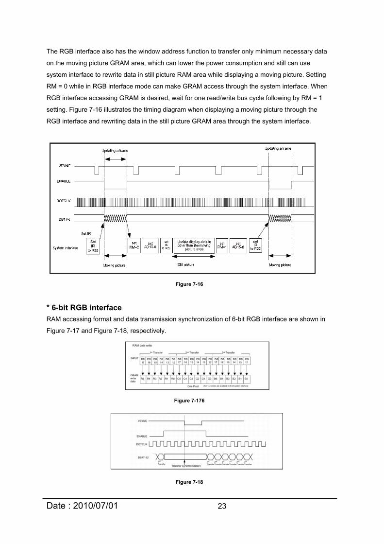
The RGB interface also has the window address function to transfer only minimum necessary data
on the moving picture GRAM area, which can lower the power consumption and still can use
system interface to rewrite data in still picture RAM area while displaying a moving picture. Setting
RM = 0 while in RGB interface mode can make GRAM access through the system interface. When
RGB interface accessing GRAM is desired, wait for one read/write bus cycle following by RM = 1
setting. Figure 7-16 illustrates the timing diagram when displaying a moving picture through the
RGB interface and rewriting data in the still picture GRAM area through the system interface.
Figure 7-16
* 6-bit RGB interface RAM accessing format and data transmission synchronization of 6-bit RGB interface are shown in
Figure 7-17 and Figure 7-18, respectively.
Figure 7-176
Figure 7-18

Date : 2010/07/01 24
* 16-bit RGB interface
RAM accessing format of 16-bit RGB interface are shown in Figure 7-19.
Figure 7-19
* 18-bit RGB interface
RAM accessing format of 18-bit RGB interface are shown in Figure 8-21.
Figure 7-20

Preliminary The contents of this document are confidential and must not be disclosed wholly or in part to any third part without the prior written consent of AMPIRE CO., LTD
Date : 2010/07/01 25
7-7 Instruction List Main LCD Driver IC:RM68050

Preliminary The contents of this document are confidential and must not be disclosed wholly or in part to any third part without the prior written consent of AMPIRE CO., LTD
Date : 2010/07/01 26
8 Application 8-1 Display ON / OFF
Preliminary The contents of this document are confidential and must not be disclosed wholly or in part to any third part without the prior written consent of AMPIRE CO., LTD
Date : 2010/07/01 27
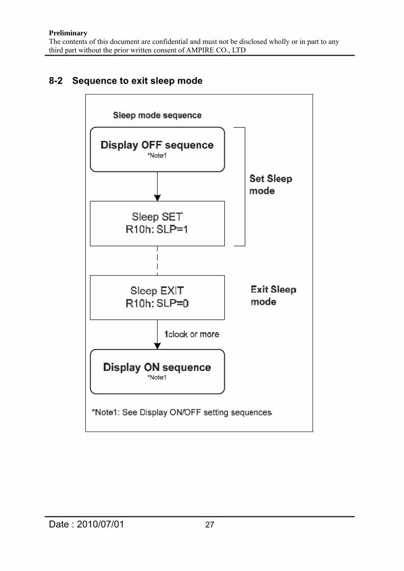
8-2 Sequence to exit sleep mode

Preliminary The contents of this document are confidential and must not be disclosed wholly or in part to any third part without the prior written consent of AMPIRE CO., LTD
Date : 2010/07/01 28
8-3 Power Supply Configuration
Power Supply ON/OFF Sequence

Preliminary The contents of this document are confidential and must not be disclosed wholly or in part to any third part without the prior written consent of AMPIRE CO., LTD
Date : 2010/07/01 29
9 Electrical Characteristics

Preliminary The contents of this document are confidential and must not be disclosed wholly or in part to any third part without the prior written consent of AMPIRE CO., LTD
Date : 2010/07/01 30

Preliminary The contents of this document are confidential and must not be disclosed wholly or in part to any third part without the prior written consent of AMPIRE CO., LTD
Date : 2010/07/01 31

Preliminary The contents of this document are confidential and must not be disclosed wholly or in part to any third part without the prior written consent of AMPIRE CO., LTD
Date : 2010/07/01 . 32
10 QUALITY AND RELIABILITY
10-1 TEST CONDITIONS Tests should be conducted under the following conditions : Ambient temperature : 25 ± 5°C Humidity : 60 ± 25% RH. 10-2 SAMPLING PLAN
Sampling method shall be in accordance with MIL-STD-105E , level II, normal single sampling plan . 10-3 ACCEPTABLE QUALITY LEVEL
A major defect is defined as one that could cause failure to or materially reduce the usability of the unit for its intended purpose. A minor defect is one that does not materially reduce the usability of the unit for its intended purpose or is an infringement from established standards and has no significant bearing on its effective use or operation. 10-4 APPEARANCE An appearance test should be conducted by human sight at approximately 30 cm distance from the LCD module under florescent light. The inspection area of LCD panel shall be within the range of following limits.

Preliminary The contents of this document are confidential and must not be disclosed wholly or in part to any third part without the prior written consent of AMPIRE CO., LTD
Date : 2010/07/01 33
10-5 INSPECTION QUALITY CRITERIA
No. Item Criterion for defects Class
of Defec
Acceptable level
1 Non display No non display is allowed Major 0.65
2 Scratch,Dent of Plastic Mold Serious one is not allowed Major 0.65
3 Scratch on FPC By limited sample Major 0.65
4 Dot Defect
Minor 1.5
5 Line Defect None Minor 1.5
6 Uneven Brightness : Line Shape None Major 0.65
7 Uneven Brightness : Dot Shape None Major 0.65
8 Display pattern Unit:mm
0.302
BA≤
+ 0 < C 0.252
ED≤
+0.25
2F
≤+ G
Note: 1. Acceptable up to 3 damages 2. NG if there’re to two or more pinholes per dot
Minor 1.5
9
Scratch of Polarizer :Dot Shape s
Size:
2BAD +
=
Size D (mm) Acceptable number D < 0.1
0.1 < D < 0.3 0.3 < D
Ignore 3 0
Minor 1.5

Preliminary The contents of this document are confidential and must not be disclosed wholly or in part to any third part without the prior written consent of AMPIRE CO., LTD
Date : 2010/07/01 34
10
Scratch of Polarizer :
Line Shape
Width (mm) Length (mm) Acceptable number W<0.05
0.1<W<0.05 0.1<W
L < 0.3
0.3 < L < 2.0
-
Ignore
See dot shape
Minor 1.5
11 Bubble in polarizer
Size D (mm) Acceptable number D < 0.3
0.30 < D < 0.50 0.50 < D
Ignore 1 0
Minor 1.5
12 Stains inclusion : Line shape
Width (mm) Length (mm) Acceptable number W<0.04
0.04<W<0.06 0.06<W
Ignore L < 0.8
-
Not Allowed Not Allowed Not Allowed
Minor 1.5
13 Stains inclusion : dot shape
Size D (mm) Acceptable number D < 0.1
0.1 < D < 0.2 0.25< D
Not Allowed Not Allowed Not Allowed
Minor 1.5
14 Newton Ring
(A). The lightness of environment is 500 Lux
(B). The distance between product and eye is about 30cm
(C). The angle of 60° between eye
(D). Please find data below for your reference
Not Allowed Newton Ring
Major 0.65

Preliminary The contents of this document are confidential and must not be disclosed wholly or in part to any third part without the prior written consent of AMPIRE CO., LTD
Date : 2010/07/01 35
10-6 RELIABILITY
Test Item Test Conditions NoteHigh Temperature Operation 70±3°C , t=72 hrs Low Temperature Operation -10±3°C , t=72 hrs High Temperature Storage 80±3°C , t=72hrs 1,2 Low Temperature Storage -30±3°C , t=72 hrs 1,2 Temperature /Humidity
Storage Test 60°C, Humidity 90%, 72 hrs 1,2
Temperature /Humidity Operation Test 40°C, Humidity 90%, 72 hrs 1,2
Thermal Shock Test -20°C ~ 70°C
60 min 60 min. ( 1 cycle ) Total 20 cycle
1,2
Vibration Test (Packing)
Sweep frequency:10~55~10 Hz/1min Amplitude : 0.75mm Test direction : X.Y.Z/3 axis Duration : 30min/each axis
2
Static Electricity 150pF 330 ohm +8kV, 10times air discharge +5kV, 10times contact discharge
Note 1 : Condensation of water is not permitted on the module. Note 2 : The module should be inspected after 1 hour storage in normal conditions (15-35°C , 45-65%RH). Definitions of life end point :
Current drain should be smaller than the specific value. Function of the module should be maintained. Appearance and display quality should not have degraded noticeably. Contrast ratio should be greater than 50% of the initial value.

Preliminary The contents of this document are confidential and must not be disclosed wholly or in part to any third part without the prior written consent of AMPIRE CO., LTD
Date : 2010/07/01 36
11 USE PRECAUTIONS
11-1 Handling precautions
1) The polarizing plate may break easily so be careful when handling it. Do not touch, press or rub it with a hard-material tool like tweezers.
2) Do not touch the polarizing plate surface with bare hands so as not to make it dirty. If the surface or other related part of the polarizing plate is dirty, soak a soft cotton cloth or chamois leather in benzine and wipe off with it. Do not use chemical liquids such as acetone, toluene and isopropyl alcohol. Failure to do so may bring chemical reaction phenomena and deteriorations.
3) Remove any spit or water immediately. If it is left for hours, the suffered part may deform or decolorize.
4) If the LCD element breaks and any LC stuff leaks, do not suck or lick it. Also if LC stuff is stuck on your skin or clothing, wash thoroughly with soap and water immediately.
11-2 Installing precautions
1) The PCB has many ICs that may be damaged easily by static electricity. To prevent breaking by static electricity from the human body and clothing, earth the human body properly using the high resistance and discharge static electricity during the operation. In this case, however, the resistance value should be approx. 1MΩ and the resistance should be placed near the human body rather than the ground surface. When the indoor space is dry, static electricity may occur easily so be careful. We recommend the indoor space should be kept with humidity of 60% or more. When a soldering iron or other similar tool is used for assembly, be sure to earth it.
2) When installing the module and ICs, do not bend or twist them. Failure to do so may crack LC element and cause circuit failure.
3) To protect LC element, especially polarizing plate, use a transparent protective plate (e.g., acrylic plate, glass etc) for the product case.
4) Do not use an adhesive like a both-side adhesive tape to make LCD surface (polarizing plate) and product case stick together. Failure to do so may cause the polarizing plate to peel off.

Preliminary The contents of this document are confidential and must not be disclosed wholly or in part to any third part without the prior written consent of AMPIRE CO., LTD
Date : 2010/07/01 37
11-3 Storage precautions
1) Avoid a high temperature and humidity area. Keep the temperature between 0°C and 35°C and also the humidity under 60%.
2) Choose the dark spaces where the product is not exposed to direct sunlight or fluorescent light.
3) Store the products as they are put in the boxes provided from us or in the same conditions as we recommend.
11-4 Operating precautions
1) Do not boost the applied drive voltage abnormally. Failure to do so may break ICs. When applying power voltage, check the electrical features beforehand and be careful. Always turn off the power to the LC module controller before removing or inserting the LC module input connector. If the input connector is removed or inserted while the power is turned on, the LC module internal circuit may break.
2) The display response may be late if the operating temperature is under the normal standard, and the display may be out of order if it is above the normal standard. But this is not a failure; this will be restored if it is within the normal standard.
3) The LCD contrast varies depending on the visual angle, ambient temperature, power voltage etc. Obtain the optimum contrast by adjusting the LC dive voltage.
4) When carrying out the test, do not take the module out of the low-temperature space suddenly. Failure to do so will cause the module condensing, leading to malfunctions.
5) Make certain that each signal noise level is within the standard (L level: 0.2Vdd or less and H level: 0.8Vdd or more) even if the module has functioned properly. If it is beyond the standard, the module may often malfunction. In addition, always connect the module when making noise level measurements.
6) The CMOS ICs are incorporated in the module and the pull-up and pull-down function is not adopted for the input so avoid putting the input signal open while the power is ON.
7) The characteristic of the semiconductor element changes when it is exposed to light emissions, therefore ICs on the LCD may malfunction if they receive light

Preliminary The contents of this document are confidential and must not be disclosed wholly or in part to any third part without the prior written consent of AMPIRE CO., LTD
Date : 2010/07/01 38
emissions. To prevent these malfunctions, design and assemble ICs so that they are shielded from light emissions.
8) Crosstalk occurs because of characteristics of the LCD. In general, crosstalk occurs when the regularized display is maintained. Also, crosstalk is affected by the LC drive voltage. Design the contents of the display, considering crosstalk.
11-5 Other
1) Do not disassemble or take the LC module into pieces. The LC modules once disassembled or taken into pieces are not the guarantee articles.
2) The residual image may exist if the same display pattern is shown for hours. This residual image, however, disappears when another display pattern is shown or the drive is interrupted and left for a while. But this is not a problem on reliability.
3) AMIPRE will provide one years warrantee for all products and three months warrantee for all repairing products.

Preliminary The contents of this document are confidential and must not be disclosed wholly or in part to any third part without the prior written consent of AMPIRE CO., LTD
Date : 2010/07/01 39
12 MECHANICAL DRAWING

科技
光晶
采電
*真空
盒交
錯堆
疊
Preliminary The contents of this document are confidential and must not be disclosed wholly or in part to any third part without the prior written consent of AMPIRE CO., LTD
Date : 2010/07/01 39
Recommended