ARM7 Microprocessor
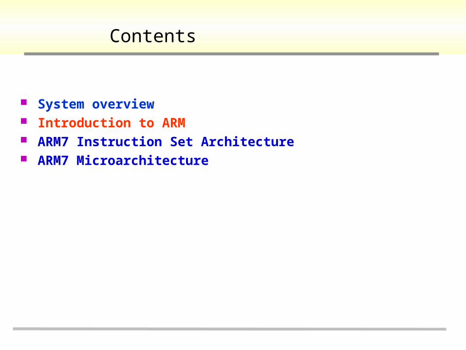
Contents
System overview Introduction to ARM ARM7 Instruction Set Architecture ARM7 Microarchitecture
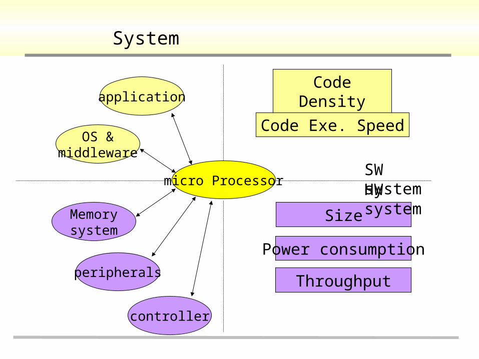
System
micro Processor
application
OS &middleware
Memorysystem
peripherals
controller
Code Density
Code Exe. Speed
Size
Power consumption
Throughput
SW systemHW system
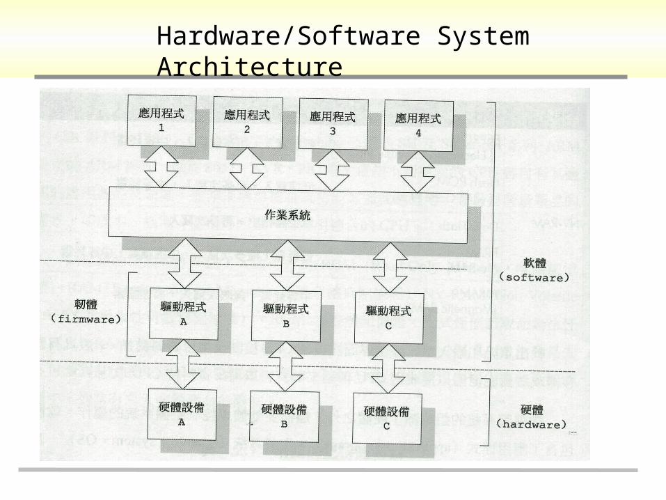
Hardware/Software System Architecture
Microprocessor
Factors in deciding processor architecture for a system Operating environment
General purpose system Special / limited purpose system (embedded system)
Required performance Is high throughput required? (e.g. clock speed, pipeline depth) Is optimized functionalities required? (e.g. communication) Is power consumption control critical?
Tradeoffs High performance = high power Many functionalities = high power & size
Microprocessor(cont’d)
High performance, general purpose Microprocessor Processor Architecture & Performance
General purpose processors Very high performance (e.g. throughput, clock speed, etc.) Provide various functionalities (e.g. multimedia instruction set) High throughput at cost of high power
Software vs. Hardware Implementation overhead is in software Software optimization is not critical
Examples Intel Pentium class AMD processors
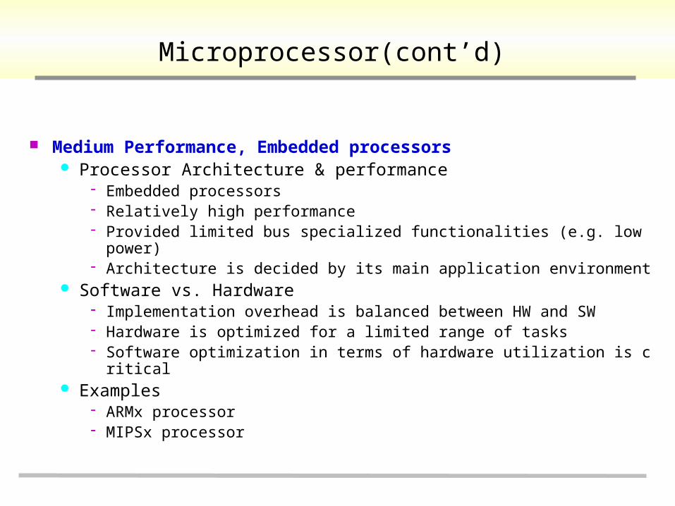
Microprocessor(cont’d)
Medium Performance, Embedded processors Processor Architecture & performance
Embedded processors Relatively high performance Provided limited bus specialized functionalities (e.g. low power) Architecture is decided by its main application environment
Software vs. Hardware Implementation overhead is balanced between HW and SW Hardware is optimized for a limited range of tasks Software optimization in terms of hardware utilization is critical
Examples ARMx processor MIPSx processor
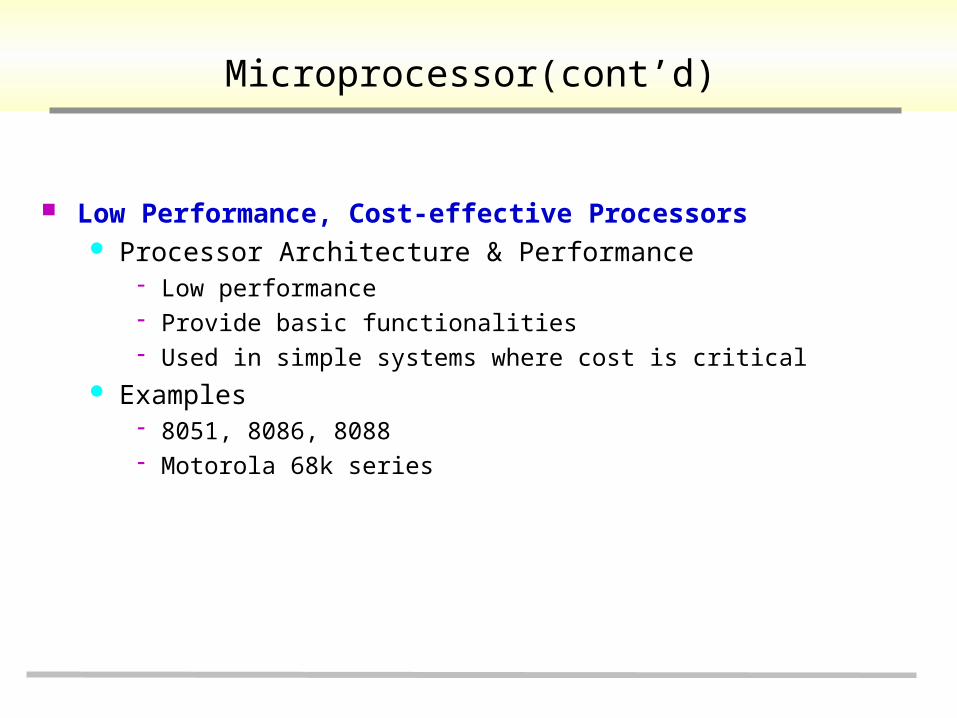
Microprocessor(cont’d)
Low Performance, Cost-effective Processors Processor Architecture & Performance
Low performance Provide basic functionalities Used in simple systems where cost is critical
Examples 8051, 8086, 8088 Motorola 68k series
Contents
System overview Introduction to ARM ARM7 Instruction Set Architecture ARM7 Microarchitecture
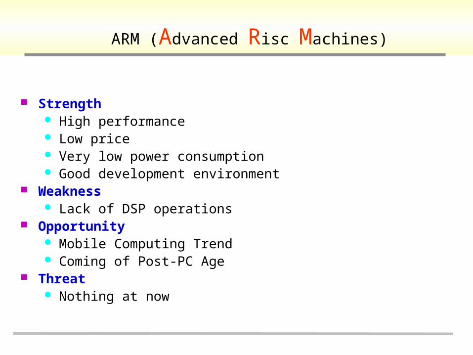
ARM (Advanced Risc Machines)
Strength High performance Low price Very low power consumption Good development environment
Weakness Lack of DSP operations
Opportunity Mobile Computing Trend Coming of Post-PC Age
Threat Nothing at now
Contents
System overview Introduction to ARM ARM7 Instruction Set Architecture ARM7 Microarchitecture
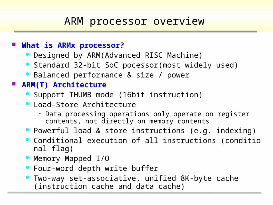
ARM processor overview
What is ARMx processor? Designed by ARM(Advanced RISC Machine) Standard 32-bit SoC pocessor(most widely used) Balanced performance & size / power
ARM(T) Architecture Support THUMB mode (16bit instruction) Load-Store Architecture
Data processing operations only operate on register contents, not directly on memory contents
Powerful load & store instructions (e.g. indexing) Conditional execution of all instructions (conditional flag) Memory Mapped I/O Four-word depth write buffer Two-way set-associative, unified 8K-byte cache (instruction cache
and data cache)
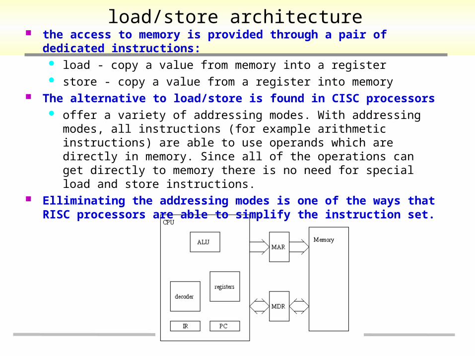
load/store architecture the access to memory is provided through a pair of dedicated
instructions: load - copy a value from memory into a register store - copy a value from a register into memory
The alternative to load/store is found in CISC processors offer a variety of addressing modes. With addressing modes, all
instructions (for example arithmetic instructions) are able to use operands which are directly in memory. Since all of the operations can get directly to memory there is no need for special load and store instructions.
Elliminating the addressing modes is one of the ways that RISC processors are able to simplify the instruction set.
ARM7 Programmer’s model
Overview Operational Modes Exceptions
Overview
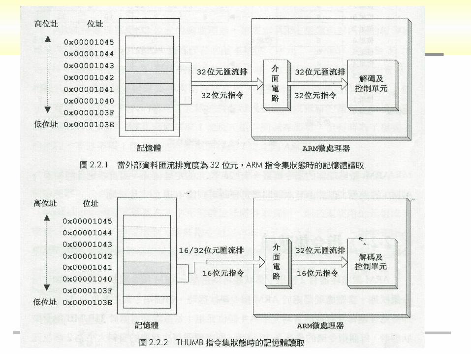
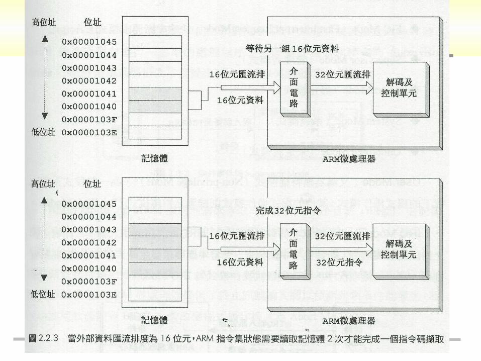
From the programmer’s point of view, the ARM can be in one of two states Normal state: execute 32-bit, word-aligned ARM instructions THUMB state: operate with 16-bit, half-word-aligned THUMB
instructions Transition between these two states does not affect the processor
mode or the contents of the registers THUMB instructions are one-half the bit width of normal ARM
instructions Produce very high-density codes If the memory bus width is 16-bit or 8-bit, the THUMB instruction will
be has a good performance than normal instruction sets
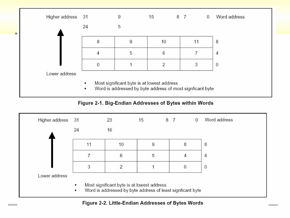
Overview Memory formats
View memory as a linear collection of bytes numbered upwards from zero
Bytes 0 to 3 hold the first stored word, bytes 4 to 7 the second and so on.
Can treat words in memory as being stored either in Big-Endian or Little-Endian format Big-Endian format : the most significant byte of a word is stored at
the lowest numbered byte and the least significant byte at the highest numbered byte (byte 0 of the memory system is therefore connected to data lines 31 through 24)
Little-Endian format: the lowest numbered byte in a word is considered the word’s least significant byte, and the highest numbered byte the most significant. (byte 0 of the memory system is therefore connected to data lines 7 through 0)
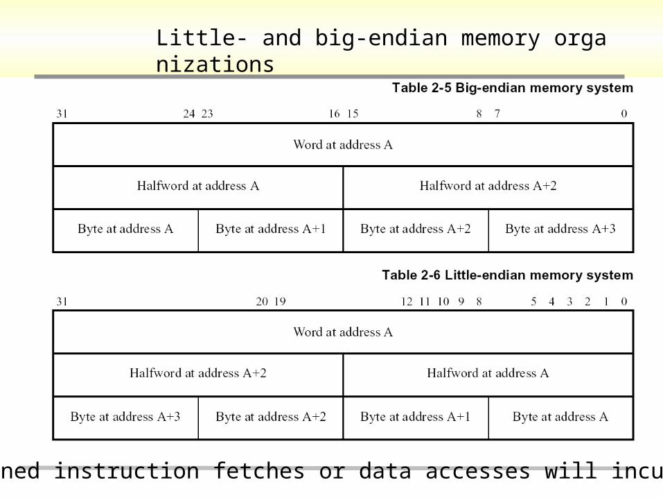
Little- and big-endian memory organizations
If unaligned instruction fetches or data accesses will incur errors
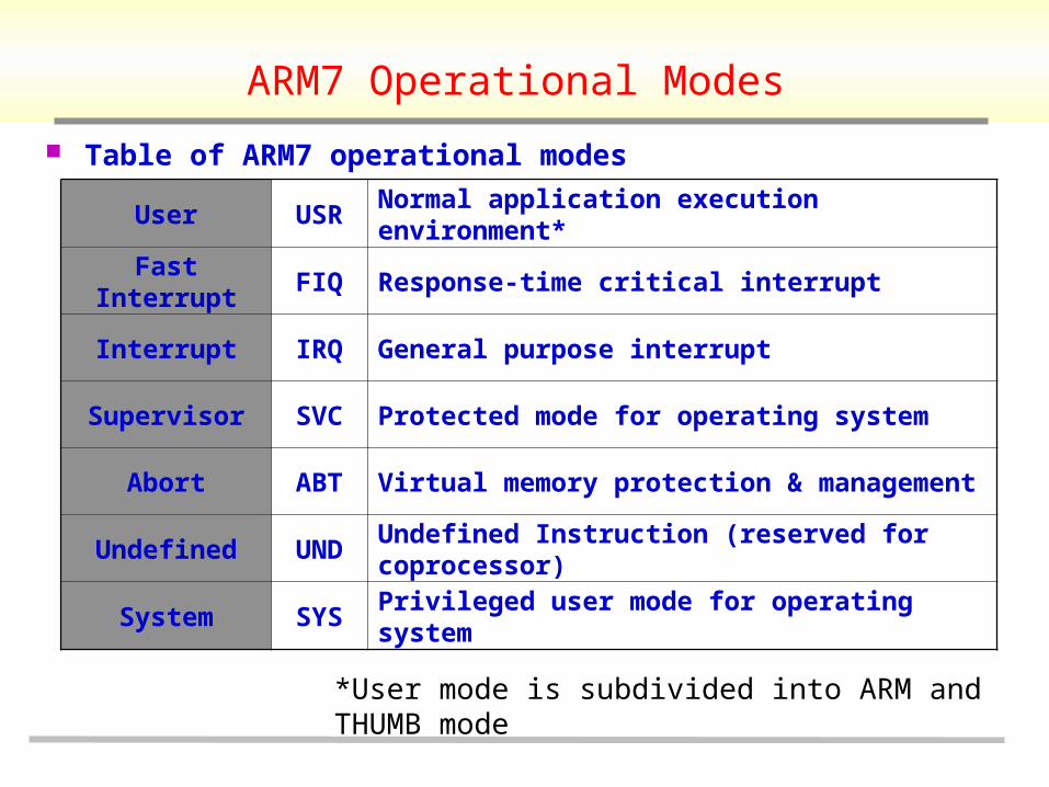
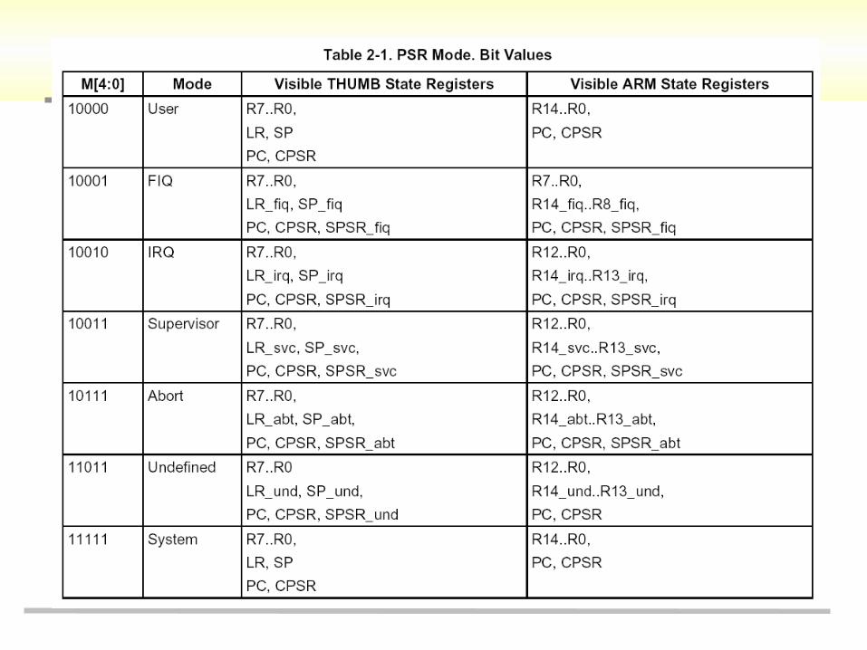
ARM7 Operational Modes
Table of ARM7 operational modes
User USR Normal application execution environment*
Fast Interrupt FIQ Response-time critical interrupt
Interrupt IRQ General purpose interrupt
Supervisor SVC Protected mode for operating system
Abort ABT Virtual memory protection & management
Undefined UNDUndefined Instruction (reserved for coprocessor)
System SYS Privileged user mode for operating system
*User mode is subdivided into ARM and THUMB mode
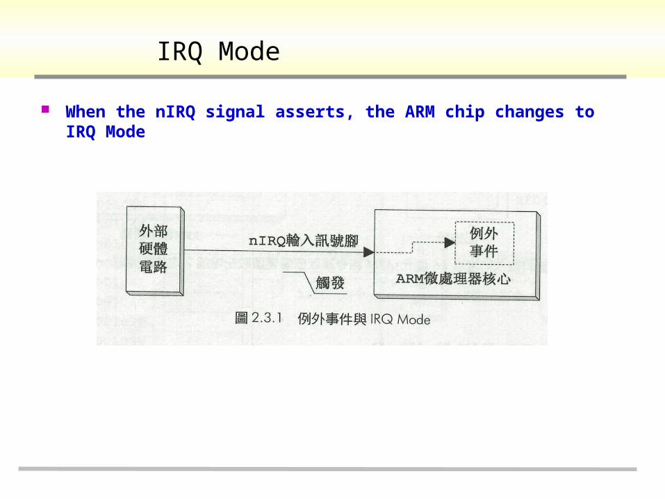
IRQ Mode
When the nIRQ signal asserts, the ARM chip changes to IRQ Mode
FIQ Mode
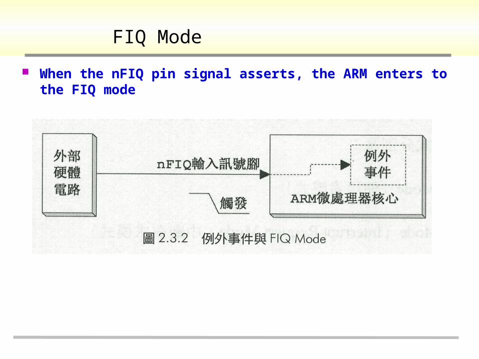
When the nFIQ pin signal asserts, the ARM enters to the FIQ mode
Supervisor mode
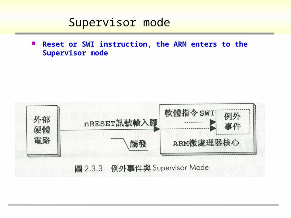
Reset or SWI instruction, the ARM enters to the Supervisor mode
Abort Mode
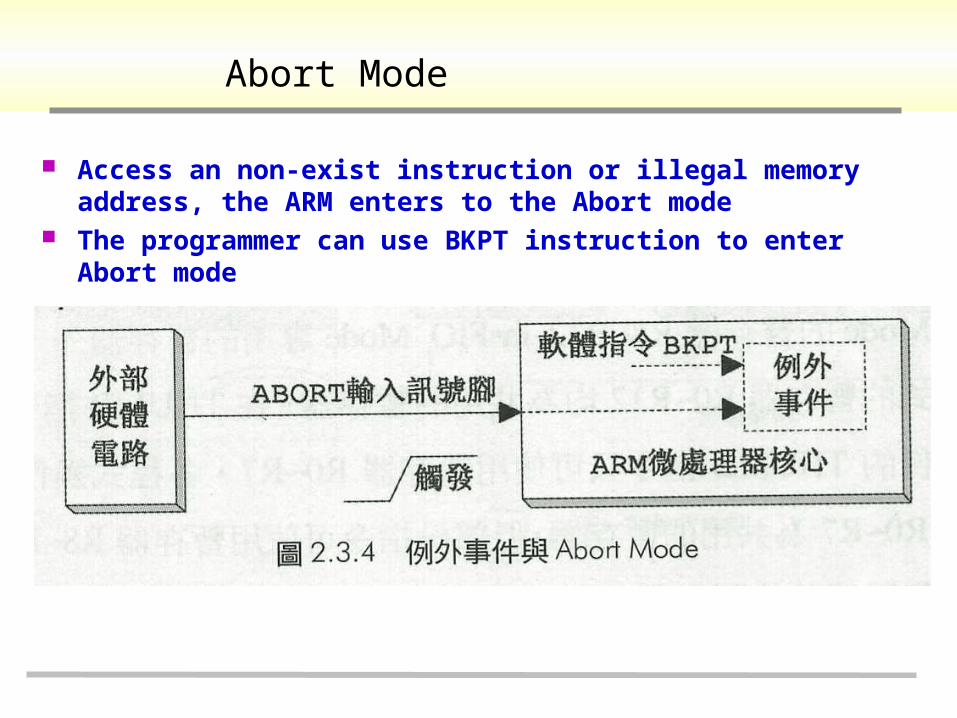
Access an non-exist instruction or illegal memory address, the ARM enters to the Abort mode
The programmer can use BKPT instruction to enter Abort mode
System mode and undefined mode
System mode It is not entered by any exception Intended for use by operating system tasks which need access to
system resources Use software to enter this mode
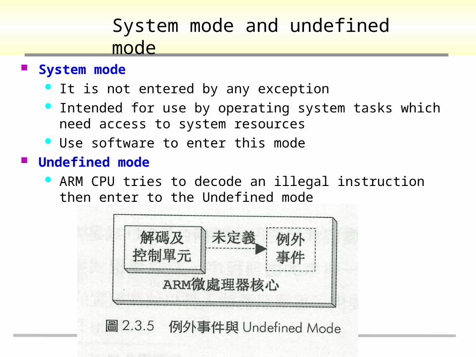
Undefined mode ARM CPU tries to decode an illegal instruction then enter to the
Undefined mode
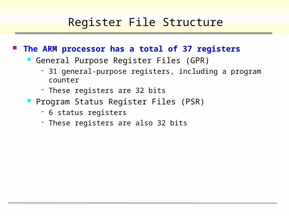
Register File Structure
The ARM processor has a total of 37 registers General Purpose Register Files (GPR)
31 general-purpose registers, including a program counter These registers are 32 bits
Program Status Register Files (PSR) 6 status registers These registers are also 32 bits
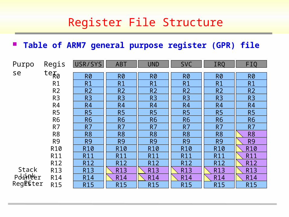
Register File Structure
Table of ARM7 general purpose register (GPR) file
Purpose Register USR/SYS
R0R1R2R3R4R5R6R7R8R9
R10R11R12R13R14R15
ABT
R0R1R2R3R4R5R6R7R8R9
R10R11R12R13R14R15
UND
R0R1R2R3R4R5R6R7R8R9
R10R11R12R13R14R15
SVC
R0R1R2R3R4R5R6R7R8R9
R10R11R12R13R14R15
IRQ
R0R1R2R3R4R5R6R7R8R9
R10R11R12R13R14R15
FIQ
R0R1R2R3R4R5R6R7R8R9
R10R11R12R13R14R15
Stack PointerLink Register
PC
R0R1R2R3R4R5R6R7R8R9
R10R11R12R13R14R15
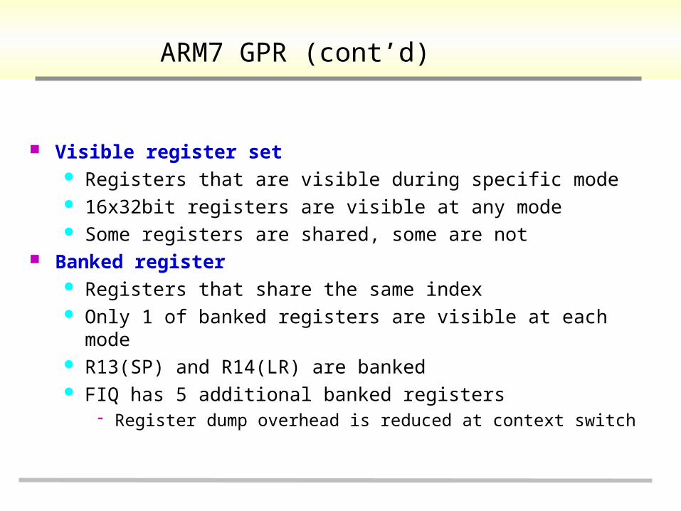
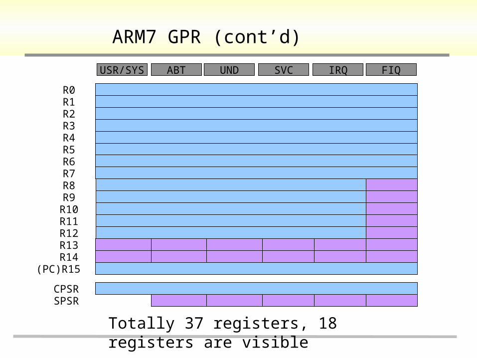
ARM7 GPR (cont’d)
Visible register set Registers that are visible during specific mode 16x32bit registers are visible at any mode Some registers are shared, some are not
Banked register Registers that share the same index Only 1 of banked registers are visible at each mode R13(SP) and R14(LR) are banked FIQ has 5 additional banked registers
Register dump overhead is reduced at context switch
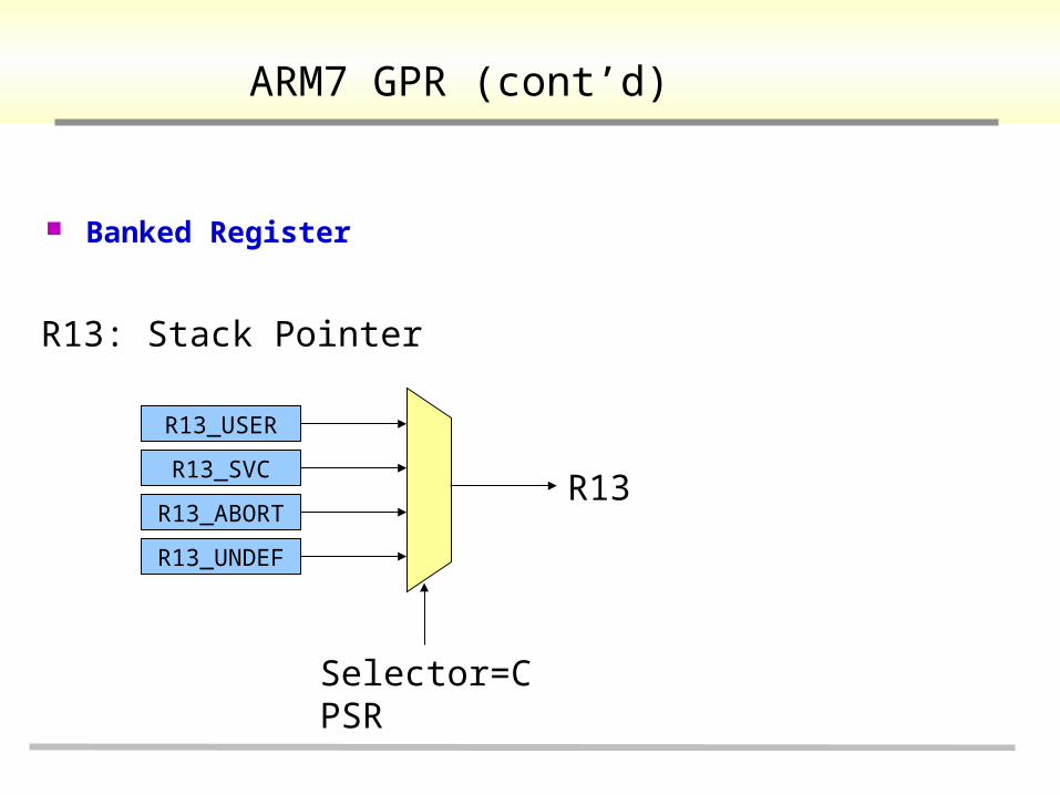
ARM7 GPR (cont’d)
Banked Register
R13_USER
R13_SVC
R13_ABORT
R13_UNDEF
R13
Selector=CPSR
R13: Stack Pointer
ARM7 GPR (cont’d)
USR/SYS ABT UND SVC IRQ FIQ
R0R1R2R3R4R5R6R7R8R9
R10R11R12R13R14
(PC)R15
CPSRSPSR
Totally 37 registers, 18 registers are visible
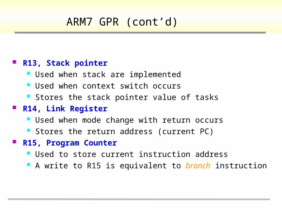
ARM7 GPR (cont’d)
R13, Stack pointer Used when stack are implemented Used when context switch occurs Stores the stack pointer value of tasks
R14, Link Register Used when mode change with return occurs Stores the return address (current PC)
R15, Program Counter Used to store current instruction address A write to R15 is equivalent to branch instruction
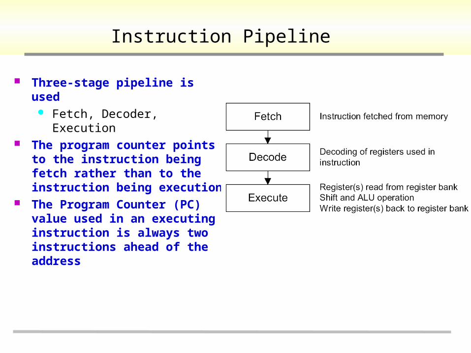
Instruction Pipeline
Three-stage pipeline is used Fetch, Decoder, Execution
The program counter points to the instruction being fetch rather than to the instruction being execution
The Program Counter (PC) value used in an executing instruction is always two instructions ahead of the address
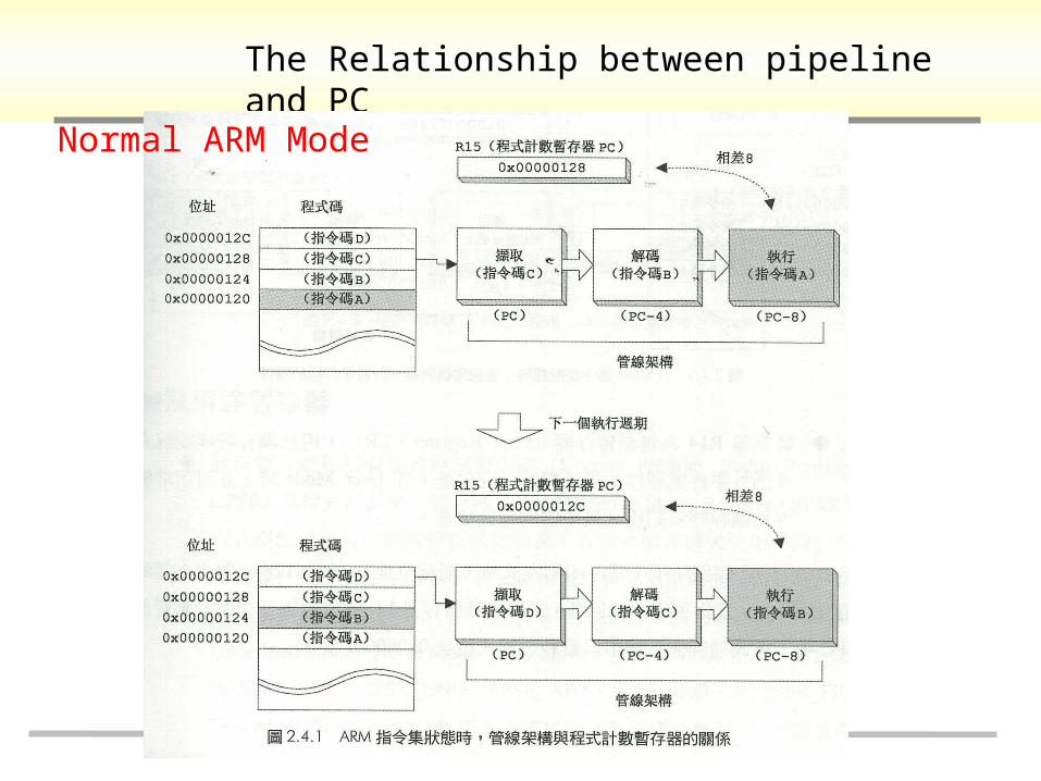
The Relationship between pipeline and PC
Normal ARM Mode
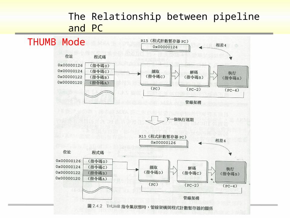
The Relationship between pipeline and PC
THUMB Mode
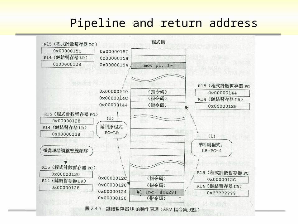
Pipeline and return address
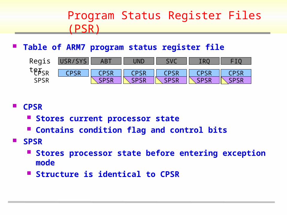
Program Status Register Files (PSR)
Table of ARM7 program status register file
CPSR Stores current processor state Contains condition flag and control bits
SPSR Stores processor state before entering exception mode Structure is identical to CPSR
Register USR/SYS ABT UND SVC IRQ FIQ
CPSRSPSR
CPSR CPSR CPSR CPSR CPSR CPSRSPSR SPSR SPSR SPSR SPSR
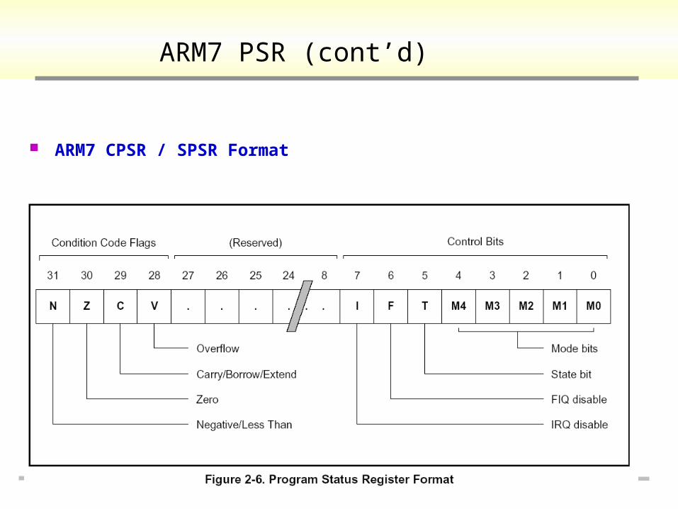
ARM7 PSR (cont’d)
ARM7 CPSR / SPSR Format
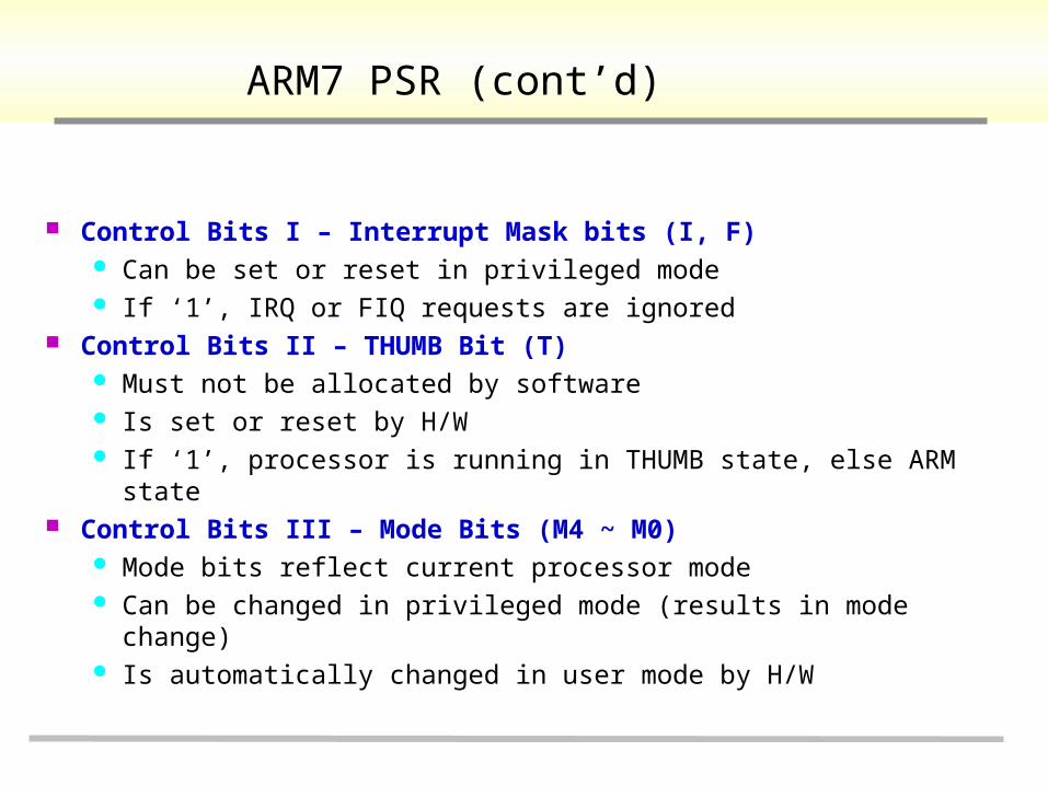
ARM7 PSR (cont’d)
Control Bits I – Interrupt Mask bits (I, F) Can be set or reset in privileged mode If ‘1’, IRQ or FIQ requests are ignored
Control Bits II – THUMB Bit (T) Must not be allocated by software Is set or reset by H/W If ‘1’, processor is running in THUMB state, else ARM state
Control Bits III – Mode Bits (M4 ~ M0) Mode bits reflect current processor mode Can be changed in privileged mode (results in mode change) Is automatically changed in user mode by H/W
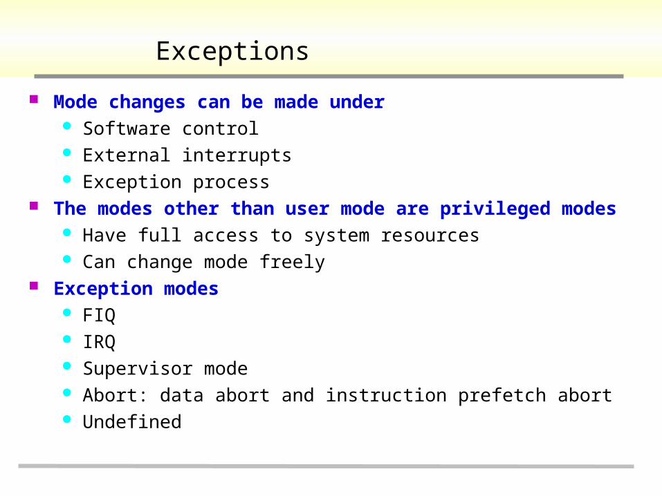
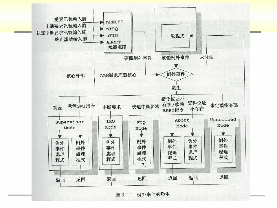
Exceptions
Mode changes can be made under Software control External interrupts Exception process
The modes other than user mode are privileged modes Have full access to system resources Can change mode freely
Exception modes FIQ IRQ Supervisor mode Abort: data abort and instruction prefetch abort Undefined
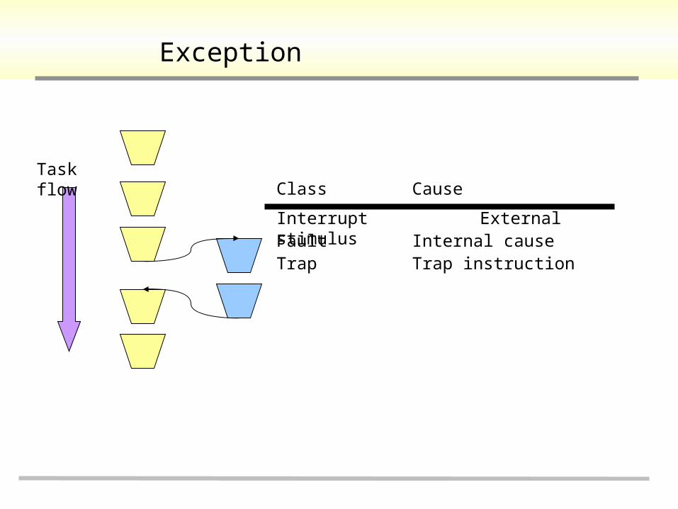
Exception
Task flowClass Cause
Interrupt External stimulusFault Internal causeTrap Trap instruction
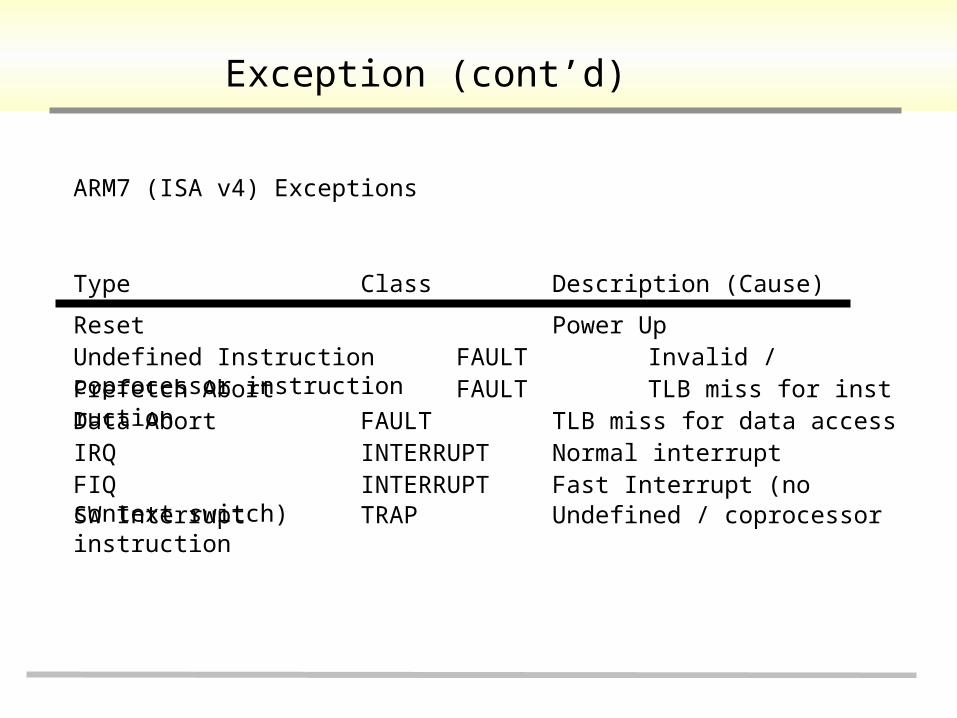
Exception (cont’d)
ARM7 (ISA v4) Exceptions
Type Class Description (Cause)
Reset Power UpUndefined Instruction FAULT Invalid / coprocessor instructionPrefetch Abort FAULT TLB miss for instructionData Abort FAULT TLB miss for data accessIRQ INTERRUPT Normal interruptFIQ INTERRUPT Fast Interrupt (no context switch)SW Interrupt TRAP Undefined / coprocessor instruction
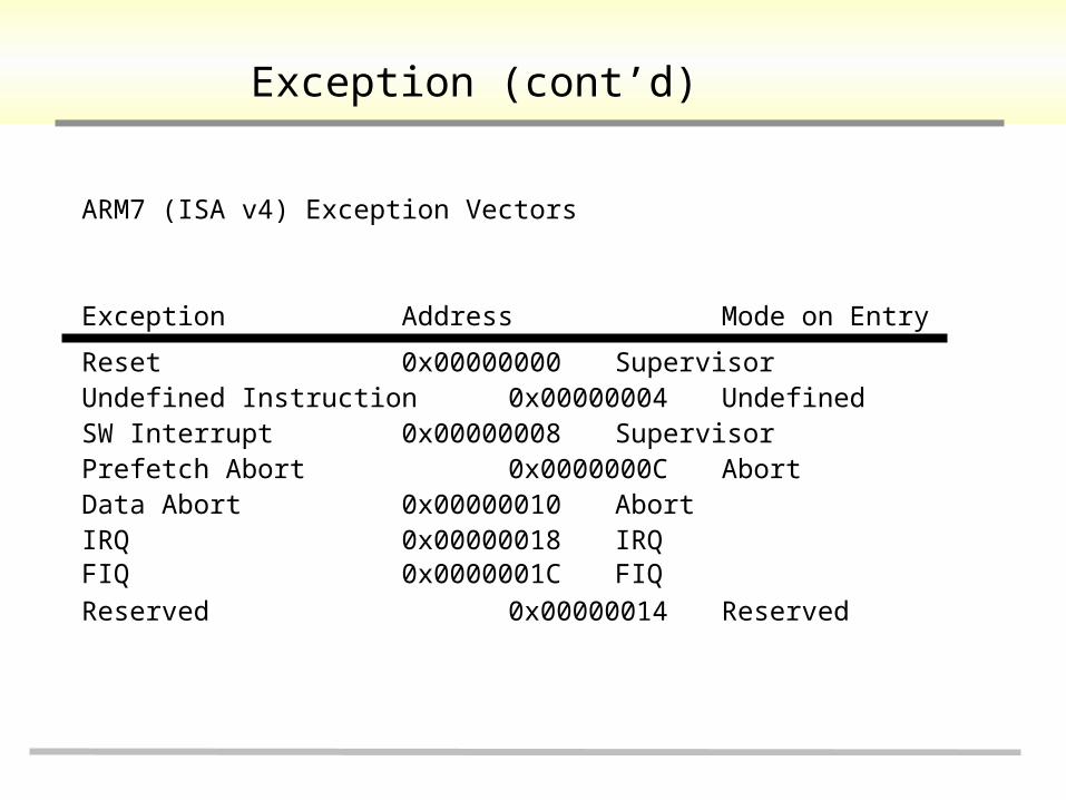
Exception (cont’d)
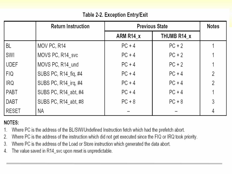
ARM7 (ISA v4) Exception Vectors
Exception Address Mode on Entry
Reset 0x00000000 SupervisorUndefined Instruction 0x00000004 UndefinedSW Interrupt 0x00000008 SupervisorPrefetch Abort 0x0000000C AbortData Abort 0x00000010 AbortIRQ 0x00000018 IRQFIQ 0x0000001C FIQ
Reserved 0x00000014 Reserved
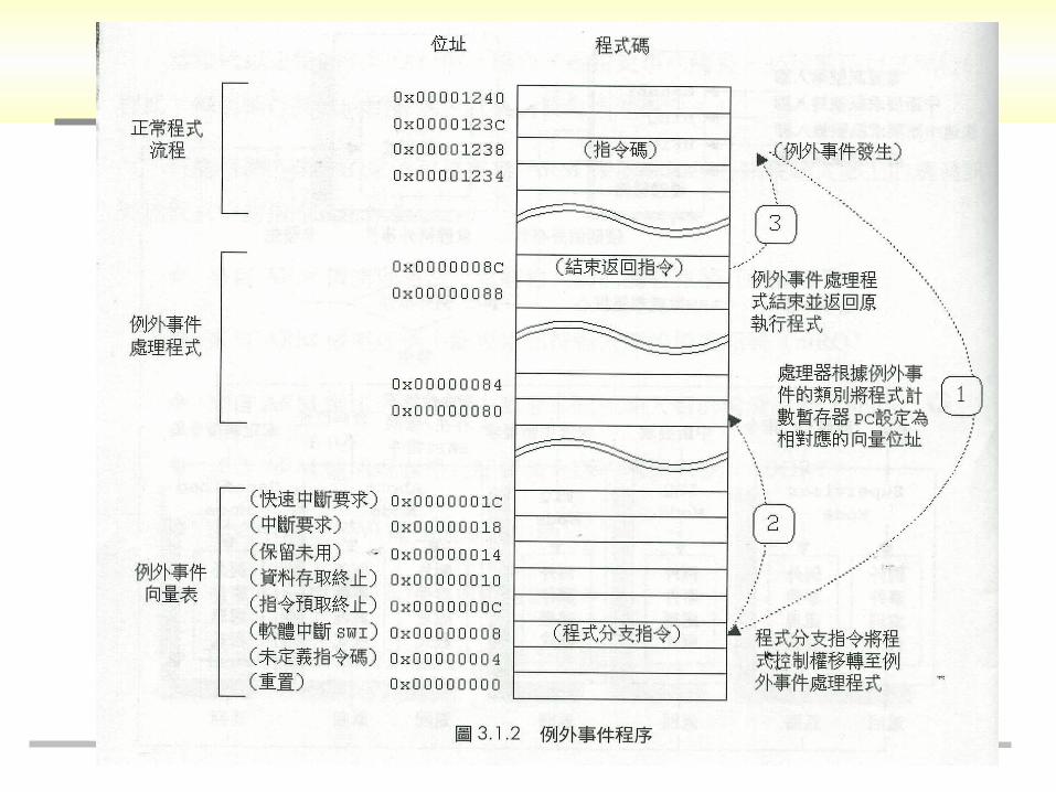
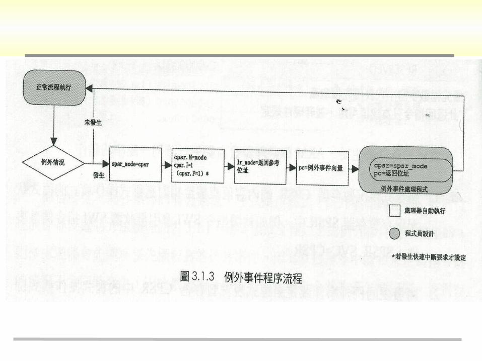
ARM Exceptions (cont’d)
On entry (automatically done by ARM) 1) completes the current instruction (except reset exception) 2) Changes to the operating mode corresponding to the 1) particular
exception 3) Saves the address of the following instruction in r14 of new mode 4) Saves the old value of the CPSR in the SPSR of the new mode 5) Disables IRQ exception; set bit 7 of the CPSR 6) If it a FIQ exception, disable further FIQ; disables bit 6 of the CPSR 7) Forces the PC to the address of exception handler
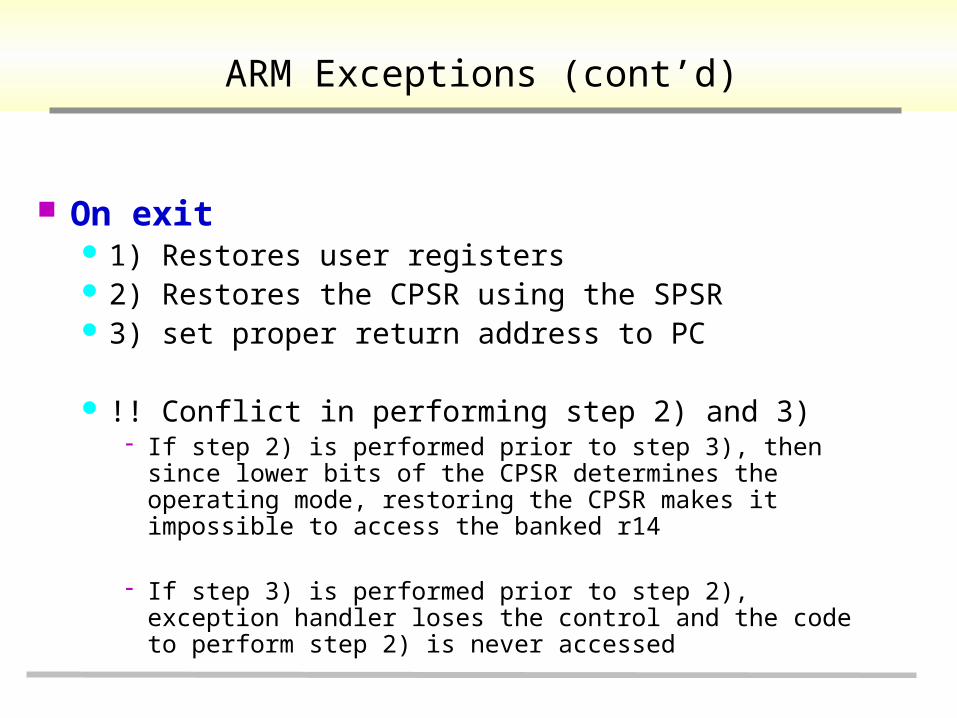
On exit 1) Restores user registers 2) Restores the CPSR using the SPSR 3) set proper return address to PC
!! Conflict in performing step 2) and 3) If step 2) is performed prior to step 3), then since lower bits
of the CPSR determines the operating mode, restoring the CPSR makes it impossible to access the banked r14
If step 3) is performed prior to step 2), exception handler loses the control and the code to perform step 2) is never accessed
ARM Exceptions (cont’d)
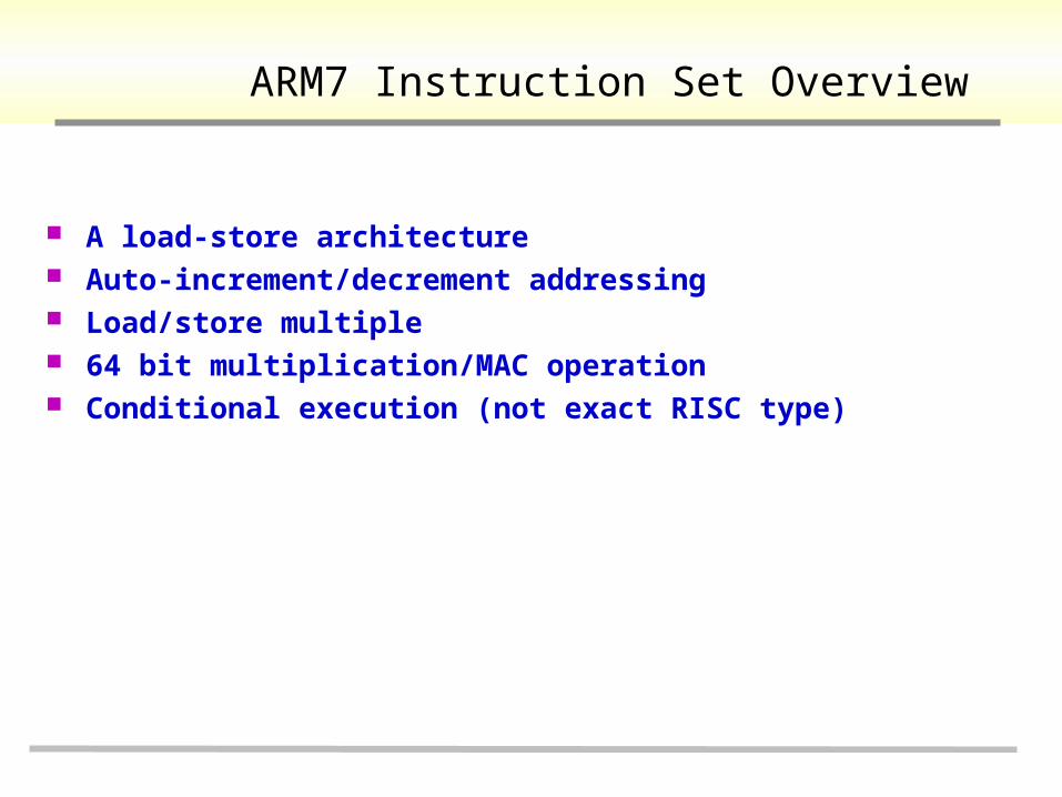
ARM7 Instruction Set Overview
A load-store architecture Auto-increment/decrement addressing Load/store multiple 64 bit multiplication/MAC operation Conditional execution (not exact RISC type)
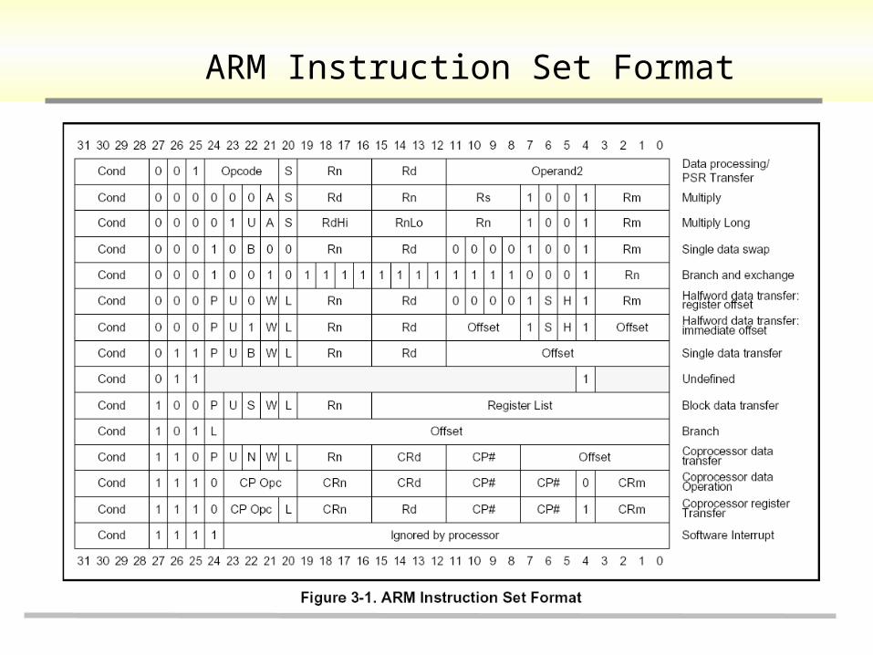
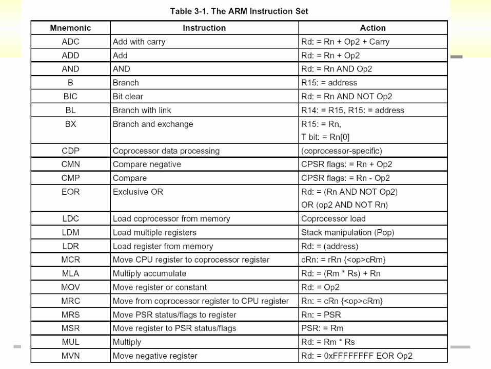
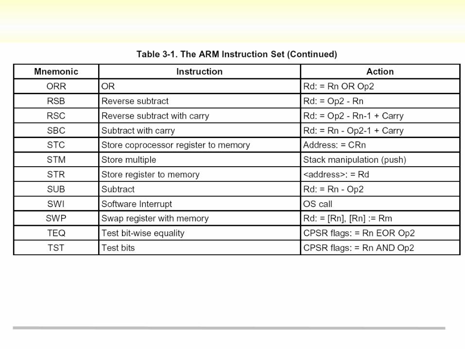
ARM Instruction Set Format
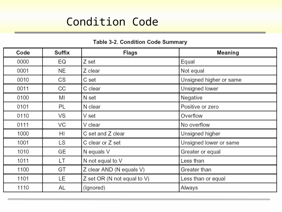
Condition Code
Contents
System overview Introduction to ARM ARM7 Instruction Set Architecture ARM7 Microarchitecture
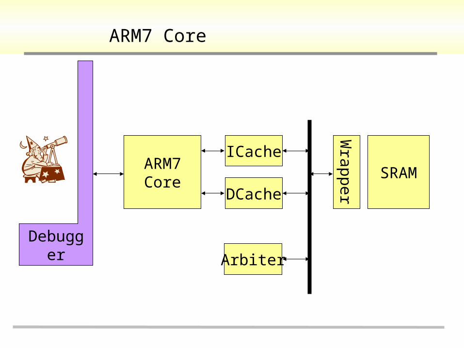
ARM7 Core
Debugger
ARM7Core
ICache
DCache
Arbiter
Wrapper
SRAM
ARM7 Datapath
ARM7 Datapath Pipeline Model Datapath Overview Clock Scheme IF Stage – Address MUX. & Incremental Block ID Stage – Register File EXE Stage
Overview of EXE Stage ALU Multiplier
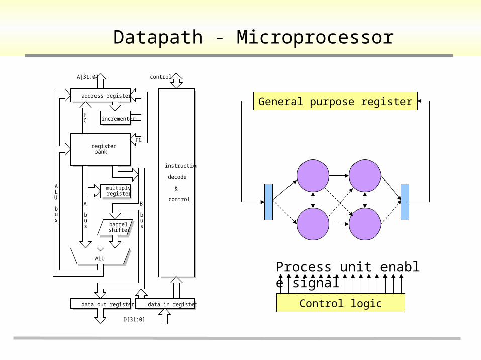
Datapath - Microprocessor
multiply
data out register
instruction
decode
&
control
incrementer
registerbank
address register
barrelshifter
A[31:0]
D[31:0]
data in register
ALU
control
PC
PC
ALU bus
A bus
B bus
register
General purpose register
Control logic
Process unit enable signal
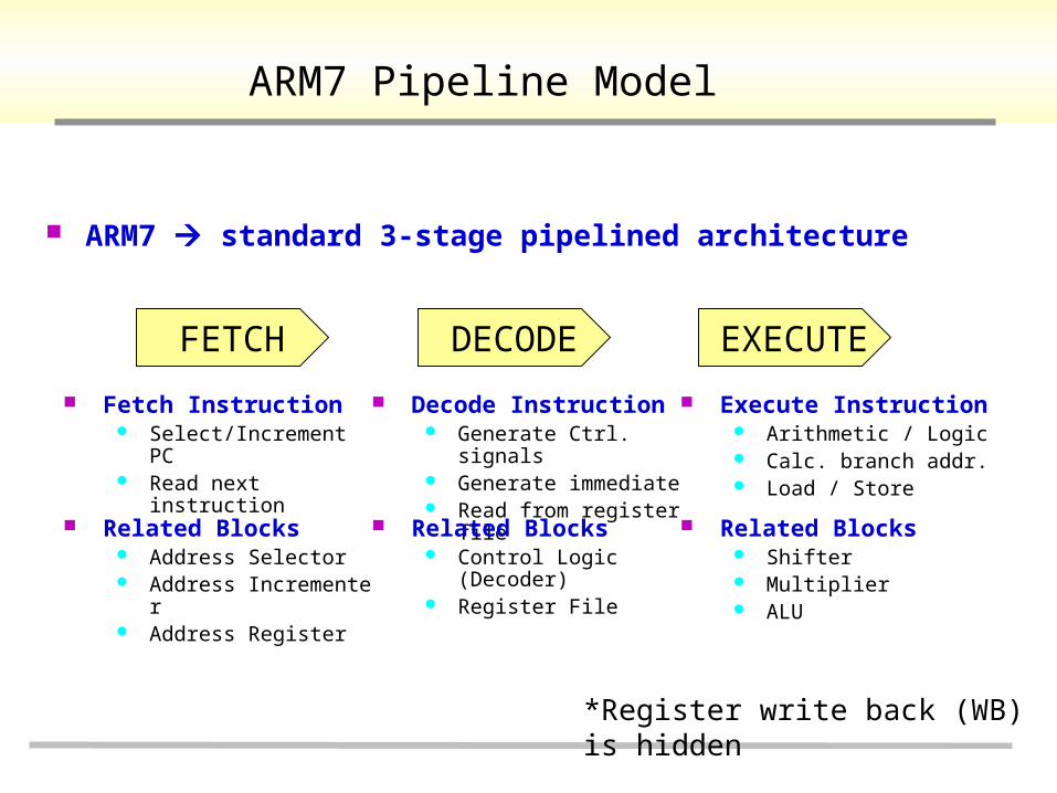
ARM7 Pipeline Model
ARM7 standard 3-stage pipelined architecture
FETCH DECODE EXECUTE
Fetch Instruction Select/Increment PC Read next instruction
Related Blocks Address Selector Address Incrementer Address Register
Decode Instruction Generate Ctrl. signals Generate immediate Read from register file
Related Blocks Control Logic (Decoder) Register File
Execute Instruction Arithmetic / Logic Calc. branch addr. Load / Store
Related Blocks Shifter Multiplier ALU
*Register write back (WB) is hidden
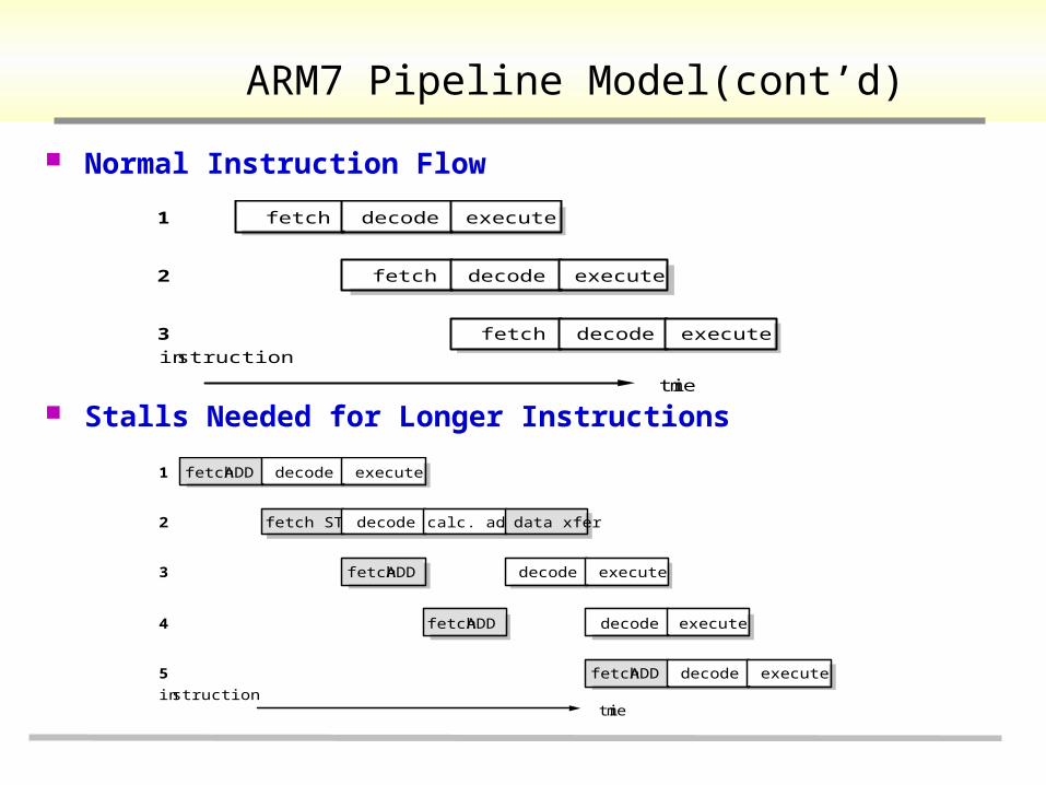
ARM7 Pipeline Model(cont’d)
Normal Instruction Flow
fetch decode execute
time
1
fetch decode execute
fetch decode execute
2
3
instruction
Stalls Needed for Longer Instructions
fetch ADD decode execute
time
1
fetch STR decode calc. addr.
fetch ADD decode execute
2
3
data xfer
fetch ADD decode execute4
5 fetch ADD decode execute
instruction
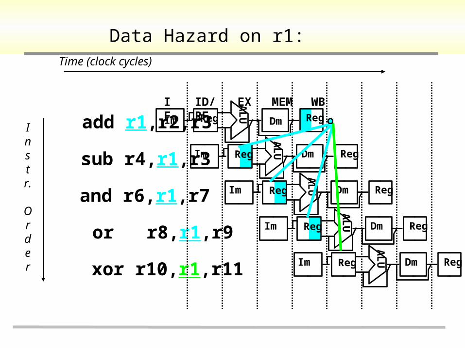
Data Hazard on r1:
Instr.
Order
Time (clock cycles)
add r1,r2,r3
sub r4,r1,r3
and r6,r1,r7
or r8,r1,r9
xor r10,r1,r11
IF ID/RF EX MEM WBALU
Im Reg Dm Reg
ALUIm Reg Dm Reg
ALUIm Reg Dm Reg
Im
ALUReg Dm Reg
ALUIm Reg Dm Reg
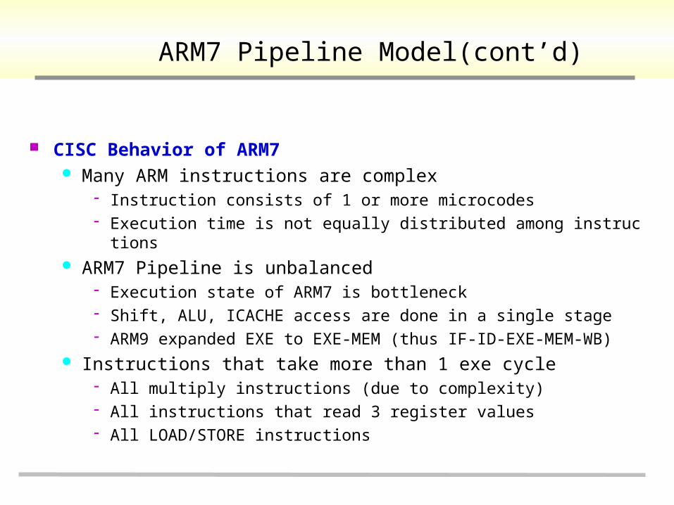
ARM7 Pipeline Model(cont’d)
CISC Behavior of ARM7 Many ARM instructions are complex
Instruction consists of 1 or more microcodes Execution time is not equally distributed among instructions
ARM7 Pipeline is unbalanced Execution state of ARM7 is bottleneck Shift, ALU, ICACHE access are done in a single stage ARM9 expanded EXE to EXE-MEM (thus IF-ID-EXE-MEM-WB)
Instructions that take more than 1 exe cycle All multiply instructions (due to complexity) All instructions that read 3 register values All LOAD/STORE instructions
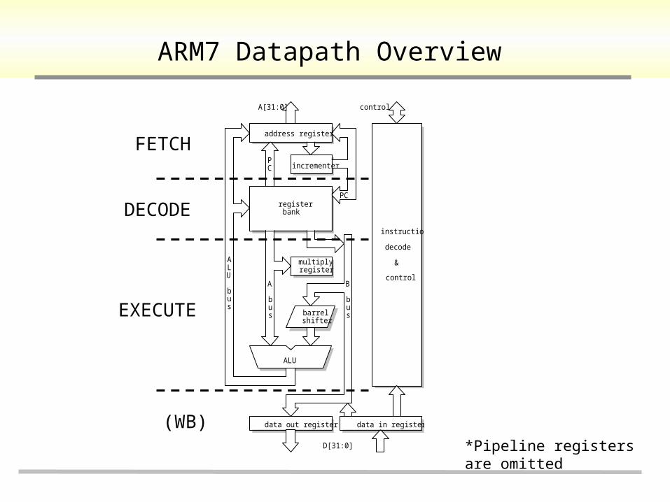
ARM7 Datapath Overview
multiply
data out register
instruction
decode
&
control
incrementer
registerbank
address register
barrelshifter
A[31:0]
D[31:0]
data in register
ALU
control
PC
PC
ALU bus
A bus
B bus
register
FETCH
DECODE
EXECUTE
(WB)*Pipeline registers are omitted
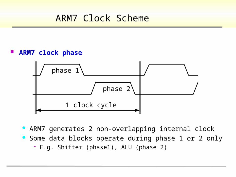
ARM7 Clock Scheme
ARM7 clock phase
ARM7 generates 2 non-overlapping internal clock Some data blocks operate during phase 1 or 2 only
E.g. Shifter (phase1), ALU (phase 2)
1 clock cycle
phase 1
phase 2
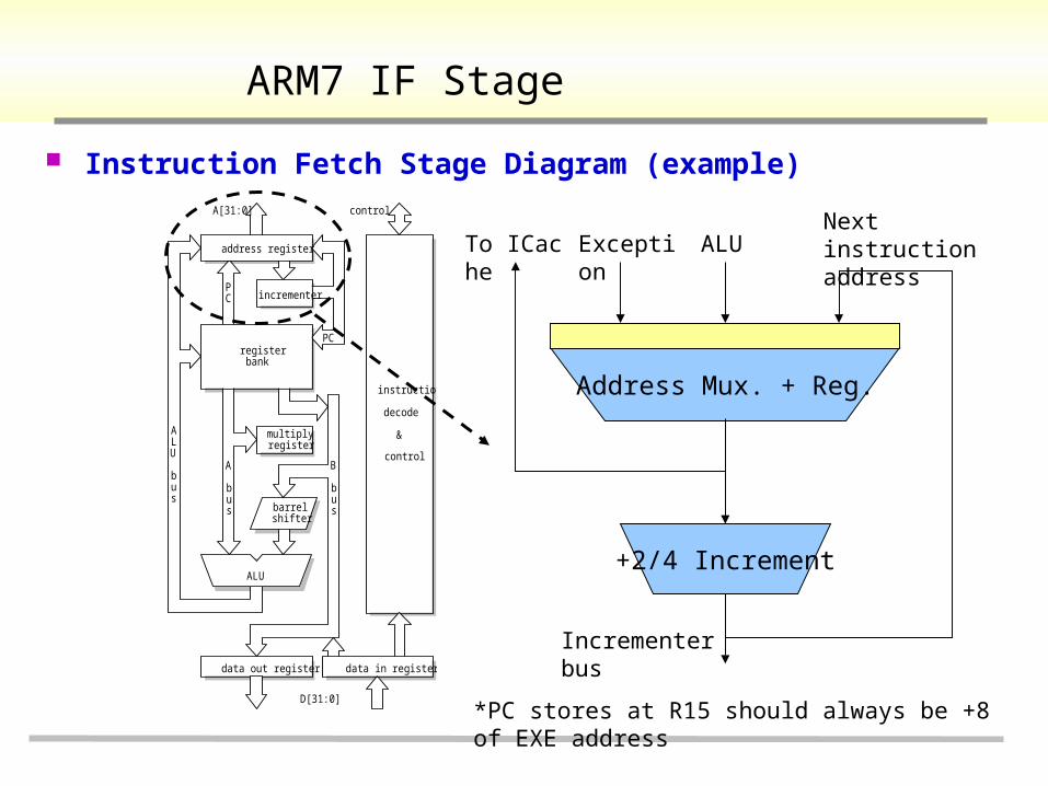
ARM7 IF Stage
multiply
data out register
instruction
decode
&
control
incrementer
registerbank
address register
barrelshifter
A[31:0]
D[31:0]
data in register
ALU
control
PC
PC
ALU bus
A bus
B bus
register
Instruction Fetch Stage Diagram (example)
Address Mux. + Reg.
+2/4 Increment
Incrementer bus
ALUNext instruction addressExceptionTo ICache
*PC stores at R15 should always be +8 of EXE address
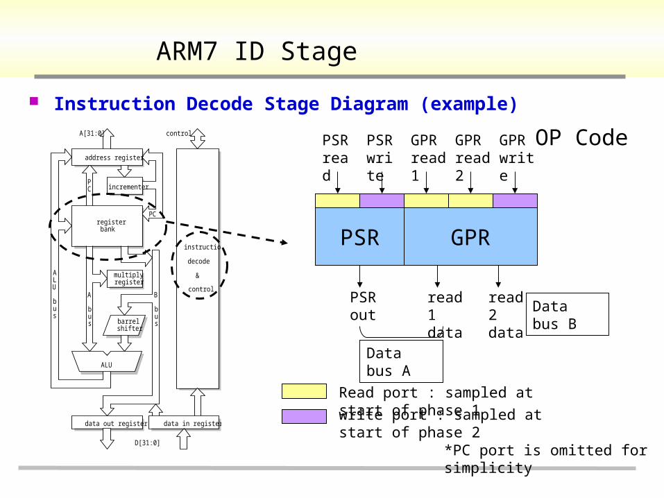
ARM7 ID Stage
Instruction Decode Stage Diagram (example)
multiply
data out register
instruction
decode
&
control
incrementer
registerbank
address register
barrelshifter
A[31:0]
D[31:0]
data in register
ALU
control
PC
PC
ALU bus
A bus
B bus
register
PSR GPR
PSR read
PSR write
GPR read1
GPR read2
GPR write
PSR out
read1 data
read2 data
Data bus A
Data bus B
Read port : sampled at start of phase 1
write port : sampled at start of phase 2
*PC port is omitted for simplicity
OP Code
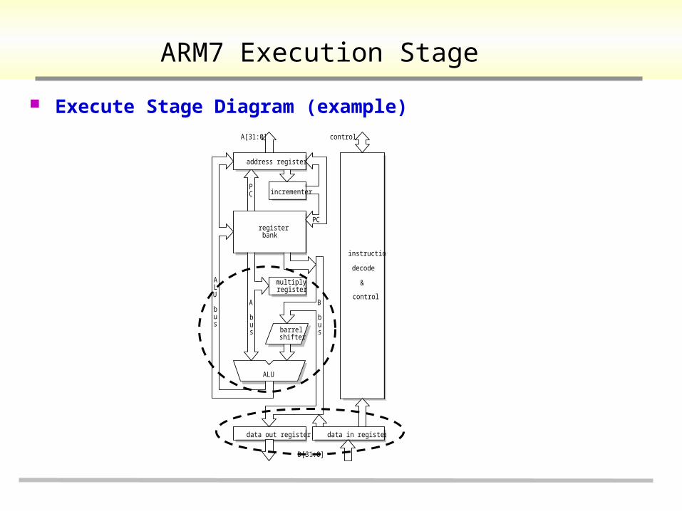
ARM7 Execution Stage
Execute Stage Diagram (example)
multiply
data out register
instruction
decode
&
control
incrementer
registerbank
address register
barrelshifter
A[31:0]
D[31:0]
data in register
ALU
control
PC
PC
ALU bus
A bus
B bus
register
Recommended