© M. Shabany, ASIC/FPGA Chip Design
ASIC/FPGA Chip Design
Mahdi Shabany
Department of Electrical Engineering
Sharif University of technology
Verification

© M. Shabany, ASIC/FPGA Chip Design
Verification
Exponential increase in the complexity of ASIC implies need for sophisticated verification methods to be incorporated in the ASIC design process. Catch the bug as early as possible
So catch it in simulation saves time and money. Imagine respin of a chip if the same bug is caught in Silicon
Verification:
A process that ensures conformance of a design to predefined expectations

© M. Shabany, ASIC/FPGA Chip Design
Verification
Types of Verification:
Functional: Functional verification of RTL
Gate-level simulation:
To verify that the synthesized netlist matches the expected functionality
Formal Verification (equivalence checking): To make sure that the gate level netlist is equivalent to the RTL
Timing Verification:
To verify that the design can run at speed

© M. Shabany, ASIC/FPGA Chip Design
Functional Verification
Two general methods:
Graphical and manually: Inserting inputs and clock manually and run graphical simulations using CAD tools such as Quartus or ISE
o Good for simple designs o Suitable for early evaluations
Automated: Writing testbench to run the simulation/verification automatically
o Suitable for large designs o Suitable for stress testing
© M. Shabany, ASIC/FPGA Chip Design
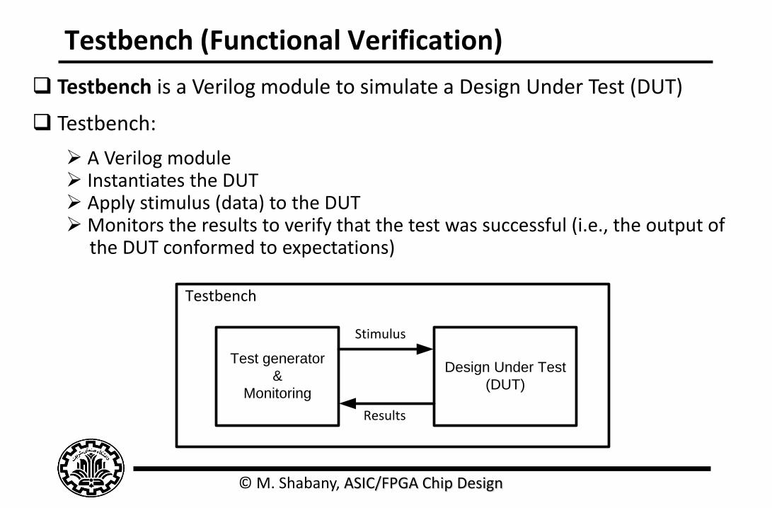
Testbench (Functional Verification)
Testbench is a Verilog module to simulate a Design Under Test (DUT)
Testbench:
A Verilog module Instantiates the DUT Apply stimulus (data) to the DUT Monitors the results to verify that the test was successful (i.e., the output of the DUT conformed to expectations)
Test generator
&
Monitoring
Design Under Test
(DUT)
Testbench
Stimulus
Results

© M. Shabany, ASIC/FPGA Chip Design
Testbench

© M. Shabany, ASIC/FPGA Chip Design
Testbench (Functional Verification)
Simulation of Verilog designs takes the following steps:
Compilation & Elaboration:
The simulator reads the design description, processes compiler directives, and builds a data structure that defines the design hierarchy.
Initialization: The simulator initializes module parameters, storage elements and nets. When simulation starts at time zero, the simulator propagates these changes and executes the statements in each initial and always block up to a timing control.
Simulation:
The simulator processes events and applies them to the DUT The results are displayed and/or saved for investigation

© M. Shabany, ASIC/FPGA Chip Design
Verilog Simulation Commands:
The Verilog includes compiler directives and system tasks to control the simulation of a Verilog mode
`<directive> compiler directives:
Executed prior to simulation time zero Instructions to simulators on how to compile models Always start with a ` accent grave (the “back tic”)
$<task> system tasks:
Executed during simulation (i.e.: to display values) Used as programming statements Always start with a $ dollar sign
`include `timescale `define
$monitor $display $time
© M. Shabany, ASIC/FPGA Chip Design
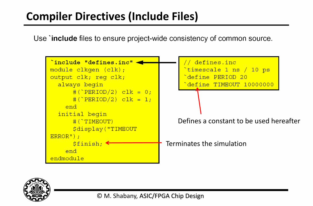
Compiler Directives (Include Files)
Defines a constant to be used hereafter
Terminates the simulation

© M. Shabany, ASIC/FPGA Chip Design
Compiler Directives (Time Scale)
Unit/Precision Delay Specification Time Delayed Comments
1 ns/ 1ns #3 3ns
10 ns/ 1ns #3 30ns Delay is 3*10ns (time unit)
10 ns/ 1ns #3.2 32ns 3.2 is multiplied by 10
10 ns/ 1ns #3.36 34ns
10 ns/ 10ns #3.2 30ns
10 ns/ 100ps #3.748 37.5ns 3.748 is multiplied by 10 and rounded to 2 decimal place
1 ns/ 1ns #3.22 3ns
`timescale is used to define time delay unit/precision :
`timescale 10ns/1ns

© M. Shabany, ASIC/FPGA Chip Design
System Tasks ($display)
$time: Returns the current simulation time as a 64-bit unsigned integer
The returned value is scaled to the time unit of the module that invoked it
$display: Immediately displays the values of its arguments
Example:
$display (“format string”, argument list)
$display (“Reset is = %b and Clock is = %b \n”, Reset, Clk)
Reset is = 1 and Clock is = 0
Reset is = 1 and Clock is = 1
Reset is = 0 and Clock is = 0
Reset is = 0 and Clock is = 1

© M. Shabany, ASIC/FPGA Chip Design
System Tasks ($display)
$display: supports multiple default radixes
$displayb (binary)
$displayd (decimal)
$displayh (hexadecimal)
$displayo (octal)
Formatters and Escaped literals can be used inside the format string.
Formatters can be used to overrides the default radix
Formatters:
Escaped literals:
%b %c %h %d %t %o %s
\” (double quote) \n (new line) \\(backslash) \t(tab)

© M. Shabany, ASIC/FPGA Chip Design
System Tasks ($monitor)
$monitor: to monitor changes in the signal values in its argument list
Continuously monitors the variables in its argument list and displays the formatted
arguments at the end of each simulation time in which any of signals changes value
Only one $monitor system task can be active. Any subsequent invocation of
$monitor starts monitoring the new signal arguments and discontinues monitoring
the previous signal arguments.
$monitoroff and $monitoron system tasks can be used to restrict monitoring to
intervals of time, rather than monitoring entire remainder of simulation session.
The $monitor system task accepts the same formatters/argument list as $display.
$monitor (“format string”, argument list)

© M. Shabany, ASIC/FPGA Chip Design
File Open/Close
The stimulus can be read from a file and then applied to the DUT
A file can be opened for reading or writing, and the syntax is as below:
All fopen options:
A file can be closed as follows:
file = $fopen("filename",r); // For reading
file = $fopen("filename",w); // For writing
file = $fclose("filename”);
“r” or “rb” Open for reading
“w” or “wb” Truncate to zero length or create for writing
“a” or “ab” Append (open for writing at end of file)
“r+”, “r+b”, or “rb+” Open for update (reading and writing)
“a+”, “a+b”, or “ab+” Append; Open or create for update at end-of-file

© M. Shabany, ASIC/FPGA Chip Design
Initial Construct
Initial: Same as always except that whatever that is inside it executes only once
Used for initialization at the beginning of the testbench
Any signal assigned a value inside it should be of type variable (e.g., reg)
module test (); `timescale 1ns/1ns; reg Clk, Reset, in; wire Out; Moore DUT(in, Clk, Reset, Out); initial begin Clk = 1’b0; in = 1’b0; Reset = 1’b1; end initial #10 Reset = 1’b0; always #5 Clk = ~Clk; initial #7 in = 1’b1; endmodule
A clock with 10ns period
Executes only once (as opposed to always)
Top module instantiation
Requires begin-end
for multiple statements Clk
in
Reset
0 5 10 15 20 25 30 35
© M. Shabany, ASIC/FPGA Chip Design
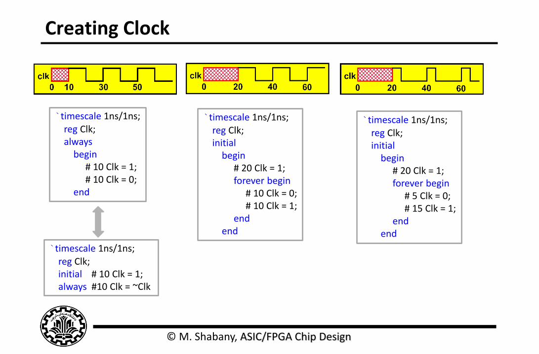
Creating Clock
`timescale 1ns/1ns; reg Clk; always begin # 10 Clk = 1; # 10 Clk = 0; end
`timescale 1ns/1ns; reg Clk; initial begin # 20 Clk = 1; forever begin # 10 Clk = 0; # 10 Clk = 1; end end
`timescale 1ns/1ns; reg Clk; initial begin # 20 Clk = 1; forever begin # 5 Clk = 0; # 15 Clk = 1; end end
`timescale 1ns/1ns; reg Clk; initial # 10 Clk = 1; always #10 Clk = ~Clk

© M. Shabany, ASIC/FPGA Chip Design
Applying Stimulus
Common stimulus application techniques are:
In-line stimulus, applied from an initial block
Stimulus applied from a loop or always block
Stimulus applied from an array of vectors or integers

© M. Shabany, ASIC/FPGA Chip Design
In-Line Stimulus
fork-join construct is used to execute them all in parallel

© M. Shabany, ASIC/FPGA Chip Design
In-Loop Stimulus
In-Loop stimulus

© M. Shabany, ASIC/FPGA Chip Design
Random Stimulus
Initial repeat (13) #5 Clk = ~Clk; Initial repeat (10) #6 In = $random; Initial forever @(posedge Clk) #3 In2 = $random
$random: Returns a 32-bit signed integer random value
There are two ways to terminate simulations
$stop:
A stopped simulation can be resumed after termination
$finish:
A finished simulation can NOT be resumed after termination
“In” receives random data 10 times every 6 time units
Initial #180 $stop; Initial #180 $finish;
Both terminate simulation after 180 time units
3 time units after the posedge Clk, In2 gets a new data
(No overlapping b/w data and Clk)

© M. Shabany, ASIC/FPGA Chip Design
Task Construct in Testbench
Clock period: 20 time units

© M. Shabany, ASIC/FPGA Chip Design
Applying Stimulus
Make sure you understand the timing transitions:
reg [10:0] Count; reg [3:0] A; always @ (posedge Clk) begin if ( !Rst ) A <= 4’b0; else if ( Count == 3) A <= 4’b2; end always @ (posedge Clk) begin if ( !Rst ) Count <= 11’b0; else Count <= Count + 1; end
Clk
Rst
Count 0 1 2 3 4 5
A 0 20 0 0 2

© M. Shabany, ASIC/FPGA Chip Design
Applying Stimulus
If another block wants to sample “SUM” value, it has to sample it when or after Count is 4.
reg [3:0] a, b; wire [3:0] SUM; always @ (posedge Clk) begin if ( Count == 1 ) a <= 4’b0101; else if ( Count == 3) b <= 4’b1010; end assign SUM = a+b;
Clk
Count 0 1 2 3 4 5
a 0101 0101 0101 0101
b 1010 1010
SUM 1111 1111

© M. Shabany, ASIC/FPGA Chip Design
Applying Stimulus
Example:
module Counter(clk, reset, out); input clk, reset; output [2:0] out; reg [2:0] count; always @ (posedge clk) begin if (reset) count <= 0; else if (count == 3'b111) count <= 3'b000; else count <= count +3'b1; end assign out = count; endmodule
`timescale 1 ps/ 1 ps module Counter_tb(); reg clk, reset; wire [2:0] out; Counter i1 (.clk(clk),.out(out),.reset(reset)); initial
clk=0; always begin
#5 clk = 1; #5 clk = 0; $monitor("Reset is = %b and Clock is = %b \n", Reset, Clk);
end endmodule
Module Testbench
© M. Shabany, ASIC/FPGA Chip Design
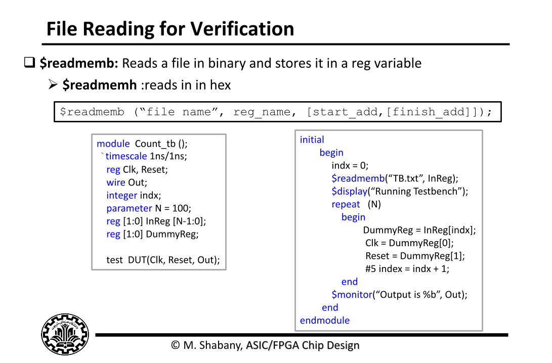
File Reading for Verification
$readmemb: Reads a file in binary and stores it in a reg variable
$readmemh :reads in in hex
$readmemb (“file name”, reg_name, [start_add,[finish_add]]);
module Count_tb (); `timescale 1ns/1ns; reg Clk, Reset; wire Out; integer indx; parameter N = 100; reg [1:0] InReg [N-1:0]; reg [1:0] DummyReg; test DUT(Clk, Reset, Out);
initial begin indx = 0; $readmemb(“TB.txt”, InReg); $display(“Running Testbench”); repeat (N) begin DummyReg = InReg[indx]; Clk = DummyReg[0]; Reset = DummyReg[1]; #5 index = indx + 1; end $monitor(“Output is %b”, Out); end endmodule
© M. Shabany, ASIC/FPGA Chip Design
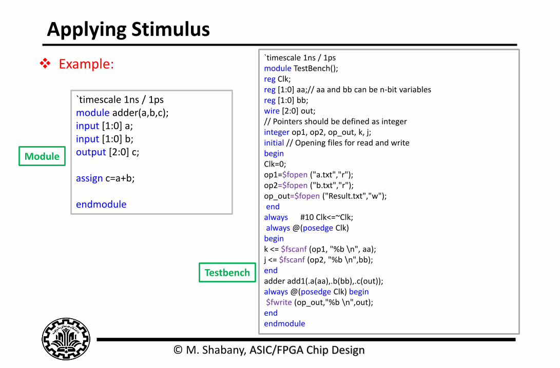
Applying Stimulus
Example:
`timescale 1ns / 1ps module adder(a,b,c); input [1:0] a; input [1:0] b; output [2:0] c; assign c=a+b; endmodule
Module
Testbench
`timescale 1ns / 1ps module TestBench(); reg Clk; reg [1:0] aa;// aa and bb can be n-bit variables reg [1:0] bb; wire [2:0] out; // Pointers should be defined as integer integer op1, op2, op_out, k, j; initial // Opening files for read and write begin Clk=0; op1=$fopen ("a.txt","r"); op2=$fopen ("b.txt","r"); op_out=$fopen ("Result.txt","w"); end always #10 Clk<=~Clk; always @(posedge Clk) begin k <= $fscanf (op1, "%b \n", aa); j <= $fscanf (op2, "%b \n",bb); end adder add1(.a(aa),.b(bb),.c(out)); always @(posedge Clk) begin $fwrite (op_out,"%b \n",out); end endmodule
© M. Shabany, ASIC/FPGA Chip Design
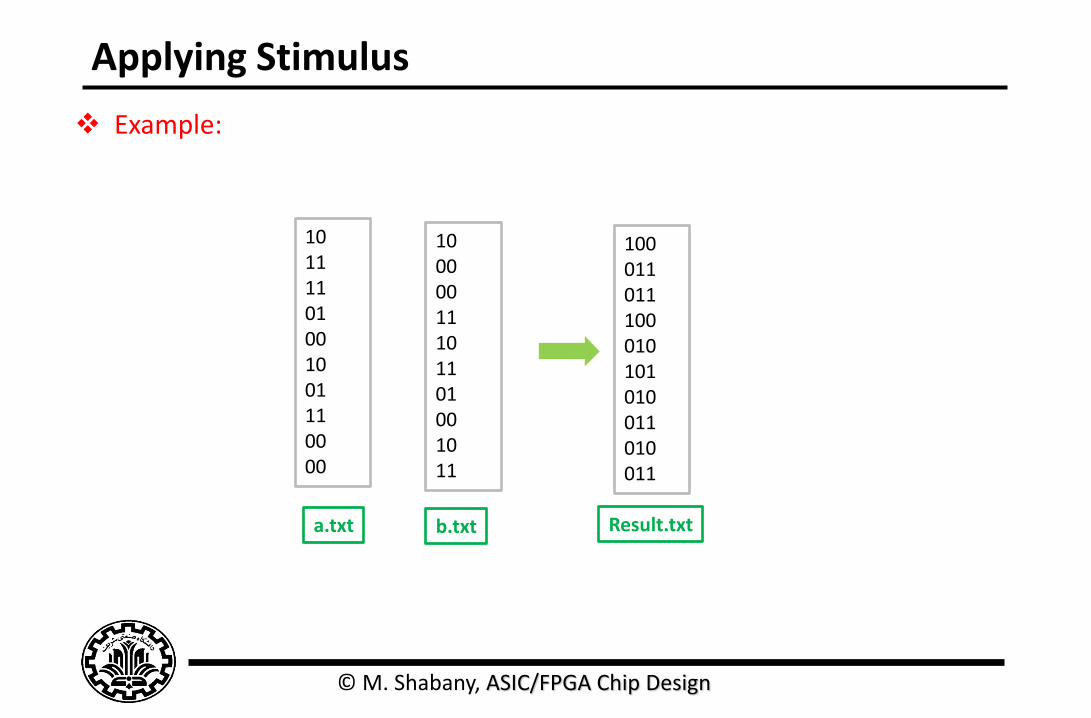
Applying Stimulus
Example:
10 00 00 11 10 11 01 00 10 11
a.txt Result.txt
10 11 11 01 00 10 01 11 00 00
100 011 011 100 010 101 010 011 010 011
b.txt
© M. Shabany, ASIC/FPGA Chip Design
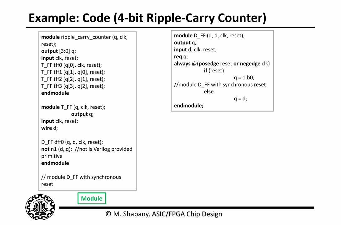
Example: Code (4-bit Ripple-Carry Counter)
module ripple_carry_counter (q, clk, reset); output [3:0] q; input clk, reset; T_FF tff0 (q[0], clk, reset); T_FF tff1 (q[1], q[0], reset); T_FF tff2 (q[2], q[1], reset); T_FF tff3 (q[3], q[2], reset); endmodule module T_FF (q, clk, reset); output q; input clk, reset; wire d; D_FF dff0 (q, d, clk, reset); not n1 (d, q); //not is Verilog provided primitive endmodule // module D_FF with synchronous reset
Module
module D_FF (q, d, clk, reset); output q; input d, clk, reset; req q; always @(posedge reset or negedge clk) if (reset) q = 1,b0; //module D_FF with synchronous reset else q = d; endmodule;

© M. Shabany, ASIC/FPGA Chip Design
Example: Testbench
module stimulus; req clk; req reset; wire [3:0] q; //instantiate the design block; Ripple_carry_counter r1(q, clk, reset); //control the clk signal that drives the design block //cycle time = 10 initial clk = 1’b0; //set clk to 0 always #5 clk = ~clk; //toggle clk every 5 time units //control the clk signal that drives the design block //reset the arrested from 0 to 20 and from 200 to 220. initial begin reset = 1’b1; #15 reset = 1’b0; #180 reset = 1’b1; #10 reset = 1’b0; #20 $finish; //terminate the simulation end
Testbench
//monitor the outputs initial Smonitor($time, “output q = %d”, q); endmodule

© M. Shabany, ASIC/FPGA Chip Design
Example : Results
0 output q = 0
20 output q = 1
30 output q = 2
40 output q = 3
50 output q = 4
60 output q = 5
70 output q = 6
80 output q = 7
90 output q = 8
100 output q = 9
110 output q = 10
120 output q = 11
130 output q = 12
140 output q = 13
150 output q = 14
160 output q = 15
170 output q = 0
180 output q = 1
190 output q = 2
195 output q = 0
210 output q = 1
220 output q = 2
Result
© M. Shabany, ASIC/FPGA Chip Design
Simulation Tool: Modelsim
We use Modelsim as the simulation tool for our testbenches
Modelsim can also compile the design
The tutorial for Modelsim should be read and done with the files provided on the course website.
Recommended