ATOMISTIC MODELING OF THE MICROSTRUCTURE AND TRANSPORT
PROPERTIES OF LEAD-FREE SOLDER ALLOYS
by
Michael S. Sellers
August 23, 2010
A dissertation submitted to the Faculty of the Graduate School of the
University at Buffalo, State University of New York in partial fulfillment
of the requirements for the degree of
Doctor of Philosophy
Department of Chemical and Biological Engineering
Advisors: David A. Kofke and Cemal Basaran

ii
Copyright by
Michael S. Sellers
2010
Copyright

iii
I would like to recognize the following people for their help, in one way or another,
towards the completion of this work.
My advisors, Dr. Cemal Basaran and Dr. David A. Kofke. I am very fortunate to have
worked for such skilled and understanding people. They spared no effort in providing me
countless hours of guidance and chances to grow professionally. I owe each of them a
great deal.
My committee member and mentor, Dr. Jeffrey R. Errington. Jeff has been a source of
help and encouragement since the start of my research career and I am grateful for all the
opportunities he has afforded me.
Acknowledgments

iv
My research professor and friend, Dr. Andrew J. Schultz. NOBODY deserves such a
selfless mentor! His chief quality is his unwavering patience...patience, and
knowledge...knowledge and patience...His two principal qualities are his considerable
knowledge and unwavering patience...and his willingness to help...His three top qualities
are his considerable knowledge, unwavering patience, and willingness to help...and his
valuable and sincere opinions. His four...no...Amongst his qualities...Composing
Andrew’s character are such elements as unwavering patience, considerable knowledge...
I’ll tell him in person.
My group members and friends. Particularly Tai Boon Tan, Katherine Shaul, Hye Min
Kim, and Nancy Cribbin. I could not ask for better lab mates. I envy their talent and
motivation, and will enjoy watching their continued success in the coming years. Our
humorous discussions, group parties, and relaxing lunches will be missed. Also, Shidong
Li, Bicheng Chen, Tarek Regab, Yongchang Lee, and Eray Gunel of the Electronics
Packaging Laboratory, and Peter Mersich, Thomas Rosch, Eric Grzelak, and Ravi
Chopra. Graduate school was enjoyable because of such wonderful friends.
My parents, my sister, and Diane Youker. I could not have done this without them. My
conversations with Diane make the tough days much easier and her love and
companionship gives me something wonderful to come home to. I also thank my sister
Liz for all her encouragement. And finally, I am truly grateful for my parents’ support
and love. I owe a part of everything I accomplish to you both.

v
Copyright ........................................................................................................ ii
Acknowledgments ......................................................................................... iii
Table of Contents ............................................................................................. v
Tables and Figures .......................................................................................... ix
Abstract .......................................................................................................... xv
Published Work ......................................................................................... xviii
Introduction ...................................................................................................... 1
1.1 Modeling Damage Mechanics in Solder Joints .................................................. 2
1.1.1 Electromigration and Other Damage Phenomena ........................................... 4
1.1.2 Thermodynamic Models and the Atomistic Realm ........................................ 7
1.2 Objectives ......................................................................................................... 10
Table of Contents

vi
1.3 Outline............................................................................................................... 10
Models and Methodology for Surfaces and Interfaces .................................. 12
2.1 Material Structures and Molecular Models ....................................................... 13
2.1.1 Modeling �Sn, and Sn-Ag, Sn-Cu Alloys .................................................... 13
2.1.2 Crystal Lattice Structures .............................................................................. 19
2.1.3 Constructing Interfaces ................................................................................. 20
2.2 Computing Transport Properties ....................................................................... 22
2.2.1 Mechanism Search with the Dimer Method ................................................. 22
2.2.2 Diffusivity from Harmonic Transition State Theory .................................... 26
2.2.3 Diffusivity Computation Techniques with Molecular Dynamics ................. 27
2.3 Energetics and Structure of Surfaces and Interfaces ......................................... 31
2.3.1 Excess Potential Energies of Surfaces and Interfaces ................................... 31
2.3.2 Solute Contributions to Interfacial Energy ................................................... 34
2.3.3 Identifying Regions of Structure in Grain Boundaries ................................. 36
2.4 Atomic Level Stress: An Introduction and Case Study .................................... 37
2.4.1 Macroscale Connection to Atomic Stress ..................................................... 37
2.4.2 Relationships for Volumetric Strain ............................................................ 38
2.4.3 Embedded-Atom Method.............................................................................. 40
2.4.4 Virial Stress ................................................................................................... 42
2.4.5 Molecular Dynamics Simulation of Lattice Vacancy ................................... 43
2.4.6 Computing the Volumetric Strain from Simulation ...................................... 44
2.4.7 Validation with Continuum Mechanics Methods ......................................... 46
2.4.8 Conclusions ................................................................................................... 48
Surface Energies and Adatom Diffusivity ..................................................... 50
3.1 Simulation Details ............................................................................................. 52
3.2 Results and Discussion ..................................................................................... 55
3.2.1 Surface Energy Calculation for �Sn ............................................................. 55

vii
3.2.2 Surface Diffusion on (100) ........................................................................... 56
3.3 Conclusions ....................................................................................................... 60
Grain Boundary Structure and Self-Diffusivity ............................................ 62
4.1 Simulation Details ............................................................................................. 64
4.2 Results and Discussion ..................................................................................... 65
4.2.1 Grain Boundary Excess Potential Energies .................................................. 65
4.2.2 Grain Boundary Width-Scaled Diffusivity (�GBDGB) ................................... 66
4.2.3 Grain Boundary Width Calculation .............................................................. 68
4.2.4 Resolving the Grain Boundary Diffusivity (DGB) ......................................... 75
4.2.5 Analysis of In-plane Directional Diffusivity ................................................ 77
4.3 Conclusions ....................................................................................................... 80
Solute Effects on Grain Boundary Energy and Shear Stress......................... 83
5.1 Simulation Details ............................................................................................. 85
5.2 Results and Discussion ..................................................................................... 89
5.2.1 Excess Enthalpy Calculations ....................................................................... 89
5.2.2 Segregation Enthalpies from Molecular Simulation ..................................... 92
5.2.3 Segregation Enthalpies from Experimental Diffusion Measurements .......... 93
5.2.4 Discussion of Experimental Behavior .......................................................... 94
5.2.5 Special Boundary Simulations ...................................................................... 96
5.2.6 Boundary Under Shear Strain ....................................................................... 98
5.2.7 Boundary Sliding in Solute Segregated Boundaries ................................... 104
5.2.8 Interface Structure During High Temperature Sliding ............................... 105
5.3 Conclusions ..................................................................................................... 107
Solute Effects on Grain Boundary Self-Diffusivity .................................... 110
6.1 Simulation Details ........................................................................................... 111
6.2 Results and Discussion ................................................................................... 113
6.2.1 Width-scaled Self-Diffusivity (�GBDGB ) of Sn .......................................... 113

viii
6.2.2 Planar Self-Diffusivity Profiles and Interface Width.................................. 115
6.2.3 Effect of Atomic Size and Cohesive Energy .............................................. 121
6.2.4 Grain Boundary Self-Diffusivity (DGB) of Sn ............................................ 124
6.3 Conclusions ..................................................................................................... 126
Conclusions and Future Work ..................................................................... 129
7.1 Original Contributions .................................................................................... 133
7.2 Recommendations of Future Work ................................................................. 134
References .................................................................................................... 136

ix
List of Tables
Table 2-1 Parameters for the MEAM potential. .............................................................. 18
Table 2-2 Al material properties used in simulations, after Sarychev. [15] .................... 43
Table 2-3 Vacancy relaxation factors as reported by authors. ......................................... 45
Table 3-1 Dimer method parameters. .............................................................................. 54
Table 3-2 Surface energies �s of �Sn, Cu, Ag, and Al with respect to Miller plane orientation. Cu, Ag, and Al are reproduced from [19]. ................................................ 55
Table 3-3 Mechanism data. Respectively, the adatom direction, mechanism activation energy, attempt frequency, distance the adatom traveled, and tracer diffusivity at 300K are specified. .................................................................................................................. 58
Table 4-1 Excess Interfacial Potential Energies (mJ/m2) at 300K. .................................. 66
Table 4-2 Arrhenius properties calculated from experiment in ref [10]. ......................... 67
Tables and Figures
x
Table 4-3 Arrhenius Properties of Simulated Grain Boundaries from weighted least squares fit, 325K to 450K .............................................................................................. 76
Table 5-1 Ag and Cu solute quantities and corresponding excess interfacial density. .... 86
Table 5-2 Ag solute calculations of enthalpy of segregation (�Hseg), critical excess interfacial concentration (�cr), and critical number of solute atoms (NA,cr). Error is a weighted least squares fit on Figure 5-3– Ag slope. ..................................................... 91
Table 5-3 Cu solute calculations of enthalpy of segregation (�Hseg), critical excess interfacial concentration (�cr), and critical number of solute atoms (NA,cr). Error is a weighted least squares fit on Figure 5-3– Cu slope. ...................................................... 91
Table 5-4 Ag and Cu solute calculations of enthalpy of segregation (�Hseg) for various boundaries of �Sn at 300K. Error is a weighted least squares fit of HEX,GB+S vs.��EX. . 97
Table 6-1 Ag and Cu solute quantities and corresponding excess interfacial density. .. 112
List of Figures
Figure 1-1 Damage from high electrical current density in PbSn solder joint. Red arrows indicate direction of electron flow. .................................................................................. 3
Figure 1-2 A multi solder joint finite element model. Arrows indicate direction of electrical current flow. [4] ................................................................................................ 4
Figure 1-3 Electron wind effect on metal atoms, the main driving force in electromigration. .............................................................................................................. 5
Figure 1-4 An SEM image of a solder joint microstructure colored by �Sn grain orientation. ..................................................................................................................... 10
Figure 2-1 Crystal structures of �Sn (TOP) and its alloys in L12 (BOTTOM) represented by the MEAM potential. Dimensions on lattice indicate tetragonal crystal structure (TOP) and cubic crystal structure (BOTTOM). Lattice images courtesy of ref. [29]. . 19
Figure 2-2 Shown LEFT are various Miller planes in �Sn's lattice. RIGHT is the rotation of two grains to share a common Miller plane. Red, Blue, and Purple, are (101), (201), and (401) Miller planes, respectively. Green and Orange are (310) and (410), respectively. Note that the side view x-direction is stretched for figure height conformity. X-direction corresponds to the lattice a-direction, [100]; Z-direction corresponds to the lattice c-direction, [001]. ................................................................. 20

xi
Figure 2-3 Simulation snapshot of the (101) grain boundary of �Sn. Dark atoms are Sn, green are Ag solute at the interface. Structure is 3-dimensional and view is looking down the y-direction at the x-z plane. ............................................................................ 21
Figure 2-4 (1) Typical locations on the energy hyper-surface for minima and saddle points. (2) An atomistic system represented by a point on the energy hyper-surface. (3) Multiple points (systems) with their distance in hyper-surface space maintained. Colored hyper surface adapted from ref [33]. ................................................................ 24
Figure 2-5 When tracing the path of minimum energy from the saddle point to minimum, the dimer is rotated to a minimum energy via steepest descent (a) and then stepped (b), maintaining the correct orientation along the lowest curvature mode. This routine is repeated until the center of the dimer is at a minimum energy. ..................................... 25
Figure 2-6 Planar diffusivity vs. z-coordinate in the simulation cell. [h] is the maximum if the diffusion profile and [�] is the width at [h]/2. Background is grain boundary rotated with z-axis parallel to planar diffusivity plot abscissa. Points on plot correspond to lattice planes in background separated by �z. ........................................................... 30
Figure 2-7 The two systems considered in excess potential energy calculations of a free surface. Orange lines are Miller planes; Green dashed lines are fixed free surfaces. ... 32
Figure 2-8 The three systems considered in excess potential energy calculations of a grain boundary. Orange lines are Miller planes; Green dashed lines are fixed free surfaces. ......................................................................................................................... 33
Figure 2-9 The variation of |S(k)|2, for a bulk solid at 0K and 300K, and a grain boundary at 300K. Note the abscissa is the direction perpendicular to the interface. Error bars represent the standard deviation of |S(k)|2 in five snapshots of an MD run. 37
Figure 2-10 A plot of first-nearest neighbor distance from center of an atom (or void), versus simulation time steps in molecular dynamic simulations. Filled black circles indicated a full lattice and open circles indicate a vacancy, where the atom is removed at 10ps into the data collection run. Average neighbor positions before and after atom removal are 2.891 +/-0.009 and 2.831 +/-0.010, respectively. ...................................... 45
Figure 2-11 Void model in continuum mechanics domain. ............................................. 47
Figure 2-12 Free body diagram under spherical coordinate system. ............................... 47
Figure 3-1 LEFT a z-direction, top view of the (100) surface. RIGHT a 3-dimensional view of the simulation cell. Atoms are colored white to denote movable by the dimer method and gray for fixed. ............................................................................................. 54

xii
Figure 3-2 Energy maps of the �Sn (100) surface. Left. Red denotes a higher energy (ion cores), blue denotes lower energy. Right. Diamonds are respective saddle point locations of the adatom, white circles are minima locations. ........................................ 57
Figure 3-3 Energy values along the minimum energy path for the given mechanisms. Values along the reaction coordinate are corrected to a baseline value of the minimum energy configuration—both mechanisms begin and finish at 0eV. Diamonds denote energies corresponding to saddle point configurations. ................................................. 58
Figure 3-4 Arrhenius plot of diffusivity with respect to inverse temperature. ................ 60
Figure 4-1 (1) Minimization (near 0K-MD), (2) Equilibration, and (3) Production structures. Actual simulation cells are 3-dimensional and periodic in x and y-directions. ....................................................................................................................... 65
Figure 4-2 Arrhenius plot of scaled diffusivity vs. temperature. Points are results for various symmetric tilt grain boundaries simulated in this work. Dark lines are experimental data from Singh and Ohring. [9] Error bars represent standard deviation of three independent simulations and computations of �GBDGB . ................................... 67
Figure 4-3 Planar diffusivity for various grain boundaries at 300K (left) and 450K (right). Note the different scales for each temperature, but similar scales for z. Lines are guides for the eye. .................................................................................................... 69
Figure 4-4 Square planar structure factor vs. z-axis plane for the five grain boundaries studied. Colors are different temperatures. Blue-300K, Green-350K, Orange-400K, Red-450K. Error bars represent the standard deviation of |S(k)|2 in five snapshots from an MD run. ..................................................................................................................... 71
Figure 4-5 TOP and BOTTOM are snapshots of the (101) GB at 300K and 450K, respectively. LEFT is looking parallel to the grain tilt axis and at RIGHT looking perpendicular. ................................................................................................................. 72
Figure 4-6 Diffusive (open points, left) and structural widths (filled points, right) versus temperature for the five grain boundaries studied. Lines are guides for the eye. Black lines is the diffusive width used in ref [9]. ..................................................................... 73
Figure 4-7 An Arrhenius plot of grain boundary diffusivity vs. temperature. Shown as colored points are various symmetric tilt grain boundaries simulated in this work. Dark lines are experimental data from Singh and Ohring. Error bars represent standard deviation of three or more independent simulations. ..................................................... 77
Figure 4-8 Arrhenius plots of scaled directional diffusivity vs. temperature. Left are (310) and (410) grain boundaries, Right are (101), (201), and (401) grain boundaries.
xiii
Filled points are diffusion in a direction perpendicular to the grain tilt axis; Open points are diffusion in a direction parallel to the grain tilt axis. Letters in parentheses in the plot legends are crystal lattice directions of diffusion. Error bars represent standard deviation of three or more independent simulations. ..................................................... 79
Figure 4-9 Simulation snapshot of (401) grain boundary at 450K. LEFT is looking down the grain tilt axis and at RIGHT the grain tilt axis is oriented left/right. ....................... 80
Figure 5-1 Typical configuration of grain boundary with its interface loaded with solute (orange). LEFT is a simulation snapshot after equilibration and RIGHT is the same snapshot with the interface exposed for clarity. ............................................................. 86
Figure 5-2 (1) Grain boundary minimization (near 0K), (2) Solute minimization, (3) NPT MD equilibration, (4) NVT MD Shear simulation. Filled arrows indicate direction of motion of the block portion. Orange circles are solute at interface. Free atoms are movable in x, y, and z directions. Actual simulation cells are 3-dimensional and periodic in x and y directions. ........................................................................................ 87
Figure 5-3 Difference in the excess enthalpies of the solute loaded grain boundary and bulk �Sn with an equal amount of solute (HEX,GB+S) vs. excess solute concentration (�EX). Error is the standard deviation. Trend lines are fitted by a weighted least-squares analysis. ............................................................................................................. 90
Figure 5-4 Shear stress (�xz) vs. average strain (�avg) for four strain rates at 300K. Curve labels point to yield stress in various shear strain rates, decreasing from top to bottom. Lowest label is stoppage of shear rate of 6.25x10⁶ s-1 at a strain of 0.0375, to simulate a steady state condition. .................................................................................................... 99
Figure 5-5 Shear stress (�xz) vs. average strain (�avg) for three solute amounts of Ag at 300K and 450K. Number in squares are solute atom amounts. Curves at 300K are the average of three independent simulation runs. Note different scales for 300K and 450K. ............................................................................................................................ 101
Figure 5-6 Shear stress (�xz) vs. average strain (�avg) for three solute amounts of Cu at 300K and 450K. Number in squares are solute atom amounts. Curves at 300K are the average of three independent simulation runs. Note different scales for 300K and 450K. ............................................................................................................................ 102
Figure 5-7 Structural formation in pure GB interface at 450K under shear. (1) Side view in y-z plane. (2) Side view in x-z plane, shear direction indicated. (3) Top view of full BCC structure and separate lattice planes. ................................................................... 107
xiv
Figure 6-1 (1) minimization (MD near 0K), (2) solute minimization (conjugate gradient), (3) equilibration, (4) production structures. Black arrows indicate direction of motion of the block portion. Free atoms are movable in x, y, and z directions. Actual simulation cells are 3-dimensional and periodic in x and y directions. ....................... 112
Figure 6-2 Width-scaled self-diffusivity of Sn vs. temperature for various solute atom quantities. LEFT is Ag solute, RIGHT is Cu solute. Error bars are standard deviation from three or more simulation runs. ............................................................................ 115
Figure 6-3 Planar self-diffusivity profiles in z-direction of Sn for various solute atom quantities of Ag at a particular temperature. Note different scales on each ordinate. 117
Figure 6-4 Self-planar diffusivity profiles in z-direction of Sn for various solute atom quantities of Cu at a particular temperature. Note different scales on each ordinate. 118
Figure 6-5 Diffusive width vs. temperature for various solute concentrations. LEFT is Ag and RIGHT is Cu. Circle points (black) are the pure �Sn grain boundary widths....................................................................................................................................... 119
Figure 6-6 Rendered simulation snapshot of two grain boundaries at 450K and containing 50 solute atoms in the interface. LEFT is Ag (green) and RIGHT is Cu (orange). ....................................................................................................................... 121
Figure 6-7 Self-planar diffusivity profiles of �Sn in z-direction for solute atom quantities of 50 at various temperatures. LEFT is Ag and RIGHT is Cu. Note different scales on ordinate. ....................................................................................................................... 124
Figure 6-8 Self-diffusivity of Sn vs. temperature for various solute atom quantities. LEFT is Ag solute, RIGHT is Cu solute. ..................................................................... 126

xv
Damage mechanics models of lead-free solder joints in nanoelectronics continue to
improve, and in doing so begin to utilize quantitative values describing processes at the
atomic level, governing phenomena like electromigration and thermomigration. In
particular, knowledge of the transport properties of specific microstructures helps
continuum level models fully describe these larger-scale damage phenomena via multi-
scale analysis. For example, diffusivities for different types of grain boundaries (fast
diffusion paths for solvent and solute atoms, and vacancies), and a description of the
boundary structure as a function of temperature, are critical in modeling solder
microstructure evolution and, consequently, joint behavior under extreme temperature
and electric current. Moreover, for damage that develops at larger length scales, surface
Abstract
xvi
energies and diffusivities play important roles in characterizing void stability and
morphology.
Unfortunately, experiments that investigate these kind of damage phenomena in the
atomistic realm are often inconsistent or unable to directly quantify important parameters.
One case is the particular transport and structural properties of grain boundaries in Sn
(the main component in lead-free solder alloys) and their behavior in the presence of Ag
and Cu impurities. This information is crucial in determining accurate diffusivity values
for the common SnAgCu (SAC) type solder. Although an average grain boundary
diffusivity has been reported for polycrystalline Sn in several works, the value for grain
boundary width is estimated and specific diffusivities for boundaries known to occur in
Sn have not been reported, to say nothing of solute effects on Sn diffusivity and grain
boundary structure. Similarly, transport properties of Sn surfaces remain relatively
uninvestigated as well. These gaps and inconsistencies in atomistic data must be
remedied for micro- and macro-scale modeling to improve.
As a complement to experimental work and possessing the ability to fill in the gaps,
molecular simulation serves to reinforce experimental predictions and provide insight
into the atomistic processes that govern studied phenomena. In the present body of work,
we employ molecular statics and dynamics simulations in the characterization and
computation of �Sn surface energies and surface diffusivities, the determination of
diffusivities and structural properties of specific �Sn grain boundaries, and the
investigation of Cu and Ag solute effects on �Sn grain boundaries.

xvii
In our study of �Sn surfaces, energies for low number Miller index surfaces are
computed and the (100) plane is found to have the lowest un-relaxed energy. We then
find that two simple hopping mechanisms dominate adatom diffusion transitions on this
surface. For each, we determine hopping rates of the adatom and compute its tracer
diffusivity.
Our work on grain boundaries investigates the self-diffusion properties and structure of
several �Sn symmetric tilt grain boundaries using molecular dynamics simulations. We
find that larger diffusive widths are exhibited by higher excess potential energy grain
boundaries. Diffusivities in the directions parallel to the interface plane are also
computed and activation energies are found with the Arrhenius relation. These are shown
to agree well with experimental data.
Finally, we examine the effect that solute atoms of Ag and Cu have on the
microstructure of �Sn. Excess energies of the (101) symmetric tilt �Sn grain boundary
are computed as a function of solute concentration at the interface, and we show that Ag
lowers the energy at a greater rate than Cu. We also quantify segregation enthalpies and
critical solute concentrations (where the excess energy of the boundary is reduced to
zero). The effect of solute type on shear stress is also examined, and we show that solute
has a strong effect on the stabilization of higher energy grain boundaries under shear
stress. We then look at the self-diffusivity of Sn in the (101) symmetric tilt �Sn grain
boundary and show that adding both Ag or Cu decrease the grain boundary self-
diffusivity of Sn as solute amount in the interface increases. Effects of larger
concentrations of Cu in particular are also investigated.

xviii
Section 2.4 Models and Methods for Surfaces and Interfaces Li, S., Sellers, M.S., Basaran, C., Schultz, A.J., Kofke, D.A. Lattice Strain Due to an Atomic Vacancy. Int. J. Mol. Sci., 10(6), pp 2798-2808 (2009).
Chapter 3 Surface Energies and Adatom Diffusivity Sellers, M.S., Schultz, A.J., Kofke, D.A., Basaran, C. Atomistic Modeling of Tin Surface Energies and Adatom Diffusivity. Applied Surface Science, 256(13), pp 4402-4407 (2010).
Chapter 4 Grain Boundary Structure and Self-Diffusivity Sellers, M.S., Schultz, A.J., Basaran, C., Kofke, D.A. �Sn Grain Boundary Structure and Self-Diffusivity via Molecular Dynamics. Physical Review B, 81(13), pp 4111-4121 (2010).
Chapter 5 Solute Effects on Grain Boundary Energy and Stress Sellers, M.S., Schultz, A.J., Basaran, C., Kofke, D.A. Solute Effects on �Sn Grain Boundary Energy and Shear Stress. Journal of Nanomechanics and Micromechanics. Submitted (August 2010).
Chapter 6 Solute Effects on Grain Boundary Self-Diffusivity Sellers, M.S., Schultz, A.J., Basaran, C., Kofke, D.A. Effect of Cu and Ag Solute Segregation on �Sn Grain Boundary Diffusivity. Physical Review B. Under Review (August 2010).
Published Work

1
As analysis tools in computational materials science develop, transport properties at the
atomistic level play an increasingly important role in the study of a material's behavior at
large scales. Investigations once focused on the study of metals at a macroscopic level,
such as finite element methods (FEM) for example, are now able to reach down into the
nano-scale realm via multi-processor calculations utilizing simulation packages or
software that can connect FEM and molecular simulation. As a result, in the world of
macro-scale simulation, the value of information obtained about a material using
molecular-level simulation techniques is being realized. Quantitative transport data
explaining diffusion, cracking, or crystal growth rates, often difficult to study
experimentally, can be had with relative ease using a molecular simulation package and a
Introduction
“Therefore, since brevity is the soul of wit...”

2
few workstation grade computers. When used in conjunction with a larger-scale model,
this information plays a key part in the description of microstructure and transport
properties, and the phenomena they control at larger length and timescales.
1.1 Modeling Damage Mechanics in Solder Joints
The solder joint presents an interesting system for the application of both continuum and
molecular level simulations. As the metal “glue” connecting almost all electrical
components, from simple capacitors to powerful microprocessors, solder joints face
damage from large temperature and electric current gradients that develop across the
joint, even under normal operation. The effects from temperature and current manifest
themselves as increased mass transport with solid phase growth, vacancy nucleation and
cracking, extrusion at the component or circuit board interfaces, and surface whisker
growth—all leading to the eventual failure or shorting of the joint (figure 1-1). This is
acceptable in most of today’s consumer applications, as the physical lifetime of hardware
is often eclipsed by the lifetime of the hardware’s computing power. However, in high
power applications, or mission-critical scenarios where components are inaccessible for
repair after deployment, eliminating or minimizing solder joint damage is crucial.
Likewise, as electronic devices shrink, so does the joint’s cross-sectional area, thereby
increasing the damage effects of electrical current—reducing these effects is key for the
realization of nanoelectronics.

3
Figure 1-1 Damage from high electrical current density in PbSn solder joint. Red arrows indicate direction of electron flow.
Quite a bit of research has been done at the continuum level on solder joints under
thermal and electrical load. [1][2][3][4] A majority of this work is composed of finite
element models of single or multiple solder joints that can describe the stress,
temperature, and/or current profiles that develop during use. These simulations typically
run faster than real-time, and are used to estimate mean-time-to-failure values for
different joint types. Recent work in this domain has shown decent agreement with
experimental results for older style solder joints, mostly alloys of Pb and Sn. [3] An
example is shown in figure 1-2. In 2003, however, the European Union passed the
Restriction of Hazardous Substances (RoHS) directive—partnered with the Waste
Electrical and Electronic Equipment (WEEE) directive—that effectively removed the Pb
component (among other compounds) from most future commercial electronic devices,
and implemented a recycling program for older, lead-containing, products. [6] Several
North American companies have followed this directive as well, advertising themselves

4
as RoHS Compliant. Replacements for the Pb component in solder vary from binary
mixtures of Sn and Ag, Bi, Cu, In, Sb, or Zn, to combinations of a few of these, but a
majority of the solder alloys in use today are over 90% Sn, 1.0-4.0% Ag, and contain
trace amounts of Cu. [7] Current and temperature effects in these types of joints are equal
to (if not worse than) PbSn joints, making damage modeling and a fundamental
understanding of transport processes leading to this damage a high priority.
Figure 1-2 A multi solder joint finite element model. Arrows indicate direction of electrical current flow. [4]
1.1.1 Electromigration and Other Damage Phenomena
When electric current flows through a solder joint, the momentum of the electrons is
imparted to the ion cores of the metal atoms. [8] At high current density (commonly
measured in Amps/cm2), this momentum exchange leads to the transport of atoms with
the electrons from cathode to anode side, resulting in high vacancy concentration at the
cathode side and pileup or hillocks at the anode side. An example of this is shown in
figure 1-3, where the yellow electron flow pushes the red atom. Impurity (solute) atoms,
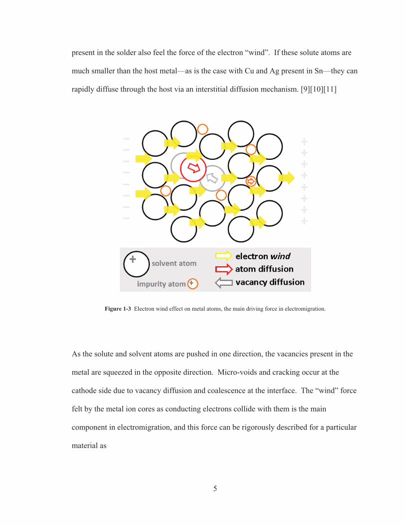
5
present in the solder also feel the force of the electron “wind”. If these solute atoms are
much smaller than the host metal—as is the case with Cu and Ag present in Sn—they can
rapidly diffuse through the host via an interstitial diffusion mechanism. [9][10][11]
Figure 1-3 Electron wind effect on metal atoms, the main driving force in electromigration.
As the solute and solvent atoms are pushed in one direction, the vacancies present in the
metal are squeezed in the opposite direction. Micro-voids and cracking occur at the
cathode side due to vacancy diffusion and coalescence at the interface. The “wind” force
felt by the metal ion cores as conducting electrons collide with them is the main
component in electromigration, and this force can be rigorously described for a particular
material as

6
jeZF
EeZZFFFF
EM
fieldwindEM
fieldwindEM
�*�
���
��
(1-1)
Where FEM is the combination of the electron wind force and the oppositely directed
electric field force. E is the electric field potential, Z* is the effective charge number
(determined by electron wind forces), e is the charge of an electron, � is the resistivity of
the metal, and j is the current density. As the electromigration force induces mass
transfer in the joint, the force of stress counteracts it, where tensile stresses from
vacancies cause cracking and compressive stresses from atom pileup cause extrusion.
The negatively acting force of stress is represented by equation (1-2).
hF �� ��� (1-2)
Here, � is the volume of an atom, and �h is the hydrostatic stress tensor. Additionally,
the force derived from the concentration (or chemical potential) gradient opposes the
electromigration force, and a component of this is the apparent force from a temperature
gradient (dubbed thermomigration) which can aid or counteract the force of
electromigration, depending on the direction of current flow relative to the hot
component and cooler circuit board. Thus, the overall mass diffusion driving force on a
solder joint can now be represented as equation (1-3), where FEM is the electromigration
force, F�� is the thermomigration force, F� is the stress, and F� is the chemical potential
force.

7
�� FFFFF TMEM ���� (1-3)
1.1.2 Thermodynamic Models and the Atomistic Realm
There are a few models that relate the flux or dynamic concentration of vacancies in the
solder joint to the to the various driving forces affecting mass diffusion that are outlined
in equation (1-3). Transport parameters within these models are determined by
experiment, but often through secondary relationships that are not material specific,
providing an avenue by which we can improve these models. In his 1993 work,
Kirchheim explains a relation that connects macro-scale current density and stress
gradients to atomistic vacancy diffusion—describing the change in vacancy flux based on
the vacancy concentration gradient, current density, and stress gradients (respective terms
in equation (1-4) below). [2] Several works apply this relation to aluminum thin films,
and here molecular simulation has been used to determine the volumetric strain
parameter, f, though it is often used inconsistently. [12][13][14] We revisit this point in
Section 2.4. Other parameters such as atomic diffusivity in thin films are still based on
experimental values.
xf
kTcD
eEZkT
cDxc
DJ vvv
vvvvv �
����
��
���*
VJ , vacancy flux vector
VD , effective vacancy diffusivity
eqC , vacancy concentration *Z , vacancy effective charge number
e, electron charge f, vacancy relaxation ratio, the ratio of the volume of an atom and the volume
(1-4)
8
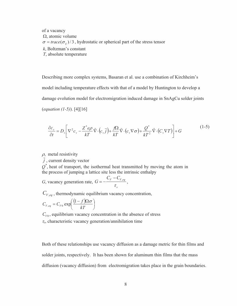
of a vacancy ��, atomic volume
3/)( ijtrace �� � , hydrostatic or spherical part of the stress tensor k, Boltzman’s constant T, absolute temperature
Describing more complex systems, Basaran et al. use a combination of Kirchheim’s
model including temperature effects with that of a model by Huntington to develop a
damage evolution model for electromigration induced damage in SnAgCu solder joints
(equation (1-5)). [4][16]
GTCkTQc
kTfjc
kTeZcD
tc
vvvvvv ��
�
���
�� ��� �
�� ����
�� ����
2
**2 ��
�, metal resistivity j�
, current density vector Q*, heat of transport, the isothermal heat transmitted by moving the atom in the process of jumping a lattice site less the intrinsic enthalpy
G, vacancy generation rate, s
eqVV CCG
�,�
�� ,
eqVC , , thermodynamic equilibrium vacancy concentration,
���
!" ��
�kTfCC VeqV
�1exp0,
0VC , equilibrium vacancy concentration in the absence of stress �s, characteristic vacancy generation/annihilation time
(1-5)
Both of these relationships use vacancy diffusion as a damage metric for thin films and
solder joints, respectively. It has been shown for aluminum thin films that the mass
diffusion (vacancy diffusion) from electromigration takes place in the grain boundaries.

9
This was inferred by observing that the diffusion activation energy determined from
mean-time-to-failure measurements was much lower than bulk aluminum activation
energies, indicating some faster diffusion path other than the pure lattice. [15] Scanning
electron microscope images present a clear picture of the grain boundaries present in pure
Sn and lead-free solder alloys. [17] Figure 1-4 shows the cross-section of a solder joint
microstructure just after solidification. Shades of gray in this image are different
orientations of �Sn grains. The interfaces these grains make with one another are called
grain boundaries and allow for fast atomic diffusion because of low atomic bond
coordination at the interface. Experimental work investigating the type and frequency of
�Sn grain boundaries as a function of temperature, stress, and solute concentration have
reached some important, but very general conclusions about stable boundary types and
the effects of Ag and Cu on Sn microstructure. [17][18] However, specific
characteristics that govern transport within the boundaries, such as a unique diffusivity
and interface thickness, have not be quantified. Similarly, Ag and Cu effects on the
formation of different size grains are not explained in detail, nor is their possible effect on
Sn (vacancy) diffusivity in the boundary. This lack of transport and microstructural
information form the basis for this body of work.

10
Figure 1-4 An SEM image of a solder joint microstructure colored by �Sn grain orientation.
1.2 Objectives
With the opportunities for study developed in the previous section, this dissertation
presents the goal of investigating the various structural regimes of �Sn present in lead-
free solder joints. The transport and microstructure properties of these regimes are
quantified. Additionally, we examine how these various systems react to changes in
temperature and the presence of solute atoms, and provide justified explanations of their
behavior under such conditions.
1.3 Outline
Chapter 2 continues this work, in which the simulation software, structures, and
theoretical relationships used in the subsequent studies of �Sn are explained. Chapter 3
begins our investigation of lead-free solder with the calculation of surface energies and
surface diffusivity, important quantities when modeling large voids that can develop in
joints because of vacancy coalescence and solid phase growth. Next, we quantify the

11
transport characteristics of several grain boundaries of �Sn in Chapter 4 and compare
them to average diffusivity measured from experiment. In Chapter 5, Ag and Cu solute
effects on grain boundary energy leading to stable grain structure are investigated, and
conclusions are drawn to better explain experimental observations of Sn-xAg and Sn-xCu
microstructure formation. We also examine the effects of solute on shear stress as an
additional metric for grain boundary stability. Chapter 6 ends our investigation of the
solder system, by examining to what extent Ag and Cu atoms can aid or hinder Sn
diffusion in the grain boundary. Finally, the general conclusions of the dissertation are
presented and suggestions on future work are offered.

12
As this dissertation continues, the studies of �Sn surfaces and interfaces will draw upon
the simulation techniques, potential models, and relationships defining the properties of
energy, structure, diffusivity, and stress in our simulations, that are outlined here. We
begin with a description of the two primary types of systems studied, a �Sn surface and
various �Sn grain boundaries, and the interatomic potential used. Next, we introduce a
molecular statics technique for investigating diffusion mechanisms, and show how these
results are used for the calculation of specific diffusivities. For systems simulated with
molecular dynamics and exhibiting complex structure, modifications to the standard
Einstein relation are then outlined for use in computing diffusivity in non-bulk like
regions of a solid. Following this, quantities describing the difference in energy and
Models and Methodology for Surfaces and Interfaces
“Though this be madness, yet there is method in't.”

13
structure in comparison to bulk �Sn are developed. We then conclude this section with
an introduction to atomic level stress and its relationship to the continuum, through a case
study investigating vacancies in Al.
In subsequent chapters on particular investigations of surfaces and interfaces, one may
find that variations or small additions to these methods are sometimes used. Explanations
of this are found in the Simulation Details section of those chapters.
2.1 Material Structures and Molecular Models
This section outlines the interatomic potential used to describe Sn in various simulation
styles. Also discussed are the interactions of two types of alloys commonly used in lead-
free solder, as well as their equilibrium lattice structures and material properties.
2.1.1 Modeling �Sn, and Sn-Ag, Sn-Cu Alloys
Over the past two decades, significant progress has been made in the computational
simulation of metals through interatomic potential development. Molecular dynamics
and Monte Carlo level simulation techniques now employ highly accurate and efficient
potentials, parameterized from experiment and ab initio simulation methods. These
potentials can duplicate experimental behavior of a particular material for sufficiently
large systems and are of use to researchers investigating phenomena at length scales
impractical to study with purely quantum-based models.
The Modified Embedded-Atom Method (MEAM), developed by M. I. Baskes, represents
an accurate inter-atomic potential with applications in simulations of many types of

14
metallic systems. The MEAM is a “modified” version of Daw and Baskes embedded-
atom method (EAM), which we introduce in Section 2.4.3. [19][20] The EAM is based
on density functional theory and, though a simpler formulation in comparison, can model
some basic metallic lattices accurately and with a greater efficiency. The virtue of the
MEAM potential however, lies in its account for the directional bonding found in
anisotropic lattices, such as Sn's �Sn crystal structure. [21] The potential is able to
accurately model phase transitions of Sn, metallic surfaces, and Si-x alloys, just to name a
few. [22][23] In the model, the total energy E is given as a sum of atom energies Ei, as
follows [24][25]:
# ���
���
#��i i ijriiFE $�
21
(2-1)
Here, Fi is the “environment-dependent” embedding function, or the energy required to
embed an atom of type i in to the background electron density �i . Equation (2-2)
illustrates the form of the embedding function, where A is an adjustable parameter and
Ecoh is the cohesive energy.
iicohi AEF ��� ln� (2-2)
In the embedding function, the background electron density is taken as
�� Gii0�� (2-3)

15
where �(0) is the spherically symmetric partial electron density and G(��) is represented
by equation (2-4) for �Sn. � combines the angular dependent atomic electron densities,
�(h), into one term with equation (2-5) .
�����
exp12G (2-4)
2
)0(
)0()(03
1
)(
���
�
�
���
�
���
##
#%
%
�ji
jij
jijij
h
h
h
S
Stt
�
�
(2-5)
The average weighting factors (t’s) are parameters and Sji is the many-body screening
function. The electron densities—�(0), �(1), �(2), and �(3), specific for atom i—are:
#%
�ij
jia
i S)0()0( �� (2-6)
#%
�ij
jiji S)0(2)1( ��
(2-7)
2
)2(
23
1,
)2(2)2(
31
��
���
���
�
���
�� ## #
%� % ijji
a
ijji
aijiji SSxx ���
�&
�& (2-8)
2
3
1,,
)3(2)3( # #� %
��
���
��
��&
��& ��ij
jia
ijijiji Sxxx (2-9)
And �a(1), �a(2), and �a(3) are assumed to decrease exponentially, as

16
��
���
����
� !
"��� 1exp )(
0,)(
e
ijhiij
ha
rr
r ��� (2-10)
where �(h) and �i,0 parameters, and re is the nearest neighbor distance for the material’s
reference structure, both given in the following table. The scaled coordinates xij are
ij
ijij r
xxx
��1
ij
ijij r
yyx
��2
ij
ijij r
zzx
��3 (2-11)
and rij is the distance between atoms i and j. The screening function, Sji, and screening
parameters are reported below.
jkijikji SS,%
'� , ()
(*
+
,--
-
(((
)
(((
*
+
��
�
�
!
"���
� !
"��
��
max
maxmin
min24
minmax
max
1
1
0
CCCCC
CCfor
CCCCS jki (2-12)
2224
42222
21kijkji
jijikijijk
rrr
rrrrrC
��
���� (2-13)
where k is a third atom. The second term in equation (2-1), $(rij), is the pair interaction
between atom i and its neighbors, j. It is derived from the universal equation of state, Eu,
by Rose et al., and using equilibrium values (respective table parameters) for the
reference structure of the material we get equation (2-14) and equation (2-15). [22] The
pair potential is evaluated using the embedding function for the material’s reference
structure. In this case equation (2-3) is evaluated using reference structure parameters.

17
. / jiijjiijui
ijij SFFrE
Zr ��$ ��� 21
0 (2-14)
���
�
���
����
� !
"��
���
�
���
����
� !
"���� 1exp11
eq
iji
eq
ijicohij
ui r
rrr
ErE && (2-15)
cohi E
B��
92& (2-16)
Here, B is the material’s bulk modulus and � is the volume of the atom. The constants
particular to a certain type of atom, or reference structure, are Ec , A, �, B, re, t(h), �0 and
� . Sn, Ag, Cu, and the cross-potential parameters are listed in table 1. Cross-potential
pairwise energy and electron densities for the reference structure (equation (2-14)) are
computed differently for Sn-X interactions, and are based on the L12 crystal structure
shown below. [26] The potential was parameterized for Sn, and the Sn-Ag and Sn-Cu
systems in refs.[21], [27], [28], respectively.
XXSnSnXXu
SnXSnX FFE $��$ ����121
41
31
33 (2-17)
0,
2)2()2()2(2)0()0(
123848
X
SnXSnX
X
t
�
�����
����
(2-18 )
0,
)0(
Sn
XSn �
�� � (2-19)

18
Table 2-1 Parameters for the MEAM potential.
Ecoh (eV) r0 (A) &� A �(0) �(1) �(2) �(3) t(1) t(2) t(3) �0 Cmin Cmax
Sn 3.08 3.44 6.20 1.0 6.2 6.0 6.0 6.0 4.5 6.5 -0.183 1.0 0.8 2.8
Cu 3.62 2.50 5.106 1.07 3.62 2.2 6.0 2.2 3.14 2.49 2.95 1.0 2.0 2.8
Ag 2.85 2.89 5.89 1.06 4.46 2.2 6.0 2.2 5.54 2.45 1.29 1.0 2.0 2.8
Cu3Sn 3.5 2.68 5.38 0.8 2.8
A3Sn 2.83 2.96 6.07 0.7 0.8 2.8
These parameters are determined by fitting experimental values of a material's bulk
modulus, average atomic volume, cohesive energy, and equilibrium nearest-neighbor
distance of a reference lattice structure. As reported in ref. [21], the potential for Sn has
successfully reproduced experimental values of the heat capacity for Sn's &�and ��phases,
as well as the phase transition temperature between liquid and �Sn, and � and & Sn. The
reference structure for Sn using the MEAM potential is FCC. The alloy forms of the
potential reflect input from experiment as well. Cu-Sn interactions reproduce a
theoretical bulk diffusion activation energy of Cu in the c-direction of �Sn lattice that is
equivalent to experimental measurements, as well as a vacancy formation energy that is
very close to experimental data. [28] Similarly, for Ag-Sn interactions, the atomic
volume, bulk modulus, and polycrystalline shear modulus for Ag3Sn are reproduced
almost exactly. [27]

19
2.1.2 Crystal Lattice Structures
All of our simulations use Sn’s �Sn phase, one of the two allotropes of Sn. It is metallic
and stable at temperatures above 286K to the melting point of 505K. It adopts a body-
centered-tetratgonal (b.c.t.) structure, shown in figure 2-1-TOP, with experimental lattice
constants a = 5.831Å and c = 3.182Å. Using the MEAM potential, the equilibrium lattice
constants are a = 5.92Å and c = 3.23Å, preserving the 0.546 c/a ratio observed
experimentally. The structure for the lead-free solder alloying elements used in this work
is L12 for both Cu3Sn and Ag3Sn. In our simulations, we do not utilize any of these
structures outright, but we report this here because of their use as the MEAM reference
structure in Section 2.1.1 for Sn-X interactions. Chapters 5 and 6 employ the MEAM
cross-potentials to describe Ag and Cu solute interactions with Sn, and figure 2-1-
BOTTOM provides a connection to the parameters used to describe these interactions.
Figure 2-1 Crystal structures of �Sn (TOP) and its alloys in L12 (BOTTOM) represented by the MEAM potential. Dimensions on lattice indicate tetragonal crystal structure (TOP) and cubic crystal structure (BOTTOM). Lattice images courtesy of ref. [29].

20
2.1.3 Constructing Interfaces
In the bulk of this dissertation, we construct various types of symmetric tilt grain
boundaries, which can be thought of as twist grain boundaries with 180° rotation. [30]
The specific types of grain boundaries simulated are limited to structures that are of
medium to high energy, and whose interface atoms exhibit enough motion at our
simulation temperatures to compute an accurate diffusivity using molecular dynamics.
Symmetric tilt grain boundaries that fall under these categories with shared interfacial
Miller planes (h k l) of (h01) and (h10) are: (101), (201), (401), tilted around [010], and
(310)-05, and (410), tilted around [001], shown in figure 2-2. We can also say that the 0
Miller index value of the plane denotes the axis that the two grains are independently
rotated around to expose their common Miller plane.
Figure 2-2 Shown LEFT are various Miller planes in �Sn's lattice. RIGHT is the rotation of two grains to share a common Miller plane. Red, Blue, and Purple, are (101), (201), and (401) Miller planes, respectively. Green and Orange are (310) and (410), respectively. Note that the side view x-direction is stretched for figure height conformity. X-direction corresponds to the lattice a-direction, [100]; Z-direction corresponds to the lattice c-direction, [001].

21
In general, there are two types of simulation setups. The first involves a fully periodic
simulation box, with repeating structural units in the x, y, and z-directions. This
particular technique is used in many works, such as ref. [31]. Here one must create two
grain boundaries such that the top and bottom of grain 1 creates interfaces with grain 2.
This enables periodicity in a direction perpendicular to the grain boundary. The second
type removes the periodic nature of the simulation box in the direction perpendicular to
the grain boundary, and fixes atoms at the top of grain 1 and at the bottom of grain 2,
mimicking a bulk structure and creating a periodic “sandwich”. [30] In this case it is
important to equilibrate the system correctly in order to obtain a zero average pressure.
For this work we use the latter method, as this system often contains fewer atoms than the
fully periodic, dual interface structure. A snapshot from a simulation is shown below.
Figure 2-3 Simulation snapshot of the (101) grain boundary of �Sn. Dark atoms are Sn, green are Ag solute at the interface. Structure is 3-dimensional and view is looking down the y-direction at the x-z plane.

22
2.2 Computing Transport Properties
In Chapters 3, 4, and 5, analysis of our �Sn systems requires calculation of transport
properties of single or multiple atoms in particular structural regimes. Computing during
simulations for these type of properties is often tricky in inhomogeneous systems, so the
various methods used in subsequent chapters are outlined in the following subsections.
2.2.1 Mechanism Search with the Dimer Method
From a molecular dynamics point of view, diffusion in solids is considered a rare event.
An atom moving along a surface, in a grain boundary, or through a bulk lattice typically
takes many orders of magnitude longer than the time scale of the atomic vibrations,
which determines the time step for classical molecular dynamics (MD). Simulations
using MD can run for days, or longer, before a significant diffusion event might occur.
This inefficiency in direct rare event simulation has been overcome with methods
developed to bridge the two timescales of vibrations and diffusive movement. One
popular technique is the Nudged Elastic Band (NEB) method, where once an initial and
final state of the system are known, the energy of the path a system can take from initial
state to final state is minimized to determine the likely mechanism. [32] Transition Path
Sampling (TPS) can also locate likely mechanisms of a state A to state B process by
generating an ensemble of dynamic paths from an initial state A-to-state B path. [33] A
third technique developed by Henkelman, called the Dimer Method, can locate saddle
points (typically a maximum in energy along the path) on the hyper-surface defined by
the model’s potential energy function, starting only from a minimum energy
configuration. [34]

23
While robust in their ability to handle many types of systems, NEB and TPS require the
known locations of initial and final states of a system. For this work, we desire a method
with the ability to seek out final states and associated saddle points that are perhaps
unanticipated. As such, the Dimer method is used in our present study to examine the
mechanisms of a diffusing adatom. Henkelman’s Dimer method is a potential energy
surface walker used to locate saddle point and minimum-energy configurations of a
system of atoms. It has successfully been used to predict single- and concerted-adatom
movement on Cu and Al surfaces and shown to reduce the number of force calculations
necessary in saddle point searches, when compared to eigenvector following methods.
[35] We apply this method in our surface diffusion study by piecing together parts of a
mechanism that a group of atoms might undergo—moving from some minimum energy
state a, through a high energy saddle point, to minimum energy state b. A diffusion
mechanism mapped to a potential energy hyper-surface is shown in figure 2-4-1.
Each point on this surface in figure 2-4 represents a specific configuration of atoms. Our
system of study, an adatom (red) sitting in a pocket of surface atoms, is shown in figure
2-4-2. We can create two replicas of our system and slightly displace the atoms in each
replica, yielding three unique points on the hyper-surface, each with different energies
and collective atomic positions. With this, a “dimer” on the potential energy hyper
surface is created, shown in figure 2-4-3. If the replica distance in surface-space is
maintained, information from the middle and each end of the dimer, such as total energy
of each system and the gradient of the energy, provides an estimate for the curvature of
the hyper-surface. We can then move the dimer in a direction opposite to the collective

24
force vectors of the atoms. This leads to a saddle point: a location with one negative
mode of curvature and corresponding to a peak in the energy of a diffusion mechanism.
Figure 2-4 (1) Typical locations on the energy hyper-surface for minima and saddle points. (2) An atomistic system represented by a point on the energy hyper-surface. (3) Multiple points (systems) with their distance in hyper-surface space maintained. Colored hyper surface adapted from ref [33].
As the dimer is stepped from a low energy region up to a saddle point, it is “'rotated” in
3N space (where N is the number of atoms) around its center system to minimize the total
energy of the dimer. This ensures that the dimer is following a mode of curvature that
leads to a saddle point, and not climbing up some direction of infinitely increasing
energy. This minimization in the rotation sub-step is carried out in this work by the
steepest descent method. A saddle point is found when the gradient of the energy on the
center of the dimer is zero and there is one negative mode of curvature for that system.
In this configuration, the dimer can be said to be straddling the saddle point. In Chapter
3, we present our parameters used in the dimer searches, such as dimer length, number of
rotations per step, and saddle point force tolerance.

25
Figure 2-5 When tracing the path of minimum energy from the saddle point to minimum, the dimer is rotated to a minimum energy via steepest descent (a) and then stepped (b), maintaining the correct orientation along the lowest curvature mode. This routine is repeated until the center of the dimer is at a minimum energy.
According to Henkelman, from a saddle point configuration we can find the minimum
energy path of a given mechanism using a method similar to the dimer search. We
minimize the rotational energy at each step “down” the potential energy surface with a
full steepest descent minimization of the rotational energy of the dimer. This is sufficient
to keep the dimer on the path of the minimum mode and lessens the number of full force
calculations required for minimization. When the energy of the “front” system (end with
lower energy) of the dimer is greater than the energy of the center system, it has reached
a minimum energy configuration.
As a result of the dimer search and subsequent minimization routine, the configurations
and energies of the initial state minimum, saddle point, and corresponding final state

26
minimum are known (figure 2-4). In the next section, we will outline how this
information for a particular mechanism is used to compute a rate and/or a diffusivity.
2.2.2 Diffusivity from Harmonic Transition State Theory
For solid systems, the harmonic form of TST is a good approximation to full TST for
computations of rate constants, shown below. [36] In this formula 1i are the vibrational
normal mode frequencies at the minimum and saddle point configurations for a given
mechanism (indicated “init” and “*”, respectively), N is the number of atoms, E is the
energy of the system at the minimum and saddle configurations, kB is Boltzmann’s
constant, and T is temperature.
TkEE
iN
i
initi
NihTST B
init
ek /*13
3*��
�''
�1
1
(2-20)
We can extend hTST to describe the diffusivity of a hopping adatom by computing first
the pre-exponential factor of the Arrhenius form. A review by Gomer provides a
relationship for computing this factor, as do and Ratsch and Scheffler. [37][38] This is
shown in equation (2-21). By computing the distance the adatom has traveled from
minimum A to minimum B and computing its attempt frequency, shown in equation
(2-22), the pre-exponential factor is found.
&2
2
0lD �
�
(2-21)

27
*13
3
iN
i
initi
Ni
11�'
'��
(2-22)
Here, � is the attempt frequency (also the non-exponential factor from equation (2-20)
and 12 are the normal modes at the minimum (init) and saddle point (*) for an N atom
system, l is the distance traveled by the adatom, and & is the dimensionality of the lattice
(&=2 for a square lattice, 1 for a specific diffusion direction x or y or z). From our dimer
searches, we can find EA, the difference in energies of the saddle and minimum
configurations, and using the relation for D0, we can compute the diffusivity D* for a
particular mechanism, expecting a simple Arrhenius relationship, as in equation(2-23).
kTEAeDD �� 0*
(2-23)
In addition to the dimer method in Section 2.2.1, the relationships from this section are
used in Chapter 3 to investigate various single and multi-atom mechanisms available to a
diffusing Sn adatom on a low energy �Sn surface.
2.2.3 Diffusivity Computation Techniques with Molecular Dynamics
Self-diffusion of particles in an MD simulation is typically computed via the Einstein or
Green-Kubo relations, which involve tracking atomic displacements or velocities. [39]
Here, we follow the work of Keblinski et al., wherein diffusion is measured with an
adjusted form of the Einstein relation. [40] This adjustment is performed because in a
particular MD run, atoms close to the grain boundary will exhibit a variety of
displacement lengths. As one moves away in a direction perpendicular to the interface

28
(z-direction, in our case) and into the defect-free bulk lattice, displacement begins to
decrease to the order of atomic vibrations. Averaging the squared displacement over all
atoms, as is normally done in a structurally homogeneous system, will wash out the true
value of solvent self-diffusivity in the grain boundary. One could specify a region of the
simulation box, within which the mean squared displacement would be calculated, but the
dividing surface between fast and non-existent diffusivity regions for our systems is not
known a priori. As a result, we compute the total squared displacement in our system
and normalize this quantity by atomic volume per grain boundary area, shown in
equation (2-24).
dtdMSD
AND A
GBGB 41
�
�� (2-24)
Here, � is the volume per Sn atom in our system, NA is the number of atoms used to
compute the mean squared displacement, A is the interfacial area, and the factor of 1/4 is
determined by the dimensionality of the mean squared displacement (MSD). After this
scaling, the quantity computed is likened to the interface width �GB perpendicular to the
plane of A, multiplied by the true grain boundary diffusivity, DGB. Now, �GB may be
represented as shown in equation (2-25), where ND is the number of diffusing atoms.
AND
GB�
�� (2-25)
During a particular simulation run, like those in Chapters 4 and 6, the total squared
displacement (NA 3MSD) is calculated and with equation (2-24) yields the quantity

29
�GBDGB. To finally resolve a value of DGB for each system, we must determine �GB, the
width of the interface, by means other than equation (2-25).
�GB is evaluated post-MD run by examining the diffusive profiles of each �Sn grain
boundary, and computing its value from these profiles via a full-width at half maximum
analysis. The diffusive profiles are measured in addition to the simulation cell's total
diffusivity outlined above. For a particular simulation run, we compute planar quantities
of the diffusivity (Dxy) in directions parallel to the grain boundary interface, calculated
using a typical Einstein relation for atoms in a plane. We restrict the volume of space in
which MSD is sampled to slices in successive z-planes of width �z, and Dxy is evaluated
as the slope of this quantity versus time. An example of this method is shown in figure
2-6. The background of this figure is a grain boundary, rotated from a typical viewing
angle so that the simulation cell's z-axis is parallel to the z-positions on the plot. Here,
we see that planes in the z-direction close to the interface are areas of high diffusivity.
The full-width at half maximum of such profiles are used to quantify an interface width,
as indicated in the figure. In addition to the width, and as shown in Chapter 5, the shape
of these profiles are useful in comparing and contrasting the effects of solutes studied in
this work.

30
Figure 2-6 Planar diffusivity vs. z-coordinate in the simulation cell. [h] is the maximum if the diffusion profile and [�] is the width at [h]/2. Background is grain boundary rotated with z-axis parallel to planar diffusivity plot abscissa. Points on plot correspond to lattice planes in background separated by �z.
In the literature, a variety of measures of the interface structure and atomic mobility are
utilized to investigate interface width. [31][40][41][42] The use of a potential energy
profile per plane, as well as the square of the planar structure factor, has been used to
determine �GB. [31][40] For our work, the diffusive width provides information about
how the grain boundary interfaces evolve with increasing solute and simulation
temperature, and we use the diffusive width in the calculation of DGB given the quantity
�GBDGB computed in simulation. Values of �GB calculated from a planar diffusion

31
computations are more closely related to the total squared displacement we are
computing in simulation. As such, we believe the most meaningful grain boundary
diffusivity, DGB, is computed using the width computations from diffusive profiles.
2.3 Energetics and Structure of Surfaces and Interfaces
In the comparison of similar atomic structures, or in the analysis of perturbations on a
particular structure, it is handy to characterize them with a single parameter. Often times
this is the difference in potential energy when compared to the homogeneous bulk
structure of the same material. This “excess” potential energy offers either an extensive
or intensive (when scaled by volume or area, for example) quantity, relatable to various
types of structures on a single thermodynamic scale. While the excess potential energy
does not completely describe the structures in a thermodynamic sense (one would need
the free energy, through calculation of entropic contributions or various simulation
techniques), it provides a substantive metric for the systems investigated in this body of
work.
Additionally, a quantity purely describing the atomic structure is used to further
characterize the interfaces found in subsequent chapters. This is another useful measure,
offering a way to capture changes in a structure, when compared to the bulk system, that
may not be described through the excess potential energy.
2.3.1 Excess Potential Energies of Surfaces and Interfaces
The excess potential energy �SURF of a free surface system is calculated through a simple
relation given as equation (2-26) and illustrated in figure 2-7.

32
To accomplish computing only the excess energy of the actual surface in our simulation,
we need information from two types of systems. First, we calculate the total energy ESLAB
of a dual surface slab system, with desired Miller planes exposed and periodic in both
directions parallel to the plane of the interface. Next, the energy of a bulk system with
the same number of atoms as the dual slab system is computed, given by NATOMS 3
EBULK,ATOM, where EBULK,ATOM is the average energy per atom in a fully periodic
simulation. These two quantities are subtracted to give the excess potential energy of
both surfaces in the dual surface slab system. Finally, the difference is divided by two to
get a single excess potential energy value, and scaled by the area of the dual surface slab
system.
Figure 2-7 The two systems considered in excess potential energy calculations of a free surface. Orange lines are Miller planes; Green dashed lines are fixed free surfaces.
Computation of the excess potential energy for a grain boundary is equally as
straightforward. Because of our system setup outlined in Section 2.1.3, we add a 3rd
intermediary structure to remove the effect of the two free surfaces at the top and bottom
A
ENE ATOMBULKATOMSSLABSURF 2
, ��� (2-26)

33
of the simulation cell. This is shown in figure 2-8. From here we can obtain a measure
of the excess potential energy of the grain boundary interface only.
Figure 2-8 The three systems considered in excess potential energy calculations of a grain boundary. Orange lines are Miller planes; Green dashed lines are fixed free surfaces.
Shown in equation (2-27) and used in several works is the excess grain boundary
potential energy �GB, where EGB is the potential energy of the grain boundary structure,
ESLAB is the energy of the tilted slab structure, and the quantity NX,ATOMS 3 EBULK,ATOM is
the energy of a periodic bulk structure with the same number of atoms as the slab or grain
boundary. [41][42] Finally, �GB is scaled by the interface area A. We note that equation
(2-27) can be simplified, but is left in expanded form for clarity. Starting with the
potential energy of the grain boundary system, we remove the energy increase due to the
upper and lower free surfaces (2nd term of the numerator) and then compare the
remaining energy to that of a fully periodic structure of the same number of atoms (3rd
term).
A
ENENEE ATOMBULKATOMSGBATOMBULKATOMSSLABSLABGBGB
,,,, � ���� (2-27)

34
2.3.2 Solute Contributions to Interfacial Energy
In this sub-section, we present background on the theory of solute segregation at
interfaces and in nanocrystalline materials. We also outline the specific relations
between solute concentration and grain boundary energy employed in this work.
When a solute atom segregates to a interface, the Gibbs adsorption equation describes the
relationship between the change of free energy of the interface (�), the concentration of
solute at the interface (�A), and the chemical potential of the solute (�A), shown in
equation (2-28). [43] This shows that the free energy, for a positive excess solute amount
and increasing chemical potential, will be reduced.
At equilibrium, the concentrations of solute in the bulk grain and at a grain boundary
interface can be represented well by the Langmuir-McLean adsorption isotherm. [44]
Equation (2-29) gives the relationship between the amount of solute in the grain
boundary NA,GB, the number of total atomic sites in the boundary NGB, the amount of
solute in the bulk matrix NA,M, and the number of atomic sites in the bulk matrix NM,
based on McLean’s model.
AAdd �� ��� (2-28)
���
� !
" ����
� RTHH
NN
NNN SOL
GBASOL
MAM
MA
GBA
GB
GBA ,,exp
(2-29)
35
Here, �HA,M,SOL is the enthalpy of solution for the solute in the bulk matrix and �HA,GB,SOL
is the enthalpy of solution for the solute in the grain boundary. Weissmuller extends
these models to write the total free energy of a grain boundary or polycrystalline structure
as [45]
In equation (2-30), the energy is now the difference between the free energy of the pure
grain boundary or polycrystal (�45�and �A=0), and the effect of the solute on boundary
configurational entropy and enthalpy terms. xL is the solute fraction in the lattice and
�HA,SEG = �HA,M,SOL - �HA,GB,SOL, the enthalpy of segregation. Neglecting entropic effects
and at a constant pressure, similar to refs.[46], [47], and [48], we can use equation (2-30)
to calculate the decrease in potential energy of our system, upon the addition of solute at
the interface. Equation (2-30) is simplified below and the notation is made consistent for
use in later sections of this work.
For the excess energy of a grain boundary containing solute HEX,GB+S, the calculation is
slightly different than in Section 2.3.1. Now, the energy difference is between a grain
boundary containing a given amount of solute, and a periodic bulk structure containing
the same amount of solute. Since it is difficult to follow the above procedure with solute
atoms included, we outline a few additional steps to compute HEX,GB+S. First we obtain
the energy of only the solute atoms in the bulk structure, by subtracting the energy of a
SEGALA HxRT ����� ln0��
(2-30)
SEGA
EXEXGB
EXSGB HHH ����� 0,
(2-31)

36
pure periodic bulk structure from a periodic bulk containing solute atoms. We then
subtract the energy of these solute atoms from the grain boundary with solute structure.
From here, we can use equation (2-27), where 6GB is now HGB+S, to find �GB, now
HEX,GB+S.
2.3.3 Identifying Regions of Structure in Grain Boundaries
In addition to potential energy, we can characterize interfaces purely through the
differences in their atomic positions when compared to the bulk. By computing the
square of the structure factor in a per plane basis and plotting this versus the z-axis
coordinate, similar to Section 2.2.3, a value between zero and unity is given for
sequential planes throughout the grain boundary. [31] Shown in equation (2-32) is the
relation for the squared structure factor, |S(k)|2.
���
�
���
���
� !
" ��
�
� !
" � ##
��
2
1
2
12
2sincos1 N
i
N
irkrk
NkS �����
(2-32)
In this case, k is a wave vector that describes the periodicity of the perfect lattice in a
particular direction, r is the position of the atom contained in the plane, and N is the
number of atoms in the plane. Depending on the current structure's deviation from the
perfect lattice, the quantity |S(k)|2 can range from 1 (identical structure to the wave
vector) to 0 (no structure with respect to the wave vector). This provides a good measure
of any structural transitions that develop at or around the grain boundary interface.
Shown in figure 2-9 are plots of the squared structure factor for sequential (201) Miller
planes in a bulk structure at 0K, at 300K, and a (201) grain boundary at 300K. Here the

37
system is rotated so the normal vector of the (201) plane is perpendicular to the z-axis of
the simulation cell.
Figure 2-9 The variation of |S(k)|2, for a bulk solid at 0K and 300K, and a grain boundary at 300K. Note the abscissa is the direction perpendicular to the interface. Error bars represent the standard deviation of |S(k)|2 in five snapshots of an MD run.
2.4 Atomic Level Stress: An Introduction and Case Study
2.4.1 Macroscale Connection to Atomic Stress
In a work published in 1976, Blech showed that the atomic vacancy flux process creates a
stress gradient during electromigration. [49] When this stress gradient is large enough,
the electromigration process cannot happen in metals if the cathode and anode are within
a certain maximum distance. This stress-vacancy relationship is referred to as Blech’s
critical length. In 1993, Kirchheim proposed a model that reached to the microscopic
level, describing the generation of tensile and compressive stresses in aluminum lines. [2]
He used the instances of atomic vacancy generation, annihilation, and transport to
account for these electromigration induced stresses. In 1999, Gleixner and Nix proposed
38
another model for electromigration and stress-induced void formation in aluminum VLSI
interconnects based on classical nucleation theory. [50] In that work they provide a
discussion of an upper limit for hydrostatic tensile stresses in such lines based on an
assumed volumetric lattice strain value. Kirchheim's model has been expanded by
Sarychev, et al. and Bassman. [14][51] Sarychev et al. state that the main disadvantage
of Kirchheim's approach is the neglect of vacancy flux in the stress evolution of the
system. Their model offers a method for connecting the evolution of the stress tensor
with the transport of vacancies, the geometry of the metallization, and the stress and
displacement boundary conditions that apply to it. In a dissertation by Bassman, a
thermodynamic formalism for both the vacancy contribution to stress and chemical
potential gradients was developed. Her work investigates stress-mediated self-diffusion
in polycrystalline solids. In all three models, the size of an aluminum atomic vacancy is
characterized by the strain that the volume of an atom would undergo upon its removal
from a perfect lattice.
2.4.2 Relationships for Volumetric Strain
The change in volume describing a vacancy is related to the original atomic volume by
the parameter f, called the vacancy relaxation factor. The form of Sarychev’s relation is
shown below in equation (2-33).
07� �� fv8 (2-33)
8v is the strain deformation introduced by vacancy volume relaxation. f is the vacancy
relaxation factor which is a dimensionless number, and � is the volume of an atom.

39
However, apparent dimensional inconsistency is observed in equation (2-33). Sarychev’s
notation will be abandoned in our context, which will be more reasonably described by
Kirchheim’s form who defined f as the volumetric strain induced by replacing a matrix
atom with a vacancy. Following Kirchheim’s definition, the volume change induced by
generation/ annihilation of a vacancy can be expressed by
01 7� �� fV f (2-34)
Equation (2-34) assumes that vacancy behaves like a foreign atom with smaller volume,
(1-f)�, than that of a matrix atom
Very early analytical work investigating the value of f was conducted by Doyama and
Cotterill. [52] Their work calculated the volume of a vacancy by computing the change
in positions of copper atoms in a crystal. A pairwise Morse potential described atomic
interactions nearest to the point defect, treating the atoms as discrete particles. Further
away, atoms were susceptible to treatment by the elastic theory. Doyama and Cotterill
found the volume of a copper vacancy to be 0.83*�, where � is the atomic volume.
Gleixner and Nix, in their work mentioned earlier, and Shewmon, report that for FCC
metals, the vacancy volume is 0.9*�. [53]
Our work attempts to provide a more accurate representation of this relaxation factor,
both in atomic scale and in continuum mechanics scale. By comparing results from
methods applicable in different length domains, constitutive values are sought for
multiscale material modeling. The interactions between aluminum atoms in our

40
simulation are characterized by Daw and Baskes' Embedded-Atom Method. [19][20]
This method serves as a desirable alternative to simpler, pair-wise approaches because of
the method’s realistic description of metallic cohesion, and is discussed in a
comprehensive review and detailed in other papers. A brief summary of the method,
based on these works, is presented here.
2.4.3 Embedded-Atom Method
Daw, Foiles, and Baskes proposed that the major contribution to the energetics of a metal
is the energy to embed an atom into the electron density of neighboring atoms. The
remaining energy is explained by a short-range, doubly screened pair interaction that
accounts for core-core repulsions. This forms the basis for the Embedded-Atom Method
(EAM) description of the system’s energy. The potential uses a spherically symmetric
electron density, while the Modified Embedded-Atom Method (MEAM), outlined in
Section 2.1.1, includes angular dependent terms. EAM is the foundation for MEAM, and
consequently the total energy of the system is written in a similar form as
# #%
��i jiji
ijijihitotal RFE)(,
, 21 9�
(2-35)
Here, Fi is the embedding energy for placing an atom in a host electron density. That
density is described by �h,i which is the total electron density at atom i, due to the rest of
the atoms in the system. We can simplify the description of �h,i by assuming that the host
density is closely approximated by a sum of the atomic densities, �a,j of the neighbors j of
atom i.

41
#%
�ji
ijajih R�� ,
(2-36)
These atomic densities are, as shown in equation (2-36), merely functions of position and
provide straightforward calculation of the embedding energy of the atom in question.
The embedding function, Fi, maintains its simplicity when calculating an atom in an alloy
versus a pure material, as it does not depend on the source of the electron density, but
only on atom i.
The second term in equation (2-35), $ij represents the pair interaction and is purely
repulsive. Both the embedding function and pair interaction terms are derived on a per
material basis, calculated from the formal definitions within the author's density-
functional framework, as well as fitting them to describe the bulk equilibrium solid's
properties—specifically, the equilibrium lattice constant, heat of sublimation, elastic
constants, vacancy formation energy, and BCC-FCC energy difference. The specific
potential file for aluminum used with the EAM was developed by Mishin and Farkas, et
al. in 1999. Compared to other aluminum potential files for EAM, this accurately
reproduces basic equilibrium properties of aluminum derived from both ab initio and
experimental data, as well as the correct relative stability of different alternative
structures with coordination numbers ranging from 12 to 4. This latter feature is
particularly desirable for this study.

42
2.4.4 Virial Stress
The virial definition of atomic stress is used to calculate the stress around a given volume
of simulation space.
��
���
���� # #
i iii vmvFr
V�&�&
�&� 1,
(2-37)
Where, Fi is the force on an atom i by its neighbors in the � direction, multiplied by the
components of the position of i in the & direction. The second term represents the ideal
gas contribution of the internal pressure of the system (found instantaneously by the
kinetic energy). Where m is the mass of atom i, and v is the particular component of its
velocity in directions &�and �. V is the volume containing the atoms i included in the
equation. Equation (2-38) shows an expanded view of the symmetric stress tensor, where
� is also used to describe a system under shear.
���
�
�
!
"�
zz
yzyy
xzxyxx
������
� �& , (2-38)
There have been several researchers who question point-wise stress calculation in a
system using the expression for atomic stress taken from the virial theorem. Zimmerman
et al. show that an expression for continuum mechanical stress in atomistic systems,
derived by Hardy converges quicker than the viral to values expected from continuum
theory, as a function of volume. [54][55] Zhou argues that neither the virial stress, which
includes total atomic velocities, nor Hardy's stress, which includes velocity fluctuations,

43
represent a measure of the true mechanical stress. [56] We present our results calculated
from the virial form of the stress, as this was more convenient to implement and is used
extensively in countless other works.
2.4.5 Molecular Dynamics Simulation of Lattice Vacancy
For the aluminum simulations, the LAMMPS molecular dynamics simulation software
package was used. [57][58] Data collection runs were conducted using a constant
number of particles, constant volume, and at a constant temperature (NVT) for pure
aluminum in an FCC lattice at 533K. These conditions are the same as in Sarychev’s
work, see table 2-2. A simulation box size of 6 x 6 x 6 lattice lengths with periodic
boundary conditions was used and an initial FCC lattice unit cell length was set at 4.032
angstroms. The system was first equilibrated with an NPT style integrator to allow the
lattice (volume) to expand to its zero pressure value at 533K. Next, the system was
switched to an NVT integrator for data collection. Simulations were controlled with a
Nose-Hoover thermostat and integrated with time steps of 0.001 picoseconds.
Table 2-2 Al material properties used in simulations, after Sarychev. [14]
E Young's modulus, (111) texture 6.6x10⁴ MPa at (533K)
G Shear modulus 59.3 GPa
� Volume per Al atom, bulk 1.38x10⁻²³ cm3
f Vacancy relaxation factor ~0.60
The system was first allowed to converge to equilibrium, which we simulated for 40
picoseconds (ps). Following achieving a convergence, atomic positions and point-wise

44
stresses were collected every 0.5ps for duration of 10.0ps under NVT conditions. Next, a
void was created by removing an atom from the lattice. Data collection continued for
10.0ps. Atom specific positions and stresses were collected for the original atom's 12
nearest-neighbors before and after atom removal.
2.4.6 Computing the Volumetric Strain from Simulation
The volumetric strain created after the removal of an atom is found by direct
measurement of first-nearest neighbor positions. Prior to the vacancy formation,
distances between each first-nearest neighbor and the atom to be removed were recorded
every 0.5ps (500 time steps), for 10.0ps (103 time steps). Averaging the first-nearest
neighbor positions, we can find the center of the void, and from there an average
neighbor distance from the void, R1, is found. Next, the atom is removed and the system
is allowed to converge to an equilibrium which took about 500 time steps. Similar to
before, distances between each first-nearest neighbor and the center of the void are
recorded every 500 time steps, for 103 time steps. A second average neighbor distance,
R2, is found. Spherical volumes based on these two radii are computed and the
volumetric strain is computed as shown below.
3
1
32
31
1
21
RRR
v�
��
����8
(2-39)
The average initial (R1) and final (R2) distances to the atom or void center for one
particular molecular dynamics run are shown in figure 2-10. Dotted lines of (R1) and (R2)
values are averages over multiple simulation runs, with statistical uncertainty shown in
the legend. From our first-nearest neighbor distance, and using equation (2-33) we

45
obtain that fI = 0.060 +/-0.013. The error found here is based on uncertainty in (R1) and
(R2), propagated through equation (2-39). The values reported by authors doing similar
research are listed in table 2-3.
Table 2-3 Vacancy relaxation factors as reported by authors.
Sarychev,et al. 0.60
Bassman 0.20
Doyama,et al. 0.17
Gleixner and Nix 0.10
This work 0.060
Figure 2-10 A plot of first-nearest neighbor distance from center of an atom (or void), versus simulation time steps in molecular dynamic simulations. Filled black circles indicated a full lattice and open circles indicate a vacancy, where the atom is removed at 10ps into the data collection run. Average neighbor positions before and after atom removal are 2.891 +/-0.009 and 2.831 +/-0.010, respectively.
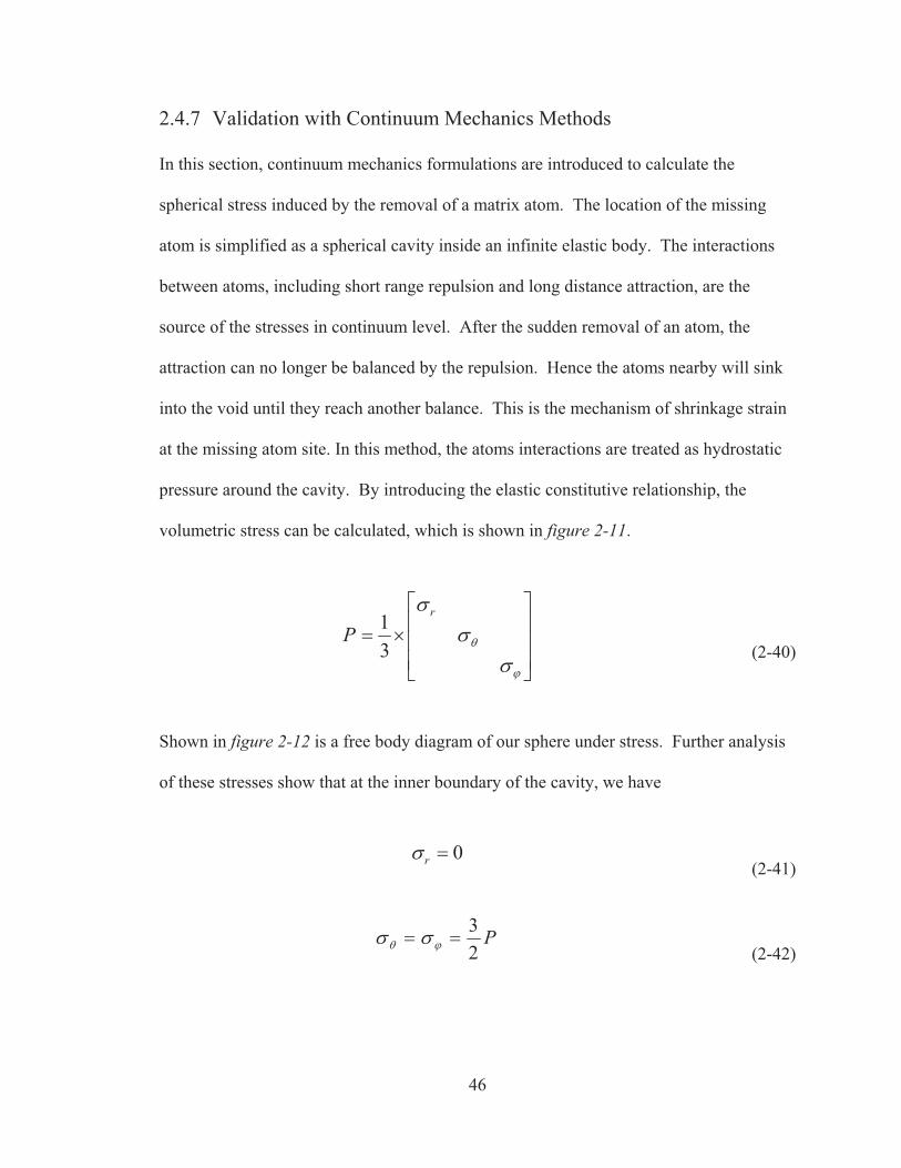
46
2.4.7 Validation with Continuum Mechanics Methods
In this section, continuum mechanics formulations are introduced to calculate the
spherical stress induced by the removal of a matrix atom. The location of the missing
atom is simplified as a spherical cavity inside an infinite elastic body. The interactions
between atoms, including short range repulsion and long distance attraction, are the
source of the stresses in continuum level. After the sudden removal of an atom, the
attraction can no longer be balanced by the repulsion. Hence the atoms nearby will sink
into the void until they reach another balance. This is the mechanism of shrinkage strain
at the missing atom site. In this method, the atoms interactions are treated as hydrostatic
pressure around the cavity. By introducing the elastic constitutive relationship, the
volumetric stress can be calculated, which is shown in figure 2-11.
���
�
�
���
�
�3�
9
:
��
� r
P31
(2-40)
Shown in figure 2-12 is a free body diagram of our sphere under stress. Further analysis
of these stresses show that at the inner boundary of the cavity, we have
0�r� (2-41)
P23
�� 9: �� (2-42)
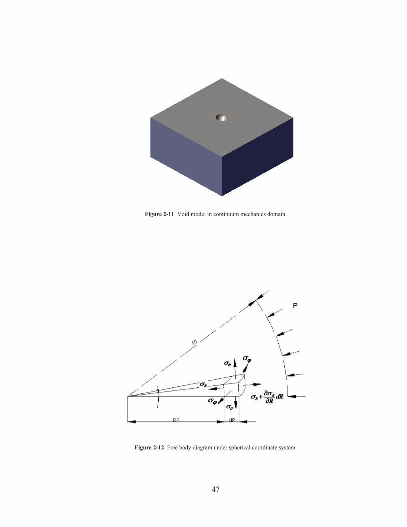
47
Figure 2-11 Void model in continuum mechanics domain.
Figure 2-12 Free body diagram under spherical coordinate system.

48
By Hooke's Law in spherical coordinates, we have
Ev
Ev r :
:��8 �
��1
(2-43)
where E is Young's modulus and 1 is Poisson's ratio. Volumetric strain from the strain of
our sphere in the : direction can be obtained by
9: 8888 ��� rv (2-44)
Applying equations (2-40) to (2-44), the spherical stress is calculated to be -3932.57MPa,
which is about 20% smaller than the virial stress P = -4932.38 MPa. As stated in the
previous section, in continuum mechanics, stress is defined as the internal force intensity
across an imaginary face. It doesn’t consider the particles that cross over the boundary.
While in molecular dynamics, virial stress measures the momentum change in a definite
group of particles. Only when the density change is negligible can the virial stress be
approximated to be Cauchy stress. In this example, a reduction factor between atomistic
and macroscopic scale will be needed to precisely consider the bulk modulus difference
in between atomic scale method and continuum mechanics method. However,
considering the small density of vacancies in the total lattice sites, Cv/Ca 1 the
vacancy relaxation factor can be safely estimated to be 0.12~0.15 in most cases. [59]
2.4.8 Conclusions
Using LAMMPS molecular dynamics simulator with the Embedded-Atom Method, we
simulated an aluminum lattice at 533K. We outputted atom positions and virial stresses

49
for a particular atom and its first-nearest neighbors. That atom was then removed, and
we used the change in positions to calculate the volume strain due to the creation of a
void. We also calculated the volumetric strain induced spherical stress with continuum
mechanics constitutive. The comparison of mechanical stress and virial stress shows that
a reduction factor is needed in order to bridge material modeling methods applicable in
atomic scale to macroscale.

50
For a metallic system under electrical load, effectively describing the electromigration
process at the macroscale requires quantitative knowledge of vacancy diffusivity in
lattice and grain boundaries, grain coarsening properties, and void flux and formation
mechanisms at the microscale, just to name a few. Additionally, knowledge of surface
energies for specific orientations of Sn’s lattice is a particularly important piece in the
characterization of the behavior of solder joints and thin films undergoing
electromigration. These energies provide an additional driving force for preferred
orientation growth of thin films and it has been shown experimentally that �Sn prefers its
(100) surface when grown on Si(111). [60] Surface energies of certain lattice
orientations are also a major component in determining the morphology and stability of
Surface Energies and Adatom Diffusivity
“Madam, I swear I use no art at all.”

51
voids that develop in thin film interconnects under electromigration conditions. [61][62]
In addition, diffusion of adatoms on these void surfaces control the overall void flux, with
movement highly dependent on anisotropy of diffusivity and direction of the electric
current. [63]
We can aid in the determination of such surface properties, normally computed
experimentally, through the use of molecular simulation. Rare-event methods are
available specifically for simulating diffusive processes in solid systems—typically slow
at simulation timescales—and can be used with relative efficiency on workstation-grade
computers or small computing clusters. [33][35][64] One technique, Henkelman’s Dimer
method, has been used to calculate activation energies and attempt frequencies of Al
adatom diffusive mechanisms with an EAM potential. [65] These compare well to ab
initio calculations using the Nudged Elastic Band method and require many fewer
potential force evaluations, without knowledge of the initial and final states of the
system. In another work, they were able to show preference of multi-atom processes in
simulated epitaxial growth of Al and Cu over long time scales. [66] Molecular simulation
also aids in the prediction of surface energies. Zhang, et al. have used the MEAM
potential to successfully calculate surface energies for various FCC and BCC metals, and
predicted lowest energy surfaces in agreement with experimental results. [67][68]
In the present chapter, we combine an MEAM potential for Sn and the Dimer method in a
quantitative study, to characterize the surface energies of �Sn and determine adatom
diffusivities for �Sn’s lowest energy surface. To our knowledge at the time of
publication, this work is the first study on the calculation of �Sn surface energies and
52
surface diffusion. This chapter continues with the details of our simulation setup in
Section 3.1, describing the properties of the simulation cell for surface energy calculation
and Dimer method simulations. Next, results from the surface energy calculations,
Dimer simulations, and diffusivity computations are presented and analyzed in Section
3.2. We offer concluding remarks in Section 3.3.
3.1 Simulation Details
In creating the surfaces for our surface energy calculation, the solid lattice was rotated so
its surface normal vector was perpendicular to the z-axis of the simulation cell. The
system was periodic in the x and y axes and the z height fixed. This allowed for the
creation of a two-surface slab. The thickness of the slabs was such that the two surfaces
did not interact with one another. Typically, this is a value greater than twice the
potential cutoff—ours often surpassed this and was dependent on the spacing between
periodic Miller planes in the simulation cell z-direction. We use equation (2-26) to
compute the surface energy relative to the bulk. A mathematically equivalent form is
used by Zhang et al. [67][68]
While the static (near 0K) system and relationship in equation (2-26) offer a
straightforward way to compute excess surface energies from molecular simulation, one
might consider other choices for the quantitative comparison of unlike material surfaces.
To unite the many relations and perceived inconsistencies in units of surface energy,
Zhao, et al. proposed the extension of the bond-order-length-strength (BOLS) correlation
that quantifies a volume-based energy density and incorporates the effect of temperature.
[69] Key components here are the representation of atomic bond contraction of under-

53
coordinated surface and near-surface atoms, thermal expansion of the lattice, and their
resulting effect on bond strength. For a more detailed investigation of surface energetics,
the work of Zhao et al. may be considered.
For our dimer simulations, the simulation cell consisted of a 4x-4y-6z block of �Sn
lattice with a single Sn adatom on the (100) surface. This surface is parallel to the YZ
plane and the cell is periodic in these directions. A total of 217 atoms made up the
system, governed by the MEAM potential with a cutoff of 4.5Å. Initially, an adatom was
placed at random on the (100) surface and allowed to equilibrate to a low energy
configuration using molecular dynamics. We presumed (and confirmed visually) that the
adatom was now seated in a low energy pocket on the (100) surface. From this initial
configuration, the dimer searches were carried out. Atoms within a distance of 8.7Å of
the adatom are allowed to move, shown in figure 3-1. Before starting the search, the
movable atoms close to the adatom were all displaced by a value between -0.2 and 0.2Å,
drawn from a Gaussian distribution, increasing the dimer’s ability to locate different low
lying saddle point configurations. Once a saddle point configuration was found, the
dimer was marched back along the lowest curvature mode to verify that it ended up in the
initial minimum region. In table 3-1are the parameters used in the dimer saddle point and
minimum searches. The energy of the saddle point, minimum region, and periodic points
along the minimum energy path (lowest curvature mode) were saved. All atoms in the
simulation are included in determining the specific energy of a configuration.
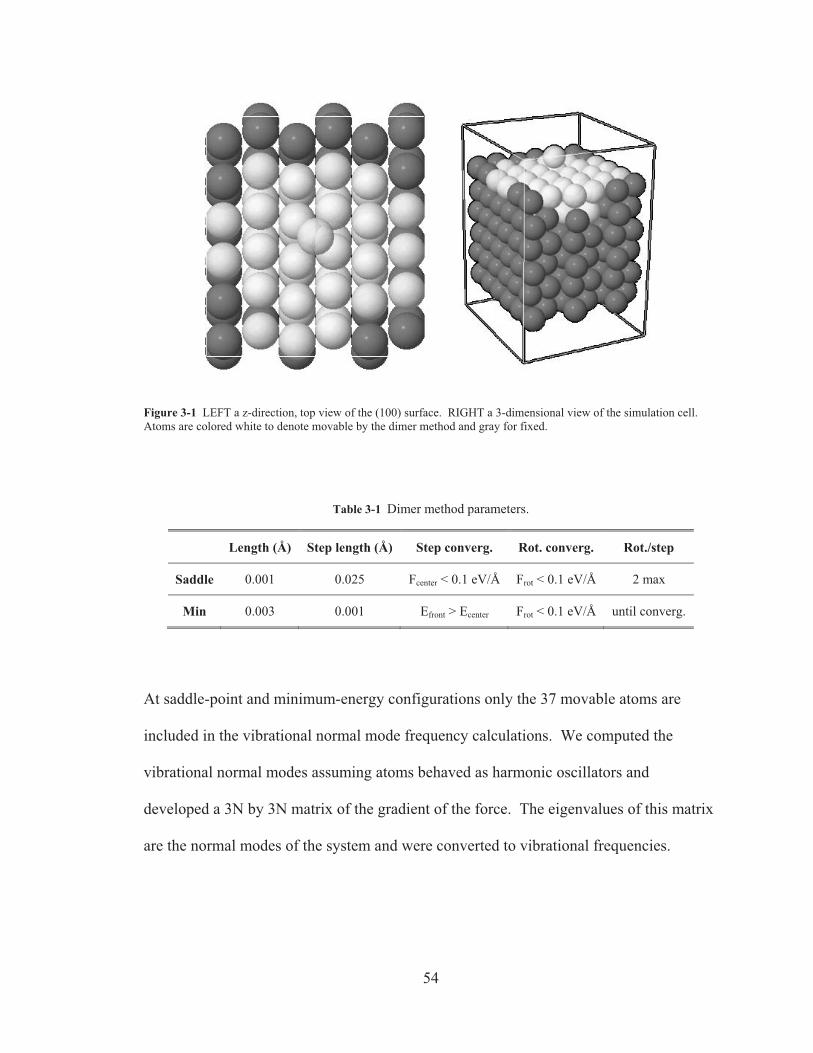
54
Figure 3-1 LEFT a z-direction, top view of the (100) surface. RIGHT a 3-dimensional view of the simulation cell. Atoms are colored white to denote movable by the dimer method and gray for fixed.
Table 3-1 Dimer method parameters.
Length (Å) Step length (Å) Step converg. Rot. converg. Rot./step
Saddle 0.001 0.025 Fcenter < 0.1 eV/Å Frot < 0.1 eV/Å 2 max
Min 0.003 0.001 Efront > Ecenter Frot < 0.1 eV/Å until converg.
At saddle-point and minimum-energy configurations only the 37 movable atoms are
included in the vibrational normal mode frequency calculations. We computed the
vibrational normal modes assuming atoms behaved as harmonic oscillators and
developed a 3N by 3N matrix of the gradient of the force. The eigenvalues of this matrix
are the normal modes of the system and were converted to vibrational frequencies.

55
3.2 Results and Discussion
3.2.1 Surface Energy Calculation for �Sn
We calculated excess surface energies of the (100), (110), (101), (111), (210), and (201)
un-relaxed surfaces for �Sn using the relation shown in equation (2-26) and a simulation
setup described in Section III. Results from these calculations are shown in table 3-2,
along with results from FCC surface energy calculations for Cu, Ag, and Al from Zhang
and co-workers. [19] It is straightforward to identify the lowest energy surface for each of
these elements—for Cu, Ag, and Al in an FCC crystal structure the lowest energy surface
is (111), while for �Sn our calculations show that (100) is the lowest energy surface. For
cubic structures, the (101) surface is equivalent to the (110) surface, as is (210) and (201).
Table 3-2 Surface energies �s of �Sn, Cu, Ag, and Al with respect to Miller plane orientation. Cu, Ag, and Al are reproduced from [19].
�s (eV/A2)
hkl �Sn Cu Ag Al
100 0.0497 0.1030 0.0795 0.0561
110 0.0622 0.1024 0.0765 0.0606
101 0.0569 -- -- --
111 0.0646 0.0879 0.0681 0.0386
210 0.0671 0.1069 0.0792 0.0666
201 0.0684 -- -- --

56
3.2.2 Surface Diffusion on (100)
Dimer searches were conducted starting from a low energy configuration of our adatom
(100) surface system, equilibrated via low temperature molecular dynamics. The dimer
searches provide information about the saddle point and minimum configurations for a
given mechanism, and with this data we computed the theoretical tracer diffusivity for
each mechanism found.
In our system a large number of configurational degrees of freedom exist, and we rely on
the dimer method to seek out and find the many possible low lying saddle points
available to the system as it undergoes some diffusive transition. More than one
thousand searches, starting with random orientations of the dimer, converged to only
three types of mechanisms. The first two involved the adatom moving across the surface
in a hop mechanism. The third was a variety of different movements of the surface
atoms, where atoms far removed from the adatom would “pop-up” out of the surface
slightly. These would lead the system to a saddle point, as well as back to the initial
minimum, but a second minimum was simply a partially raised surface atom and no
movement of the adatom. Therefore, we considered only mechanisms in which the
adatom moved. With this restriction, we found only the two hopping mechanisms
contribute to adatom movement.
It is fairly straightforward to enumerate the saddle points a diffusing adatom would
encounter hopping across the (100) face of a �Sn lattice. Figure 3-2 illustrates the (100)
surface of �Sn in an energy map, created by rasterizing the surface with an atom at a
distance of 2.0Å above and recording the energy. The high energy ion-core locations are

57
shown in red, while the low energy pockets are shown in blue. Referring to this figure, it
is quite clear where the saddle point for a single atom diffusion transition might be
located. We have labeled the energy map with the location of the common minimum
and two unique saddle points found in our dimer method searches and minimum energy
path traces.
Figure 3-2 Energy maps of the �Sn (100) surface. Left. Red denotes a higher energy (ion cores), blue denotes lower energy. Right. Diamonds are respective saddle point locations of the adatom, white circles are minima locations.
The two mechanisms found were a relatively simple movement of the adatom from one
minimum energy pocket to the next closest minimum energy pocket. Looking at the
(100) plane in figure 3-2, these translate to a z-direction movement (lattice c-direction) of
the adatom and a y-direction movement (lattice a-direction) of the adatom. If a system
started at one of the specified minimum configurations (white circles in figure 3-2), it
could either move in the positive or negative c-direction through a saddle point (indicated
by the red diamond) or in the positive or negative a-direction (indicated by a green
diamond). Specific data from these mechanisms is shown in table 3-3 and the energy
values along the minimum-energy path are shown in figure 3-3 as red and green curves.

58
Figure 3-3 Energy values along the minimum energy path for the given mechanisms. Values along the reaction coordinate are corrected to a baseline value of the minimum energy configuration—both mechanisms begin and finish at 0eV. Diamonds denote energies corresponding to saddle point configurations.
With the results of the dimer search, vibrational analysis, and displacement
measurements, we computed the theoretical tracer diffusivity of the adatom for each
mechanism at a temperature of 300K using equations (2-21), (2-22), and (2-23).The
factor & for these diffusivities is taken to be 1 because the mechanisms move the adatom
in only one dimension. Shown in table 3-3 are our values for attempt frequency,
activation energy, and diffusivity at 300K.
Table 3-3 Mechanism data. Respectively, the adatom direction, mechanism activation energy, attempt frequency, distance the adatom traveled, and tracer diffusivity at 300K are specified.
Mechanism EA (eV) ��(THz) l (Å) D (10-06 cm2/s) 300K
c-dir 0.1493 1.17 3.23 1.893
a-dir 0.1138 0.745 2.96 3.994

59
Ratsch and Scheffler report that for Ag adatom on an Ag (111) surface, as the number of
degrees of freedom considered in the vibrational normal mode frequency calculation
increase, the attempt frequency decreases. [38] For their largest normal mode frequency
calculation, they compute an attempt frequency value of 0.71THz, where 3N=99 and N is
the number of atoms included. This result is similar to our calculations shown in table
3-3. In addition, their activation energy was calculated at 0.082eV for an adatom
hopping on the (111) surface of Ag, known to be FCC’s lowest energy surface, and
compares on a similar scale to our measurements for an adatom hoping on �Sn’s lowest
energy surface. In contrast, Henkelman’s results for Cu and Al adatom activation
energies on higher energy (100) surfaces are 2 to 3 times larger than our values. [65][66]
Additional values of the theoretical tracer diffusivity for each mechanism are computed
via the previously mentioned relations and an Arrhenius plot of diffusivity vs.
temperature is shown in figure 3-4. The y-axis is in logarithmic scale and the x-axis is in
inverse temperature scale. Here, �Sn’s lattice anisotropy clearly plays a role in the
directional diffusivity. At high temperatures however, this difference is less pronounced.

60
Figure 3-4 Arrhenius plot of diffusivity with respect to inverse temperature.
3.3 Conclusions
Our calculations of surface energies of various low index Miller planes of the �Sn phase
indicate that the (100) surface has the lowest excess surface energy. A preference for the
(100) surface has been shown in experiment, and our results using the MEAM potential
confirm that from a surface energy minimization standpoint, the (100) surface preference
should be exhibited in most epitaxial growth experiments. In addition, we also provide a
list of surface energies for use in studies of void migration in �Sn. We have also shown
results for the diffusivity of a Sn adatom on a �Sn (100) surface via theoretical and
numerical methods. The adatom on the (100) surface exhibited hopping diffusion
mechanisms in the a-direction and c-direction of the lattice. Attempt frequencies and
activation energies were slightly different for each type of system. The differences in

61
each case correspond to unique behaviors of diffusivity with respect to temperature and
directionality of diffusion.
In all our dimer simulations, we did not observe any concerted atom rearrangement like
that of the Cu and Al (100) surfaces that Henkelman simulated. We believe this is most
likely due to the apparent layering of the �Sn lattice in the [100] direction. An FCC
lattice exhibits a tight, alternating packing in the [100] direction for successive (200)
lattice planes, providing a physically and energetically deeper pocket for an adatom to sit
on its surface. This may cause mechanisms involving concerted rearrangements to have
activation energies similar to those involving adatom hopping. While for �Sn, successive
(200) surfaces in the [100] direction appear shifted with respect to FCC. Atoms in the
faces of �Sn’s structure fall closer in line with its corner atoms along the [100] direction,
creating sheet-like layers of atoms. Accordingly, an adatom on the energetically
smoother (100) layer of �Sn may move much more freely by hopping than taking part in
surface atom rearrangement.
62
Diffusivities for different types of grain boundaries and a description of the boundary
behavior with temperature, are critical in modeling microstructure evolution. Few
experimental diffusion studies have been conducted on Sn grain boundaries, but
activation energies obtained from experimental work on diffusion in the bulk Sn have
been determined. They span a range of values. [9][70][71][72] Sun and Ohring suggest
that some authors who report low activation energies may in fact be unknowingly
measuring grain boundary diffusion. [72] Results from a significant number of bulk Sn
studies are compiled in their work and reveal that grain boundary diffusion activation
energies fall in a distinct range. In a follow-up study on polycrystalline Sn, Singh and
Ohring measure grain boundary diffusivity at low and high temperatures. [9] Their high
Grain Boundary Structure and Self-Diffusivity
“This above all: to thine own self be true.”
63
temperature results match well with a cited second study on grain boundary diffusion and
the values from Singh and Ohring's work are used in many studies of solder joint
damage. One example is a finite-element simulation incorporating �Sn, Ag, and Cu
diffusivities providing overall “solder joint diffusive activation energies” computed from
time-to-failure measurements. [73]
In the present chapter, we employ molecular dynamics (MD) simulation to determine
grain boundary diffusivity of specific �Sn grain boundaries. Although a significant
amount of simulation work has been completed on grain boundaries in various materials
and by a variety of methods, we believe, at the time of publication, this is the first to
study �Sn grain boundaries. [41][64][74] We compare our results of diffusivities
calculated in grain boundary structures to Singh and Ohring’s average �Sn grain
boundary diffusivity and activation energy. Recent work by Telang and Bieler show the
consumption and growth of particular grains of Sn when a polycrystalline sample is
subjected to stress and high temperature anneal. [17][75] The specific grain boundary
structures that persist in their work form the basis for the range of structures we study
here. Notably, they see an increase in the number of (101) and (301) symmetric tilt grain
boundaries present in their samples after separate stress and heat trials. [17] We
construct the first of these boundaries in simulation, and include other structures that are
of a similar grain boundary character. The range of grain boundaries studied can describe
an average diffusivity one might expect in a polycrystalline sample, yet also exhibit
individual behavior worthy of investigation.

64
This chapter follows with our simulation details in Section 4.1 as we outline our specific
grain boundary structure choices and their minimization. We then present results with
discussion in Section 4.2 and follow up with conclusions in 4.3.
4.1 Simulation Details
�Sn phase grain boundaries in this work are created with custom Java code using the
Etomica API and modeled using the modified embedded atom method (MEAM) with
MD simulations conducted in the LAMMPS molecular simulation package. [58][76]
The process of minimization of the grain boundary is done in two steps. First, near 0K
the two grains move independently in x, y, and z-directions via molecular dynamics, their
respective atoms all having the same average force each time step. This step is shown in
figure 4-1-1. An investigation in NiAl alloy grain boundaries by Mishin and Farkas
employed the �-surface technique to map out the energy surface created by the two static
moving grains. [77] We do not employ this technique; however our 0K minimized
structures do find lower energy configurations relative to their initial structure. Once a
minimum energy structure has been found, the system is then equilibrated at the desired
production run temperature, figure 4-1-2. Here, atoms in the bottom grain within twice
the potential cutoff distance of the bottom edge of the structure are fixed and atoms in the
top grain within twice the potential cutoff distance of the top edge of the structure are
given an average force in the x, y, and z-directions. This creates a floating boundary at
the top of the box and allows the system to reach an average zero pressure over 100
picoseconds. Following these steps, the floating boundary is now fixed and the grain
boundaries are simulated between 2 and 4 nanoseconds, figure 4-1-3.

65
Figure 4-1 (1) Minimization (near 0K-MD), (2) Equilibration, and (3) Production structures. Actual simulation cells are 3-dimensional and periodic in x and y-directions.
4.2 Results and Discussion
With MD we simulated five medium to high energy �Sn symmetric tilt grain boundaries.
Specifically, boundaries with grains that share the (101), (201), (401), (310), and (410)
Miller planes at their interface. For each grain boundary, we computed the excess
potential energy at 300K from an average value sampled over the course of our molecular
dynamics production runs. We also computed �GBDGB during the simulations and
estimated the value of �GB, the grain boundary diffusive width, at temperatures from
300K to 450K. From here we calculated DGB for all boundaries in the temperature range
and examined more closely directional diffusion in the interface of the (401) grain
boundary.
4.2.1 Grain Boundary Excess Potential Energies
An often adequate measure of the order at the grain boundary interface and a
characteristic of its transport behavior is the excess potential energy of a grain boundary.
Outlined in a previous section, this quantity is the extra energy resulting from the low

66
coordination of interface atoms. Shown in table 4-1are computed excess energies of the
five grain boundaries studied in this work. It is clear from these calculations that,
depending on the Miller plane chosen, there exists a different degree of lattice mismatch,
corresponding to an excess energy value. For the (101), (201), and (401) grain
boundaries, the excess grain boundary energy decreases with increasing h index.
However, for the (310) and (410) planes, the energy slightly increases with increasing h
index.
Table 4-1 Excess Interfacial Potential Energies (mJ/m2) at 300K.
GB (101) (201) (401) (310) (410)
300K 1089.68 364.08 198.98 338.76 343.44
4.2.2 Grain Boundary Width-Scaled Diffusivity (�GBDGB)
Results from squared displacement samples are shown in figure 6. Here we plot in
Arrhenius form the scaled diffusivity, �GBDGB, versus temperature. In addition to data
from our grain boundary simulations, experimental scaled diffusivity values from Singh
and Ohring are shown as dark lines. [9] These lines represent the two different
experimental relationships used to analyze the concentration profiles of Sn radiotracer in
polycrystalline thin films. Arrhenius parameters for the experimental data plotted in
figure 4-2 are shown in table 4-2.

67
Table 4-2 Arrhenius properties calculated from experiment in ref [9].
300K to 350K 350K to 450K
DGB (10-8cm2/s) 1.45 (300K) 6.34 (350K)
�GB (10-8 cm) 5.0 (assumed)
EA (eV) 0.50 +/- 0.04 0.4245
D0 (10-2cm2/s) 490 +1560/-370 8.3
Figure 4-2 Arrhenius plot of scaled diffusivity vs. temperature. Points are results for various symmetric tilt grain boundaries simulated in this work. Dark lines are experimental data from Singh and Ohring. [9] Error bars represent standard deviation of three independent simulations and computations of �GBDGB .
68
We can see from figure 4-2 that the �GBDGB values for the simulated grain boundaries,
with the exception of the (401) grain boundary, behave in a trend relative to their excess
potential energies. For example, the (101) grain boundary exhibits the highest excess
energy and the highest width scaled diffusivity. When compared to experiment at low
temperature, the simulated boundaries show good agreement with experimental data.
Magnitudes of the width scaled diffusivity at low temperature are all within the error
reported in [9] and reproduced in table 4-2. An argument could be made about the large
discrepancy in slope (diffusive activation energy) at low T, however when considering
statistical uncertainty the slopes appear similar for many of the grain boundaries. This
point will be discussed later in our analysis of DGB. Continuing the comparison to higher
temperatures, all our boundaries fall, at most, within one order of magnitude of
experimental values and show a similar trend in slope. Further comparison of
diffusivities is done by calculating DGB using values of �GB for each grain boundary at a
range of temperatures.
4.2.3 Grain Boundary Width Calculation
To investigate possible changes in interface width with particular grain boundaries and/or
temperature, we calculated planar profiles of diffusivity and structure in planes parallel to
the grain boundary interface. For every grain boundary, at temperatures from 300K to
450K, diffusive and structural widths were calculated using methods outlined in the
previous section. Shown below are two figures representing results from calculations of
�GB. The first, figure 4-3, presents planar diffusivity profiles of the five grain boundaries
studied in this work. We have selected temperatures of 300K and 450K to display.

69
Figure 4-3 Planar diffusivity for various grain boundaries at 300K (left) and 450K (right). Note the different scales for each temperature, but similar scales for z. Lines are guides for the eye.
As shown in figure 4-3 for a temperature of 300K, we see an increase in planar
diffusivity and an increase in diffusive width with increasing grain boundary energy.
Here, the (401) boundary exhibits a relatively high diffusivity with a narrow width. For
450K, the (401) grain boundary again displays similar behavior, while the other
boundaries now have a diffusivity within the same order of magnitude. Also, at higher
temperature, the boundaries are shown to maintain their diffusive widths.

70
In addition to measuring the width via planar diffusion, we investigated the structural
behavior of each grain boundary. Figure 4-4 shows plots of the squared planar structure
factor for each grain boundary. Each illustrates a change in the boundary’s structure with
temperature. The type of change varies between grain boundaries, but we note for the
(101) and (201) grain boundaries, as we approach 450K the disordered structure at the
interface grows in a width-wise fashion. For (401) and (410) the width is maintained, yet
the amount of disorder changes with temperature. In figure 4-5, we include simulation
snapshots for the (101) grain boundary at temperatures of 300K and 450K. For views
oriented parallel to the grain boundary tilt axis, we see a slight decrease in ordering
(increase in width) at the lattice-interface plane when comparing 300K to 450K.

71
Figure 4-4 Square planar structure factor vs. z-axis plane for the five grain boundaries studied. Colors are different temperatures. Blue-300K, Green-350K, Orange-400K, Red-450K. Error bars represent the standard deviation of |S(k)|2 in five snapshots from an MD run.

72
Figure 4-5 TOP and BOTTOM are snapshots of the (101) GB at 300K and 450K, respectively. LEFT is looking parallel to the grain tilt axis and at RIGHT looking perpendicular.

73
Figure 4-6 Diffusive (open points, left) and structural widths (filled points, right) versus temperature for the five grain boundaries studied. Lines are guides for the eye. Black lines is the diffusive width used in ref [9].
Diffusive and structural widths for each grain boundary are compiled and plotted versus
temperature in figure 4-6. We also include the value used in the experimental work, �GB
= 5.0Å. From figure 4-6 we can see that each grain boundary exhibits different widths.
While not as distinct as the magnitudes of diffusivity, the high energy grain boundary
shows the largest width, medium energies show slightly smaller widths, and the low
energy (401) shows the smallest width. Contrasting the two types of analysis, diffusive
74
and structural, we see that the diffusive width remains relatively constant while the
structural is more dynamic and increases with temperature for a few of the boundaries.
For the two boundaries ((101) and (201)) that show slight increases in their structural
width with temperature, we also observe a large degree of disorder at the interface.
Compared to the other plots in figure 4-4, these two boundaries exhibit almost no
structure when compared to �Sn’s bulk lattice. The extreme of this scenario is evidence
of a large increase in grain boundary width and a transition to liquid-like disorder with an
increase in temperature at points below the material’s bulk melting point. This is referred
to in literature as a “pre-melting” transition. Previous work by Keblinski et al. on
molecular dynamics simulations of FCC Pd grain boundaries asserts the existence of
grain boundary pre-melting at temperatures below the bulk melting temperature. [40]
Their high energy boundaries undergo a transition to a confined liquid structure at a
critical temperature dependent on boundary energy. Evidence of this liquid structure
transition is given by a change in diffusion activation energy and a diffusivity that
increases to a value close to the liquid value at the melting temperature. An earlier study
by Ciccotti et al. of Lennard-Jones (310)-05 grain boundaries found only partial
structural disorder in this boundary as the melting point is approached. In their analysis,
they compute a grain boundary diffusivity for their system near the melting point that is
below the super-cooled liquid value at the same temperature. [42] In another study by
Suzuki and Mishin, where Cu (210)-05 and (310)-05 grain boundaries were simulated up
to the melting point, they did not see any evidence of pre-melting in their systems. They
do note however, that all the grain boundaries collapse on a common self-diffusivity
close to the melting temperature. [41] Similar to reports in literature, the various studies

75
of structure and dynamics in our grain boundaries do not explicitly show that pre-melting
is occurring for �Sn. We do see disordered interfaces develop for the (101) and (201)
grain boundaries and they remain stable throughout the temperature range studied in this
work. While this may suggest the notion of pre-melting in our boundaries, the foundation
of its existence is dependent on a change in slope of the grain boundary diffusivity. DGB
at high temperature must also present a value close to liquid self-diffusivity as the
melting point is approached. Upon further analysis, detailed in the next section, we see
no change in the slope of DGB as temperature is increased and magnitudes that do not
approach the liquid diffusivity as the melting point is approached. We can therefore say
that although some of our simulated interfaces show disorder, none exhibit the pre-
melting phenomenon.
4.2.4 Resolving the Grain Boundary Diffusivity (DGB)
Using values of the diffusive width (�GB) for each temperature and grain boundary type,
we now resolve DGB for each grain boundary, and remove the effect of �GB's variation
with grain boundary type on �GBDGB previously shown in figure 4-2. Here, the specific
grain boundary self-diffusivity, DGB, for each type studied in this work is shown in figure
4-7. The standalone data in figure 4-7 is the (401) grain boundary. It now shows its true
diffusivity in comparison to the other simulated grain boundaries. Although the width is
small, the low energy (401) boundary exhibits fast, low activation energy, diffusion. This
behavior is given further study in the next section. Singh and Ohring report values of
DGB using �GB = 5.0Å to adjust their experimentally measured values of �GBDGB. This is
also plotted in figure 4-7. Compared to figure 4-2 and relative to Singh and Ohring’s

76
reported values, we see similar trends from the (201), (310), and (410) grain boundaries.
For the (101) grain boundary, the magnitude of DGB has shifted slightly lower relative to
the experimental results. Our low temperature values, 300K to 350K, still fall within the
error in Singh and Ohring’s measurements, outlined in table 4-2 (though no error is listed
for high temperature), and all our values are still within one order of magnitude of
experiment. It is important to mention finally that using any value larger than �GB = 5.0Å
with the experimental results will decrease the gap between it and simulation. The
authors of ref. [9] do not mention the significance of this value for �Sn, although in other
works, when used in analytical expressions, it is shown to match experimental results in
higher melting point materials, such as Ag. [78]
Table 4-3 Arrhenius Properties of Simulated Grain Boundaries from weighted least squares fit, 325K to 450K
GB (101) (201) (401) (310) (410)
DGB-300K (10-8cm2/s) 2.11 1.55 10.9 0.914 0.700
EA (eV) 0.263(4) 0.295(5) 0.10(1) 0.22(5) 0.274(7)
D0 (10-4cm2/s) 2.9(4) 6(1) 0.08(5) 2.2(8) 40(2)
The slopes of simulation data from 350K to 450K show good agreement with experiment.
At low temperatures of 300K and 325K however, average values from multiple
simulations create a low-slope region. This behavior is similar to that in figure 4-2 and is
maintained even after removing the influence of width. While the amount of error shows
that statistically, these points may have a slope that is similar to higher temperature data,
we’ve restricted the analysis of DGB to values simulated at temperatures of 325K to 450K.

77
We believe the large error at 300K arises from poor sampling because of the timescale
constraints of molecular dynamics. A weighted least squares fit is applied to figure 4-7
diffusion data in this temperature range to calculate Arrhenius parameters for each grain
boundary. These are shown in table 4-3.
Figure 4-7 An Arrhenius plot of grain boundary diffusivity vs. temperature. Shown as colored points are various symmetric tilt grain boundaries simulated in this work. Dark lines are experimental data from Singh and Ohring. Error bars represent standard deviation of three or more independent simulations.
4.2.5 Analysis of In-plane Directional Diffusivity
In figure 4-7 and table 4-3, we see a contrast in slope of the (401) grain boundary when
compared to other low DGB grain boundaries (e.g. (310), (410)). While of low excess
potential energy and therefore high atomic coordination at the interface, the activation
energy of diffusion in this grain boundary is low. This duality is indicative of possible

78
channel structures forming at the interface in a single direction. [30] Accordingly, we
investigated the development of any anisotropy in diffusivity in the plane of the grain
boundary interface. Shown in figure 4-8 are plots of (h10) and (h01) grain boundaries
and their respective �GBDGB component values. For both plots, diffusion in the direction
parallel to the grain tilt is shown as open points and diffusion perpendicular to the grain
tilt is shown as filled points. For the (310) and (410) grain boundaries, shown in the left
plot, self-diffusion in either direction is essentially equivalent. For the (101), (201), and
(401) however, as the h index of the grain boundary is increased, a degree of anisotropy
in the diffusion coefficient develops.
If we focus on the (401) grain boundary, we can see a high degree of directional
diffusivity. This is also evidenced in simulation snapshots, shown below in figure 4-9.
By inspection, the structure of the (401) grain boundary is much more evident in a view
down the grain tilt axis ([010]), as shown in the parallel view direction of figure 4-9.
Conversely, the perpendicular view direction of this figure shows a thin interface with
disordered atoms.
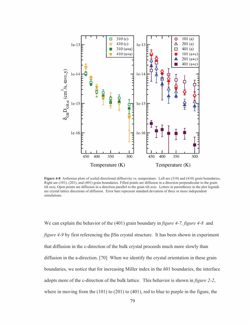
79
Figure 4-8 Arrhenius plots of scaled directional diffusivity vs. temperature. Left are (310) and (410) grain boundaries, Right are (101), (201), and (401) grain boundaries. Filled points are diffusion in a direction perpendicular to the grain tilt axis; Open points are diffusion in a direction parallel to the grain tilt axis. Letters in parentheses in the plot legends are crystal lattice directions of diffusion. Error bars represent standard deviation of three or more independent simulations.
We can explain the behavior of the (401) grain boundary in figure 4-7, figure 4-8 and
figure 4-9 by first referencing the �Sn crystal structure. It has been shown in experiment
that diffusion in the c-direction of the bulk crystal proceeds much more slowly than
diffusion in the a-direction. [70] When we identify the crystal orientation in these grain
boundaries, we notice that for increasing Miller index in the h01 boundaries, the interface
adopts more of the c-direction of the bulk lattice. This behavior is shown in figure 2-2,
where in moving from the (101) to (201) to (401), red to blue to purple in the figure, the
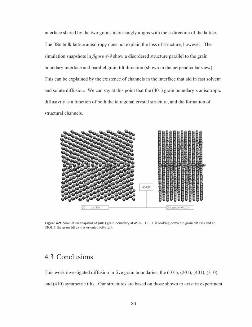
80
interface shared by the two grains increasingly aligns with the c-direction of the lattice.
The �Sn bulk lattice anisotropy does not explain the loss of structure, however. The
simulation snapshots in figure 4-9 show a disordered structure parallel to the grain
boundary interface and parallel grain tilt direction (shown in the perpendicular view).
This can be explained by the existence of channels in the interface that aid in fast solvent
and solute diffusion. We can say at this point that the (401) grain boundary’s anisotropic
diffusivity is a function of both the tetragonal crystal structure, and the formation of
structural channels.
Figure 4-9 Simulation snapshot of (401) grain boundary at 450K. LEFT is looking down the grain tilt axis and at RIGHT the grain tilt axis is oriented left/right.
4.3 Conclusions
This work investigated diffusion in five grain boundaries, the (101), (201), (401), (310),
and (410) symmetric tilts. Our structures are based on those shown to exist in experiment
81
and those that exhibit sufficient motion for squared displacement calculations during
molecular dynamics simulations at temperatures of 300K to 450K. We find that �GBDGB
is not the most effective way to describe the transport behavior of these grain boundaries.
One must also investigate the boundary’s interface width.
By determining the structural and diffusive widths of the interfaces of the grain
boundaries, we can resolve the specific grain boundary diffusivity, DGB, for each type.
The diffusive width is used to back out DGB from the simulation quantity �GBDGB, while
the structural width analysis reveals information about possible changes in structural
order of the grain boundaries. Calculation of the parameter �GB shows that a grain
boundary with higher energy will exhibit a larger width. We also show that this width
remains fairly constant at temperatures from 300K to 450K. Specifically for the (101)
grain boundary, structural and diffusive widths reveal a highly diffusive, disordered
structure in comparison to other boundaries in this work. The (201) grain boundary
exhibits this to a lesser extent. Parameters necessary to formulate an Arrhenius relation
for each grain boundary, such as activation energy and diffusive prefactor, are tabulated.
A directional analysis of the diffusivity in each grain boundary interface illustrates
anisotropy in diffusivity, developing as the h Miller index is increased from 1 to 2 to 4 in
(h01). Further analysis of the (401) grain boundary shows that even at low temperatures,
it is a fast diffusing interface dominated by structural channels. This is described in two
parts. We first show this by examining the slow bulk lattice diffusivity of �Sn in the
crystal’s c-direction ([001]). In this case, the lattice c-direction is perpendicular to the
axis of grain tilt ([010]) in the (401) grain boundary, lending very slow diffusion to the

82
boundary in this direction. Second, it is confirmed by inspection of simulation snapshots
and knowledge of the boundary’s excess energy. For a boundary of such low excess
potential energy compared to a bulk structure, and such high diffusivity with low
activation energy, stable structural channels must develop in the interface. We see this
disorder in only the perpendicular-to-tilt view of the grain boundary. These two
observations explain slow diffusion in the perpendicular direction of the interface, and
overall low activation energy and fast diffusion in the (401) boundary caused by
disordered channels in the parallel direction of the interface.

83
The structure of Sn, commonly microcrystalline or polycrystalline �Sn in solder joints,
allows for a range of macroscale material strength and mass diffusion regimes, both
resulting from the frequency and types of boundaries created by the �Sn grains.
[9][17][75] Many factors influence the size of the grains and amount of grain boundaries
in a joint. Current experimental work shows that solder joints exhibit varying types of
microstructure, due in part to changing solute concentration. In 2009, Seo et al.
examined Sn-xAg and Sn-xCu solder joints and found that microstructure was
significantly affected by alloy composition and cooling rate. [18] In a later but similar
work by the same authors, the time evolution of microstructure is examined during high-
temperature aging, and solute concentration is shown to affect grain growth. [79] Earlier
Solute Effects on Grain Boundary Energy and Shear Stress
“Neither a borrower nor a lender be...”

84
work by Telang et al. confirms Seo et al.’s findings. [17] For pure Sn ingots, reflowed
Sn, and solder joints with concentrations of Ag similar to that of Seo et al., they observe a
similar fine microstructure of �Sn.
Studies at an atomistic level have investigated the effect of size, cohesive energy, and
concentration of solute atoms on total grain boundary energy (EGB). In 2005, Millett et
al. showed that Lennard-Jones solute atoms of a range of sizes are more effective at
lowering EGB than atoms of various cohesive energies. [46] In fact, atoms with larger
cohesive energies increased EGB. Millett’s work also demonstrates the possibility of
solute stabilization of grain growth in nanocrystals. [48] They show that for a
nanocrystalline system of LJ atoms, at concentrations of solute atoms greater than 2.0%,
all grain growth is halted during molecular dynamics simulations of the system.
Furthermore, they compute the excess energy of the grain boundaries (difference from
the bulk structure with solute), and find that at these concentrations, the nanocrystalline
system exhibits a lower energy than the bulk single crystal counterpart.
The recent experimental studies on Ag and Cu solute effects on �Sn microstructure, solid
base of theory and simulation work, present an opportunity to use molecular simulation to
directly model a realistic system, with the goal of quantifying and explaining solute
effects at an atomistic level. In this work we use molecular dynamics simulation to
examine the effect that low-to-moderate concentrations of Ag and Cu solute atoms have
on the grain boundary energy of �Sn. The (101) symmetric tilt boundary of �Sn is
simulated with varying amounts of solute, and using the Modified Embedded-atom
method, we obtain values for the segregation enthalpy of Ag and Cu, as well as

85
respective critical excess solute amounts. We also investigate the behavior of the solute
stabilized boundaries under shear stress as a function of solute amount and compare these
to experimental and simulation work. Finally, we offer conclusions that explain some of
the behavior exhibited by the solder joints in experimental work.
We continue this chapter with an explanation of the details of our simulation setup and
data collection in Section 5.1. We then present and discuss our results of grain boundary
energy calculations and shear stress simulations in Section 5.2, and end with conclusions
in Section .
5.1 Simulation Details
In our simulations, we are modeling the (101) symmetric tilt grain boundary of �Sn, with
varying amounts of Ag or Cu solute particles randomly placed in interstitial positions
along the interface. The grain boundary with solute configurations are constructed with
the Etomica Molecular Simulation API. [76] Interactions between Sn and Ag, and Sn
and Cu are modeled with the Modified Embedded-atom method (MEAM) in the
LAMMPS Molecular Simulator. [24][58]
Similar to Chapter 4, our simulation cell is periodic in the directions parallel to the grain
boundary interface, and fixes atoms at the top of grain 1 and at the bottom of grain 2,
mimicking a bulk structure and creating a “sandwich” of movable atoms. [30] Various
quantities of solute are then randomly inserted into interstitial positions at the grain
boundary interface. The final structure is shown in figure 5-1 as a normal and expanded
view. In this type of setup it is important to equilibrate the system correctly in order to

86
obtain a grain boundary interface of minimum energy, and to simulate at an average
pressure of zero.
Figure 5-1 Typical configuration of grain boundary with its interface loaded with solute (orange). LEFT is a simulation snapshot after equilibration and RIGHT is the same snapshot with the interface exposed for clarity.
Table 5-1 Ag and Cu solute quantities and corresponding excess interfacial density.
Ns (atoms) 5 10 25 50
�s (10-3 atoms/Å2) 2.085 4.171 10.43 20.85
The process of equilibration of the grain boundary is done in three steps, followed by our
shear simulation. First, near 0K the two grains move independently in x, y, and z-
directions via molecular dynamics, their respective atoms all having the same average
force each time step. This step is shown in figure 5-2-1. Next, solute atoms are
randomly inserted at interstitial positions in the grain boundary interface. Shown in table
5-1 are the specific amounts of solute inserted and their corresponding interfacial excess

87
density. The positions of the solute atoms are then adjusted via a conjugate gradient
energy minimization, while holding the Sn atoms fixed (figure 5-2-2).
Finally, once a minimum energy configuration is found, the system is then equilibrated
for 100 ps using molecular dynamics (MD) with a Nose-Hoover thermostat and barostat
(NPT) at the desired production run temperature and with a timestep of 0.001 ps (figure
5-2-3). Here, atoms in the bottom grain within twice the potential cutoff distance of the
bottom edge of the structure are fixed and atoms in the top grain within twice the
potential cutoff distance of the top edge of the structure are given an average force in the
x, y, and z-directions. This creates a floating boundary at the top of the box and allows
the system to reach an average pressure of zero over 100 ps. During the last 50,000
timesteps (50 ps) of this step we collect our average energies of grain boundaries with
solute concentrations shown in table 5-1.
Figure 5-2 (1) Grain boundary minimization (near 0K), (2) Solute minimization, (3) NPT MD equilibration, (4) NVT MD Shear simulation. Filled arrows indicate direction of motion of the block portion. Orange circles are solute at interface. Free atoms are movable in x, y, and z directions. Actual simulation cells are 3-dimensional and periodic in x and y directions.
Following these steps, the floating boundary is fixed in the y- and z-directions, and
moved at a constant velocity of vx = 5x10⁻⁴ Å/ps in the x-direction. Initially, the free
88
atoms of the system are given an additional x-velocity profile in the z-direction to offset
the sudden shock of the moving top boundary. The initial profile is linear from (vx, z)
points of (0.0Å/ps, -40Å) to (5x10⁻⁴Å/ps, 40Å). For a system under shear, we calculate
the off-diagonal term of the stress tensor describing the stress in the direction of the shear
force and the out of plane normal. In this chapter, all shear is in the x-direction of the x-y
plane, so the desired stress is �xz. It follows that the shear strain rate is given by equation
(5-1), where vx is the shear velocity in the x direction and z is the height of the simulation
cell.
zvx���
(5-1)
Applying equation (5-1), this becomes the equivalent to a shear strain rate of �� =
6.25x10⁶ s-1, as all of our systems have a height (in z-direction) of roughly 80Å. During
the shear, systems containing various amounts solute are simulated with constant volume
(NVT) MD between 9 and 15 ns (figure 5-2) using the same timestep as in step 3. Our
simulation box remains un-deformed.
Doing work on the system in the form of shear adds energy, and for significant shear
strain rates this can have an effect on the temperature. It is customary in this case to
either compute the temperature using a non-sheared component of the velocity, or to
remove the shear effect by subtracting shear velocity based on an atom’s location
perpendicular to the shear direction (effectively removing our initial velocity profile).
[81][82] Although we are imposing a comparably low shear rate on our system, we use

89
the method of ref. [82] and subtract the shear velocity profile from our kinetic energy
calculation before computing the temperature.
5.2 Results and Discussion
Molecular dynamics simulations of the (101) �Sn grain boundary are conducted for
various temperatures and solute concentrations. The average energy of each structure
containing amounts of Ag and Cu listed in table 5-1 is determined and used with the
energy of the pure boundary to compute the enthalpies of segregation for Ag and Cu at
different temperatures. We also investigate the behavior of this boundary with 25 and 50
solute atoms under a constant shear rate. As a complement to the excess energy
calculation, measuring the boundary’s response to a steady shear and observing the yield
stress offers a way to qualitatively represent the structural stability of the boundary and
the effect of solute atoms on boundary slip.
5.2.1 Excess Enthalpy Calculations
Table 5-1 lists the four excess solute concentrations inserted into the (101) grain
boundary interface. At temperatures of 300K, 350K, 400K, and 450K, molecular
dynamics simulations were used to obtain the average energies of all the temperature-
solute amount combinations. Following the procedure outlined in Sections 2.3.1 and
2.3.2, the excess energies of the boundary with solute and the pure boundary were
computed. Employing equation (2-31), we know HEX,GB+S, HEX,GB, and �EX for each
temperature, and can solve for �HSEG, the enthalpy of segregation. In figure 5-3 we plot
HEX,GB+S, the excess energy of the grain boundary with solute, as a function of interfacial

90
excess solute concentration, �EX. At each temperature, the weighted least-squares
method was used to determine trend lines, and the slope of these lines is the solute’s
enthalpy of segregation. The first rows of table 5-2 and table 5-3 report these values.
Figure 5-3 Difference in the excess enthalpies of the solute loaded grain boundary and bulk �Sn with an equal amount of solute (HEX,GB+S) vs. excess solute concentration (�EX). Error is the standard deviation. Trend lines are fitted by a weighted least-squares analysis.
Equation (2-31) also allows for the possibility of reducing the energy of the grain
boundary with solute to a value equal to, or less than, that of the pure crystal. In figure
5-3 , the trend lines for each temperature will intersect the y-axis of the plots at or near
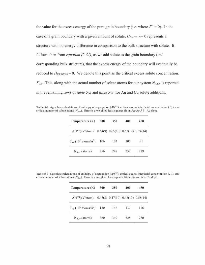
91
the value for the excess energy of the pure grain boundary (i.e. where �ex = 0). In the
case of a grain boundary with a given amount of solute, HEX,GB+S = 0 represents a
structure with no energy difference in comparison to the bulk structure with solute. It
follows then from equation (2-31), as we add solute to the grain boundary (and
corresponding bulk structure), that the excess energy of the boundary will eventually be
reduced to HEX,GB+S = 0. We denote this point as the critical excess solute concentration,
�CR. This, along with the actual number of solute atoms for our system NA,CR is reported
in the remaining rows of table 5-2 and table 5-3 for Ag and Cu solute additions.
Table 5-2 Ag solute calculations of enthalpy of segregation (�Hseg), critical excess interfacial concentration (�cr), and critical number of solute atoms (NA,cr). Error is a weighted least squares fit on Figure 5-3– Ag slope.
Temperature (K) 300 350 400 450
�Hseg(eV/atom)� 0.64(9) 0.65(10) 0.62(12) 0.74(14)
�cr (10-3 atoms/Å2) 106 103 105 91
NA,cr (atoms)� 256 248 252 219
Table 5-3 Cu solute calculations of enthalpy of segregation (�Hseg), critical excess interfacial concentration (�cr), and critical number of solute atoms (NA,cr). Error is a weighted least squares fit on Figure 5-3– Cu slope.
Temperature (K) 300 350 400 450
�Hseg(eV/atom)� 0.45(8) 0.47(10) 0.48(13) 0.58(14)
�cr (10-3 atoms/Å2) 150 142 137 116
NA,cr (atoms)� 360 340 328 280

92
5.2.2 Segregation Enthalpies from Molecular Simulation
From the slope of the fitted lines in figure 5-3, we see that both Ag and Cu lower the
excess energy of the boundary when compared to the bulk structure containing the same
amount of solute. After computing values for �HSEG for both solutes, it is clear that Ag
lowers the energy more for an equal amount of solute and accordingly, has a larger
driving force for grain boundary segregation. A larger �HSEG corresponds to a smaller
number of atoms required to meet the critical excess interface concentration, �CR. This
behavior is consistent with the trends observed by ref. [46]. In that work, Millett, et al.
modeled a Cu grain boundary with solute using the Lennard-Jones (LJ) potential. For
their Cu system in reduced units, the atomic cohesive energy was 8Cu = 1.0, and the
atomic radius was �Cu = 1.0. By creating solute atoms of separate species, 8sol and �sol,
with parameters ranging from values less than to greater than 8Cu and �Cu respectively,
they evaluated the effect of solute cohesive energy and size on HEX,GB+S. They found that
solute atoms with 8sol < 8Cu slightly lowered HEX,GB+S compared to the pure grain
boundary, and 8sol > 8Cu slightly raised HEX,GB+S. However, any size of solute atom (�sol)
lowered HEX,GB+S, with the larger solute providing a larger decrease in energy. They
attribute this to a large decrease in lattice strain energy upon segregation to the boundary.
For the atoms larger than Cu, �sol = 1.6, 2.0, 2.4, 2.8, �HSEG = 1.12, 2.74, 4.01, 6.03 eV,
respectively.
In our system, Ag has a larger covalent radius than Cu with Sn, and both solute types
have smaller radii than Sn. Also, the Cu-Sn alloy has a larger cohesive energy (Ec) than
Sn-Sn, and Ag-Sn, with Ag-Sn being the smallest. This is shown in table 2-1. From

93
Millett, et al.’s work, we can say that Ag’s larger radius increases its tendency for
boundary segregation, while Cu’s greater cohesive energy decreases its tendency for
segregation. However, our segregation enthalpies are significantly lower than those
found in by Millett, et al. This is a result of the difference in size of their solute atoms
compared to ours. As a consequence, more Ag or Cu atoms are required to reduce
HEX,GB+S to zero. Comparing the critical atom number (NA,CR) to the size of our system,
for lower temperature Ag and all temperatures of Cu, the number of atoms in the
boundary is approaching the physical limit for a single layer and at these amounts will
undoubtedly have solute-solute effects that are not examined here.
An interesting contrast to the previous work, is a study by Namilae et al., where they
investigate the energy of the Al (111)-03 boundary energy in the presence of a
substitutional atom of Mg. [83] They find that for this particular low energy twin
boundary, the oversized Mg atom actually increases the excess energy. They explain that
there is an unfavorable neighbor coordination at the boundary for Mg, and this energy
increase is greater than the strain energy created by inserting Mg into a position in the
bulk lattice.
5.2.3 Segregation Enthalpies from Experimental Diffusion Measurements
Two experimental studies by Divinski, et al. use low solute concentrations to measure
solute grain boundary diffusivity and calculate segregation enthalpies for Ni in Cu and
Ag in Cu via direct radiotracer measurement. [84][85] They show that atomic radius
plays a major role in the magnitude of segregation enthalpy, but note there may be other
causes for particular species. In a high temperature regime, the triple product P = s�DGB

94
is the measured value of diffusivity in the boundary, where s is the solute segregation
factor, � is the grain boundary width, and DGB is the grain boundary diffusivity.
Assuming � is constant, measuring diffusivity again in a low temperature regime, where
all diffusion takes place in the boundary and DGB can therefore be measured directly, the
authors determine the temperature dependence of s. Here, s follows an Arrhenius
dependence as s = s0exp(-HS/RT), and HS is the segregation factor of the solute. They
determine the value of HS = 0.40(4) eV for Ag in Cu and 0.176 eV for Ni in Cu, and also
report another study of Bi in Cu, where HS = 0.552 eV. Compared to Ni, Ag and Bi have
larger atomic radii, and Bi is said to have the largest segregation enthalpy among solutes
studied for Cu. It is obvious the strain introduced by the solute atoms plays a role in HS
at the experimental level as well. However, in the case of Bi and Ag, solute atoms with a
radius larger than the solvent produce segregation enthalpies on the order of 0.4 to 0.5
eV, significantly lower than values from Millett et al.’s work. The authors also mention
that a cited solute study for Au, which has a significantly larger radius than Ni and is
comparable to Ag, determined the Au segregation enthalpy in Cu to be less than that of
Ni.
5.2.4 Discussion of Experimental Behavior
Thus far, when comparing both experimental segregation enthalpies and those computed
in this work, to Millett et al.’s from separate investigations of atomic size and cohesive
energy, we can say that the combined effect of the size and interaction properties must be
considered for �HSEG to be computed within a reasonable order of magnitude. It is
important as well to visit the idea that other factors can influence the driving force for

95
boundary segregation. The authors in the previous experimental work in refs. [84] and
[85] stress that thermodynamics plays a role in segregation. Clearly a thermodynamic
description of the system should consider more than atomic size and cohesive energy, and
does so based on theory developed by Gibbs and McLean included in Section 2.3.2. To
this point, Kirchheim has shown that at certain concentrations, solute atoms can form a
thermodynamic equilibrium state via a two phase system in which a precipitated phase
exists with the solvent. [86] Seo et. al mention experimental evidence of this fact in their
2009 study. [79] As they increased the Ag content of their joints, the microstructure
became finer. However, for Cu, all low concentration joints exhibited large �Sn grains
and only slow cooling and high Cu concentration produced a fine microstructure. This
microstructure was shown to exhibit many dendrites of Cu6Sn5 intermetallic compound
(IMC), thought to stabilize the Sn grains. Our work shows a lower preference for Cu to
segregate into the (101) boundary when compared to Ag, most likely because of the
smaller radius and higher cohesive energy. We also observe a decrease in HEX,GB+S upon
additions of both solutes, though greater for Ag because of the factors previously
mentioned. Therefore, if the preserved fine microstructure of �Sn is a result of decreased
grain growth by way of grain boundary stabilization, it is our belief that Ag addition
stabilizes the boundaries, while for Cu at low concentrations, the solute is unable to
effectively stabilize the boundaries. At higher Cu concentrations however, it is possible
that a competing precipitation reaction between Cu and Sn is dominant, forming IMC
within the grain boundaries.
Telang et al. also offer an explanation for the microstructure that results from Ag or Cu
addition to Sn. [17] In their work, orientation imaging microscopy (OIM) was used to

96
characterize the types and distributions of �Sn grain boundaries in ingots, reflowed
specimens, and solder joints, each containing different amounts of Ag and Cu. Here, they
are able to identify the types of boundaries created between grains and show that there is
a high frequency of “special” (low energy) boundaries. As Ag concentration increases,
they observe a more uniform distribution of boundary types and accredit this to the
boundary segregated Ag, effectively increasing the energy of the special boundaries and
making them less likely to form during cooling. Similarly, they contend that Cu reduces
the interfacial energy, increasing the likelihood of formation.
5.2.5 Special Boundary Simulations
Contrary to Telang, et al., we do not see any evidence of solute increasing the excess
enthalpy of the (101) boundary, and as we have shown, Ag will lower the excess energy
of the grain boundaries in a greater capacity than Cu for the same concentration.
Millett’s work with low energy LJ and Cu 05 boundaries supports this as well. As
reported earlier however, the work by Namilae, et al. introduces the idea that for some
boundary-solute combinations, the enthalpy of segregation can be negative (in our
context) and the solute will favor the bulk lattice. To test the validity of Telang’s et al.’s
claims, we simulated solute loading in a (301) grain boundary, as well as two other
medium energy boundaries. The (301) boundary was identified by Telang, et al. to
persist in �Sn after annealing of the sample, and characterized as a “special” boundary.
Solute additions were conducted at 300K and we computed the segregation enthalpies for
Ag and Cu, shown in table 5-4. Also shown are the energies of the pure boundaries.
These values indicate a very weak, yet similar preference for both Ag and Cu in the (301)

97
boundary, and the error suggests the possibility of bulk preference (a small increase in
boundary energy upon segregation). For the other two medium energy boundaries, we
see a reasonable preference for Ag and Cu segregation, when compared to experimental
HS values. Therefore, according to simulations with the MEAM potential, while the
scenario that Telang, et al. state is statistically possible, all indications are that Ag and Cu
only lower the energy of �Sn grain boundaries. We believe that the effect Telang, et al.
were seeing was the Ag stabilization of non-special (medium and higher energy)
boundaries, and consequently, the inability for the special boundaries to grow and
consume the non-special boundaries. For Cu, at low concentrations, this solute cannot
stabilize higher energy boundaries to the necessary degree, and therefore the solder joints
with Cu exhibit �Sn grain growth of special boundaries. As we have shown, the effect of
Ag and Cu on higher energy boundaries is much greater than the possible effect of solute
on low energy “special” boundaries. According to experimental work and our simulation
results, the (301) boundary is one of the lowest energy observed in �Sn. Accordingly,
this boundary presents a good lower-limit by which to judge segregation effects.
Table 5-4 Ag and Cu solute calculations of enthalpy of segregation (�Hseg) for various boundaries of �Sn at 300K. Error is a weighted least squares fit of HEX,GB+S vs.��EX.
Boundary (301) (310) (201) (101)
HEX,GB,0 (10-2 eV/Å2) 0.8775 2.152 2.658 4.239
Ag��Hseg(eV/atom)� 0.12(9) 0.49(8) 0.44(8) 0.64(9)
Cu��Hseg(eV/atom)� 0.06(9) 0.54(8) 0.37(8) 0.45(8)

98
5.2.6 Boundary Under Shear Strain
Computing the energy change of a �Sn grain boundary upon solute addition with
molecular dynamics provides some explanation as to the behavior of the material in
experiment. After reflow of the solder joint, the microstructure must arrive at some
thermodynamic equilibrium and the effect of solute amount on the boundary energy can
be related to boundary stability. During device operation however, the solder joint is
subject to electrical current and temperature gradients, adding more driving forces to the
dynamics of the microstructure, resulting in an increase of stress on the joint. Here, we
investigate interface behavior subject to shear strain with our (101) �Sn grain boundary
containing Ag and Cu solute amounts of 25 and 50 atoms.
We begin this portion of our study by comparing the yield stress of our pure grain
boundary under different constant shear rates. Figure 5-4 shows this shear stress vs.
shear strain behavior. Decreasing shear rates by an order of magnitude gives a near-
linear behavior of yield stress vs. shear rate on a log/log plot. The post-yield behavior of
the systems undergoing the two slowest shear rates, 106 s-1 and 107 s-1, is similar—they
both maintain a level of shear stress at about 100MPa. We note here that this level is
considerably higher than experimentally measured values of yield stress. This
discrepancy is discussed in the final paragraph of this section. Additionally, we
conducted a “steady-state” simulation at the slowest shear rate of 106 s-1. The label in
figure 5-4 points to a shear simulation where the strain was stopped and held at 0.0375,
and the system was simulated for 2 nanoseconds. The flat line on the lowest curve
indicates the system was at a steady sate and maintained its stress level. The slowest
shear rate pushes the limits of computational feasibility, with a shear strain of 0.12

99
requiring 144 hours using four CPUs of a Quad-core 2.27GHz Intel Xeon L5520
"Nehalem" processor. We believe the increase in accuracy by reducing the shear rate 2-
fold or 3-fold, following the trend in figure 5-4, is outweighed by the large increase in
simulation time. As such, we use the slowest shear rate (outlined in Section 5.1) from
this figure in the rest of this study.
Figure 5-4 Shear stress (�xz) vs. average strain (�avg) for four strain rates at 300K. Curve labels point to yield stress in various shear strain rates, decreasing from top to bottom. Lowest label is stoppage of shear rate of 6.25x10⁶ s-1 at a strain of 0.0375, to simulate a steady state condition.
In figure 5-5 we plot the shear stress vs. shear strain results for the pure grain boundary
and two amounts of Ag solute in the interface for 300K and 450K. At 300K, the pure
boundary exhibits the largest yield stress, followed by a large decrease (initial boundary
slip) down to a steady shear stress of about 100MPa. Initial loading of 25 Ag atoms
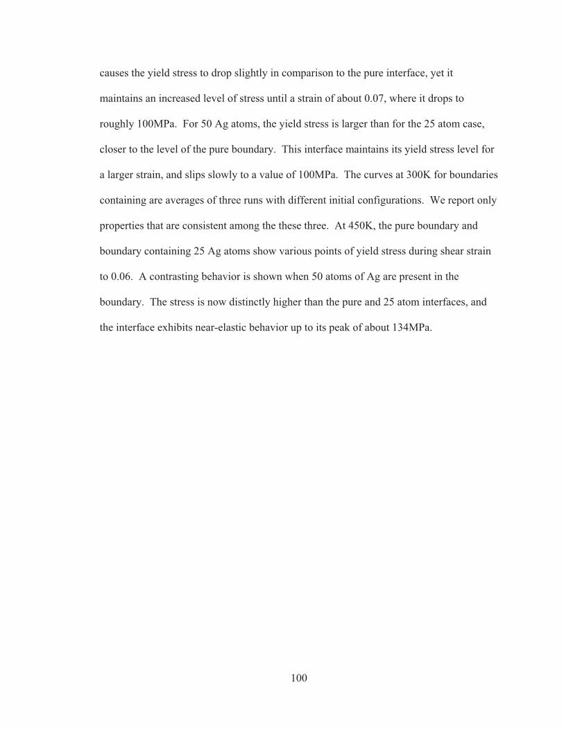
100
causes the yield stress to drop slightly in comparison to the pure interface, yet it
maintains an increased level of stress until a strain of about 0.07, where it drops to
roughly 100MPa. For 50 Ag atoms, the yield stress is larger than for the 25 atom case,
closer to the level of the pure boundary. This interface maintains its yield stress level for
a larger strain, and slips slowly to a value of 100MPa. The curves at 300K for boundaries
containing are averages of three runs with different initial configurations. We report only
properties that are consistent among the these three. At 450K, the pure boundary and
boundary containing 25 Ag atoms show various points of yield stress during shear strain
to 0.06. A contrasting behavior is shown when 50 atoms of Ag are present in the
boundary. The stress is now distinctly higher than the pure and 25 atom interfaces, and
the interface exhibits near-elastic behavior up to its peak of about 134MPa.

101
Figure 5-5 Shear stress (�xz) vs. average strain (�avg) for three solute amounts of Ag at 300K and 450K. Number in squares are solute atom amounts. Curves at 300K are the average of three independent simulation runs. Note different scales for 300K and 450K.
Many of the trends of Ag solute addition are present in the stress vs. strain plots of the
boundary with Cu solute. In figure 5-6 we plot the same shear stress vs. strain behavior
of the pure boundary as was shown in figure 5-5. In the case of Cu at 300K, addition of
25 atoms at the interface causes the yield stress to drop, similar to Ag. We then see a
large decrease at a strain of about 0.07. The stress state for 50 atoms of Cu is elevated
until a strain of about 0.07, where it decreases to a level comparable to the other interface
concentrations. At larger strain in figure 5-6 it appears the interfaces containing solute
are again increasing their level of shear stress as the strain increases. At 450K, the trends
in stress vs. strain are comparable to the Ag solute case. We mention that while 50 atoms

102
of Cu also appears to increases the stress during shear strain, the level is significantly
lower than the 50 Ag atom case from figure 5-6. There are also some small “shoulders”
present in the increasing shear stress portion of the curve, possibly indicating various
degrees of atomic rearrangement.
Figure 5-6 Shear stress (�xz) vs. average strain (�avg) for three solute amounts of Cu at 300K and 450K. Number in squares are solute atom amounts. Curves at 300K are the average of three independent simulation runs. Note different scales for 300K and 450K.
For both types of solute at 300K, the yield stress during boundary shear is lowered upon
the addition of 25 solute atoms. However, a high level of stress is maintained for larger
strains, compared to the pure boundary. After initial slip, shown as a rapid decrease in
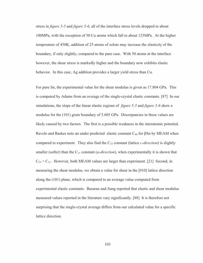
103
stress in figure 5-5 and figure 5-6, all of the interface stress levels dropped to about
100MPa, with the exception of 50 Cu atoms which fall to about 125MPa. At the higher
temperature of 450K, addition of 25 atoms of solute may increase the elasticity of the
boundary, if only slightly, compared to the pure case. With 50 atoms at the interface
however, the shear stress is markedly higher and the boundary now exhibits elastic
behavior. In this case, Ag addition provides a larger yield stress than Cu.
For pure Sn, the experimental value for the shear modulus is given as 17.804 GPa. This
is computed by Adams from an average of the single-crystal elastic constants. [87] In our
simulations, the slope of the linear elastic regions of figure 5-5 and figure 5-6 show a
modulus for the (101) grain boundary of 5.605 GPa. Discrepancies in these values are
likely caused by two factors. The first is a possible weakness in the interatomic potential.
Ravelo and Baskes note an under predicted elastic constant C44 for �Sn by MEAM when
compared to experiment. They also find the C33 constant (lattice c-direction) is slightly
smaller (softer) than the C11 constant (a-direction), when experimentally it is shown that
C33 > C11. However, both MEAM values are larger than experiment. [21] Second, in
measuring the shear modulus, we obtain a value for shear in the [010] lattice direction
along the (101) plane, which is compared to an average value computed from
experimental elastic constants. Basaran and Jiang reported that elastic and shear modulus
measured values reported in the literature vary significantly. [88] It is therefore not
surprising that the single-crystal average differs from our calculated value for a specific
lattice direction.

104
5.2.7 Boundary Sliding in Solute Segregated Boundaries
Simulation work by Qi, et al. investigates the effects of applied force on the sliding of
several grain boundaries. [89] For molecular dynamics simulations of aluminum at
750K, they calculate the critical level of shear stress necessary for sliding to occur, by
varying the magnitude of shear force used. The authors show that for boundaries with
higher excess energy, they observe a lower critical stress value, and an increase in grain
boundary sliding. Namilae, et al. compute static energies of Al grain boundaries and
corresponding amount of slip when under shear. [83] Similarly, they show for higher
energy boundaries, the sliding amount is greater. Previous work by the current authors
quantified the energy of the (101) �Sn grain boundary and various others using
molecular simulation. [80] The (101) boundary had the highest energy (and highest self-
diffusivity) relative to the other boundaries investigated, and from comparison to other
work, we can say that the pure (101) boundary will most likely exhibit the largest amount
of sliding and lowest yield stress when compared to the other boundaries studied in ref.
[80].
Investigations of sliding resistance by Millett, et al. find a decrease in the excess energy
of the grain boundaries upon solute addition, and a corresponding resistance to sliding.
[90] In Millett, et al.’s 2006 work, the effect of both interstitial and substitutional atoms
were investigated. It was found for low energy (310)-05 boundaries and higher energy
boundaries, interstitial atoms and oversized substitutional atoms hindered sliding, while
undersized substitutional atoms increased sliding for the higher energy boundary. From
this, they note a correlation between enthalpy of segregation of the solute species and
sliding resistance. Solute that is strongly segregating will aid in sliding resistance.

105
Results of our Ag and Cu additions into the (101) boundary follow this to some extent.
Initially, the yield stress is lower for the interfaces containing 25 atoms of solute
compared to the pure boundary, so these boundaries will begin sliding at a lower critical
stress (in the context of Qi, et al. [89]). After leaving the elastic regime however, a high
stress is maintained for those interfaces containing 25 and 50 solute atoms. This
indicates a higher resistance to sliding at larger strains in comparison to the pure
boundary.
5.2.8 Interface Structure During High Temperature Sliding
Taking a closer look at their sliding displacement vs. time plots, Qi et al. discuss a change
from a linear to parabolic slope as the force changes. [89] The authors attribute this
change to an increase in atomic disordering at the interface, where a parabolic slope is
created by a large shear force perturbing the boundary region and increasing the atomic
mobility. As the applied shear force increases, the mobility of the atoms at the interface
increases.
Our pure boundary undergoes a similar transition at 450K, as time progresses during our
constant shear velocity simulation. Initially, the interface becomes disordered over a 10-
15 Å width that is perpendicular to the interface. This is followed by coexisting regions
of ordered planes of atoms and mobile pocket of disordered atoms, maintained until a
strain of about 0.04. At this point, there is a transition into a structure that envelopes the
entire interface plane. The new phase in the interface, which is five atomic layers thick,
slides relative to the �Sn lattice on planes above and below it, as shear progresses. This
final structure is illustrated in figure 5-7. Here, the blue and red colored planes are those
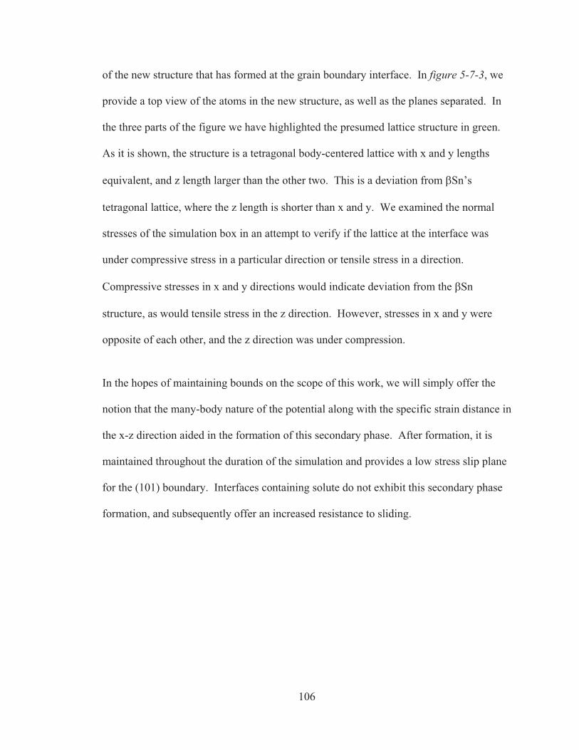
106
of the new structure that has formed at the grain boundary interface. In figure 5-7-3, we
provide a top view of the atoms in the new structure, as well as the planes separated. In
the three parts of the figure we have highlighted the presumed lattice structure in green.
As it is shown, the structure is a tetragonal body-centered lattice with x and y lengths
equivalent, and z length larger than the other two. This is a deviation from �Sn’s
tetragonal lattice, where the z length is shorter than x and y. We examined the normal
stresses of the simulation box in an attempt to verify if the lattice at the interface was
under compressive stress in a particular direction or tensile stress in a direction.
Compressive stresses in x and y directions would indicate deviation from the �Sn
structure, as would tensile stress in the z direction. However, stresses in x and y were
opposite of each other, and the z direction was under compression.
In the hopes of maintaining bounds on the scope of this work, we will simply offer the
notion that the many-body nature of the potential along with the specific strain distance in
the x-z direction aided in the formation of this secondary phase. After formation, it is
maintained throughout the duration of the simulation and provides a low stress slip plane
for the (101) boundary. Interfaces containing solute do not exhibit this secondary phase
formation, and subsequently offer an increased resistance to sliding.

107
Figure 5-7 Structural formation in pure GB interface at 450K under shear. (1) Side view in y-z plane. (2) Side view in x-z plane, shear direction indicated. (3) Top view of full BCC structure and separate lattice planes.
5.3 Conclusions
We investigated the excess enthalpy of the �Sn (101) grain boundary containing various
amounts of Ag and Cu solute atoms. as well as its behavior under shear strain. It is
shown that an increase in either type of solute at the interface lowers the excess enthalpy
of the grain boundary. We then find the enthalpies of segregation for both solute types,
computed as the slope of excess enthalpy of the grain boundary per area vs. interfacial
solute concentration per area. Under constant shear strain, addition of solute lowers the

108
yield stress of the boundary, but for larger strain, stress levels are maintained when
compared to the pure case.
For Ag solute, we find it has a greater driving force for segregation and thus lowers the
excess energy of the boundary more than Cu for a given number of atoms for the (101)
boundary. Experimental works from other authors discuss the change in microstructure
for different amounts of solute in Sn-xAg and Sn-xCu solder joints in the context of Ag
addition aiding in destabilizing special boundaries, and high concentration Cu addition
forming Sn-Cu IMC and pinning �Sn grains. In regards to Ag, we observe only a
reduction in excess grain boundary enthalpy, showing the beginnings of (101) interface
stabilization. A short investigation of the (301) and two medium energy boundaries
found very low, but positive, segregation enthalpies for Ag and Cu in the special
boundary, and experimentally comparable segregation enthalpies for the (310) and (201)
boundaries. However, considering the statistical uncertainty in the (301) results, these
values indicate that an increase in that particular boundary excess energy is possible. We
do find one experimental case where a 03 boundary’s energy increased upon Mg
addition, however numerous experimental works show solute atoms stabilizing grain
boundaries, both low and high energy, as indicated by the solute’s positive enthalpies of
segregation (in our context). To completely rule out the possibility of “destabilization”
by Ag solute however, more specific investigations should be carried out.
Cu and Ag solute both affected the behavior of the (101) boundary under constant shear
strain. At 300K, the pure boundary exhibited the highest yield stress. Interfaces with
either Ag or Cu however, maintained a high level of stress after yield, followed by a

109
quick decrease in stress to a value similar to that of the pure boundary. High temperature
shear brought about almost no stress response from the pure boundary, and the initially
disordered interface underwent a structural transition into a tetragonal body centered
structure at long simulation time. With solute addition however, the boundary disordered
less and showed no structural transitions. Large solute concentrations evoked elastic
behavior from the boundary under shear, and yield stress values were about 50% and
25% of the 300K case, for Ag and Cu respectively. Overall, Ag and Cu solute addition at
low and high temperature restricts �Sn (101) grain boundary sliding, evidenced by
elevated values of stress at larger strains.

110
Continuing the investigation of transport in microcrystalline and polycrystalline �Sn, in
this chapter we measure the self-diffusivity of Sn in a (101) symmetric tilt �Sn grain
boundary containing various amounts of Ag and Cu solute. Using the Modified
Embedded-atom method as an interatomic potential, we are able to quantify the effect
that Ag and Cu have on the grain boundary self-diffusivity of Sn at typical solder
operating temperatures. Additionally, we determine the effect solute has on the diffusive
width of the grain boundary and offer insight into the unique characteristics of the grain
boundary resulting from the two types of solute.
Solute Effects on Grain Boundary Self-Diffusivity
“And it must follow, as the night the day...”

111
Underscoring the importance of determining, not only transport properties of the joint
solvent material, but also the effects of dopants or solute additions on transport, is the
experimental work by Bernardini, Gas, et al. [91] In their 1982 work, they observe a
decrease in the self-diffusivity of Fe as Sn solute atoms strongly segregate to the grain
boundary. Molecular simulation is well suited to complement this type of study.
Preliminary work using simple model systems has shown the effects of substitutional
dopant atoms on Cu grain boundaries and in Cu polycrystals. [48] Although these studies
approximate quantities such as excess entropy through the use of McLean’s model and
extensions, atomistic detail of concentrations and transport for particular structures can be
measured. [44][80]
This chapter continues with specifics of our molecular simulations in Section 6.1. We
then present and discuss our findings in Section 6.2, and end with concluding remarks in
Section 6.3.
6.1 Simulation Details
In our simulations, and similar to Chapter 5, we model the (101) symmetric tilt grain
boundary of �Sn, with varying amounts of solute particles randomly placed in interstitial
positions along the interface. The grain boundaries and randomly inserted solute
configurations are again constructed with the Etomica Molecular Simulation API, and for
solute species we use Ag and Cu. [76] Interactions between Sn and Ag, and Sn and Cu
are modeled with MEAM in the LAMMPS Molecular Simulator. [58][70] We follow the
same system setup as in Chapters 4 and 5, and a similar equilibration setup which we
explain in the following.

112
Table 6-1 Ag and Cu solute quantities and corresponding excess interfacial density.
Ns (atoms) 5 10 25 50
�s (10-3 atoms/Å2) 2.085 4.171 10.43 20.85
The process of minimization of the grain boundary is done in three steps. First, near 0K
the two grains move independently in x, y, and z-directions via molecular dynamics, their
respective atoms all having the same average force each time step. This step is shown in
(figure 6-1-1). Next, solute atoms are randomly inserted at interstitial positions in the
grain boundary interface. Shown in table 2 are the specific amounts of solute inserted
and their corresponding interfacial excess density. The positions of the solute atoms are
then adjusted via a conjugate gradient energy minimization, while holding the Sn atoms
fixed (figure 6-1-2).
Figure 6-1 (1) minimization (MD near 0K), (2) solute minimization (conjugate gradient), (3) equilibration, (4) production structures. Black arrows indicate direction of motion of the block portion. Free atoms are movable in x, y, and z directions. Actual simulation cells are 3-dimensional and periodic in x and y directions.
Finally, once a minimum energy structure is found, the system is then equilibrated using
molecular dynamics (MD) at the desired production run temperature (figure 6-1-3).

113
Here, atoms in the bottom grain within twice the potential cutoff distance of the bottom
edge of the structure are fixed and atoms in the top grain within twice the potential cutoff
distance of the top edge of the structure are given an average force in the x, y, and z-
directions. This creates a floating boundary at the top of the box and allows the system to
reach an average pressure of zero over 100 picoseconds. Following these steps, the
floating boundary is fixed and the grain boundaries are simulated with MD between 9 and
15 nanoseconds (figure 6-1-4). All molecular dynamics is carried out with a Nose-
Hoover thermostat (NVT) and a time-step of 0.001 picoseconds.
6.2 Results and Discussion
Using MD over a range of temperatures, we simulate the (101) symmetric tilt grain
boundary of �Sn. At each temperature, specific quantities of solute atoms of Ag and Cu
are randomly inserted at the grain boundary interface and the width-scaled Sn self-
diffusivity is calculated. We also analyze the planar self-diffusivity profiles in the
direction perpendicular to the grain boundary interface. From this we can quantify the
interface's diffusive width �GB and characterize the effect that Ag and Cu have on the
interface structure of �Sn.
6.2.1 Grain Boundary Width-Scaled Diffusivity (�GBDGB ) of Sn
We compute the mean-squared displacement of Sn for multiple MD runs at a given
temperature and specific solute concentration. By employing equation (2-24) from
Section 2.2.3, we plot the width-scaled diffusivity vs. temperature in figure 6-2 for each
type of solute over a range of quantities and temperatures. For Ag and at low

114
temperatures, the diffusivity of Sn does not exhibit any type of clear trend with increasing
solute concentration. Statistically, the points at 300K and 350K are very close in
magnitude. However, as the temperature increases, we see the Sn diffusivities for
specific solute amounts begin to deviate. At 450K, the diffusivity for a system with 50
solute atoms is decreased by an order of magnitude when compared to the 5 solute atom
system and by about one-third when compared to the 25 solute atom system. With the
addition of Cu instead of Ag, the trends are similar but less pronounced. We see a
smaller deviation in the diffusivity of Sn at higher temperatures with respect to solute
concentration—about twice the diffusivity at 5 atoms than at 50 atoms. In contrasting the
two solute types, the addition of 25 and 50 atoms of Ag lowers the diffusivity of Sn more
than similar quantities of Cu. For small numbers of solute, the effect of Ag and Cu are
statistically similar on this width-scaled diffusivity plot.

115
Figure 6-2 Width-scaled self-diffusivity of Sn vs. temperature for various solute atom quantities. LEFT is Ag solute, RIGHT is Cu solute. Error bars are standard deviation from three or more simulation runs.
6.2.2 Planar Self-Diffusivity Profiles and Interface Width
For a closer look at the diffusive properties of Sn and an opportunity to investigate its
interface structure, we plot the planar self-diffusivity in planes parallel to the grain
boundary interface. For clarity in the plots in figure 6-3 and figure 6-4, only profiles
from a single run are plotted, however, the single run chosen was the one with a
diffusivity closest to the average. Also, note the change in scale on the plots’ y-axes.
The profiles for varying Ag amounts at temperatures of 300K, 350K, 400K, and 450K are

116
shown in figure 6-3. Similar to figure 6-2, at temperatures of 300K and 350K the authors
are unable to discern any trend in diffusivity when increasing solute amount. Although at
300K, the profiles show a decrease in diffusivity when increase solute amount from 5
atoms to 10, and from 5 atoms to 50, the same does not hold true for profiles at 350K. At
400K and 450K, the effect of solute on Sn self-diffusivity is clearly evident and is
amplified as temperature increases. Widths of the profiles remain relatively stable as
temperature increases and as solute increases.
A similar analysis is completed for Cu solute in the �Sn grain boundary and illustrated in
figure 6-4. Again, the scales of the plots y-axes vary with temperature, but are equivalent
to those in figure 6-3 at specific temperatures for the sake of comparison. In figure 6-4,
the effect of Cu solute on the self-diffusivity of Sn with increasing solute amount occurs
at 350K and continues to high temperature. The effect of specific solute concentrations
on diffusivity becomes more distinct as temperature increases. As solute concentration is
increased, we see in an increase in diffusive width at all temperatures, with the increase at
450K being the least prominent. Additionally and perhaps most importantly, the
interface diffusivity profiles exhibit a change from a single peak at 5 and 10 atoms of Cu
to double peaks at 25 and 50 atoms of Cu.
Further evidenced by the planar diffusivity profiles in figure 6-3 and figure 6-4 is the
effect of solute on Sn self diffusivity. Both Ag and Cu decrease the planar diffusivity in
the (101) grain boundary at temperatures at 400K and above, although the effect of Cu is
seen at 350K. It is shown here however, that Ag plays a larger role. At 350K and 400K,
peaks in the diffusivity of the Ag system are significantly lower than systems with Cu, for

117
corresponding temperatures. In the comparison of �Sn's structure for different solute
types, we see no qualitative difference in interface width with temperature for Ag as
solute, but for Cu, it is apparent that the interface width grows with increased solute
amount and the diffusive profile changes shape at large solute amounts. The center of the
�Sn grain boundary interface containing Cu exhibits slower diffusion than at the edges of
the interface containing no Cu. To further characterize this behavior we quantify the
interface width at a range of temperatures for various solute concentrations, as well as
inspect simulation snapshots and trajectories.
Figure 6-3 Planar self-diffusivity profiles in z-direction of Sn for various solute atom quantities of Ag at a particular temperature. Note different scales on each ordinate.

118
Figure 6-4 Self-planar diffusivity profiles in z-direction of Sn for various solute atom quantities of Cu at a particular temperature. Note different scales on each ordinate.
An analysis of the full-width at half maximum of the planar self-diffusivity profiles in
figure 6-3 and figure 6-4 is shown in figure 6-5. Here, we quantify the diffusive width of
the (101) grain boundary interface with varying solute amount at a range of temperatures.
It is important to mention that the analysis assumes a profile that is Gaussian-like, yet
width computation from our profiles of the �Sn interface with large amounts of Cu solute
deviate from this. In our analysis of these profiles, the maximum is taken as the highest
peak of the two. This introduces the possibility to skew or induce spurious width
determinations for very high peak and very low "trough" regions. However, the profiles
in our case exhibit only moderate dips in diffusivity over the range of x-y planes, and it is
unlikely that this affects the width measurements in such a manner.
At figure 6-5 - LEFT, it is shown that diffusive widths for the (101) interface containing
Ag increase very little with solute concentration and temperature. In comparison to a

119
pure �Sn interface (shown as black circles), the width has decreased by at most 1Å with
the addition of Ag solute. As Cu is inserted at the interface (figure 6-5 - RIGHT), an
increase in interface width with temperature is more obvious, as is the increase in width
with solute amount. At 25 and 50 Cu atoms in the interface, the width of the (101) grain
boundary exceeds the pure boundary width for temperatures above 300K. There is also a
marked difference in widths between Ag and Cu at solute amounts of 50 atoms. The
amount of Ag solute seems to have no effect on the width, while the addition of Cu
causes a distinct increase in width.
Figure 6-5 Diffusive width vs. temperature for various solute concentrations. LEFT is Ag and RIGHT is Cu. Circle points (black) are the pure �Sn grain boundary widths.

120
We have shown thus far that the addition of both Cu and Ag decrease Sn self-diffusivity
in the (101) �Sn grain boundary. Separately, Ag reduces the diffusivity more than Cu
and promotes a smaller diffusive width of the grain boundary. With Cu addition, small
amounts of solute give the same effect on diffusivity as Ag addition, but as the Cu
amount is increased to 25 and 50, the grain boundary width grows larger than that of pure
�Sn. Evidence of this is shown in the planar diffusivity profiles for �Sn with Cu added.
At values of 25 and 50 atoms of Cu, we see wide profiles with two peaks in diffusivity,
indicating a slower diffusing plane of the interface, sandwiched by two fast diffusing
planes. We attempt to describe this behavior through the visual analysis of rendered
simulation trajectories of both Ag in �Sn and Cu in �Sn. In figure 6-6 we show a
rendered snapshot of Ag in the (101) grain boundary (LEFT) and Cu in the boundary
(RIGHT). These shots are taken from a simulation run at 450K, both containing 50 atoms
of respective solute. It is evident that the amount of disorder in the system containing Ag
is less than in the system containing Cu. This observation can explain the difference in
diffusive widths of the two systems. A more ordered interface will be less mobile and
exhibit a lower value of diffusivity.

121
Figure 6-6 Rendered simulation snapshot of two grain boundaries at 450K and containing 50 solute atoms in the interface. LEFT is Ag (green) and RIGHT is Cu (orange).
6.2.3 Effect of Atomic Size and Cohesive Energy
With a focus on the system with Cu added, the full trajectory (of which figure 6-6 is a
snapshot) shows that the Cu atoms maintain their z-axis position at the center x-y plane
of the interface. This plane corresponds to the "troughs" seen in figure 6-4 profiles at
higher solute concentration. Yet, only part of the interface behavior is described by Cu's
z-axis position, and still unexplained are the highly mobile regions of �Sn in planes
above and below the Cu solute. For this, further analysis of the trajectory was necessary.
In observing the Cu solute atom's subtle motion in the central z-plane of the interface, we
notice a preferred coordination of Sn around the Cu atom. Motion of the Cu atom is
actually a concerted motion of a Cu and 4-Sn cluster.

122
A coordination similar to that of Cu is not seen for the other solute, Ag. This preference
is described in a fairly straightforward manner by comparing the cohesive energies used
in the MEAM potential, listed in table 2-1. We remind the reader, as mentioned in
Chapter 5, Sn-Sn interactions carry a cohesive energy of 3.08eV, Ag-Sn is lower at
2.83eV, and Cu-Sn is higher at 3.5eV. At the interface, Sn-Sn interactions are preferred
over Ag-Sn, while Cu-Sn interactions are favored over Sn-Sn. The larger cohesive
energy of the Cu-Sn system is shown in the simulation trajectories to induce local
ordering in the interface, which at larger distances creates disordering when in contact
with the �Sn lattice. For an interstitial Cu in the bulk �Sn lattice, the quality of the
surrounding �Sn structure may keep the preference for Cu-Sn ordering at bay.
Conversely, when Cu is present at the grain boundary, the already low-coordinated Sn
atoms are free to rearrange and form clusters with Cu. It appears these clusters are not
structurally compatible with the �Sn lattice and create more disorder at the grain
boundary. As such, the cohesive energy of Cu-Sn interactions actually increases
diffusivity with respect to a Ag solute through the secondary effect of structural
disruption at the interface.
Further comparison of the MEAM properties of Ag, Cu, and Sn, reveal that equilibrium
values of the reference structure lattice constants r0 vary as well. For analysis in this
work, values of r0 can be thought of as corresponding to relative atomic size—here Cu is
smaller than Ag, and both are smaller than Sn. Because there is variation in both
cohesive energy and size of the solutes, we cannot say definitively what effect the larger
size of Ag has on the decreased mobility of Sn in the (101) interface. Nevertheless, other
works have investigated the separate effects of atomic size and cohesive energy

123
mismatch. We again highlight the work by Millet, et al., referenced in Chapter 5, on the
role dopant atoms play in grain boundary energetics and overall stability of nanocrystals.
[46] In a 2005 investigation, they examined the effect of Lennard-Jones dopant
particles—over a range of sizes and cohesive energies (� and 8)—on grain boundary
energy. They demonstrated that while the overall contribution of a dopant atom's
cohesive energy does not play a significant role in decreasing the energy of the solvent
grain boundary, the size of the dopant atom as compared to the host atom is influential in
affecting the energy. This is explained by a reduction of tensile stress at the grain
boundary through the insertion of a dopant atom. Furthermore, for sizes of the dopant
ranging from smaller than the host atom to larger than the host atom, the larger the
dopant, the greater the decrease in grain boundary energy. In our case, one can equate a
grain boundary energy with a grain boundary diffusivity by referring to both empirical
relationships and trends observed in simulation. [30][80][92] Accordingly, we can say
that the size of Ag plays an important role in the reduction of the self-diffusivity of Sn, as
a result of a reduction in grain boundary energy.
A final comparison of the two solutes at high concentration is made in figure 6-7, where
for 50 atoms of corresponding solute, we show planar diffusivity profiles at a range of
temperatures. Noting the different scales on the plots’ y-axes, it is shown that at
temperatures of 400K and 450K, diffusivity is exceptionally hindered by Ag when
compared to Cu. Again we see evidence of Ag’s greater reduction in Sn self-diffusivity
at the grain boundary versus Cu, here at similar concentrations. Still, whether this an
effect of atomic size or decreased cohesive energy, we cannot state conclusively.

124
Figure 6-7 Self-planar diffusivity profiles of �Sn in z-direction for solute atom quantities of 50 at various temperatures. LEFT is Ag and RIGHT is Cu. Note different scales on ordinate.
6.2.4 Grain Boundary Self-Diffusivity (DGB) of Sn
After the direct calculation of grain boundary widths from plots in figure 6-3 and figure
6-4, we can resolve the true grain boundary self-diffusivity of Sn, namely DGB in units of
length2/time. In doing so we have removed the effect of the interface width on the
magnitude of the diffusivity. Specifically, we have normalized the quantity �GBDGB at
various temperatures and solute amounts by the corresponding grain boundary width �GB
at the same conditions. This is shown in figure 6-8. In comparison to figure 6-2, low

125
temperature values of DGB for the system with Ag added show very little change relative
to �GBDGB, and at higher temperatures the relative magnitudes of DGB are separated by a
slightly larger amount. For Cu, low temperature diffusivities have collapsed to a smaller
range of values for varying solute concentration. At temperatures of 400K and 450K,
solute amounts of 25 and 50 show a greater deviation from amounts of 5 and 10.
Removing any variation of grain boundary width with temperature or solute
concentration, allows us now to speak definitively about possible changes in diffusion
rates or mechanisms of Sn. While there is a reduction in the magnitude of diffusivity
with increased solute concentration, there is not a clear change in slope in these
Arrhenius style plots. Therefore, we can say that the addition of Ag and Cu in low
amounts influences the number of diffusive events, but does not affect the mechanisms of
diffusion. For a mobile boundary like the (101) in �Sn, this is not surprising, and the
interface may require larger solute concentrations or precipitation effects for it to exhibit
a change in mechanism style.

126
Figure 6-8 Self-diffusivity of Sn vs. temperature for various solute atom quantities. LEFT is Ag solute, RIGHT is Cu solute.
6.3 Conclusions
This work investigated the effect of solute atoms of Ag and Cu on the self-diffusivity of
Sn in the (101) symmetric tilt �Sn grain boundary. Through molecular dynamics
simulations of various solute amounts, and over a temperature range of 300K to 450K,
we show that both Ag and Cu decrease the grain boundary self-diffusivity of Sn as solute

127
amount in the interface increases. The magnitude of these reductions and secondary
effects from each solute were also explored.
From the primary quantity of self-diffusion measurement in grain boundaries, �GBDGB,
the effect of solute was shown in an Arrhenius style plot. For increasing solute amounts,
the width-scaled diffusivity decreased at temperatures above 350K. There was also a
greater decrease in this value for the Ag solute when compared to the Cu solute.
Magnitudes at temperatures of 300K and 350K for both solute types were inconclusive
regarding the effect of solute amount.
To quantify the width of the (101) grain boundary interface, planar diffusion profiles
were plotted at various solute amounts and temperatures. For Ag, we saw again that an
increase in the solute amount leads to a decrease in the self-diffusivity of Sn and over the
range of temperatures the relative shape and width of the profiles remains constant.
Profiles of Cu exhibit similar behavior in reducing the diffusivity in the interface, albeit
by a smaller amount. In contrast to Ag, diffusion profiles for large amounts of Cu
develop a double peak structure, with a slower diffusive “trough” at the center plane of
the interface and an increased diffusive width. After visual analysis of simulation
trajectories, we state that the cohesive energy of the Cu-Sn interactions creates highly
coordinated clusters of Sn around single Cu atoms. This essentially induces a local order
at the center of the interface and structural disorder the longer distances.
The diffusive widths of the planar profiles are also quantified using a full-width at half
maximum analysis. From this we see no increase in the width of the (101) boundary upon

128
addition of Ag or increase in temperature—in fact the width is less than that of the pure
(101) boundary. However, with the addition of Cu to the (101) grain boundary interface,
there is an increase in width, and at solute amounts of 25 and 50 atoms, the width
surpasses that of the pure (101) boundary. Also, with 50 Cu atoms in the interface, the
diffusive width increases significantly with temperature to a value almost twice that of
the pure interface. This is the effect of the large cohesive energy of Cu-Sn presenting
itself.
Finally, using the calculated diffusive widths �GB at each temperature and solute amount,
we normalized the measured �GBDGB quantity to resolve a grain boundary diffusivity
independent of width. This also allows us to comment on possible shifts in diffusion
mechanisms at the interface. An Arrhenius plot of DGB vs. T exhibited similar trends in
the magnitude of diffusivity for each solute type and amount, as compared to the plot of
�GBDGB vs. T. It is also evident that the slope of the diffusivity at a specific solute amount
does not change significantly, indicating a common diffusion mechanism throughout the
range of solute amounts studied.

129
There is a vast opportunity for molecular simulation to aid in the modeling of damage
phenomena occurring in the electronics packaging of today’s high power devices and
tomorrow’s nanoelectronics. Lead-free solder joints in particular, when under large
current densities and temperature gradients, exhibit significant mass transport governed
by the atomistic microstructure of the joint. Vacancies flow quickly through the joint’s
�Sn grain boundaries leading to excess stress buildup, cracking, and eventual failure.
Molecular simulation examines this problem at the atomic level and lends quantitative
material properties of transport and structural behavior to micro- and macro-scale models
as a way to better characterize the damage in the joint. The investigations in this
dissertation are presented as contributions to larger scale damage models, and through the
Conclusions and Future Work
“This is too long.”

130
study of �Sn surfaces, grain boundaries, and solute effects, we offer properties relating
to diffusivity, boundary energy and stability, as well as justifications of experimentally
observed behavior.
Chapter 3 investigates the energy and diffusivity of �Sn surfaces corresponding to low
Miller index planes. The (100) surface is identified as exhibiting the lowest excess
potential energy, and various diffusion mechanisms of an adatom moving on that surface
are determined. These properties are valuable in describing void morphology and
stability under electromigration in metals. We continue the study of �Sn structure with
several molecular dynamics simulations of grain boundaries. The excess potential
energy, grain boundary diffusivity, and interface width are determined for five grain
boundaries in Chapter 4. The diffusivity results are in good agreement with experimental
diffusion studies of polycrystalline Sn, however we find that the widths of a few of our
boundaries are larger than the estimated value used in experiment. An interesting case is
also presented, describing a boundary that exhibits fast channel like diffusion, but has a
low excess energy. In these two chapters, simulations of pure Sn structures confirm
experimental work and complement it by offering quantitative values of transport
properties on surfaces and in grain boundaries, and additional parameters such as excess
energies and diffusive widths.
Chapters 5 and 6 consider the effects of Ag and Cu solute addition on the �Sn (101) grain
boundary. In Chapter 5, the excess energies of the (101) interface containing various
amounts of solute are quantified, and the segregation enthalpy is determined for both Ag
and Cu. Ag is shown to have a larger positive value compared to Cu, but by definition,

131
both lower the energy of the (101) boundary upon segregation from the bulk. Much
experimental and simulation work is presented that validates this behavior. One
simulation case finds the opposite, however; that Mg increases the energy of a particular
Al grain boundary. Additionally, experimental work characterizing the microstructure in
solder joins with different concentrations of Sn-xAg and Sn-xCu concludes that Ag
increases the energy of special boundaries, to inhibit grain growth, and creating a finer
microstructure full of many grain boundary types. Similarly, they state that Cu decreases
the energy of special boundaries, allowing them to consume higher energy boundaries,
leading to a coarser microstructure. We investigate this claim by simulating the (301)
boundary, a low energy, special boundary identified in the experimental work, as well as
two other medium energy boundaries. We find that Ag and Cu lower the energy of this
particular boundary only slightly, much less than their effect on the (101) boundary.
With respect to the computed enthalpies of segregation, statistically it is possible that Ag
could increase the energy of this boundary, as its value is close to zero, albeit only
slightly. The two medium energy boundaries exhibit enthalpies of segregation for both
Ag and Cu that are experimentally comparable in magnitude to several reported studies.
We conclude that there is a much larger driving force for Ag to stabilize higher energy
boundaries, rather than increase the energy of special boundaries, and this is most likely
the behavior leading to the fine microstructure present in Sn-xAg solder joints. For Cu,
since it stabilizes the boundaries less, a fine microstructure does not develop in Sn-xCu
joints until very high concentrations of Cu are present and an intermetallic phase is
formed, pinning the �Sn grains. This type of structure is observed in other experimental
studies.

132
The effects of solute addition on shear stress are also probed in Chapter 5. It is shown
that while addition of Ag and Cu to the (101) boundary slightly lower the yield stress,
this value is maintained during further shear. This indicates an increased resistance to
boundary sliding. We also quantified the shear modulus of the (101) boundary and find
that it is about 30% smaller than the experimental average value for single crystal Sn, and
remains unchanged with solute addition. This discrepancy may be due to an under
prediction of an elastic constant by the MEAM potential and the fact that we compute the
shear modulus for a specific lattice direction.
In our final chapter, the study on solute effects is continued, and we determine to what
extent the self-diffusivity of the �Sn (101) grain boundary is changed upon solute
segregation. It is found by examination of planar diffusivity profiles that both solutes
decrease the self-diffusivity, but Ag addition lowers the diffusivity of Sn to a greater
extent than Cu. Also, we find for higher values of Cu, the interface disorders and the
diffusive width increases to a value twice that of the pure boundary. A closer look at
simulation snapshots reveal highly coordinated Cu-Sn structures, illustrating a short
range order, with a longer range disorder. We explain this by comparing the cohesive
energies of Ag-Sn, Sn-Sn, and Cu-Sn. Cu-Sn is the largest, and in the presence of a
disordered boundary, Cu can freely coordinate with Sn in a favorable structure, thereby
increasing the diffusive width of the boundary.
Taken in concert, these chapters present a microstructural picture of the lead-free solder
joint. We have identified surfaces and interfaces of �Sn, likely present in the many
structural regimes of the joint, and reported their various transport properties. Increasing

133
the scope of the study, we report the atomistic effects of Ag and Cu solute addition on the
(101) and (301) grain boundaries, examine their separate effects on boundary energy,
diffusivity, and resistance to shear stress, and provide explanations for experimentally
observed grain structure.
7.1 Original Contributions
This dissertation presents several new and significant additions to the field of lead-free
electronics packaging research. Although determined computationally, many of these are
quantitative material properties that show very good agreement with experimental data.
For this reason, the validity of our models is strong, and the interesting atomic scale
behavior that is investigated in this work is used to explain existing experimental
observations. The various contributions are singled out here.
; In Section 2.4, we use the volumetric strain in an Al lattice to develop a consistent
relationship describing the relative size of a lattice vacancy via a vacancy relaxation
factor. Before this work, the vacancy relaxation factor was reported in various
ways, often with dimensional inconsistencies.
; The lowest energy �Sn surface for low index Miller planes is computed in Chapter
3, and the anisotropic tracer diffusivity is determined. This surface is shown to be
present in experimental thin-film growth. At the time of publication, it is the belief
that this is the first calculation of the diffusivity of a Sn surface.
; Chapter 4 details the quantification of specific grain boundary diffusivities for �Sn
interfaces. These show good agreement with experimental work on polycrystals.

134
Previously uncalculated grain boundary widths and energies are reported, and a
low-energy grain boundary is characterized as exhibiting fast channel diffusion.
; Through Ag and Cu solute addition studies in Chapter 5, we demonstrate that the
energy of the (101), (201), and (310) grain boundaries can be reduced. This is in
agreement with general theory and other general simulation work. Critical values
of interfacial concentration are calculated, and it is determined that reducing the
boundary energy to zero would require an extreme amount of interfacial solute.
; Additionally, we compute the shear modulus in [010] for the (101) grain boundary,
and illustrate the boundary’s behavior under shear, in the presence of solute. Ag
and Cu are shown to improve the resistance of the boundary to slipping, in
agreement with general simulation work.
; In Chapter 6, it is shown that Ag and Cu addition can dramatically reduce the self-
diffusivity of �Sn in the grain boundary interface. Ag invokes a greater reduction
because of its larger covalent radius and weaker cohesive energy, with respect to
Cu.
; We also show that Cu’s large cohesive energy causes local structural ordering and
long-range disordering in the grain boundary. This increases the diffusive width of
boundary compared to Ag addition, and at large Cu concentration, the boundary
develops a bimodal planar diffusion distribution.
7.2 Recommendations of Future Work
With the availability of accurate interatomic potentials for Sn and its alloy interactions,
much work can be done in the study of these compounds with respect to lead-free solder

135
joints. Possibly the chief contribution to the field from a methodology standpoint is the
development of a technique to equilibrate a given amount of solute in and around a grain
boundary in a reasonable amount of simulation time. This was attempted using Monte
Carlo moves of solute-vacancy swaps, and expansion and contraction of local Sn
neighbors. However, developing moves that gave practical Boltzmann factors proved
more complicated that initially thought, and work on this project stopped. This type of
scheme has worked for some other Grand Canonical simulations (an interested reader is
pointed to work by Stephen M. Foiles on Ni-Cu alloys [93]), but the large difference in
the Sn lattice around the neighborhood of an interstitial solute versus a vacancy creates a
roadblock not easily overcome by current methods.
Another recommendation is to expand the Sn system into a larger nano- or polycrystal.
This type of system may be able to connect more easily to finite element level models, if
not work directly in tandem. It also represents a more direct experimentation of solder
microstructure, and effects of solute can be introduced to examine the dynamics of grain
growth and grain sliding. The reader is referred to a kinetic Monte Carlo simulation
package in development at Sandia National Laboratory called SPPARKS.
Finally, in the search for better solder compounds, molecular simulation can play a big
role. With the ability to parameterize the MEAM potential for single and binary
component materials, potentials for new alloying compounds in Sn can be developed.
Characteristics of �Sn, Ag, and Cu should be considered when investigating new
components, and calculations improved by including a measure of entropic contributions
to further quantify solute-solvent interactions in different microstructures.

136
[1] Kirchheim, R., Acta Metallurgica et Materialia 40 (2), 309-323 (1992).
[2] Kirchheim, R., Materials Research Society Symposium Proceedings 309, 101-110 (1993).
[3] Basaran, C., Lin, M., Ye, H., International Journal of Solids and Structures 40 (26), 7315-7327 (2003).
[4] Basaran, C., Lin, M., International Journal of Materials and Structural Integrity 1 (1,2,3), 16-39 (2007).
[5] Li, S. and Basaran, C. Mechanics of Materials, 41 (3), 271-278 (2009).
[6] DIRECTIVE 2002/95/EC OF THE EUROPEAN PARLIAMENT AND OF THE COUNCIL, http://eur-lex.europa.eu/LexUriServ/LexUriServ.do?uri=OJ:L:2003:037:0019:0023:EN:PDF
References

137
[7] NIST Materials and Metallurgy http://www.boulder.nist.gov/div853/lead_free/props01.html
[8] Lloyd, J.R. and K.N. Tu, Handbook of lead-free solder technology for microelectronic assemblies, 827-850 (2004).
[9] Singh, P. and Ohring, M. Journal of Applied Physics 56 (3), 899-907 (1984).
[10] Dyson, B. Journal of Applied Physics 37 (6), 2375-2378 (1966).
[11] Dyson, B., Anthony, T.R., Turnbull, D. Journal of Applied Physics 38, 3408 (1967).
[12] Korhonen, M., Paszkiet, C.A, Li, C. Y., Journal of Applied Physics 69 (12), 8083-8091 (1991).
[13] Sarychev, M.E., Zhitnikov, Y.V., Borucki, L., Liu, C.-L., Makhviladze, T.M., Journal of Applied Physics 86 (6), 3068-3075 (1999).
[14] Sarychev, M.E., Zhitnikov, Y.V., Borucki, L., Liu, C.-L., Makhviladze, T.M., Thin Solid Films 365, 211-218 (2000).
[15] Kirchheim, R. and Kaeber, U. Journal of Applied Physics 70, 172-181 (1991).
[16] Li, S. and Basaran, C. Computational Materials Science 47, 71-78 (2009).
[17] Telang, A.U., Bieler, T.R., et al. Journal of Electronic Materials 33 (12) (2004).
[18] Seo, S-K., Kang, SK., Shih, D-Y. Journal of Electronic Materials 38 (2) (2008).
[19] Daw, M. S.; Foiles, S. M.; Baskes, M. I., The embedded-atom method : a review of theory and applications. North-Holland: Amsterdam, 1993.
[20] Foiles, S. M., Physical Review B 32 (6), 3409. (1985).
[21] Ravelo, R., Baskes, M.I., Physical Review Letters 79 (13), 2482-2485 (1997).
[22] Baskes, M.I., Physical Review B 46 (5), 2727-2742 (1992).
[23] Baskes, M.I., Modeling Simulation in Materials Science Engineering 2, 505-518 (1994).
[24] Huang, H., Ghoniem, N., Wong, J., Baskes, M.I., Modeling Simulation in Materials Science Engineering 3, 615-627 (1995).
[25] Gullet, G.M., Wagner, G., Slepoy, A., Sandia Report SAND2003-8782

138
[26] Baskes, M.I., Muralidharan, M.S., Valone, S.M., Cherne, F.J. Journal of Minerals, Metals, and Materials Society September, 41-50, (2003).
[27] Dong, H., Fan L., Moon, K., Wong, CP., Baskes, MI., Modeling Simulation in Materials Science Engineering 13, 1279-1290 (2005).
[28] Aguilar J.F., Ravelo, R., Baskes, M.I., Modeling Simulation in Materials Science Engineering 8, 335-344 (2000).
[29] NRL Crystal Lattice., http://cst-www.nrl.navy.mil/lattice/ (2009).
[30] Sutton, P.G. and Balluffi, P.G. Clarendon Press, Oxford. (1995).
[31] Lutsko, J.F., Wolf, D., Yip, S., Phillpot, S.R., Nguyen, T. Physical Review B 38, 16 (1988).
[32] Jonsson, H., Mills, G., Jacobsen, K.W., Classical and Quantum Dynamics in Condensed Phase Simulations (1998).
[33] Bolhuis, P.G., Chandler, D., Dellago, C., Geissler, P.L., Annual Reviews in Physical Chemistry 53, 291-318 (2002).
[34] Henkelman, G., Jonsson, H., Journal of Chemical Physics 111 (15), 7010-7022 (1999).
[35] Olsen, R.A., Kroes, G.J., Henkelman, G., Arnaldsson, A., Jonsson, H., Journal of Chemical Physics 121 (20), 9776-9792 (2004).
[36] Wert, C., Zener, C., Physical Review 76 (8), 1169-1175 (1949).
[37] Gomer, R., Reports on Progress in Physics 53 (7), 917-1002 (1990).
[38] Ratsch, C., Scheffler, M., Physical Review B 58 (19), 163-166 (1998).
[39] Frenkel, D., Smit, B. Academic Press, Elsevier, San Diego (2002).
[40] Keblinski, P., Wolf, D., Phillpot, S.R., Gleiter, H. Philosophical Magazine A 79, 11 (1999).
[41] Suzuki, A., Mishin, Y. Journal of Materials Science 40, 3155-3161 (2005).
[42] Ciccotti, G., Guillope, M., Pontikis, V. Physical Review B 27, 9 (1983).
[43] Collected Works of J.W. Gibbs, Vol. 1. Longmans Green and Co., New York (1928).
139
[44] McLean, D. Clarendon Press, Oxford. (1957).
[45] Weissmuller, J. Journal of Materials Research 9 (1) (1994).
[46] Millet, P.C., Selvam, R.P., Bansal, S., Saxena, A. Acta Materialia 53, 3671-3678 (2005).
[47] Millet, P.C., Selvam, R.P., Saxena, A. Acta Materialia 46, 297-303 (2005).
[48] Millet, P.C., Selvam, R.P., Saxena, A. Acta Materialia 55, 2329-2336 (2007).
[49] Blech, I. A.; Herring, C., Applied Physics Letters 29 (3), 131-133 (1976).
[50] Gleixner, R. J.; Nix, W. D., Journal of Applied Physics 86 (4), 1932-1944 (1999).
[51] Bassman, L. C. Stanford University, Palo Alto, California, (1999).
[52] Doyama, M.; Cotterill, R. M. J., Gordon and Breach Science: New York, pp. 79-165 (1967).
[53] Shewmon, P. G., Diffusion in Solids, Minerals, Metals, & Materials Society Warrendale, PA, p. 246 (1989).
[54] Zimmerman, J. A.; Webb III, E. B.; Hoyt, J. J.; Jones, R. E.; Klein, P. A.; Bammann, D. J., Modeling and Simulation in Materials Science and Engineering 12 (4), S319 (2004).
[55] Hardy, R. J., Journal of Chemical Physics 76 (1), 622-628 (1982).
[56] Zhou, M., Proceedings of the Royal Society A: Mathematical, Physical and Engineering Sciences 459, 2347-2392 (2003).
[57] Plimpton, S., Journal Computational Physics 117 (1), 1-19 (1995).
[58] LAMMPS Molecular Simulator, http://lammps.sandia.gov (2010).
[59] Balzer, R.; Sigvaldason, H. Physica Status Solidi B: Basic Research 92 (1), 143-147 (1979).
[60] Ryu, J.T., Fujino, T., Katayama, M., Kim, Y.B., Oura, K. Applied Surface Science 190, 139-143 (2002).
[61] Kim, D., Lu, W. Journal of the Mechanics and Physics of Solids 54, 2554-2568 (2006).

140
[62] Wang, W. and Suo, Z. Journal of Applied Physics 79 (5), 2394-2403 (1996).
[63] Gungor, M. and Maroudas, D. Journal of Applied Physics 85 (4), 2233-2246 (1999).
[64] Sorensen, M.R., Mishin, Y., Voter, A.F., Physical Review B 62 (6), 3658-3672 (2000).
[65] Henkelman G., Jonsson, H., Journal of Chemical Physics 115 (21), 9657-9665 (2001).
[66] Henkelman, G., Jonsson, H., Physical Review Letters 90 (11), 116101/1-116101/4 (2003).
[67] Zhang, J-M., Ma, F., Xu, K-W. Applied Surface Science 229, 34-42 (2004).
[68] Zhang, J-M., Wang, D-D., Xu, K-W. Applied Surface Science 252, 8217-8222 (2006).
[69] Zhao, M., Zheng, W., Jianchen, L., Wen, Z., Physical Review B 75 (8) (2007).
[70] Huang, F.H., and Huntington, H.B., Physical Review B 9 (4), 1479-1487 (1974).
[71] Peterson, N.L. Solid State Physics. 22:429-430 (1970).
[72] Sun, P.H. and Ohring, M., Journal of Applied Physics 47 (2), 478-485 (1976), and references therein.
[73] Basaran C., Li S., Hopkins, D.C., Veychard, D. Journal of Applied Physics 106, 013707 (2009).
[74] Suzuki, A., Mishin, Y. Interface Science 11, 131-148 (2003).
[75] Telang, A.U., Bieler, T.R., et al. Journal of Materials Research 17, 9 (2002).
[76] Etomica Simulation API, http://www.etomica.org (2010).
[77] Mishin, Y., Farkas, D. Philosophical Magazine A 78, 1 (1998).
[78] Fisher, J.C., Journal of Applied Physics 22 (1951).
[79] Seo, S-K, Kang, DK, Shih, D-Y, Lee, H-M. Microelectronics Reliability 49, 288-295 (2009).

141
[80] Sellers, M.S., Schultz. A.J, Basaran, C., Kofke, D.A. Physical Review B 81 (1) (2010).
[81] Rottler, J., Robbins, M. Physical Review E 68, 011507 (2003).
[82] Horstemeyer, Baskes, M.I., Plimpton, S.J. Acta Materialia 49, 4363-4374 (2001).
[83] Namilae, S., Chandra, N., Neigh, T.G. Scripta Materialia 46, 49-54 (2002).
[84] Divinski, S., Lohmann, M., Herzig, C. Acta Materialia 49, 249-261 (2001).
[85] Divinski, S., Ribbe, J., Schmitz, G., Herzig, C. Acta Materialia 55, 3337-3346 (2007).
[86] Kirchheim, R. Acta Materialia 50, 413-419 (2002).
[87] Adams, P.J. Massachusetts Institute of Technology MS Thesis, Drapier Lab (1986).
[88] Basaran, C., Jiang J. Mechanics of Materials 34, 349-352 (2002).
[89] Qi, Y., Krajewski, P.E. Acta Materialia 55, 1555-1563 (2007).
[90] Millett, P.C., Selvam, R.P., Saxena, A. Materials Science and Engineering A 431, 92-99 (2006).
[91] Bernardini, J., Gas, P., Hondros, E.D., Seah, M.P. Proc. R. Soc. Lond. A 379 (1982).
[92] Diffusion Processes in Advanced Materials. D. Gupta, editor. William Andrew Publishing, Norwich, NY (2005).
[93] Foiles, S.M., Physical Review B 40 (17), 11502-11506 (1989)
[ * ] Quotations from the character Polonius in Shakespeare’s Hamlet begin each chapter.
Recommended