ZIGBIT 2.4GHZ WIRELESS MODULES
ATZB-RF-233-1-C
DATASHEET
Features
• Ultra Compact size (25.0 x 20.0mm)
• Built In Front End Module to boost Output power upto +20dBm with Integrated LNA for increased Sensitivity
• MCU less Tranceiver module with SPI interface
• High RX sensitivity (-104dBm)
• Outperforming link budget (up to +124dB)
• Up to +20.5dBm output power
• Very low power consumption: • 7.5mA in RX mode (1) • 157mA in TX mode (1) • 0.7µA in sleep mode(2)
• Internal Clock Output
• Preassigned Atmel® MAC address that can be used on end product • Capability to use MAC address into the onboard EEPROM
• IEEE® 802.15.4 compliant Transceiver
• 2.4GHz ISM band
• Rapid design-in with built-in Chip Antenna
• RF Test point using MS-147 RF connector
• Small physical footprint and low profile for optimum fit in very small application boards
• Mesh networking capability
• Easy-to-use low cost development kit
• Single source of support for HW and SW
• Worldwide license-free operation
Note: 1. MCU is in active state with 3V Supply, CPU clock @ 16MHz, RX RPC enabled (for RX current), PHY_TX_PWR=0x0 (for TX current), All digital outputs pulled high.
Note: 2. Controller Sleep Mode – SLEEP_MODE_PWR_DOWN
42192C−WIRELESS−08/2015
ATZB-RF-233-1-C ZigBit 2.4GHz Wireless Modules [DATASHEET] 42192C−WIRELESS−08/2015
2
Table of Contents
1. Introduction ........................................................................................ 3 1.1 Summary ........................................................................................................... 3 1.2 Applications ....................................................................................................... 3 1.3 Abbreviations and Acronyms ............................................................................ 3 1.4 Related Documents ........................................................................................... 5
2. ZigBit Module Overview ..................................................................... 6 2.1 Overview ........................................................................................................... 6
3. Specification....................................................................................... 8 3.1 Electrical Characteristics ................................................................................... 8
3.1.1 Absolute Maximum Ratings ................................................................ 8 3.1.2 Power Supply ...................................................................................... 8 3.1.3 RF Characteristics .............................................................................. 9
3.2 Physical/Environmental Characteristics and Outline ....................................... 10 3.3 Pin Configuration ............................................................................................. 10 3.4 Antenna Orientation Recommendation ........................................................... 11 3.5 Mounting Information ...................................................................................... 11 3.6 Soldering Profile .............................................................................................. 14 3.7 Antenna Reference Designs ........................................................................... 14
4. Schematics ...................................................................................... 14 4.1 Handling Instructions ....................................................................................... 15 4.2 General Recommendations ............................................................................ 15
5. Persistence Memory ........................................................................ 15
6. Ordering Information ........................................................................ 16
7. Agency Certifications ....................................................................... 17 7.1 United States (FCC) ........................................................................................ 17 7.2 European Union (ETSI) ................................................................................... 17 7.3 Canada (IC) .................................................................................................... 18
8. Revision History ............................................................................... 19
ATZB-RF-233-1-C ZigBit 2.4GHz Wireless Modules [DATASHEET] 42192C−WIRELESS−08/2015
3
1. Introduction
1.1 Summary ATZB-RF-233-1-C ZigBit® is an ultra-compact and low-power 2.4GHz IEEE 802.15.4/ZigBee® OEM module from Atmel with a Built in RF Front End Module (FEM) that has an integrated Power amplifier and Low noise amplifier. This helps the ZigBit reach a very high Link budget of upto +124dB. Based on the innovative mixed-signal hardware platform from Atmel, this module uses the AT86RF233 [4]/2.4GHz ISM band Transceiver with the FEM on a very compact Module design that provides the customer to integrate the module to any of the recommended Atmel’s Microcontrollers that the application fits. The radio transceiver provides high data rates from 250kb/s up to 2Mb/s, frame handling, outstanding receiver sensitivity and high transmit output power enabling a very robust wireless communication. The module is designed for wireless sensing, monitoring, control, data acquisition applications, to name a few. This ZigBit module eliminates the need for costly and time-consuming RF development, and shortens time-to-market for wireless applications.
The module has an MS-147 RF connector that can be used as an RF test port. The built-in chip antenna is designed and tuned for the ZigBit design to enable quick integration of the ZigBit into any application.
1.2 Applications The ZigBit module is compatible with robust IEEE 802.15.4/ZigBee stack that supports a self-healing, self-organizing mesh network, while optimizing network traffic and minimizing power consumption.
For detailed Software support information, please visit www.atmel.com/wireless.
The applications include, but are not limited to:
• Building automation & monitoring o Lighting controls o Wireless smoke- and CO-detectors o Structural integrity monitoring
• HVAC monitoring & control
• Inventory management
• Environmental monitoring
• Security
• Water metering
• Industrial monitoring o Machinery condition and performance monitoring o Monitoring of plant system parameters such as temperature, pressure, flow, tank level, humidity, vibration, etc.
• Automated meter reading (AMR)
1.3 Abbreviations and Acronyms ADC Analog-to-Digital Converter
API Application Programming Interface
DC Direct Current
DTR Data Terminal Ready
EEPROM Electrically Erasable Programmable Read-Only Memory
ESD Electrostatic Discharge
ATZB-RF-233-1-C ZigBit 2.4GHz Wireless Modules [DATASHEET] 42192C−WIRELESS−08/2015
4
ETSI European Telecommunications Standards Institute
FCC Federal Communications Commission
FEM Front End Module
GPIO General Purpose Input/Output
HAF High Frequency
HVAC Heating, Ventilating, and Air Conditioning
HW Hardware
IC Industry Canada
I2C Inter-Integrated Circuit
IEEE Institute of Electrical and Electronics Engineers
IRQ Interrupt Request
ISM Industrial, Scientific and Medical radio band
JTAG Digital interface for debugging of embedded device, also known as IEEE 1149.1 standard interface
LNA Low Noise Amplifier
MAC Medium Access Control layer
MCU Microcontroller Unit. In this document it also means the processor, which is the core of a ZigBit module
NRE Network layer
OEM Original Equipment Manufacturer
OTA Over-The-Air upgrade
PA Power Amplifier
PCB Printed Circuit Board
PER Package Error Ratio
RAM Random Access Memory
RF Radio Frequency
RPC Reduced Power Consumption
RTS/CTS Request to Send/ Clear to Send
RX Receiver
SMA Surface Mount Assembly
SoC System on Chip
SPI Serial Peripheral Interface
SW Software
TTM Time-To-Market
TX Transmitter
UART Universal Asynchronous Receiver/Transmitter
USART Universal Synchronous/Asynchronous Receiver/Transmitter
USB Universal Serial Bus
ATZB-RF-233-1-C ZigBit 2.4GHz Wireless Modules [DATASHEET] 42192C−WIRELESS−08/2015
5
ZigBee, ZigBee PRO Wireless networking standards targeted at low-power applications
802.15.4 The IEEE 802.15.4-2003 standard applicable to low-rate wireless Personal Area Network
1.4 Related Documents [1] MS-147 Series Interface RF Connector with Switch, 3.9mm High, DC to
6GHz http://www.hirose.co.jp/cataloge_hp/e35801505.pdf
[2] IEEE Std 802.15.4-2003 IEEE Standard for Information technology - Part 15.4 Wireless Medium Access Control (MAC) and Physical Layer (PHY) Specifications for Low-Rate Wireless Personal Area Networks (LR-WPANs)
[3] ZigBee Specification. ZigBee Document 053474r17, October 19, 2007
[4] AT86RF233 Datasheet in http://www.atmel.com/devices/AT86RF233.aspx?tab=documents
[5] AT24MAC602 I 2 C-Compatible (2-wire) 2-Kbit Serial EEPROM with a Factory-Programmed EUI-64 ™ Address Plus an Embedded Unique 128-bit Serial Number
ATZB-RF-233-1-C ZigBit 2.4GHz Wireless Modules [DATASHEET] 42192C−WIRELESS−08/2015
6
2. ZigBit Module Overview
2.1 Overview The ATZB-RF-233-1-C ZigBit is a compact, low-power, high sensitivity IEEE 802.15.4/ZigBee OEM module with an integrated FEM built-in. Based on a solid combination of the latest Atmel MCU Wireless hardware platform, 2.4GHz ISM band transceiver and Atmel Studio Wireless Composer - the ZigBit offers an unmatched combination of superior radio performance, ultra-low power consumption and exceptional ease of integration.
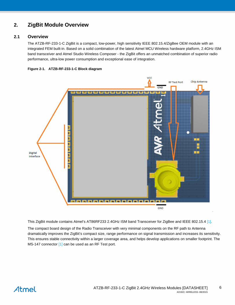
Figure 2-1. ATZB-RF-233-1-C Block diagram
.
This ZigBit module contains Atmel’s AT86RF233 2.4GHz ISM band Transceiver for ZigBee and IEEE 802.15.4 [1].
The compact board design of the Radio Transceiver with very minimal components on the RF path to Antenna dramatically improves the ZigBit’s compact size, range performance on signal transmission and increases its sensitivity. This ensures stable connectivity within a larger coverage area, and helps develop applications on smaller footprint. The MS-147 connector [1] can be used as an RF Test port.
ATZB-RF-233-1-C ZigBit 2.4GHz Wireless Modules [DATASHEET] 42192C−WIRELESS−08/2015
7
ZigBit Module contains a complete RF design with all the necessary passive components included. The module can be easily mounted on a simple 2-layer PCB with a minimum of required external connection. The ZigBit Module Evaluation kit containing the ZigBit Extension board for the Atmel Xplained PRO HW Evaluation platform can be used to develop FW using the Atmel Studio and evaluate using the Wireless Composer. Compared to a custom RF/MCU solution, a module-based solution offers considerable savings in development time and NRE cost per unit during the HW/FW design, prototyping, and mass production phases of product development.
Depending on end-user design requirements, the ZigBit can operate as a sensor node, where it can be paired with a host processor driving the module over a serial interface.
The MAC stack running on the host processor can then control data transmission. Thus very minimal firmware customization is required for successful module design-in. Third-party sensors can then be connected directly to the host MCU.
Every ZigBit Module come pre loaded with Atmel assigned 64-bit MAC address stored in the EEPROM built-in the module. This unique IEEE MAC address can be used as the MAC address of the end product, so there is no need to buy a MAC address separately for the product using the ZigBit.
ATZB-RF-233-1-C ZigBit 2.4GHz Wireless Modules [DATASHEET] 42192C−WIRELESS−08/2015
8
3. Specification
3.1 Electrical Characteristics
3.1.1 Absolute Maximum Ratings
Table 3-1. Absolute Maximum Ratings (1)(2)
Parameter Minimum Maximum
Voltage on any pin, except RESET with respect to ground -0.3V 3.6V (VDD max)
Input RF level +10dBm
Current into Vcc pins 200mA
Notes: 1. Absolute Maximum Ratings are the values beyond which damage to the device may occur. Under no circumstances must the absolute maximum ratings given in this table be violated. Stresses beyond those listed under "Absolute Maximum Ratings" may cause permanent damage to the device. This is a stress rating only. Functional operation of the device at these or other conditions, beyond those indicated in the operational sections of this specification, is not implied. Exposure to absolute maximum rating conditions for extended periods may affect device reliability.
2. Attention! ZigBit is an ESD-sensitive device. Precaution should be taken when handling the device in order to prevent permanent damage.
3.1.2 Power Supply
Table 3-2. Test Conditions (unless otherwise stated), Vcc = 3V, Tamb = 25°C.
Parameter Range Unit
Supply voltage, VDD 2.0 to 3.6 V
Current consumption: TX ON, FEM ON(1) 157 mA
Current consumption: RX ON, RPC, LNA Bypass 7.5 mA
Current consumption: RX ON, RPC, LNA ON 12.5 mA
Current consumption: RX ON, LNA ON 17 mA
Current consumption: TRX_OFF, FEM Sleep 337 µA
Sleep Current consumption: TRX Sleep, FEM Sleep 0.7 µA
Note 1: Output TX power (when measuring consumption in TX mode) is +19.4dBm.
Current consumption depends on multiple factors, including but not limited to, the board design and materials. When this module is assembled on a base board, the MCU current also should be considered in estimating Active and Sleep currents of the product
ATZB-RF-233-1-C ZigBit 2.4GHz Wireless Modules [DATASHEET] 42192C−WIRELESS−08/2015
9
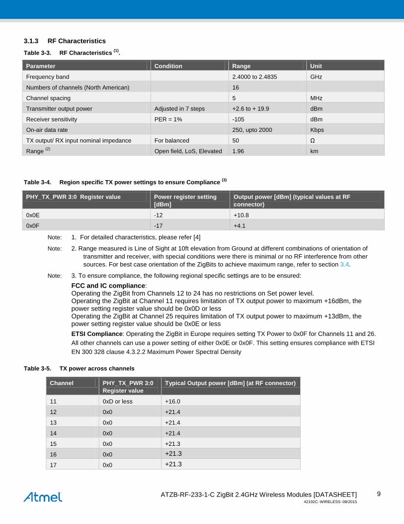
3.1.3 RF Characteristics
Table 3-3. RF Characteristics (1).
Parameter Condition Range Unit
Frequency band 2.4000 to 2.4835 GHz
Numbers of channels (North American) 16
Channel spacing 5 MHz
Transmitter output power Adjusted in 7 steps +2.6 to + 19.9 dBm
Receiver sensitivity PER = 1% -105 dBm
On-air data rate 250, upto 2000 Kbps
TX output/ RX input nominal impedance For balanced 50 Ω
Range (2) Open field, LoS, Elevated 1.96 km
Table 3-4. Region specific TX power settings to ensure Compliance (3)
PHY_TX_PWR 3:0 Register value Power register setting [dBm]
Output power [dBm] (typical values at RF connector)
0x0E -12 +10.8
0x0F -17 +4.1
Note: 1. For detailed characteristics, please refer [4]
Note: 2. Range measured is Line of Sight at 10ft elevation from Ground at different combinations of orientation of transmitter and receiver, with special conditions were there is minimal or no RF interference from other sources. For best case orientation of the ZigBits to achieve maximum range, refer to section 3.4.
Note: 3. To ensure compliance, the following regional specific settings are to be ensured: FCC and IC compliance: Operating the ZigBit from Channels 12 to 24 has no restrictions on Set power level. Operating the ZigBit at Channel 11 requires limitation of TX output power to maximum +16dBm, the power setting register value should be 0x0D or less Operating the ZigBit at Channel 25 requires limitation of TX output power to maximum +13dBm, the power setting register value should be 0x0E or less ETSI Compliance: Operating the ZigBit in Europe requires setting TX Power to 0x0F for Channels 11 and 26. All other channels can use a power setting of either 0x0E or 0x0F. This setting ensures compliance with ETSI EN 300 328 clause 4.3.2.2 Maximum Power Spectral Density
Table 3-5. TX power across channels
Channel PHY_TX_PWR 3:0 Register value
Typical Output power [dBm] (at RF connector)
11 0xD or less +16.0
12 0x0 +21.4
13 0x0 +21.4
14 0x0 +21.4
15 0x0 +21.3
16 0x0 +21.3
17 0x0 +21.3
ATZB-RF-233-1-C ZigBit 2.4GHz Wireless Modules [DATASHEET] 42192C−WIRELESS−08/2015
10
18 0x0 +21.3
19 0x0 +21.3
20 0x0 +21.3
21 0x0 +21.3
22 0x0 +21.3
23 0x0 +21.2
24 0x0 +21.1
25 0xE +13.0
26 0xE or less Restricted - Do not use in North America and Canada Restricted – Refer Note 2 for Europe
3.2 Physical/Environmental Characteristics and Outline
Table 3-6. Physical characteristics.
Parameters Value Comments
Size 25.0 x 20.0mm
Operating temperature range -40°C to +85°C -40°C to +85°C operational
3.3 Pin Configuration
Table 3-7. ATZB-RF-233-1-C Pinout description
Pin Out Pin descriptions
Function
1 AVSS Analog Ground 2 AVSS Analog Ground 3 DEVDD Digital Power input pin 4 DEVDD Digital Power input pin 5 /RST REST active low 6 /SEL SPI select, active low 7 MOSI SPI data input 8 MISO SPI data output 9 SCLK SPI clock
10 DIG1 Reserved 11 FEM_CSD Reserved 32 DIG3 RX TX Indication 33 DIG4 RX TX Indication (Inverted) 34 DIG2 Tx- Rx time-stamp 35 SLP_TR Controls sleep, deep sleep, transmit start, receive states; active high
ATZB-RF-233-1-C ZigBit 2.4GHz Wireless Modules [DATASHEET] 42192C−WIRELESS−08/2015
11
Pin Out Pin descriptions
Function
36 SCL TWI- EEPROM 37 SDA TWI- EEPROM 38 FEM_CPS Front end module select for RF_TX_RX 39 CLKM Master Clock out put 40 IRQ Interrupt request signal output 41 DVSS Digital Ground 42 DVSS Digital Ground
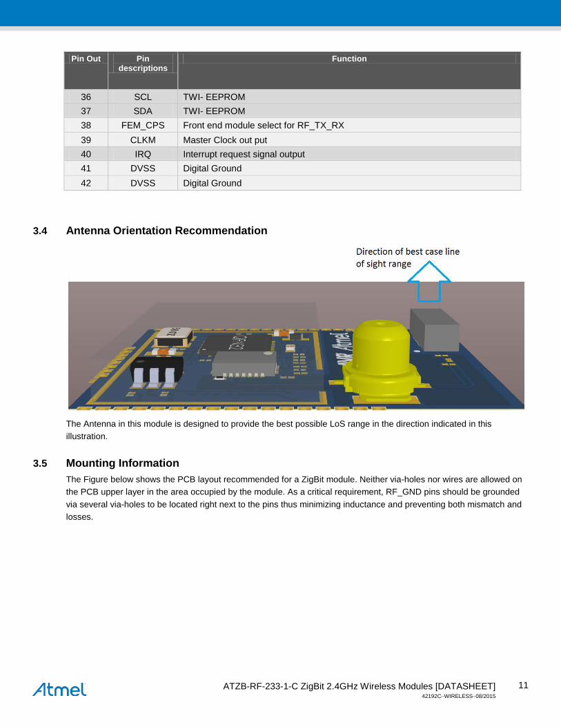
3.4 Antenna Orientation Recommendation
The Antenna in this module is designed to provide the best possible LoS range in the direction indicated in this illustration.
3.5 Mounting Information The Figure below shows the PCB layout recommended for a ZigBit module. Neither via-holes nor wires are allowed on the PCB upper layer in the area occupied by the module. As a critical requirement, RF_GND pins should be grounded via several via-holes to be located right next to the pins thus minimizing inductance and preventing both mismatch and losses.
ATZB-RF-233-1-C ZigBit 2.4GHz Wireless Modules [DATASHEET] 42192C−WIRELESS−08/2015
12
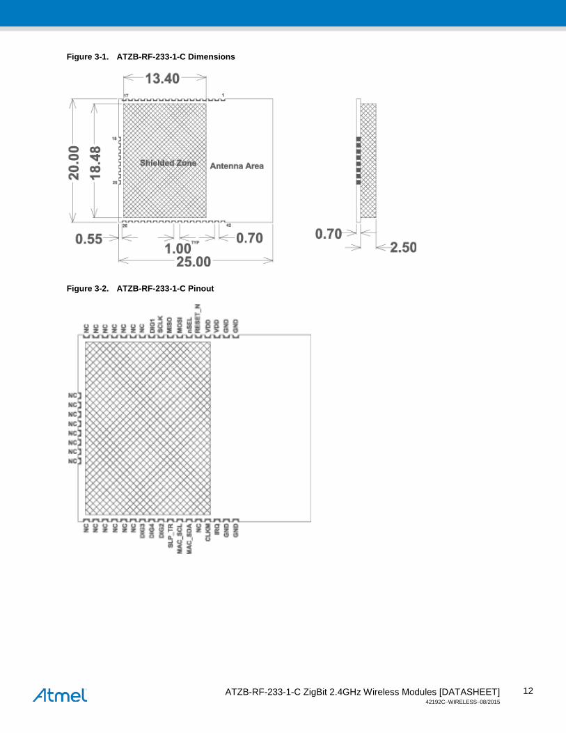
Figure 3-1. ATZB-RF-233-1-C Dimensions
Figure 3-2. ATZB-RF-233-1-C Pinout
ATZB-RF-233-1-C ZigBit 2.4GHz Wireless Modules [DATASHEET] 42192C−WIRELESS−08/2015
13
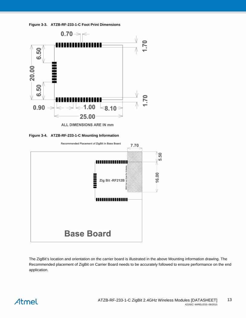
Figure 3-3. ATZB-RF-233-1-C Foot Print Dimensions
Figure 3-4. ATZB-RF-233-1-C Mounting Information
The ZigBit’s location and orientation on the carrier board is illustrated in the above Mounting information drawing. The Recommended placement of ZigBit on Carrier Board needs to be accurately followed to ensure performance on the end application.
ATZB-RF-233-1-C ZigBit 2.4GHz Wireless Modules [DATASHEET] 42192C−WIRELESS−08/2015
14
Please note the areas in the Mounting information drawing for copper and component keep out to ensure superior performance of the ZigBits on your End application. Copper keep out recommended in the drawing applies for all layers of the carrier board
The dimension A of the carrier board should be equal to or greater than 20mm. Similarly, the dimension B should be equal to or greater than 25mm
3.6 Soldering Profile The J-STD-020C-compliant soldering profile is recommended according to Table 3-8.
Table 3-8. Soldering profile(1)
Profile feature Green package
Average ramp-up rate (217°C to peak) 3°C/s max
Preheat temperature 175°C ±25°C 180s max
Temperature maintained above 217°C 60s to 150s
Time within 5°C of actual peak temperature 20s to 40s
Peak temperature range 260°C
Ramp-down rate 6°C/s max
Time within 25°C to peak temperature 8 minutes
Note: 1. The package is backward compatible with PB/Sn soldering profile.
3.7 Antenna Reference Designs Multiple factors affect proper antenna match, hence, affecting the antenna pattern. The particular factors are the board material and thickness, shields, the material used for enclosure, the board neighborhood, and other components adjacent to antenna. Following guidelines need to be followed when designing the base board for the ZigBit.
General Recommendations:
• Metal enclosure should not be used. Using low profile enclosure might also affect antenna tuning.
• Placing high profile components next to antenna should be avoided.
• Having holes/vias punched around the periphery of the board eliminates parasitic radiation from the board edges also distorting antenna pattern.
• ZigBit module should not be placed next to consumer electronics which might interfere with ZigBit’s RF band frequency.
The board design should prevent propagation of microwave field inside the board material. Electromagnetic waves of high frequency may penetrate the board thus making the edges of the board radiate, which may distort the antenna pattern. To eliminate this effect, metalized and grounded holes/vias must be placed around the board's edges.
4. Schematics The following schematic drawings for the ATZB-RF-233-1-C are in the following order:
• Top level schematics
• AT86RF233 schematics
ATZB-RF-233-1-C ZigBit 2.4GHz Wireless Modules [DATASHEET] 42192C−WIRELESS−08/2015
15
4.1 Handling Instructions The ZigBit Modules are fixed with an EMI Shield to ensure compliance to Emission and Immunity rules. This shield is galvanic and NOT air tight. So cleaning of the module with IPA / other similar agents is not advised. Humidity protection coating (conformal) will cause deviated RF behavior and coating material being trapped inside EMI Shield. So this should be avoided. For products requiring conformal coating, it is advised to suitably mask the ZigBit before applying the coating to rest of the ZigBit carrier board. To protect ZigBit from humidity, the housing of the product should ensure suitable Ingress Protection standards are complied with.
The MS-147 connector should never be exposed to Varnish / similar conformal coating material which will affect electrical connection on the surfaces of connector.
The in-built chip antenna has been tuned for the particular design
4.2 General Recommendations • Metal enclosure should not be used. Using low profile enclosure might also affect antenna tuning
• Placing high profile components next to antenna should be avoided
• Having holes/vias punched around the periphery of the board eliminates parasitic radiation from the board edges also distorting antenna pattern
• ZigBit module should not be placed next to consumer electronics which might interfere with ZigBit's RF frequency band
5. Persistence Memory A dedicated memory space is allocated to store product specific information and called the Persistence Memory. The organization of the persistence memory is as follows:
Table 5-1. Persistence Memory
Data Size
Structure Revision 2 bytes
MAC address(1) 8 bytes
Board information overall 49 bytes
Board information – PCBA Name 30 bytes
Board information – PCBA Serial number 10 bytes
Board information – PCBA Atmel Part Number 8 bytes
Board information – PCBA Revision 1 byte
Reserved 3 bytes
Xtal Calibration Value 1 byte
Reserved 7 bytes
Reserved 4 bytes
CRC 2 bytes
ATZB-RF-233-1-C ZigBit 2.4GHz Wireless Modules [DATASHEET] 42192C−WIRELESS−08/2015
16
ATZB-RF-233-1-C Zigbit contains AT24MAC602 which has a globally unique MAC address that can be assigned as the physical address of a system hardware device or node. Persistence memory is stored in the First-half of the Standard 2-Kbit EEPROM of AT24MAC602 starting from address 0x00.
Special commands are available to read the unique 64-bit MACID and the persistent memory via the I2C-compatible (2-wire) serial interface (see section "Device Addressing” in AT24MAC602 [5] for details).
Note: 1 The MAC address stored inside the AT24MAC602 is a uniquely assigned ID for each ZigBit and owned by Atmel. User of the ZigBit application can use this unique MAC ID to address the ZigBit in end-applications. The MAC ID can be read from the ZigBit using the Performance Analyzer Application that can be downloaded from www.atmel.com/wireless
6. Ordering Information Part number Description
ATZB-RF-233-1-C 2.4GHz IEEE802.15.4/ZigBee OEM module based on AT86RF233 Transceiver with MS-147 test connector and chip antenna, Single unit
ATZB-RF-233-1-CR 2.4GHz IEEE802.15.4/ZigBee OEM module based on AT86RF233 Transceiver with MS-147 test connector and chip antenna, Tape & Reel
Note: Tape and reel quantity: 200.
ATZB-RF-233-1-C ZigBit 2.4GHz Wireless Modules [DATASHEET] 42192C−WIRELESS−08/2015
17
7. Agency Certifications
7.1 United States (FCC) This equipment complies with Part 15 of the FCC rules and regulations. To fulfill FCC Certification requirements, an OEM manufacturer must comply with the following regulations:
The ATZB-RF-233-1-C modular transmitter must be labeled with its own FCC ID number, and, if the FCC ID is not visible when the module is installed inside another device, then the outside of the device into which the module is installed must also display a label referring to the enclosed module. This exterior label can use wording such as the following:
IMPORTANT: Contains FCC ID: VW4A091729. This equipment complies with Part 15 of the FCC Rules. Operation is subject to the following two conditions: (1) this device may not cause harmful interference, and (2) this device must accept any interference received, including interference that may cause undesired operation (FCC 15.19).
The internal antenna used for this mobile transmitter must provide a separation distance of at least 20 cm from all persons and must not be colocated or operating in conjunction with any other antenna or transmitter.
Installers must be provided with antenna installation instructions and transmitter operating conditions for satisfying RF exposure compliance. This device is approved as a mobile device with respect to RF exposure compliance, and may only be marketed to OEM installers. Use in portable exposure conditions (FCC 2.1093) requires separate equipment authorization.
IMPORTANT: Modifications not expressly approved by this company could void the user's authority to operate this equipment (FCC section 15.21).
IMPORTANT: This equipment has been tested and found to comply with the limits for a Class B digital device, pursuant to Part 15 of the FCC Rules. These limits are designed to provide reasonable protection against harmful interference when the equipment is operated in a commercial environment. This equipment generates, uses, and can radiate radio frequency energy and, if not installed and used in accordance with the instruction manual, may cause harmful interference to radio communications. Operation of this equipment in a residential area is likely to cause harmful interference in which case the user will be required to correct the interference at his own expense (FCC section 15.105).
7.2 European Union (ETSI) The ATZB-RF-233-1-C Module has been certified for use in European Union countries. If these modules are incorporated into a product, the manufacturer must ensure compliance of the final product to the European harmonized EMC and lowvoltage/safety standards. A Declaration of Conformity must be issued for each of these standards and kept on file as described in Annex II of the R&TTE Directive.
Furthermore, the manufacturer must maintain a copy of the modules' documentation and ensure the final product does not exceed the specified power ratings, antenna specifications, and/or installation requirements as specified in the user manual. If any of these specifications are exceeded in the final product, a submission must be made to a notified body for compliance testing to all required standards.
ATZB-RF-233-1-C ZigBit 2.4GHz Wireless Modules [DATASHEET] 42192C−WIRELESS−08/2015
18
IMPORTANT: The 'CE' marking must be affixed to a visible location on the OEM product. The CE mark shall consist of the initials "CE" taking the following form:
The CE marking must have a height of at least 5mm except where this is not possible on account of the nature of the apparatus.
The CE marking must be affixed visibly, legibly, and indelibly.
More detailed information about CE marking requirements you can find at "DIRECTIVE 1999/5/EC OF THE EUROPEAN PARLIAMENT AND OF THE COUNCIL" on 9 March 1999 at section 12.
7.3 Canada (IC) This device complies with Industry Canada licence-exempt RSS standard(s). Operation is subject to the following two conditions: (1) this device may not cause interference, and (2) this device must accept any interference, including interference that may cause undesired operation of the device. Le présent appareil est conforme aux CNR d'Industrie Canada applicables aux appareils radio exempts de licence. L'exploitation est autorisée aux deux conditions suivantes: (1) l'appareil ne doit pas produire de brouillage, et (2) l'utilisateur de l'appareil doit accepter tout brouillage radioélectrique subi, même si le brouillage est susceptible d'en compromettre le fonctionnement. This equipment complies with radio frequency exposure limits set forth by Industry Canada for an uncontrolled environment. This equipment should be installed and operated with minimum distance 20 cm between the device and the user or bystanders. Cet équipement est conforme aux limites d'exposition aux radiofréquences définies par Industrie Canada pour un environnement non contrôlé. Cet équipement doit être installé et utilisé avec un minimum de 20 cm de distance entre le dispositif et l'utilisateur ou des tiers CAUTION: Any changes or modifications not expressly approved by the party responsible for compliance could void the user’s authority to operate the equipment. The OEM integrator is still responsible for testing their end-product for any additional compliance requirements required with this module installed (for example, digital device emissions, PC peripheral requirements, etc.). This Module is labelled with its own IC ID. If the IC ID Certification Number is not visible while installed inside another device, then the device should display the label on it referring the enclosed module. In that case, the final end product must be labelled in a visible area with the following: “Contains Transmitter Module IC:11019A-091729” OR “Contains IC: 11019A-091729” Ce module est étiqueté avec son propre ID IC. Si le numéro de certification IC ID n'est pas visible lorsqu'il est installé à l'intérieur d'un autre appareil, l'appareil doit afficher l'étiquette sur le module de référence ci-joint. Dans ce cas, le produit final doit être étiqueté dans un endroit visible par le texte suivant: “Contains Transmitter Module IC: 11019A-091729” OR “Contains IC: 11019A-091729”
ATZB-RF-233-1-C ZigBit 2.4GHz Wireless Modules [DATASHEET] 42192C−WIRELESS−08/2015
19
8. Revision History Doc. Rev. Date Comments
42192C 08/2015 • Updated the table note Note 3: This setting ensures compliance with ETSI EN 300 328 clause 4.3.2.2 Maximum Power Spectral Density
42192B 03/2014 • Updated the mounting information drawimg Figure 3-4 • Updated the section “Persistence”
42192A 11/2013 Initial revision.

Atmel Corporation 1600 Technology Drive San Jose, CA 95110 USA Tel: (+1)(408) 441-0311 Fax: (+1)(408) 487-2600 www.atmel.com
Atmel Asia Limited Unit 01-5 & 16, 19F BEA Tower, Millennium City 5 418 Kwun Tong Road Kwun Tong, Kowloon HONG KONG Tel: (+852) 2245-6100 Fax: (+852) 2722-1369
Atmel Munich GmbH Business Campus Parkring 4 D-85748 Garching b. Munich GERMANY Tel: (+49) 89-31970-0 Fax: (+49) 89-3194621
Atmel Japan G.K. 16F Shin-Osaki Kangyo Building 1-6-4 Osaki, Shinagawa-ku Tokyo 141-0032 JAPAN Tel: (+81)(3) 6417-0300 Fax: (+81)(3) 6417-0370
© 2015 Atmel Corporation. All rights reserved. / Rev.: 42192C−WIRELESS−08/2015
Atmel®, Atmel logo and combinations thereof, Enabling Unlimited Possibilities®, AVR®, ZigBit®, and others are registered trademarks or trademarks of Atmel Corporation or its subsidiaries. Other terms and product names may be trademarks of others.
Disclaimer: The information in this document is provided in connection with Atmel products. No license, express or implied, by estoppel or otherwise, to any intellectual property right is granted by this document or in connection with the sale of Atmel products. EXCEPT AS SET FORTH IN THE ATMEL TERMS AND CONDITIONS OF SALES LOCATED ON THE ATMEL WEBSITE, ATMEL ASSUMES NO LIABILITY WHATSOEVER AND DISCLAIMS ANY EXPRESS, IMPLIED OR STATUTORY WARRANTY RELATING TO ITS PRODUCTS INCLUDING, BUT NOT LIMITED TO, THE IMPLIED WARRANTY OF MERCHANTABILITY, FITNESS FOR A PARTICULAR PURPOSE, OR NON-INFRINGEMENT. IN NO EVENT SHALL ATMEL BE LIABLE FOR ANY DIRECT, INDIRECT, CONSEQUENTIAL, PUNITIVE, SPECIAL OR INCIDENTAL DAMAGES (INCLUDING, WITHOUT LIMITATION, DAMAGES FOR LOSS AND PROFITS, BUSINESS INTERRUPTION, OR LOSS OF INFORMATION) ARISING OUT OF THE USE OR INABILITY TO USE THIS DOCUMENT, EVEN IF ATMEL HAS BEEN ADVISED OF THE POSSIBILITY OF SUCH DAMAGES. Atmel makes no representations or warranties with respect to the accuracy or completeness of the contents of this document and reserves the right to make changes to specifications and products descriptions at any time without notice. Atmel does not make any commitment to update the information contained herein. Unless specifically provided otherwise, Atmel products are not suitable for, and shall not be used in, automotive applications. Atmel products are not intended, authorized, or warranted for use as components in applications intended to support or sustain life.
Recommended

![ZigBit 2.4GHz Wireless Modules ATZB-24-A2/B0 · ATZB-X0-256-4-0-CN [ZigBit 900MHz Wireless Modules] 42268A−WIRELESS−04/2014 4 HW Hardware I2C Inter-Integrated Circuit IEEE …](https://img.pdfslide.net/doc/110x75/5b0d81707f8b9a952f8d9887/zigbit-24ghz-wireless-modules-atzb-24-a2b0-zigbit-900mhz-wireless-modules-42268awireless042014.jpg)
![ZigBit Extension User Guide (USER GUIDE) · ZigBit Extension User Guide [USER GUIDE] 42186C-MCU-07/2014 4 1.3.3 In Customer Development Assembly The Extension board can be wired into](https://img.pdfslide.net/doc/110x75/5eb92de63153f825911b85ba/zigbit-extension-user-guide-user-guide-zigbit-extension-user-guide-user-guide.jpg)

![Módulo OEM ZigBit 900 - Nextfor - ZigBit 900.pdf · plataforma hardware AVR Z-Link de Atmel [1], el ZigBit 900 ofrece una prestación de radio superior con una excepcional facilidad](https://img.pdfslide.net/doc/110x75/5e9297195970022bd57a76cc/mdulo-oem-zigbit-900-zigbit-900pdf-plataforma-hardware-avr-z-link-de-atmel.jpg)