Bipolar Junction TransistorBy:
Engr. Syed Asad Ali
AcknowledgementLarge Part Of This Lecture is Taken From Manipal Institute India
BASIC ELECTRONICS

Lecture Contents• Introduction to Bipolar Junction Transistor• BJT Operation• BJT Configurations• Transistor Application• BJT Biasing

Introduction• Solid state transistor was invented by a team of scientists at Bell laboratories during 1947-48• It brought an end to vacuum tube era• Advantages of solid state transistor over vacuum devices:
– Smaller size, light weight– No heating elements required– Lower power consumption and operating voltages– Low price
Introduction
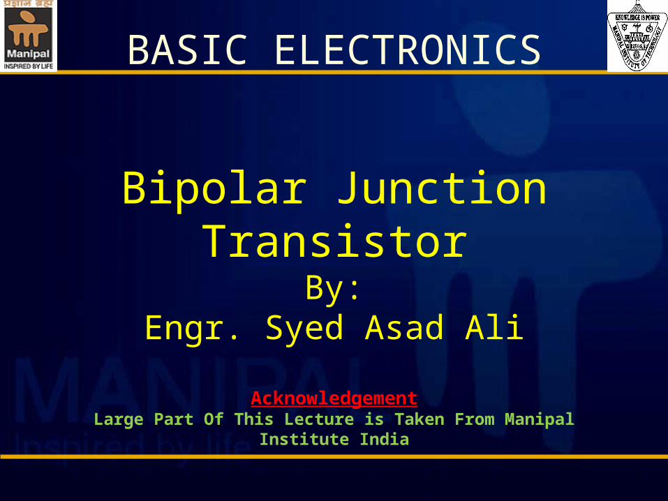
Figure showing relative sizes of transistor, IC and LED
Figure showing different transistor packages
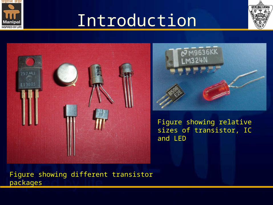
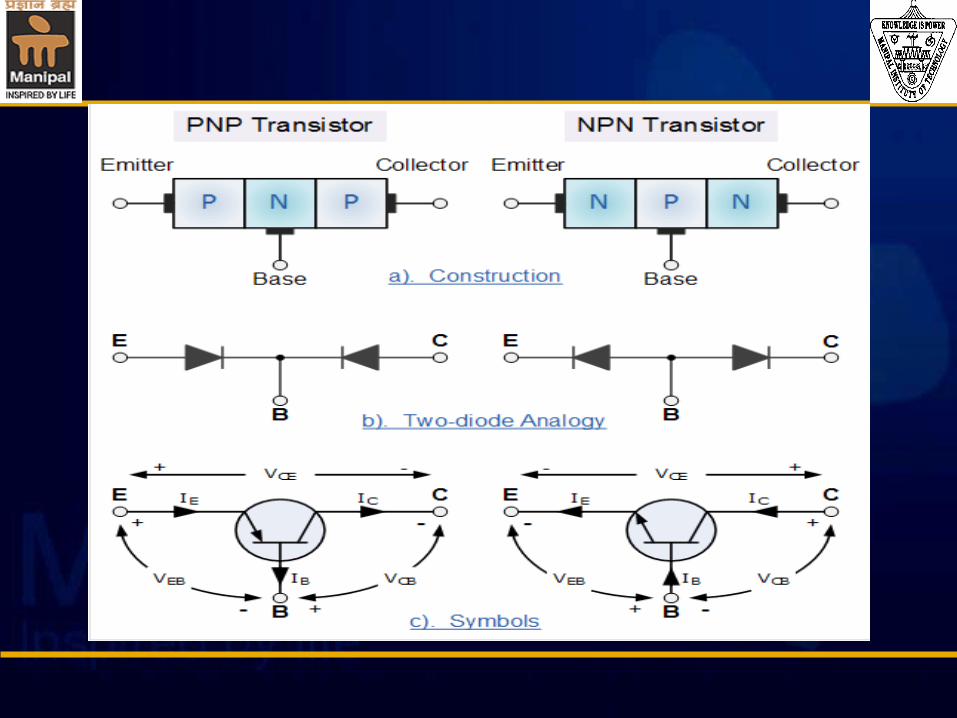
Introduction• Bipolar Junction Transistor (BJT) is a sandwich consisting of three layers of two different types of semiconductor • Two kinds of BJT sandwiches are: NPN and PNP
Introduction• The three layers of BJT are called Emitter, Base and Collector• Base is very thin compared to the other two layers• Base is lightly doped. Emitter is heavily doped. Collector is moderately doped• NPN – Emitter and Collector are made of N-type semiconductors; Base is P-type• PNP – Emitter and Collector are P-type, Base is N-type• Both types (NPN and PNP) are extensively used, either separately or in the same circuit
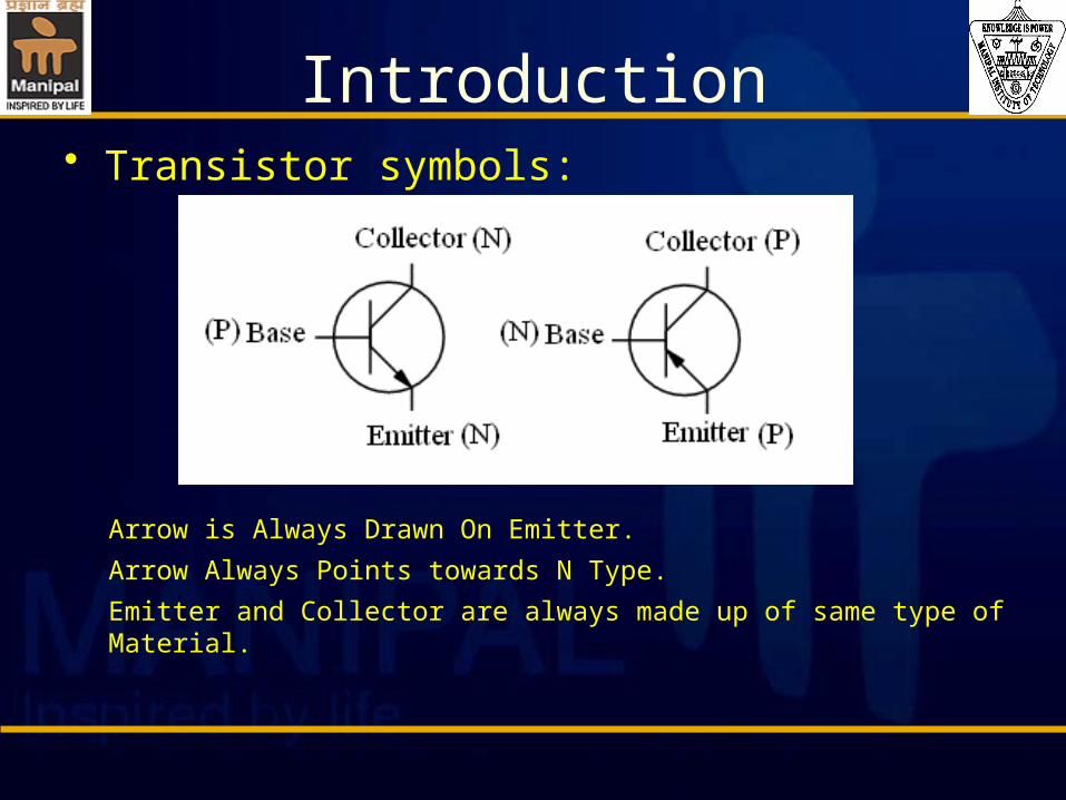
Introduction• Transistor symbols:
Arrow is Always Drawn On Emitter.
Arrow Always Points towards N Type.
Emitter and Collector are always made up of same type of Material.
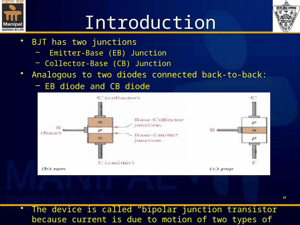
Introduction• BJT has two junctions
– Emitter-Base (EB) Junction– Collector-Base (CB) Junction
• Analogous to two diodes connected back-to-back: – EB diode and CB diode
• The device is called “bipolar junction transistor” because current is due to motion of two types of charge carriers – free electrons & holes

Transistor Operation• Three Mode Of Operation
Transistor Operation• Operation of NPN transistor is discussed here; operation of PNP is similar with roles of free electrons and holes interchanged• For normal operation (amplifier application)
– EB junction should be forward biased – CB junction should be reverse biased
• Depletion width at EB junction is narrow (forward biased)• Depletion width at CB junction is wide (reverse biased)
Department of Electronics and Communication Engineering,Manipal Institute of Technology, Manipal, INDIA

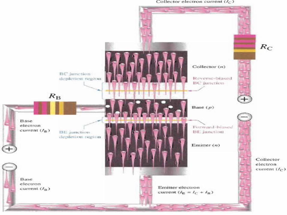
Transistor Operation• When EB junction is forward biased, free electrons from emitter region drift towards base region.• Base is Thin and Lightly Doped, hence have very minimum Holes.• Only small percentage of Emitter free electrons combine with holes in the base to form small base current. • While majority of the free electrons are swept away into the collector region due to reverse biased CB junction.
Transistor Operation
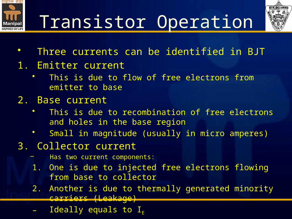
• Three currents can be identified in BJT
1. Emitter current • This is due to flow of free electrons from emitter to base
2. Base current• This is due to recombination of free electrons and holes in the base
region• Small in magnitude (usually in micro amperes)
3. Collector current– Has two current components:
1. One is due to injected free electrons flowing from base to collector
2. Another is due to thermally generated minority carriers (Leakage)
– Ideally equals to IE
Transistor Operation
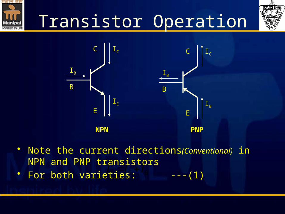
• Note the current directions(Conventional) in NPN and PNP transistors
• For both varieties: ---(1)
C
E
B
IC
IE
IB
NPN
C
E
B
IC
IE
IB
PNP
BCE III
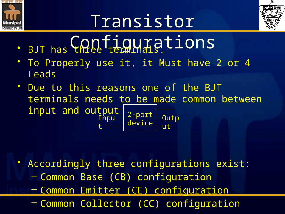
Transistor Configurations• BJT has three terminals.• To Properly use it, it Must have 2 or 4 Leads • Due to this reasons one of the BJT terminals needs to be made
common between input and output
• Accordingly three configurations exist:– Common Base (CB) configuration– Common Emitter (CE) configuration– Common Collector (CC) configuration
Input Output2-port device
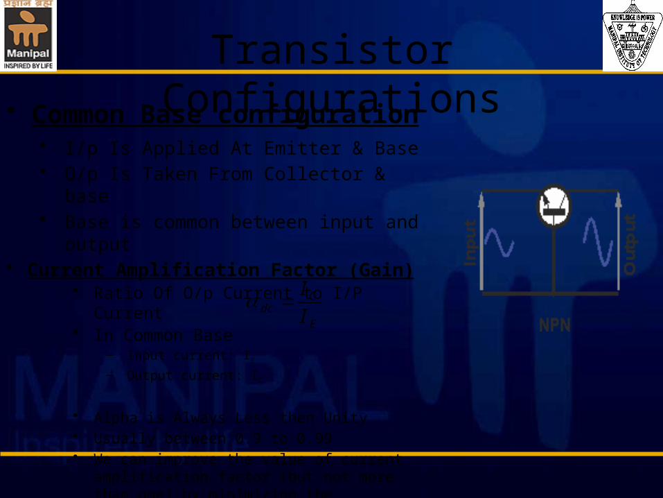
Transistor Configurations• Common Base configuration
• I/p Is Applied At Emitter & Base• O/p Is Taken From Collector & base• Base is common between input and output
• Current Amplification Factor (Gain)• Ratio Of O/p Current to I/P Current• In Common Base
– Input current: IE
– Output current: IC
• Alpha is Always Less then Unity• Usually between 0.9 to 0.99• We can improve the value of current amplification factor
(but not more than one) by minimizing the recombination in the base and this is achieved by doping the base very lightly and making it very thin.
E
Cdc I
I
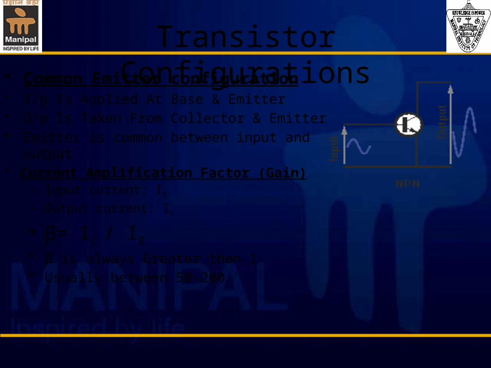
Transistor Configurations• Common Emitter configuration• I/p Is Applied At Base & Emitter• O/p Is Taken From Collector & Emitter• Emitter is common between input and output• Current Amplification Factor (Gain)
– Input current: IB
– Output current: IC
• β= IC / IB
• β is always Greater then 1• Usually between 50-200

Transistor Configurations
• Common Collector configuration– I/p Is Applied At Base & Collector– O/p Is Taken From Emitter & Collector– Collector is common between input and
output– Current Amplification Factor
• Input current: IB
• Output current: IC
• γ =IE/IB
As IE=IC so Above Formula Will be equal to Beta, Hence C.C provide same Current Gain As C.B
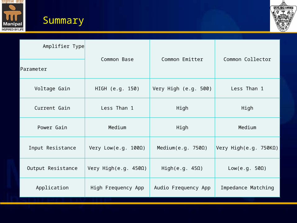
Amplifier Type
Common Base Common Emitter Common Collector
Parameter
Voltage Gain HIGH (e.g. 150) Very High (e.g. 500) Less Than 1
Current Gain Less Than 1 High High
Power Gain Medium High Medium
Input Resistance Very Low(e.g. 100Ω) Medium(e.g. 750Ω) Very High(e.g. 750KΩ)
Output Resistance Very High(e.g. 450Ω) High(e.g. 45Ω) Low(e.g. 50Ω)
Application High Frequency App Audio Frequency App Impedance Matching
Summary

Transistor Application
1. Transistor As Amplifier
2. Transistor As a Switch
Transistor As Amplifier
• Amplification is the process of linearly increasing the strength of electrical signal
• Weak Signal Is Applied at the Input and Amplified(Strong Signal Is Collected at the Output)
• For amplifier application, transistor should operate in Active Region
Transistor As Switch• When Transistor is Operated as A switch it is normally Operated in
Cutoff & Saturation Mode• Conditions For Cutoff
– B.E Junction Is Reverse Bias • No Input Current
– B.C Junction Is Reverse Bias• No Output Current or No Collector Current
– Neglecting Leakage Current
– Transistor Behave as Open Switch• Condition For Saturation
– B.E & B.C Junction Is Forward Bias – Maximum Or Large Input (base)Current – Maximum Output Current (Collector Current )– Transistor Behave as Close Switch
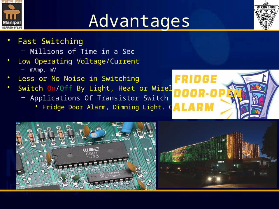
Advantages• Fast Switching
– Millions of Time in a Sec• Low Operating Voltage/Current
– mAmp, mV
• Less or No Noise in Switching• Switch On/Off By Light, Heat or Wireless Signal
– Applications Of Transistor Switch• Fridge Door Alarm, Dimming Light, Computers
Transistor Biasing• What is meant by biasing the transistor?
– Applying external dc voltages to ensure that transistor operates in the desired region/Mode
• Which is the desired region?– For amplifier application, transistor should operate in
Active Region– For switch application, it should operate in cut-off and saturation.
Types of biasing: 1. Base Bias2. Emitter Bias 3. Voltage Divider Bias
Transistor Biasing• Base Bias
– Pros: Simple circuit
Uses very few resistors
– Cons: This Circuit is unstable • Parameters can be changed with Temperature & from Transistor to
Transistors
Transistor Biasing
• Emitter Bias: • Pros:
• Good stability compares to Base Bias
– Cons:• This type can only be used when a split (dual) power supply
is available (Costly $)
Transistor Biasing
• Voltage Divider:– Pros: Unlike above circuits, only one dc supply is necessary.– Stable Circuit
– Cons:• Circuit Analysis Is Complex• Requires Many Components (Resistors)
Recommended