×
Log in
Upload File
Most Popular
Art & Photos
Automotive
Business
Career
Design
Education
Hi-Tech
+ Browse for More
Download pdf -
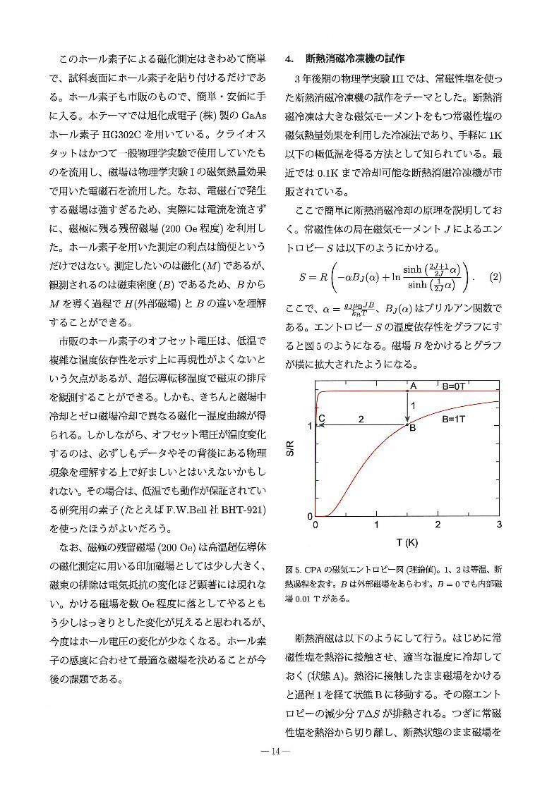
B=OT B=IT CD 5. CPA 2 0.01 T l.JTfiö0 TAS 14 VdD 2 VdD 2 VdD NCO (YdD) • E È C02 K YdD Created Date 2/7/2011 4:00:58 PM
Download pdf
Transcript
Page 1
Page 2
Page 3
Page 4
Page 5
LOAD MORE
Recommended
IS42R32160F, IS45R32160F IS42S32160F, IS45S32160F• Power supply: Vdd/Vddq = 2.3V-3.6V IS42/45S32160F - Vdd/Vddq = 3.3V IS42/45R32160F - Vdd/Vddq = 2.5 • LVTTL interface • Programmable
Documents
AMD S1 PROCESSOR UNBUFFERED DDR2 NEAR EXTERNAL … · 2017. 4. 26. · sc413 vdd adapter & battery selector +5vsus pwr_src oz826ln sm bus to kbc vdd vdd ac_ok# vdd inverter cpu_vdd_run
Documents
SSO Simulation with IBIS · kpd(t)*Ipd(Vout) Ipc(Vout) Igc(Vout) C_comp/2 C_comp/2 OUT VSS VDD td_RCr(Vdd-Vss) * td_RCf(Vdd-Vss) * td_RC determination-by optimisation through the
Documents
SiT8008 - SiTime · 90% Vdd, 2.5/2,8/3.3V devices 95% Vdd, 1.8V devices Vdd Pin 4 Voltage CLK Output T_start T_start: Time to start from power-off NO Glitch first cycle 50% Vdd Vdd
Documents
CMOS: conceptes bàsics · 2012. 9. 5. · Tecnologia MOSTecnologia MOS • Inversor CMOS: Complementary MOSInversor CMOS: Complementary MOS Input Output D 1 (VDD) 1 (VDD) 1 (VDD)
Documents
Evaluation Kit User’s Manual - pSemi › pdf › eval_kit › manual › pe43705man.pdf · A2_2 A2 A2_1 VDD A1_1 VDD A0_1 VDD HDR4 HEADER3X3 1 2 HDR1 HEADER 1X2 1 1 2 2 HDR3 HEADER
Documents
Rahway Steel Drum | Your Reliable Source for Drums and Drum …€¦ · xxx xxx-6L suompuoo -LC-Vdd -LC-Ydd papuewwooea s! woo O!1Seld pue :a10N we) ueno 01 pasodxa eq Iou Isnw sônld
Documents
LMH0318 Programming Guide - Texas Instruments · 1 kΩto VDD 20 kΩto GND 11 01 1A 34 1 kΩto VDD Float 11 10 1B 36 1 kΩto VDD 1 kΩto VDD 11 11 1C 38 (1)
Documents
Untitled Document [] · to IC Unless otherwise indicated, all limits are specified for VDD = +2.7V to +5.5V, VSS = GND, TA = 25 °C, VCM = VDD/2, RL = 100kΩ to VDD/2, and VOUT ~
Documents
PACIFIC DISPLAY DEVICES · PACIFIC DISPLAY DEVICES 11.02.2007 2 ... Parameter Symbol Min Max Unit Supply voltage for logic VDD-0.3 7.0 V Supply voltage for LCD VDD – Vo VDD –
Documents
ydd kaPsamında sÜrdÜrÜlebİlİr yaPı malZemesİ kUllanımı
Documents
TECH. CORP. · 1.6 Backlight & LED Characteristics 2. MODULE STRUCTURE 2.1 Counter Drawing ... LCD Driver Supply Voltage VLCD - VDD-10.0 VDD+0.3 V ... Process improvement proposal
Documents
VOLTAGE-C C O (VCXO) - Silicon Labs · Control Voltage Range VC 0.1 x VDD VDD/2 0.9 x VDD V Control Voltage Tuning Slope (10 to 90% VDD) Kv Positive slope ... 0.55 0.8 0.90 VPPSE
Documents
High Speed Op-amp Design: Compensation and Topologies for ... compens… · Amplifier Blocks. (Compensation not shown here) 1 VDD VDD V biasn v m v p VDD C L v out 2 VDD VDD V biasn
Documents
3.1 Circuito digital básico: El inversor CMOS.personales.unican.es/solanaj/m1_para_web_2011/TEMAS_micro_I/Micro_I... · tot *VDD 2)/T=(C tot *VDD 2)*f clk I avg = Q tot /T=(C tot
Documents
CMT-HADES2P Version: Preliminary Datasheet (Last ... · ckb comp vdd vdd vref vref vin +-+-threshold swt vin vdd fb comp uvlo pvdd drain pgnd vdd gnd ... lp filter rx (200ns) + +
Documents
K200CCNN-N13 · Unit Note Supply voltage VDD -0.3 +4.3 V 1 Input voltage Vin -0.3 VDD+0.3 V Note: 1.VDD, GND must be maintained. 2.The modules may be destroyed if they are used beyond
Documents
16 80Msps/65Msps ADC · VIH High Level Input Voltage VDD = 3.3V l 2 V VIL Low Level Input Voltage VDD = 3.3V l 0.8 V IIN Digital Input Current VIN = 0V to VDD l ±10 µA CIN Digital
Documents


![Untitled Document [] · to IC Unless otherwise indicated, all limits are specified for VDD = +2.7V to +5.5V, VSS = GND, TA = 25 °C, VCM = VDD/2, RL = 100kΩ to VDD/2, and VOUT ~](https://img.pdfslide.net/doc/110x75/5e7405a09fd2db4c0a486c73/untitled-document-to-ic-unless-otherwise-indicated-all-limits-are-specified.jpg)