Seiko Instruments Inc. 1
BUILT-IN DELAY CIRCUIT HIGH-PRECISION VOLTAGE DETECTOR S-809 Series
The S-809 Series is a high-precision voltage detector developed usingCMOS process. The detection voltage is fixed internally, with anaccuracy of ±2.0%. Attachment of an external capacitor can delay therelease signal. Two output types, Nch open-drain and CMOS output,are available.
n Features n Applications
• Ultra-low current consumption • Battery checker
1.0 µA typ. (VDD=2.0 V) • Power failure detector
; Products with a detection voltage of 1.4 V or less • Power monitor for portable equipment such as
1.2 µA typ. (VDD=3.5 V) pagers, electric calculators, electric notes and
; Products with a detection voltage of 1.5 V or more remote controllers
• High-precision detection voltage • Constant voltage power monitor for cameras,
±2.0% video equipment and communication devices
• Low operating voltage • Power monitor for microcomputers and reset for
0.80 to 6.0 V CPUs
; Products with detection voltage of 1.4 V or less
0.95 to 10.0 V
; Products with detection voltage of 1.5 V or more
• Hysteresis characteristics n Pin Assignment 5% typ
• Detection voltage
1.1 to 6.0 V
(0.1V step)
• Nch open-drain active low and CMOS active low output
• SOT-23-5 Very-small plastic package
Figure 1
n Block Diagram
(1) Nch open-drain active low output (2) CMOS active low output
Figure 2
1 OUT
2 VDD
3 VSS
4 NC
5 CD
SOT-23-5
Top view
1 2 3
5 4
2
5
3
1Delaycircuit
OUT
CD
VREF
VSS
VDD
*
*
*Parasitic diode
2
5
3
1Delaycircuit
OUT
CD
VREF
VSS
VDD
*
Rev. 2.0

BUILT-IN DELAY CIRCUIT HIGH-PRECISION VOLTAGE DETECTORS-809 Series
2 Seiko Instruments Inc.
n Selection Guide
S−80915 AN MP − DDC − T2
Directions of the IC for taping specifications
Product name (abbreviation)
Package name (abbreviation)
MP:SOT-23-5
Output type
N:Nch open-drain (active low output)
L:CMOS (active low output)
Detection voltage rank
Table 1Detection voltage range (V) Hysteresis width
VHYS typ.(V)Nch Open Drain(Low) CMOS Output(Low)
1.1V±2.0% 0.055 S-80911ANMP-D71-T2 S-80911ALMP-D51-T2
1.2V±2.0% 0.060 S-80912ANMP-D72-T2 S-80912ALMP-D52-T2
1.3V±2.0% 0.065 S-80913ANMP-DDA-T2 S-80913ALMP-DAA-T2
1.4V±2.0% 0.070 S-80914ANMP-DDB-T2 S-80914ALMP-DAB-T2
1.5V±2.0% 0.075 S-80915ANMP-DDC-T2 S-80915ALMP-DAC-T2
1.6V±2.0% 0.080 S-80916ANMP-DDD-T2 S-80916ALMP-DAD-T2
1.7V±2.0% 0.085 S-80917ANMP-DDE-T2 S-80917ALMP-DAE-T2
1.8V±2.0% 0.090 S-80918ANMP-DDF-T2 S-80918ALMP-DAF-T2
1.9V±2.0% 0.095 S-80919ANMP-DDG-T2 S-80919ALMP-DAG-T2
2.0V±2.0% 0.100 S-80920ANMP-DDH-T2 S-80920ALMP-DAH-T2
2.1V±2.0% 0.105 S-80921ANMP-DDJ-T2 S-80921ALMP-DAJ-T2
2.2V±2.0% 0.110 S-80922ANMP-DDK-T2 S-80922ALMP-DAK-T2
2.3V±2.0% 0.115 S-80923ANMP-DDL-T2 S-80923ALMP-DAL-T2
2.4V±2.0% 0.120 S-80924ANMP-DDM-T2 S-80924ALMP-DAM-T2
2.5V±2.0% 0.125 S-80925ANMP-DDN-T2 S-80925ALMP-DAN-T2
2.6V±2.0% 0.130 S-80926ANMP-DDP-T2 S-80926ALMP-DAP-T2
2.7V±2.0% 0.135 S-80927ANMP-DDQ-T2 S-80927ALMP-DAQ-T2
2.8V±2.0% 0.140 S-80928ANMP-DDR-T2 S-80928ALMP-DAR-T2
2.9V±2.0% 0.145 S-80929ANMP-DDS-T2 S-80929ALMP-DAS-T2
3.0V±2.0% 0.150 S-80930ANMP-DDT-T2 S-80930ALMP-DAT-T2
3.1V±2.0% 0.155 S-80931ANMP-DDV-T2 S-80931ALMP-DAV-T2
3.2V±2.0% 0.160 S-80932ANMP-DDW-T2 S-80932ALMP-DAW-T2
3.3V±2.0% 0.165 S-80933ANMP-DDX-T2 S-80933ALMP-DAX-T2
3.4V±2.0% 0.170 S-80934ANMP-DDY-T2 S-80934ALMP-DAY-T2
3.5V±2.0% 0.175 S-80935ANMP-DDZ-T2 S-80935ALMP-DAZ-T2
3.6V±2.0% 0.180 S-80936ANMP-DD0-T2 S-80936ALMP-DA0-T2
3.7V±2.0% 0.185 S-80937ANMP-DD1-T2 S-80937ALMP-DA1-T2
3.8V±2.0% 0.190 S-80938ANMP-DD2-T2 S-80938ALMP-DA2-T2
3.9V±2.0% 0.195 S-80939ANMP-DD3-T2 S-80939ALMP-DA3-T2
4.0V±2.0% 0.200 S-80940ANMP-DD4-T2 S-80940ALMP-DA4-T2
4.1V±2.0% 0.205 S-80941ANMP-DD5-T2 S-80941ALMP-DA5-T2
4.2V±2.0% 0.210 S-80942ANMP-DD6-T2 S-80942ALMP-DA6-T2
4.3V±2.0% 0.215 S-80943ANMP-DD7-T2 S-80943ALMP-DA7-T2
4.4V±2.0% 0.220 S-80944ANMP-DD8-T2 S-80944ALMP-DA8-T2
4.5V±2.0% 0.225 S-80945ANMP-DD9-T2 S-80945ALMP-DA9-T2
4.6V±2.0% 0.230 S-80946ANMP-DJA-T2 S-80946ALMP-DEA-T2
4.7V±2.0% 0.235 S-80947ANMP-DJB-T2 S-80947ALMP-DEB-T2
4.8V±2.0% 0.240 S-80948ANMP-DJC-T2 S-80948ALMP-DEC-T2
4.9V±2.0% 0.245 S-80949ANMP-DJD-T2 S-80949ALMP-DED-T2
5.0V±2.0% 0.250 S-80950ANMP-DJE-T2 S-80950ALMP-DEE-T2
5.1V±2.0% 0.255 S-80951ANMP-DJF-T2 S-80951ALMP-DEF-T2
5.2V±2.0% 0.260 S-80952ANMP-DJG-T2 S-80952ALMP-DEG-T2
5.3V±2.0% 0.265 S-80953ANMP-DJH-T2 S-80953ALMP-DEH-T2
5.4V±2.0% 0.270 S-80954ANMP-DJJ-T2 S-80954ALMP-DEJ-T2
5.5V±2.0% 0.275 S-80955ANMP-DJK-T2 S-80955ALMP-DEK-T2
5.6V±2.0% 0.280 S-80956ANMP-DJL-T2 S-80956ALMP-DEL-T2
5.7V±2.0% 0.285 S-80957ANMP-DJM-T2 S-80957ALMP-DEM-T2
5.8V±2.0% 0.290 S-80958ANMP-DJN-T2 S-80958ALMP-DEN-T2
5.9V±2.0% 0.295 S-80959ANMP-DJP-T2 S-80959ALMP-DEP-T2
6.0V±2.0% 0.300 S-80960ANMP-DJQ-T2 S-80960ALMP-DEQ-T2

BUILT-IN DELAY DIRCUIT HIGH-PRECISION VOLTAGE DETECTOR S-809 Series
Seiko Instruments Inc. 3
n Output Configurations
1. S-809 Series model numbering system
Nch open-drain(“L” reset type)
CMOS output(“L” reset type)
S-809 Series“N” is the last letter of themodel number.e.g. S-80915AN
“L” is the last letter of themodel number.e.g. S-80915AL
2. Output configurations and their implementation
Implementation Nch(“L”) CMOS(“L”)
With different power supplies Yes NoWith active low reset CPUs Yes YesWith active high reset CPUs No NoWith voltage divider variable resistors Yes No
Example with two power supplies Examples with one power supply
VSS
OUTCPU
VDD2VDD1
V/DNch
CD
VSS
OUTCPU
VDD
V/DCMOS
CD
VSS
OUTCPU
VDD
V/DNch
CD
Figure 3
n Advantage over the S-808 Series
1. Built-In delay circuit
Delay time setting by an additional external capacitor:
The S-809 can easily delay an release signal by attachment of an external capacitor with built-In delay circuit.
This results in an advantage of parts reduction over the S-808 Series.

BUILT-IN DELAY CIRCUIT HIGH-PRECISION VOLTAGE DETECTORS-809 Series
4 Seiko Instruments Inc.
n Absolute Maximum Ratings
1. Products with a Detection voltage of 1.4V or less.
(Unless otherwise specified:Ta=25°C)Parameter Symbol Ratings Unit
Power supply voltage VDD−VSS 8 V
CD terminal Input voltage VCD VSS-0.3 to VDD +0.3 V
Outputvoltage
Nchopen-drain VOUT VSS-0.3 to 8 V
CMOS VSS-0.3 to VDD+0.3 VOutput current IOUT 50 mAPower dissipation Pd 150 mWOperating temperature Topr −40 to +85 °CStorage temperature Tstg −40 to +125 °C
2. Products with a Detection voltage of 1.5V or more.
(Unless otherwise specified: Ta=25°C)Parameter Symbol Ratings Unit
Power supply voltage VDD−VSS 12 V
CD terminal Input voltage VCD VSS-0.3 to VDD +0.3 V
Outputvoltage
Nchopen-drain VOUT VSS-0.3 to 12 V
CMOS VSS-0.3 to VDD+0.3 VOutput current IOUT 50 mAPower dissipation Pd 150 mWOperating temperature Topr −40 to +85 °CStorage temperature Tstg −40 to +125 °C
Note: This IC has a built-in protection circuit for static electricity, however, prevent contact with a large static
electricity or electrostatic voltage which exceeds the performance of the protection circuit.

BUILT-IN DELAY DIRCUIT HIGH-PRECISION VOLTAGE DETECTOR S-809 Series
Seiko Instruments Inc. 5
n Electrical Characteristics
1. Detection voltage (1.1V to 1.4V)
(Unless otherwise specified: Ta=25°C)
Parameter Symbol Conditions Min. Typ. Max. UnitTest
circuit
S-80911AXMP 1.078 1.100 1.122
Detection voltage -VDET S-80912AXMP 1.176 1.200 1.224 V 1
S-80913AXMP 1.274 1.300 1.326
S-80914AXMP 1.372 1.400 1.428
Hysteresis width VHYS-VDET
×0.03-VDET
×0.05-VDET
×0.08V 1
Currentconsumption ISS VDD=2.0V 1.0 2.5 µA 2
Operating voltage VDD 0.8 6.0 V 1
Nch VDD=0.95V 0.03 0.25 3
Output current IOUT VDS=0.5V
Pch(CMOS mA
output) VDD=4.8V 0.36 0.62 4VDS=0.5V
Leakage current ofoutput transistor ILEAK
Nch(Nch VDS=6.0Vopen drain) VDD=6.0V 0.1 µA 3
Delay time td VDD=2.0VCD=4.7nF
2.7 3.6 4.5 ms 5
S-80911AXMP ±0.19 ±0.57
Temperature ∆-VDET Ta=-40°C S-80912AXMP ±0.20 ±0.60 mV/°C 1
characteristic of ∆Ta to +85°C S-80913AXMP ±0.22 ±0.66
S-80914AXMP ±0.24 ±0.72

BUILT-IN DELAY CIRCUIT HIGH-PRECISION VOLTAGE DETECTORS-809 Series
6 Seiko Instruments Inc.
2. Detection voltage (1.5V to 2.6V)
(Unless otherwise specified: Ta=25°C)
Parameter Symbol Conditions Min. Typ. Max. UnitTest
circuit
S-80915AXMP 1.470 1.500 1.530
S-80916AXMP 1.568 1.600 1.632
S-80917AXMP 1.666 1.700 1.734
S-80918AXMP 1.764 1.800 1.836
S-80919AXMP 1.862 1.900 1.938
Detection voltage -VDET S-80920AXMP 1.960 2.000 2.040 V 1
S-80921AXMP 2.058 2.100 2.142
S-80922AXMP 2.156 2.200 2.244
S-80923AXMP 2.254 2.300 2.346
S-80924AXMP 2.352 2.400 2.448
S-80925AXMP 2.450 2.500 2.550
S-80926AXMP 2.548 2.600 2.652
Hysteresis width VHYS-VDET
×0.03-VDET
×0.05-VDET
×0.08V 1
Currentconsumption ISS VDD=3.5V 1.2 3.0 µA 2
Operating voltage VDD 0.95 10.0 V 1
Nch VDD=1.2V 0.23 0.50 3
Output current VDS=0.5V
IOUT Pch(CMOS mA
output) VDD=4.8V 0.36 0.62 4
VDS=0.5VLeakage current ofoutput transistor ILEAK
Nch(Nchopen drain)
VDS=10.0VVDD=10.0V
0.1 µA 3
Delay time td VDD=3.5V S-809XXANMP 20 27 34 ms 5
CD=4.7nF S-809XXALMP 18 24 30
S-80915AXMP ±0.18 ±0.54
S-80916AXMP ±0.19 ±0.57
S-80917AXMP ±0.20 ±0.60
S-80918AXMP ±0.21 ±0.63
Temperature S-80919AXMP ±0.22 ±0.66
characteristic of ∆-VDET Ta=-40°C S-80920AXMP ±0.24 ±0.72 mV/°C 1
-VDET Ta to +85°C S-80921AXMP ±0.25 ±0.75
S-80922AXMP ±0.26 ±0.78
S-80923AXMP ±0.27 ±0.81
S-80924AXMP ±0.28 ±0.84
S-80925AXMP ±0.29 ±0.87
S-80926AXMP ±0.31 ±0.93
BUILT-IN DELAY DIRCUIT HIGH-PRECISION VOLTAGE DETECTOR S-809 Series
Seiko Instruments Inc. 7
3. Detection voltage (2.7V to 3.9V)
(Unless otherwise specified: Ta=25°C)
Parameter Symbol Conditions Min. Typ. Max. UnitTest
circuit
S-80927AXMP 2.646 2.700 2.754
S-80928AXMP 2.744 2.800 2.856
S-80929AXMP 2.842 2.900 2.958
S-80930AXMP 2.940 3.000 3.060
S-80931AXMP 3.038 3.100 3.162
S-80932AXMP 3.136 3.200 3.264
Detection voltage -VDET S-80933AXMP 3.234 3.300 3.366 V 1
S-80934AXMP 3.332 3.400 3.468
S-80935AXMP 3.430 3.500 3.570
S-80936AXMP 3.528 3.600 3.672
S-80937AXMP 3.626 3.700 3.774
S-80938AXMP 3.724 3.800 3.876
S-80939AXMP 3.822 3.900 3.978
Hysteresis width VHYS-VDET
0.03-VDET
×0.05-VDET
×0.08V 1
Currentconsumption ISS VDD=4.5V 1.3 3.3 µA 2
Operating voltage VDD 0.95 10.0 V 1
Nch VDD=1.2V 0.23 0.50
Output current VDS=0.5V VDD=2.4V 1.60 3.70 3
IOUT Pch(CMOS mA
output) VDD=4.8V 0.36 0.62 4
VDS=0.5VLeakage current ofoutput transistor ILEAK
Nch(Nchopen drain)
VDS=10.0VVDD=10.0V 0.1 µA 3
Delay time td VDD=4.5V S-809XXANMP 20 27 34 ms 5
CD=4.7nF S-809XXALMP 18 24 30
S-80927AXMP ±0.32 ±0.96
S-80928AXMP ±0.33 ±0.99
S-80929AXMP ±0.34 ±1.02
S-80930AXMP ±0.35 ±1.05
Temperature S-80931AXMP ±0.36 ±1.08
characteristic of ∆-VDET Ta=-40°C S-80932AXMP ±0.38 ±1.14 mV/°C 1
-VDET ∆Ta to +85°C S-80933AXMP ±0.39 ±1.17
S-80934AXMP ±0.40 ±1.20
S-80935AXMP ±0.41 ±1.23
S-80936AXMP ±0.42 ±1.26
S-80937AXMP ±0.44 ±1.32
S-80938AXMP ±0.45 ±1.35
S-80939AXMP ±0.46 ±1.38

BUILT-IN DELAY CIRCUIT HIGH-PRECISION VOLTAGE DETECTORS-809 Series
8 Seiko Instruments Inc.
4. Detection voltage (4.0V to 5.4V)
(Unless otherwise specified: Ta=25°C)
Parameter Symbol Conditions Min. Typ. Max. UnitTest
circuitS-80940AXMP 3.920 4.000 4.080
S-80941AXMP 4.018 4.100 4.182
S-80942AXMP 4.116 4.200 4.284
S-80943AXMP 4.214 4.300 4.386
S-80944AXMP 4.312 4.400 4.488
S-80945AXMP 4.410 4.500 4.590
S-80946AXMP 4.508 4.600 4.692
Detection voltage -VDET S-80947AXMP 4.606 4.700 4.794 V 1
S-80948AXMP 4.704 4.800 4.896
S-80949AXMP 4.802 4.900 4.998
S-80950AXMP 4.900 5.000 5.100
S-80951AXMP 4.998 5.100 5.202
S-80952AXMP 5.096 5.200 5.304
S-80953AXMP 5.194 5.300 5.406
S-80954AXMP 5.292 5.400 5.508
Hysteresis width VHYS-VDET
×0.03-VDET
×0.05-VDET
×0.08V 1
Currentconsumption ISS VDD=6.0V 1.5 3.8 µA 2
Operating voltage VDD 0.95 10.0 V 1Nch VDD=1.2V 0.23 0.50 VDS=0.5V VDD=2.4V 1.60 3.70 3
Output current IOUT Pch(CMOS mAoutput) VDD=6.0V 0.46 0.75 4VDS=0.5V
Leakage current ofoutput transistor
ILEAK Nch(Nchopen drain)
VDS=10.0VVDD=10.0V
0.1 µA 3
Delay time td VDD=6.0V S-809XXANMP 20 27 34 ms 5CD=4.7nF S-809XXALMP 18 24 30
S-80940AXMP ±0.47 ±1.41
S-80941AXMP ±0.48 ±1.44
S-80942AXMP ±0.49 ±1.47
S-80943AXMP ±0.51 ±1.53
S-80944AXMP ±0.52 ±1.56
S-80945AXMP ±0.53 ±1.59
Temperature ∆-VDET Ta=-40°C S-80946AXMP ±0.54 ±1.62 mV°C 1
characteristic of ∆Ta to +85°C S-80947AXMP ±0.55 ±1.65
-VDET S-80948AXMP ±0.56 ±1.68
S-80949AXMP ±0.58 ±1.74
S-80950AXMP ±0.59 ±1.77
S-80951AXMP ±0.60 ±1.80
S-80952AXMP ±0.61 ±1.83
S-80953AXMP ±0.62 ±1.86
S-80954AXMP ±0.64 ±1.92

BUILT-IN DELAY DIRCUIT HIGH-PRECISION VOLTAGE DETECTOR S-809 Series
Seiko Instruments Inc. 9
5. Detection voltage (5.5V to 6.0V)
(Unless otherwise specified: Ta=25°C)
Parameter Symbol Conditions Min. Typ. Max. UnitTest
circuitS-80955AXMP 5.390 5.500 5.610S-80956AXMP 5.488 5.600 5.712
Detection voltage -VDET S-80957AXMP 5.586 5.700 5.814 V 1S-80958AXMP 5.684 5.800 5.916S-80959AXMP 5.782 5.900 6.018S-80960AXMP 5.880 6.000 6.120
Hysteresis width VHYS-VDET
×0.03-VDET
×0.05-VDET
×0.08V 1
Currentconsumption ISS VDD=7.5V 1.6 4.2 µA 2
Operating voltage VDD 0.95 10.0 V 1Nch VDD=1.2V 0.23 0.50 3VDS=0.5V VDD=2.4V 1.60 3.70
Output current IOUT Pch(CMOS mAoutput) VDD=8.4V 0.59 0.96 4VDS=0.5V
Leakage current ofoutput transistor
ILEAKNch(Nchopen drain)
VDS=10.0VVDD=10.0V
0.1 µA 3
Delay time td VDD=7.5V S-809XXANMP 20 27 34 ms 5CD=4.7nF S-809XXALMP 18 24 30
S-80955AXMP ±0.65 ±1.95S-80956AXMP ±0.66 ±1.98
Temperature ∆-VDET Ta=-40°C S-80957AXMP ±0.67 ±2.01 mV/°C 1characteristic of ∆Ta to +85°C S-80958AXMP ±0.68 ±2.04-VDET S-80959AXMP ±0.69 ±2.07
S-80960AXMP ±0.71 ±2.13
n Test Circuits
(1) (2) (3)
R*
100kΩ
V
S-809
Series
OUT
VDD
VSS
VVDD
CD
S-809
Series
OUT
VDD
VSS
A
VDD
CD
A
V
S-809
Series
OUT
VDD
VSS
V
VDS
VDD
CD
* R is unnecessary for CMOS output products.
(4) (5)
A
V
S-809
SeriesOUT
VDD
VSS
V
VDS
VDD
CD
R*
100kΩS-809
SeriesP.G. OscilloscopeOUT
VDD
VSSCD
* R is unnecessary for CMOS output products.
Figure 4

BUILT-IN DELAY CIRCUIT HIGH-PRECISION VOLTAGE DETECTORS-809 Series
10 Seiko Instruments Inc.
n Technical Terms
1. Detection voltage (-VDET)
The detection voltage -VDET is the voltage at which the output switches to low. This detection voltage varies slightly among
products of the same type. The variation of voltages between the specified minimum [(-VDET)min.] and maximum [(-
VDET)max.] values is called the detection voltage range (See Figure 5).
Example : For the S-80915AN, detection voltage lies in the range of 1.470 ≤ (-VDET) ≤ 1.530.
This means that -VDET is 1.470 in a product while -VDET is 1.530 in another of the same S-80915AN.
2. Release voltage (+VDET)
The release voltage +VDET is the voltage at which the output returns (is “released”) to high. This release voltage varies
slightly among products of the same type. The variation of voltages between the specified minimum [(+VDET)min.] and
maximum [(+VDET)max.] values is called the release voltage range (See Figure 6).
Example : For the S-80915AN, the release voltage lies in the range of 1.514 ≤ (+VDET) ≤ 1.652. This means that
+VDET is 1.514 in a product while +VDET is 1.652 in another of the same S-80915AN.
Remark: Although the detection voltage and release voltage overlap in the range of 1.514 V to 1.530 V, +VDET will
always be larger than -VDET.
3. Hysteresis width (VHYS)
The hysteresis width is the voltage difference between the detection voltage and the release voltage
(B-A=VHYS in Figure 11). By giving a device hysteresis, trouble such as noise at the input is avoided.
4. Delay time (td)
The delay time is a time that the input voltage to
VDD terminal exceeds the release voltage (+VDET)
and then the output of the OUT terminal inverts.
The delay time can be changed by the additional
external capacitor CD.
VD
OUT
(-VDET)Max.
(-VDET)Min.Voltage range Detection
Detection voltage
Figure 5
(+VDET)Max.
(+VDET)Min.Release voltage range
VDDRelease voltage
OUT
Figure 6 (CD=0F)
Figure 7
td
VDD
OUT
V
+VDET
BUILT-IN DELAY DIRCUIT HIGH-PRECISION VOLTAGE DETECTOR S-809 Series
Seiko Instruments Inc. 11
5. Through-type current
Through-type current refers to the current which flows instantaneously at the time of detection and release of a voltage
detector. Through-type current is large in CMOS output devices, and also flows to some extent in Nch open-drain output
devices.
6. Oscillation
In applications where a resistor is connected to the voltage detector input (Figure 8), in the CMOS active low products for
example, the through-type current generated when the output goes from low to high (release) causes a voltage drop equal to
[through-type current] × [input resistance] across the resistor. When the resultant input voltage drops below the detection
voltage -VDET, the output voltage returns to its low level. In this state, the through-type current and its resultant voltage drop
have disappeared, and the output goes back from low to high. A through-type current is again generated, a voltage drop
appears, and the process repeats. This unstable condition is referred to as oscillation.
Misimplementation with input voltage divider
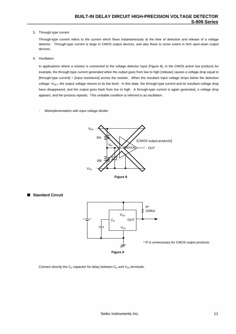
n Standard Circuit
Connect directly the CD capacitor for delay between CD and VSS terminals.
RB
RA
OUTVIN
VSS
VDD
S-809XXAL
(CMOS output products)
Figure 8
VDD
OUT
VSS
R*100kΩ
* R is unnecessary for CMOS output products.
Figure 9
CD

BUILT-IN DELAY CIRCUIT HIGH-PRECISION VOLTAGE DETECTORS-809 Series
12 Seiko Instruments Inc.
n Operation
1. Basic operation : CMOS active low output
(1) When power supply voltage VDD is greater than the release voltage +VDET, the Nch transistor is OFF and the Pch
transistor ON, causing VDD (high) to appear at the output. With the Nch transistor N1 of Figure 10 OFF, the comparator
input voltage is (RB+RC)/(RA+RB+RC×VDD.
(2) When power supply voltage VDD goes below +VDET, the output maintains the power supply voltage level, as long as VDD
remains above the detection voltage -VDET. When VDD does fall below -VDET (A in Figure 11), the Nch transistor goes ON,
the Pch transistor goes OFF, and VSS appears at the output. With the Nch transistor N 1 of Figure 10 ON, the
comparator input voltage is RB/(RA+RB)×VDD.
(3) When VDD falls below the minimum operating voltage, the output becomes undefined. However, output will revert to VDD
if a pull-up has been employed.
(4) VSS will again be output when VDD rises above the minimum operating voltage. VSS will continue to be output even when
VDD surpasses -VDET, as long as it does not exceed the release voltage +VDET.
(5) When VDD rises above +VDET (B in Figure 11), the Nch transistor goes OFF, the Pch transistor goes ON, and VDD
appears at the output. Then VDD at the OUT terminal appears with delay time(td) due to delay circuit.
2. Delay circuit
The delay circuit outputs the signal delayed from the release voltage (+VDET) point of the power voltage VDD rising.
The output signal is not delayed when the VDD goes down the detection voltage (-VDET) or less. (See Figure 11).
The delay time(td) is determined by the time constant of the built-in constant current (approx. 100nA in the case of products
with detection voltage of 1.5V or more, approx. 570nA in the case of products with detection voltage of 1.4V or less) and the
attached external capacitor (CD), and calculated from the following formula.
td (ms) = Delay factor × CD (nF)
Delay factor: (25°C)
Products with detection voltage of 1.4V or less : Min.0.57, Typ.0.77, Max.0.96
Products with detection voltage of 1.5V or more Nch open-drain outputs : Min.4.3, Typ.5.7, Max.7.2
CMOS outputs : Min.3.8, Typ.5.1, Max.6.4
AB
VDD
VSS
Release voltage (+VDET)Detection voltage (-VDET)
Min. operating voltage
OUT terminal output
Hysteresiswidth (VHYS)
VDD
VSS
(1) (2) (3) (5)(4)
Figure 10
Figure 11
+
VREF
*
Delaycircuit
CD
CD
CD
OUT
*RA
−
RB
RCN
Pch
Nch
VSS
VDD
* Parasitic diodetd

BUILT-IN DELAY DIRCUIT HIGH-PRECISION VOLTAGE DETECTOR S-809 Series
Seiko Instruments Inc. 13
[Cautions]
• The open of CD terminal may cause double pulses shown in Figure 12 at release.
If the double pulses cause a trouble, attach 10pF or larger capacitor to the CD terminal.
Do not apply the voltage to the CD terminal.
• Layout the print circuit board not to apply or flow out the current to/from the CD terminal. Doing not so may cause
inaccurate delay time..
• Use an external capacitor, CD of which leakage current can be ignored for the built-in constant-current value. A
leakage current may cause an error of delay time. Also, a leakage current over the built-in constant-current causes
unrelease status.
3. Other characteristics
(1) Temperature characteristic of detection voltage
The temperature characteristics of the detection voltage are expressed by the oblique line parts in Figure 12.
(2) Temperature characteristics of release voltage
(3) Temperature characteristics of hysteresis voltage
Samples of each temperature characteristics for (1) to (3) are shown in page 14 to page 15.
The temperature factor of the release voltage is calculated by the temperature factor of the detection
voltage as follows:
∆Ta
∆+VDET
−40 25
+0.54mV/°C
−VDET
[V]
1.500
85 Ta[°C]
-0.54mV/°C
Figure 13
S-80915AXMP:
The temperature factor of the release voltage has a same sign characteristics as the temperature factor
of the detection voltage.
∆Ta
∆−VDET
×+VDET
−VDET
=∆+VDET
∆Ta
Figure 12
Time
The temperature characteristics of hysteresis voltage is calculated as follows:
∆+VDET
∆Ta−
∆−VDET
∆Ta=
VHYS
−VDET×
∆−VDET
∆Ta
∆+VDE
∆Ta-
∆−VDET
∆Ta

BUILT-IN DELAY CIRCUIT HIGH-PRECISION VOLTAGE DETECTORS-809 Series
14 Seiko Instruments Inc.
n Characteristics (typical characteristics)
(1) Detection voltage (VDET) - Temperature (Ta)
(2) Hysteresis voltage width (Vhys) - Temperature (Ta)
Ta (°C)
Vdet(V)
Vdet(V)
(d) S-80960AN
Ta (°C)
Vdet(V)
(c) S-80915AN
20 8060400-20-40 100
6.4
6.2
6.0
+Vdet
-Vdet
Ta (°C)
20 8060400-20-40 100
1.7
1.6
1.5
+Vdet
-Vdet
Ta (°C)
Vdet(V)
5.81.4
Ta (°C)
Vhys(%)
Ta (°C)
Vhys(%)
(a) S-80911AN
20 8060400-20-40 100
+Vdet
-Vdet
1.3
1.2
1.1
1.0
(b) S-80914AN
1.6
1.5
1.4
20 8060400-20-40 100
+Vdet
-Vdet
1.3
(a) S-80911AN
20 8060400-20-40 100
8.0
7.0
6.0
5.0
4.0
3.0
(b) S-80914AN
20 8060400-20-40 100
8.0
7.0
6.0
5.0
4.0
3.0

BUILT-IN DELAY DIRCUIT HIGH-PRECISION VOLTAGE DETECTOR S-809 Series
Seiko Instruments Inc. 15
(3) Current consumption (ISS) - Input voltage (VDD)
(c) S-80915AN
20 8060400-20-40 100
8.0
Ta (°C)
7.0
6.0
5.0
4.0
3.0
(d) S-80960AN
20 8060400-20-40 100
8.0
Ta (°C)
Vhys(%)
7.0
6.0
5.0
4.0
3.0
(a) S-80911AL
VDD (V)
0 1 2 3 4
Iss
(µA)
2.5
2.0
1.5
1.0
0.5
0.0
(b) S-80914AL
(c) S-80915AL
VDD (V)
0 2 4 6 8 10
Iss
(µA)
2.5
2.0
1.5
1.0
0.5
0.012
(d) S-80960AL
VDD (V)
0 2 4 6 8 10
Iss
(µA)
2.5
2.0
1.5
1.0
0.5
0.0
Ta=25°C Ta=25°C
5 6 7 8
15µA
VDD (V)
0 1 2 3 4
Iss
(µA)
2.5
2.0
1.5
1.0
0.5
0.05 6 7 8
18µA
12.9µA3.4µA
Ta=25°C Ta=25°C
12

BUILT-IN DELAY CIRCUIT HIGH-PRECISION VOLTAGE DETECTORS-809 Series
16 Seiko Instruments Inc.
(4) Current consumption (ISS) - Temperature (Ta)
(5) Nch transistor output current (IOUT) - VDS (6) Pch transistor output current (IOUT) - VDS
Ta (°C)
Iss (µA)
Ta (°C)
Iss (µA)
(c) S-80915AN
20 8060400-20-40 100
2.0
Ta (°C)
Iss (µA)
1.5
1.0
0.5
0.0
(d) S-80960AN
20 8060400-20-40 100
2.0
Ta (°C)
Iss (µA)
1.5
1.0
0.5
0.0
VDD=3.5V VDD=7.5V
(a) S-80960AL
10
(a) S-80960AL
VDS (V)
60
50
40
30
20
10
00 1 2 3 4 5
VDD=6.0 V
VDD=4.8 V
VDD=3.6 V
VDD=2.4 V
VDD=1.2V
(a) S-80915AL
VDS (V)
30
25
20
15
10
5
00 2 4 6 8
IOUT
(mA)
VDD=8.4 V
VDD=7.2 V
VDD=6.0 V
VDD=4.8 V
VDD=3.6 V
VDD=2.4 V
Ta=25°C Ta=25°C
(a) S-80911AN
20 8060400-20-40 100
2.0
1.5
1.0
0.5
0.0
VDD=2.0V(b) S-80914AN
20 860400-20-40 100
2.0
1.5
1.0
0.5
0.0
VDD=2.0V
IOUT
(mA)

BUILT-IN DELAY DIRCUIT HIGH-PRECISION VOLTAGE DETECTOR S-809 Series
Seiko Instruments Inc. 17
(7) Nch transistor output current (IOUT) - Input voltage(VDD)
(8) Pch transistor output current(IOUT) - Input voltage(VDD)
(9) Minimum operating voltage
VDS =0.5V5.0
4.0
3.0
2.0
1.0
0.00 2 4 6 8 10 12
Ta=−40°C
Ta=25°C
Ta=85°C
(b) S-80915AL
VDD (V)
IOUT
(mA)
VDD =0.5V(b) S-80960AL
20
15
10
5
00 2 4 6 8
IOUT
(mA)
Ta=−40°C
Ta=25°C
Ta=85°C
VDD (V)
VOUT
(V)1.0
(b) S-80915AN(PULL- UP VDD : 100KΩ)
0.0
0.0
VDD (V)
0.5
1.5
0.5 1.0 1.5 2.0
2.0
Ta=-40°C
Ta =25°C
Ta=85°C
2.5
VDD (V)
VDS =0.5V(a) S -80914AL
00
0.5
1
2
3
0.5 1 21.5
3.5
2.5
1.5
IOUT
(mA)
Ta=−40°C
Ta=25°C
Ta=85°C
Ta=−40°C
VDD (V)
Ta=85°C
Ta=25°C
(a) S-80911AL
0 1.0 2 2.5 30
0.5
1
2
3
2.5
1.5
IOUT
(mA)
VDS =0.5V
1.5
VOUT
(V)1.0
(a) S-80911AN(PULL- UP VDD : 100KΩ)
0.0
0.0
VDD (V)
0.5
1.5
0.5 1.0 1.5 2.0
2.0
Ta=−40°C
Ta =25°C
Ta=85°C
2.5

BUILT-IN DELAY CIRCUIT HIGH-PRECISION VOLTAGE DETECTORS-809 Series
18 Seiko Instruments Inc.
(10) Dynamic response (CD : Open)
Load capacitance (µF) Load capacitance (µF)
Load capacitance (µF)
Responsetime(ms)
Responsetime(ms)
Responsetime(ms)
Responsetime(ms)
Responsetime(ms)
Responsetime(ms)
Load capacitance(µF)
0.1
(e) S-80915AL
0.0001 0.001 0.01 0.1
0.001
1
0.01
0.1
tPLH
tPHL
Load capacitance (µF)
(f) S-80915AN
0.0001 0.001 0.01
0.01
10
0.1
1
tPLH
tPHL
Load capacitance (µF)
Ta=25°C Ta=25°C
(a) S-80911AL
0.0001 0.001 0.01 0.1
0.001
1
0.01
0.1
tPLH
tPHL
Ta=25°C(b) S-80911AN
0.0001 0.001 0.01 0.1
tPLH
tPHL
0.01
10
0.1
1
Ta=25°C
(c) S-80914AL
0.0001 0.001 0.01 0.1
0.001
1
0.01
0.1
tPLH
tPHL
Ta=25°C(d) S-80914AN
0.0001 0.001 0.01
0.01
10
0.1
1
tPLH
tPHL
Ta=25°C

BUILT-IN DELAY DIRCUIT HIGH-PRECISION VOLTAGE DETECTOR S-809 Series
Seiko Instruments Inc. 19
(11) Delay time (td) - External capacitor(CD)
VDD OU
VS
Input Voltage
Output Voltage
VDD
S-809
SeriesV
Responsetime(ms)
Responsetime(ms)
(h) S-80960AN
0.0001
V
0.001 0.01 0.1
R*100KΩ
tPLH
tPHL
Load capacitance (µF)
0.01
10
0.1
1
(g) S-80960AL
0.0001 0.001 0.01 0.1
0.001
1
0.01
0.1
tPLH
tPHL
Load capacitance (µF)
Ta=25°C Ta=25°C
(a) S-80911AN
*’R’ is not needed for CMOS output products.
Figure 14 Measuring conditions of response time
Figure 15 Measuring circuit of response time
(a)to(d) : VIH=6V, VIL=0.80V
(e)to(h) : VIH=10V, VIL=0.95V
VDD×90 %
VDD×10 %
VIH
VIL
VDD
tPHL tPLH
1µsec1µsec
CD (nF)
1000
1
10
100
0.1
0.010.1 1 10 100
td (ms)
10000.01
Ta=25°C

BUILT-IN DELAY CIRCUIT HIGH-PRECISION VOLTAGE DETECTORS-809 Series
20 Seiko Instruments Inc.
(12) Delay time (tpd) - Temperature (Ta)
(b) S-80915AN
10000
10
100
1000
1
0.10.1 1 10 100
CD (nF)
td (ms)
10000.01
(a) S-80911AN
Ta (°C)
td (ms)
Ta=25°C
(b) S-80915AN
20 8060400-20-40 100
50
Ta (°C)
td (ms)
40
30
20
10
0
CD =4.7nF
20 8060400-20-40 100
10
8
6
4
2
0
CD =4.7nF
9
7
5
3
1
VDD
CD
OUT
VSS
VDD
S-809
SeriesV
V
R100KΩ
VDD×90 %
VSS
VIH
VILtd
1µsec
Figure 16 Measuring conditions of delay timeFigure 17 Measuring circuit of delay time
(a) : VIH=6V, VIL=0.80V
(b) : VIH=10V, VIL=0.95V
Input Voltage
Output Voltage

BUILT-IN DELAY DIRCUIT HIGH-PRECISION VOLTAGE DETECTOR S-809 Series
Seiko Instruments Inc. 21
n Application Circuit Examples
1. Microcomputer reset circuits
With the S-809 Series which has a low operating voltage, a high-precision detection voltage and hysteresis characteristic, the
reset circuits shown in Figures 18 to 19 can be easily constructed.
2. Change of detection voltege
In Nch open-drain output products of the S-809 Series, detection voltage can be changed using resistance dividers or diodes
as shown in Figures 20 and 21. In Figure 20, hysteresis width is also changed.
n Notes
In CMOS output products of the S-809 Series, through type current flows when the device is detecting or releasing. If a high
impedance is connected to the input, oscillation may be caused due to the fall of the voltage by the through type current when
lowering the voltage during releasing.
When designing for mass production using an application circuit described herein, take the product deviation and temperature
characteristic into consideration.
Seiko Instruments Inc. shall not bear any responsibility for the patents on the circuits described herein.
VSS
VSS
VDD
Micro-computer
S-809XXAL
Figure 18(Nch open-drain output products only)
VDD1 VDD2
Micro-computer
S-809XXAN
Figure 19
RA≤75kΩ
RA
OUTVIN
VSS
VDD
Note1: If RA and RB are large, the hysteresis width may belarger than the value given by the formula above dueto through type current (which flows slightly in Nchopen-drain circuit).
Note2: RA should be 75kΩor less to prevent oscilation.
+
−
S-809XXAN
Figure 20
R
Vf1
(Nch open-drain products)
(Nch open-drain products)
OUTVIN
VSS
VDD
S-809XXAN
Vf2
Detection voltage = −VDETRA+RB
RB
Hysteresis width = VHYSRA+RB
RBFigure 21
Detection voltage =Vf1+Vf2+ (−VDET)

3.25±0.15
ø1.5 +0.1 -0
ø1.0 +0.1 -0 4.0±0.1
2.0±0.050.27±0.05
1.4±0.2
Feed direction
SOT-23-5 MP005-A 991105
0.95 0.1
2.9±0.2
+0.1 -0.060.16
1.9±0.2
0.4±0.1
1 2 3
45
21±0.5
2±0.2
(60°)(60°)
φ13±0.2
12.5max.
9.0±0.3
+0.2 -0.32.81.6
1.1±0.1
0.45
1.3max
3 max.
3 max.
4.0±0.1 (10 pitches 40.0±0.2)
Taping Specifications Reel Specifications
Dimensions Unit mm
3000 pcs./reel

Markings990603809/816/8520
SOT-23-5
4
1 3
5

• The information herein is subject to change without notice.
• Seiko Instruments Inc. is not responsible for any problems caused by circuits or other diagrams
described herein whose industrial properties, patents or other rights belong to third parties. The
application circuit examples explain typical applications of the products, and do not guarantee any
mass-production design.
• When the products described herein include Strategic Products (or Service) subject to regulations,
they should not be exported without authorization from the appropriate governmental authorities.
• The products described herein cannot be used as part of any device or equipment which influences
the human body, such as physical exercise equipment, medical equipment, security system, gas
equipment, vehicle or airplane, without prior written permission of Seiko Instruments Inc.
Recommended

![APPLICATION OF TIME DELAY VALVES - idc-online.com...APPLICATION OF TIME DELAY VALVES Figure 6.8 Time Delay Valve Circuit [N.C] Ex.: 1 Use of Pressure Sequence Valve in Clamping Application](https://img.pdfslide.net/doc/110x75/609c27d0c3052d446773a78d/application-of-time-delay-valves-idc-application-of-time-delay-valves-figure.jpg)