1
Introduction To Materials Science FOR ENGINEERS, Ch. 19
University of Tennessee, Dept. of Materials Science and Engineering1
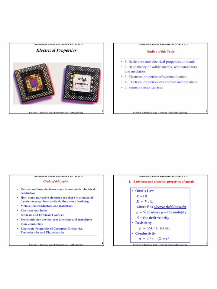
Electrical Properties
Introduction To Materials Science FOR ENGINEERS, Ch. 19
University of Tennessee, Dept. of Materials Science and Engineering2
Goals of this topic:
• Understand how electrons move in materials: electrical conduction
• How many moveable electrons are there in a material (carrier density), how easily do they move (mobility)
• Metals, semiconductors and insulators• Electrons and holes• Intrinsic and Extrinsic Carriers• Semiconductor devices: p-n junctions and transistors• Ionic conduction• Electronic Properties of Ceramics: Dielectrics,
Ferroelectrics and Piezoelectrics
Introduction To Materials Science FOR ENGINEERS, Ch. 19
University of Tennessee, Dept. of Materials Science and Engineering3
Outline of this Topic
• 1. Basic laws and electrical properties of metals• 2. Band theory of solids: metals, semiconductors
and insulators• 3. Electrical properties of semiconductors• 4. Electrical properties of ceramics and polymers• 5. Semiconductor devices
Introduction To Materials Science FOR ENGINEERS, Ch. 19
University of Tennessee, Dept. of Materials Science and Engineering4
• Ohm’s LawV = IRE = V / Lwhere E is electric field intensityµ = / E where µ = the mobility
• Resistivityρ = RA / L (Ω.m)
• Conductivityσ = 1 / ρ (Ω.m)-1
ν
ν = the drift velocity
1. Basic laws and electrical properties of metals
2
Introduction To Materials Science FOR ENGINEERS, Ch. 19
University of Tennessee, Dept. of Materials Science and Engineering5
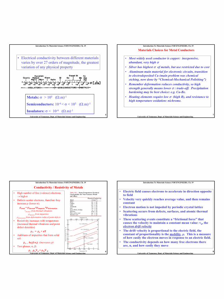
• Electrical conductivity between different materials varies by over 27 orders of magnitude, the greatest variation of any physical property
Metals: σ > 105 (Ω.m)-1
Semiconductors: 10-6 < σ < 105 (Ω.m)-1
Insulators: σ < 10-6 (Ω.m)-1
Introduction To Materials Science FOR ENGINEERS, Ch. 19
University of Tennessee, Dept. of Materials Science and Engineering6
Conductivity / Resistivity of Metals
• High number of free (valence) electrons → high σ
• Defects scatter electrons, therefore they increase ρ (lower σ). ρtotal = ρthermal+ρimpurity+ρdeformation
ρthermal from thermal vibrations
ρimpurity from impuritiesρdeformation from deformation-induced point defects
• Resistivity increases with temperature (increased thermal vibrations and point defect densities)
ρT = ρo + aT• Additions of impurities that form solid
sol:ρI = Aci(1-ci) (increases ρ)
• Two phases, α, β:ρi = ραVα + ρ βV β
Introduction To Materials Science FOR ENGINEERS, Ch. 19
University of Tennessee, Dept. of Materials Science and Engineering7
Materials Choices for Metal Conductors
• Most widely used conductor is copper: inexpensive, abundant, very high σ
• Silver has highest σ of metals, but use restricted due to cost• Aluminum main material for electronic circuits, transition
to electrodeposited Cu (main problem was chemical etching, now done by “Chemical-Mechanical Polishing”)
• Remember deformation reduces conductivity, so high strength generally means lower σ : trade-off. Precipitation hardening may be best choice: e.g. Cu-Be.
• Heating elements require low σ (high R), and resistance to high temperature oxidation: nichrome.
Introduction To Materials Science FOR ENGINEERS, Ch. 19
University of Tennessee, Dept. of Materials Science and Engineering8
• Electric field causes electrons to accelerate in direction opposite to field
• Velocity very quickly reaches average value, and then remains constant
• Electron motion is not impeded by periodic crystal lattice• Scattering occurs from defects, surfaces, and atomic thermal
vibrations• These scattering events constitute a “frictional force” that
causes the velocity to maintain a constant mean value: vd, the electron drift velocity
• The drift velocity is proportional to the electric field, the constant of proportionality is the mobility, µ. This is a measure of how easily the electron moves in response to an electric field.
• The conductivity depends on how many free electrons there are, n, and how easily they move
3
Introduction To Materials Science FOR ENGINEERS, Ch. 19
University of Tennessee, Dept. of Materials Science and Engineering9
vd = µeE
σ = n|e| µen : number of “free” or conduction electrons per
unit volume
EScattering events
Net electron motion
Introduction To Materials Science FOR ENGINEERS, Ch. 19
University of Tennessee, Dept. of Materials Science and Engineering10
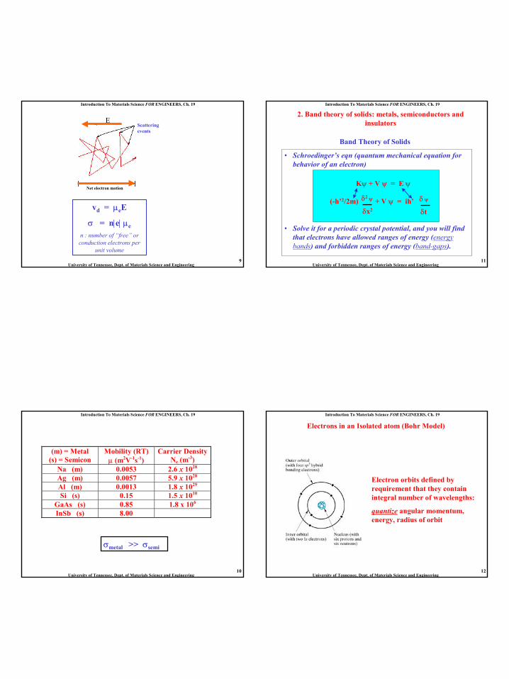
(m) = Metal (s) = Semicon
Mobility (RT) µ (m2V-1s-1)
Carrier DensityNe (m-3)
Na (m) 0.0053 2.6 x 1028
Ag (m) 0.0057 5.9 x 1028 Al (m) 0.0013 1.8 x 1029 Si (s) 0.15 1.5 x 10¹⁰
GaAs (s) 0.85 1.8 x 10⁶
InSb (s) 8.00
σmetal >> σsemi
Introduction To Materials Science FOR ENGINEERS, Ch. 19
University of Tennessee, Dept. of Materials Science and Engineering11
Band Theory of Solids
• Schroedinger’s eqn (quantum mechanical equation for behavior of an electron)
• Solve it for a periodic crystal potential, and you will find that electrons have allowed ranges of energy (energy bands) and forbidden ranges of energy (band-gaps).
δ2 ψ
δx2
δ ψ
δt
Kψ + V ψ = E ψ
(-h’2/2m) + V ψ = ih’
2. Band theory of solids: metals, semiconductors and insulators
Introduction To Materials Science FOR ENGINEERS, Ch. 19
University of Tennessee, Dept. of Materials Science and Engineering12
Electrons in an Isolated atom (Bohr Model)
Electron orbits defined by requirement that they contain integral number of wavelengths:
quantize angular momentum, energy, radius of orbit
4
Introduction To Materials Science FOR ENGINEERS, Ch. 19
University of Tennessee, Dept. of Materials Science and Engineering13
• When N atoms in a solid are relatively far apart, they do not interact, so electrons in a given shell in different atoms have same energy
• As atoms come closer together, they interact, perturbing electron energy levels
• Electrons from each atom then have slightly different energies, producing a “band” of allowed energies
Introduction To Materials Science FOR ENGINEERS, Ch. 19
University of Tennessee, Dept. of Materials Science and Engineering14
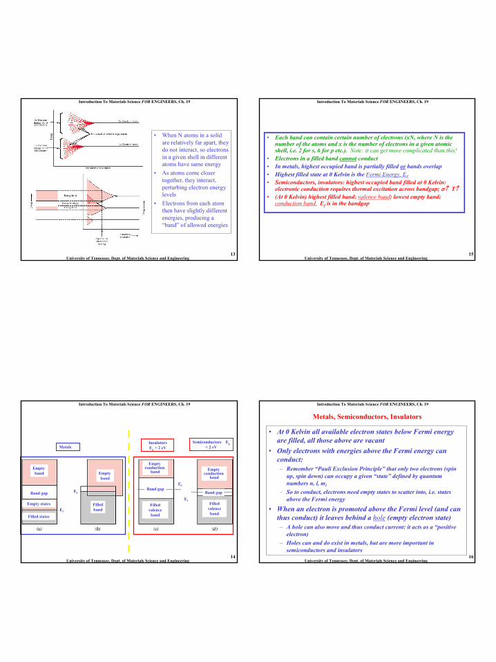
MetalsSemiconductors Eg
< 2 eVInsulators Eg > 2 eV
Empty band
Empty conduction
bandEmpty band
Band gap
Empty states
Filled states
Filledband
Filled valenceband
Empty conduction
band
Ef
Ef
Ef
Ef
Band gapBand gap
Filled valenceband
Introduction To Materials Science FOR ENGINEERS, Ch. 19
University of Tennessee, Dept. of Materials Science and Engineering15
• Each band can contain certain number of electrons (xN, where N is the number of the atoms and x is the number of electrons in a given atomic shell, i.e. 2 for s, 6 for p etc.). Note: it can get more complicated than this!
• Electrons in a filled band cannot conduct• In metals, highest occupied band is partially filled or bands overlap• Highest filled state at 0 Kelvin is the Fermi Energy, EF• Semiconductors, insulators: highest occupied band filled at 0 Kelvin:
electronic conduction requires thermal excitation across bandgap; σ↑ T↑• (At 0 Kelvin) highest filled band: valence band; lowest empty band:
conduction band. Ef is in the bandgap
Introduction To Materials Science FOR ENGINEERS, Ch. 19
University of Tennessee, Dept. of Materials Science and Engineering16
Metals, Semiconductors, Insulators
• At 0 Kelvin all available electron states below Fermi energy are filled, all those above are vacant
• Only electrons with energies above the Fermi energy can conduct:– Remember “Pauli Exclusion Principle” that only two electrons (spin
up, spin down) can occupy a given “state” defined by quantum numbers n, l, ml
– So to conduct, electrons need empty states to scatter into, i.e. states above the Fermi energy
• When an electron is promoted above the Fermi level (and can thus conduct) it leaves behind a hole (empty electron state)– A hole can also move and thus conduct current: it acts as a “positive
electron)– Holes can and do exist in metals, but are more important in
semiconductors and insulators
5
Introduction To Materials Science FOR ENGINEERS, Ch. 19
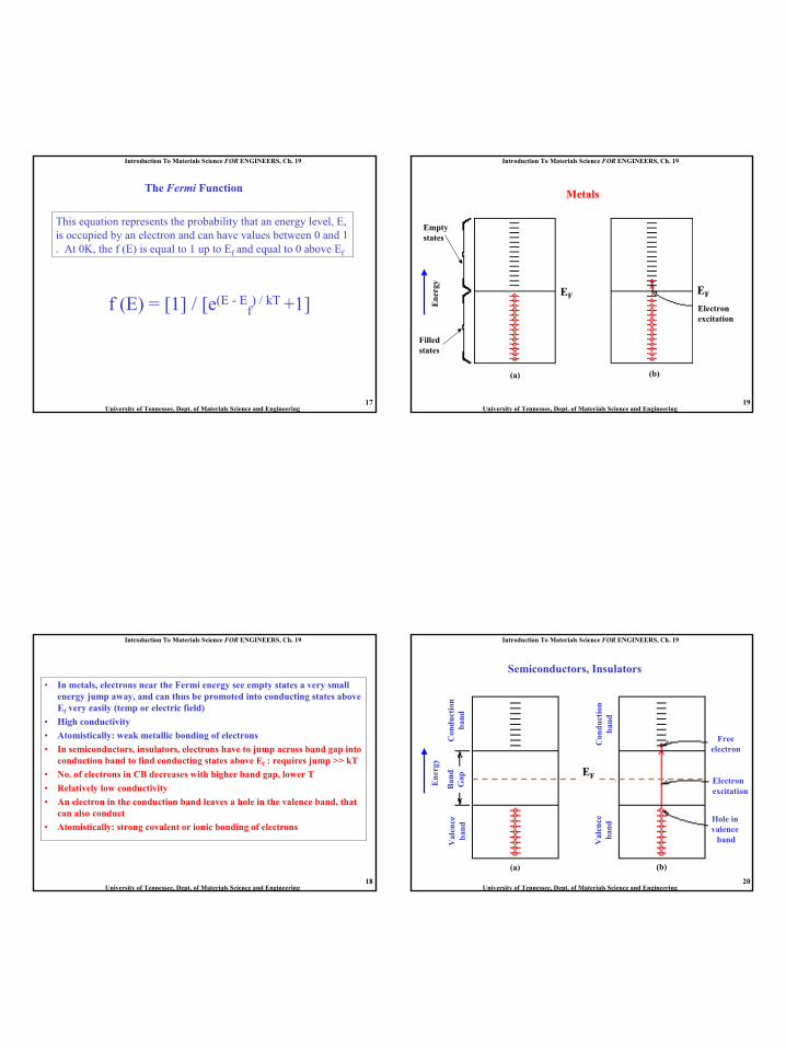
University of Tennessee, Dept. of Materials Science and Engineering17
The Fermi Function
f (E) = [1] / [e(E - Ef) / kT +1]
This equation represents the probability that an energy level, E, is occupied by an electron and can have values between 0 and 1. At 0K, the f (E) is equal to 1 up to Ef and equal to 0 above Ef
Introduction To Materials Science FOR ENGINEERS, Ch. 19
University of Tennessee, Dept. of Materials Science and Engineering18
• In metals, electrons near the Fermi energy see empty states a very small energy jump away, and can thus be promoted into conducting states above Ef very easily (temp or electric field)
• High conductivity• Atomistically: weak metallic bonding of electrons• In semiconductors, insulators, electrons have to jump across band gap into
conduction band to find conducting states above Ef : requires jump >> kT• No. of electrons in CB decreases with higher band gap, lower T• Relatively low conductivity• An electron in the conduction band leaves a hole in the valence band, that
can also conduct• Atomistically: strong covalent or ionic bonding of electrons
Introduction To Materials Science FOR ENGINEERS, Ch. 19
University of Tennessee, Dept. of Materials Science and Engineering19
Metals
Empty states
Filled states
(b)(a)
EF
Ene
rgy
Electronexcitation
EF
Introduction To Materials Science FOR ENGINEERS, Ch. 19
University of Tennessee, Dept. of Materials Science and Engineering20
Semiconductors, Insulators
Val
ence
band
Con
duct
ion
band
Ban
dG
ap
Val
ence
band
Con
duct
ion
band
(b)(a)
Electronexcitation
Freeelectron
Hole in valence
band
Ene
rgy
EF
6
Introduction To Materials Science FOR ENGINEERS, Ch. 19
University of Tennessee, Dept. of Materials Science and Engineering21
Electrical conduction in intrinsic Si, (a) before excitation, (b) and (c) after excitation, see the response of the electron-hole pairs to the external field. Note: holes generally have lower mobilities than electrons in a given material (require cooperative motion of electrons into previous hole sites)
E field
Si Si Si Si
Si Si Si Si
Si Si Si Si
Si Si Si Si
Si Si Si Si
Si Si Si Si
hole
free electron
E field
Si Si Si Si
Si Si Si Si
Si Si Si Si
hole
free electron
(b)(a)
Introduction To Materials Science FOR ENGINEERS, Ch. 19
University of Tennessee, Dept. of Materials Science and Engineering22
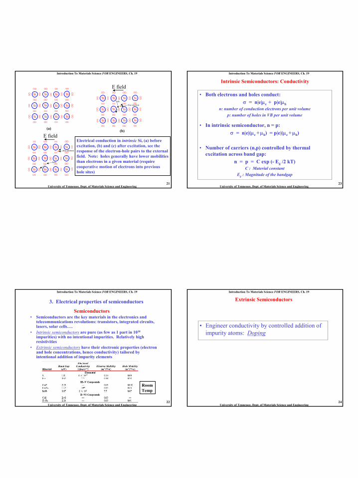
Semiconductors• Semiconductors are the key materials in the electronics and
telecommunications revolutions: transistors, integrated circuits, lasers, solar cells….
• Intrinsic semiconductors are pure (as few as 1 part in 1010
impurities) with no intentional impurities. Relatively high resistivities
• Extrinsic semiconductors have their electronic properties (electron and hole concentrations, hence conductivity) tailored by intentional addition of impurity elements
Room Temp
3. Electrical properties of semiconductors
Introduction To Materials Science FOR ENGINEERS, Ch. 19
University of Tennessee, Dept. of Materials Science and Engineering23
Intrinsic Semiconductors: Conductivity
• Both electrons and holes conduct:σ = n|e|µe + p|e|µh
n: number of conduction electrons per unit volumep: number of holes in VB per unit volume
• In intrinsic semiconductor, n = p:σ = n|e|(µe +µh) = p|e|(µe +µh)
• Number of carriers (n,p) controlled by thermal excitation across band gap:
n = p = C exp (- Eg /2 kT)C : Material constant
Eg : Magnitude of the bandgap
Introduction To Materials Science FOR ENGINEERS, Ch. 19
University of Tennessee, Dept. of Materials Science and Engineering24
Extrinsic Semiconductors
• Engineer conductivity by controlled addition of impurity atoms: Doping
7
Introduction To Materials Science FOR ENGINEERS, Ch. 19
University of Tennessee, Dept. of Materials Science and Engineering25
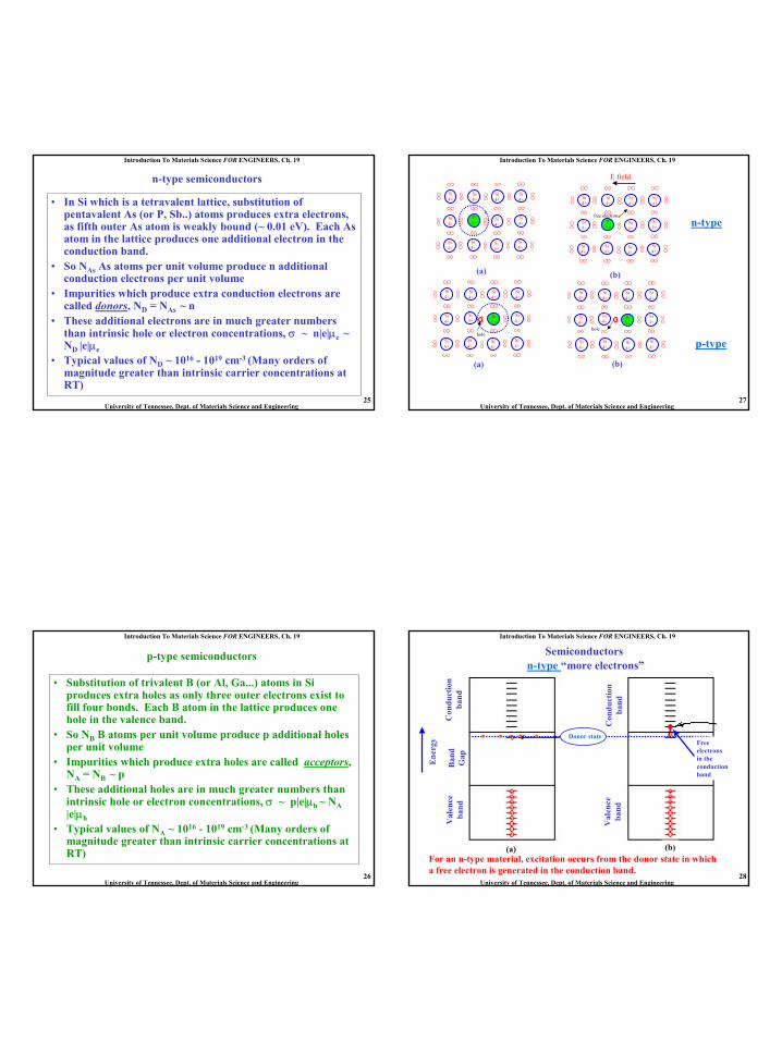
n-type semiconductors
• In Si which is a tetravalent lattice, substitution of pentavalent As (or P, Sb..) atoms produces extra electrons, as fifth outer As atom is weakly bound (~ 0.01 eV). Each As atom in the lattice produces one additional electron in the conduction band.
• So NAs As atoms per unit volume produce n additional conduction electrons per unit volume
• Impurities which produce extra conduction electrons are called donors, ND = NAs ~ n
• These additional electrons are in much greater numbers than intrinsic hole or electron concentrations, σ ~ n|e|µe ~ ND |e|µe
• Typical values of ND ~ 1016 - 1019 cm-3 (Many orders of magnitude greater than intrinsic carrier concentrations at RT)
Introduction To Materials Science FOR ENGINEERS, Ch. 19
University of Tennessee, Dept. of Materials Science and Engineering26
p-type semiconductors
• Substitution of trivalent B (or Al, Ga...) atoms in Si produces extra holes as only three outer electrons exist to fill four bonds. Each B atom in the lattice produces one hole in the valence band.
• So NB B atoms per unit volume produce p additional holes per unit volume
• Impurities which produce extra holes are called acceptors, NA = NB ~ p
• These additional holes are in much greater numbers than intrinsic hole or electron concentrations, σ ~ p|e|µh ~ NA |e|µh
• Typical values of NA ~ 1016 - 1019 cm-3 (Many orders of magnitude greater than intrinsic carrier concentrations at RT)
Introduction To Materials Science FOR ENGINEERS, Ch. 19
University of Tennessee, Dept. of Materials Science and Engineering27
n-type
p-type
Si4+
(a)
Si4+
Si4+
Si4+
Si4+
Si4+
Si4+
P5+
Si4+
Si4+
Si4+
Si4+
Si4+
(a)
Si4+
Si4+
Si4+
Si4+
Si4+
B3+
Si4+
holeSi4+
Si4+
Si4+
Si4+
(b)
Si4+
Si4+
Si4+
Si4+
Si4+
Si4+
B3+
Si4+
hole
Si4+
Si4+
Si4+
Si4+
Si4+
(b)
Si4+
Si4+
Si4+
Si4+
Si4+
Si4+
P5+
E field
free electron
Si4+
Si4+
Si4+
Si4+
Introduction To Materials Science FOR ENGINEERS, Ch. 19
University of Tennessee, Dept. of Materials Science and Engineering28
Semiconductors
Val
ence
band
Con
duct
ion
band
Ban
dG
ap
Val
ence
band
Con
duct
ion
band
(b)(a)
Ene
rgy Donor state
n-type “more electrons”
Freeelectrons in the conduction band
For an n-type material, excitation occurs from the donor state in which a free electron is generated in the conduction band.
8
Introduction To Materials Science FOR ENGINEERS, Ch. 19
University of Tennessee, Dept. of Materials Science and Engineering29
Semiconductors
Val
ence
band
Con
duct
ion
band
Ban
dG
ap
Val
ence
band
Con
duct
ion
band
(b)(a)
Ene
rgy
p-type “more holes”
Hole in the valenceband
Acceptor state
For an p-type material, excitation of an electron into the acceptor level, leaving behind a hole in the valence band.
Introduction To Materials Science FOR ENGINEERS, Ch. 19
University of Tennessee, Dept. of Materials Science and Engineering30
Temperature Dependence of carrier Concentration and Conductivity
• Our basic equation:σ = n|e|µe + p|e|µh
• Main temperature variations are in n,p rather than µe ,µh
• Intrinsic carrier concentrationn = p = C exp (- Eg /2 kT)
Extrinsic carrier concentration– low T (< room temp) Extrinsic
regime: ionization of dopants– mid T (inc. room temp) Saturated
regime: most dopants ionized– high T Intrinsic regime: intrinsic
generation dominates
Saturation
Intrinsic
1/T
Extrinsic
ln p
, n
∆ln p/ [∆(1/T)]
= Eg / 2 k
Introduction To Materials Science FOR ENGINEERS, Ch. 19
University of Tennessee, Dept. of Materials Science and Engineering31
4. Electrical properties of ceramics and polymers
Introduction To Materials Science FOR ENGINEERS, Ch. 19
University of Tennessee, Dept. of Materials Science and Engineering32
Dielectric Materials
• A dielectric material is an insulator which contains electric dipoles, that is where positive and negative charge are separated on an atomic or molecular level
• When an electric field is applied, these dipoles align to the field, causing a net dipole moment that affects the material properties.
9
Introduction To Materials Science FOR ENGINEERS, Ch. 19
University of Tennessee, Dept. of Materials Science and Engineering33
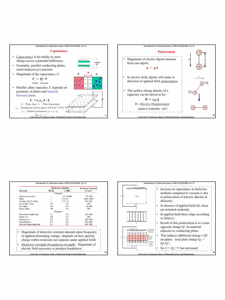
Capacitance
• Capacitance is the ability to store charge across a potential difference.
• Examples: parallel conducting plates, semiconductor p-n junction
• Magnitude of the capacitance, C:C = Q / VUnits: Farads
• Parallel- plate capacitor, C depends on geometry of plates and material between plates
C = εr εo A / LA : Plate Area; L : Plate Separation
ε o : Permittivity of Free Space (8.85x10⁻¹² F/m2)ε r : Relative permittivity, εr = ε /εo
Vac, εr = 1
+ + + + +
- - - - - -
P N
+++
++++++
--
--
-
---
-
D
L
Introduction To Materials Science FOR ENGINEERS, Ch. 19
University of Tennessee, Dept. of Materials Science and Engineering34
• Magnitude of dielectric constant depends upon frequency of applied alternating voltage (depends on how quickly charge within molecule can separate under applied field)
• Dielectric strength (breakdown strength): Magnitude of electric field necessary to produce breakdown
Introduction To Materials Science FOR ENGINEERS, Ch. 19
University of Tennessee, Dept. of Materials Science and Engineering35
Polarization
• Magnitude of electric dipole moment from one dipole:
p = q d
• In electric field, dipole will rotate in direction of applied field: polarization
• The surface charge density of a capacitor can be shown to be:
D = εoεrξD : Electric Displacement
(units Coulombs / m2)
Introduction To Materials Science FOR ENGINEERS, Ch. 19
University of Tennessee, Dept. of Materials Science and Engineering36
• Increase in capacitance in dielectric medium compared to vacuum is due to polarization of electric dipoles in dielectric.
• In absence of applied field (b), these are oriented randomly
• In applied field these align according to field (c)
• Result of this polarization is to create opposite charge Q’ on material adjacent to conducting plates
• This induces additional charge (-)Q’ on plates: total plate charge Qt = |Q+Q’|.
• So, C = Qt / V has increased
10
Introduction To Materials Science FOR ENGINEERS, Ch. 19
University of Tennessee, Dept. of Materials Science and Engineering37
• Surface density charge now D = εξ = εoεrξ = εoξ + P
• P is the polarization of the material (units Coulombs/m2). It represents the total electric dipole moment per unit volume of dielectric, or the polarization electric field arising from alignment of electric dipoles in the dielectric
• From equations at top of pageP = εo(εr-1)ξ
Introduction To Materials Science FOR ENGINEERS, Ch. 19
University of Tennessee, Dept. of Materials Science and Engineering38
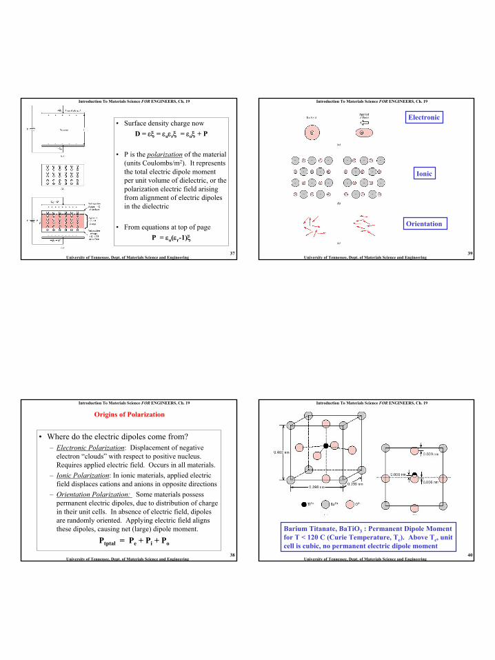
Origins of Polarization
• Where do the electric dipoles come from?– Electronic Polarization: Displacement of negative
electron “clouds” with respect to positive nucleus. Requires applied electric field. Occurs in all materials.
– Ionic Polarization: In ionic materials, applied electric field displaces cations and anions in opposite directions
– Orientation Polarization: Some materials possess permanent electric dipoles, due to distribution of charge in their unit cells. In absence of electric field, dipoles are randomly oriented. Applying electric field aligns these dipoles, causing net (large) dipole moment.
Ptptal = Pe + Pi + Po
Introduction To Materials Science FOR ENGINEERS, Ch. 19
University of Tennessee, Dept. of Materials Science and Engineering39
Electronic
Ionic
Orientation
Introduction To Materials Science FOR ENGINEERS, Ch. 19
University of Tennessee, Dept. of Materials Science and Engineering40
Barium Titanate, BaTiO3 : Permanent Dipole Moment for T < 120 C (Curie Temperature, Tc). Above Tc, unit cell is cubic, no permanent electric dipole moment
11
Introduction To Materials Science FOR ENGINEERS, Ch. 19
University of Tennessee, Dept. of Materials Science and Engineering41
Piezoelectricity
• In some ceramic materials, application of external forces produces an electric (polarization) field and vice-versa
• Applications of piezoelectric materials microphones, strain gauges, sonar detectors
• Materials include barium titanate, lead titanate, lead zirconate
Introduction To Materials Science FOR ENGINEERS, Ch. 19
University of Tennessee, Dept. of Materials Science and Engineering42
Ionic Conduction in Ceramics
• Cations and anions possess electric charge (+,-) and therefore can also conduct a current if they move.
• Ionic conduction in a ceramic is much less easy than electron conduction in a metal (“free” electrons can move far more easily than atoms / ions)
• In ceramics, which are generally insulators and have very few free electrons, ionic conduction can be a significant component of the total conductivity
σtotal = σelectronic + σionic
• Overall conductivities, however, remain very low in ceramics.
Introduction To Materials Science FOR ENGINEERS, Ch. 19
University of Tennessee, Dept. of Materials Science and Engineering43
Introduction To Materials Science FOR ENGINEERS, Ch. 19
University of Tennessee, Dept. of Materials Science and Engineering44
Electrical Properties of Polymers
• Most polymeric materials are relatively poor conductors of electrical current - low number of free electrons
• A few polymers have very high electrical conductivity - about one quarter that of copper, or about twice that of copper per unit weight.
• Involves doping with electrically active impurities, similar to semiconductors: both p- and n-type
• Examples: polyacetylene, polyparaphenylene, polypyrrole• Orienting the polymer chains (mechanically, or magnetically) during
synthesis results in high conductivity along oriented direction• Applications: advanced battery electrodes, antistatic coatings,
electronic devices• Polymeric light emitting diodes are also becoming a very important
research field
12
Introduction To Materials Science FOR ENGINEERS, Ch. 19
University of Tennessee, Dept. of Materials Science and Engineering45
5. Semiconductor Devices and Circuits
Introduction To Materials Science FOR ENGINEERS, Ch. 19
University of Tennessee, Dept. of Materials Science and Engineering46
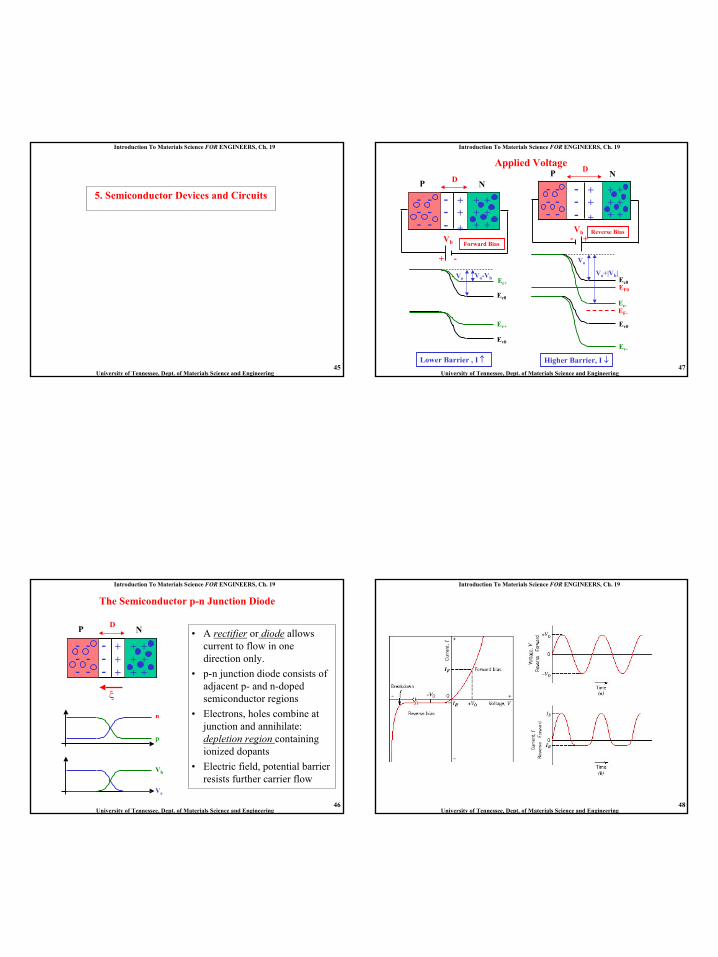
The Semiconductor p-n Junction Diode
• A rectifier or diode allows current to flow in one direction only.
• p-n junction diode consists of adjacent p- and n-doped semiconductor regions
• Electrons, holes combine at junction and annihilate: depletion region containing ionized dopants
• Electric field, potential barrier resists further carrier flow
P N
+++
++++++
--
--
-
---
-
D
p
n
Vh
Ve
ξ
Introduction To Materials Science FOR ENGINEERS, Ch. 19
University of Tennessee, Dept. of Materials Science and Engineering47
Applied Voltage
P N
+++
++++++
--
--
-
---
-
D
+ -
Forward BiasVb
Ev0
Ec0
Vo Ec+
Ev+
Vo-Vb
Lower Barrier , I ↑ Higher Barrier, I ↓
P N
+++
---
--
---
- ++++++
D
+-Reverse BiasVb
EF0
Ev0
Ec0
Vo
Ec-
Ev-
EF-
Vo+|Vb|
Introduction To Materials Science FOR ENGINEERS, Ch. 19
University of Tennessee, Dept. of Materials Science and Engineering48
13
Introduction To Materials Science FOR ENGINEERS, Ch. 19
University of Tennessee, Dept. of Materials Science and Engineering49
Transistors
• The basic building block of the microelectronic revolution• Can be made as small as 1 square micron• A single 8” diameter wafer of silicon can contain as many as
1010 - 1011 transistors in total: enough for several for every man, woman, and child on the planet
• Cost to consumer ~ 0.00001c each.• Achieved through sub-micron engineering of semiconductors,
metals, insulators and polymers.• Requires ~ $2 billion for a state-of-the-art fabrication facility
Introduction To Materials Science FOR ENGINEERS, Ch. 19
University of Tennessee, Dept. of Materials Science and Engineering50
Bipolar Junction Transistor
• n-p-n or p-n-p sandwich structures. Emitter-base-collector. Base is very thin (~ 1 micron or less) but greater than depletion region widths at p-n junctions.
• Emitter-base junction is forward biased; holes are pushed across junction. Some of these recombine with electrons in the base, but most cross the base as it so thin. They are then swept into the collector.
• A small change in base-emitter voltage causes a relatively large change in emitter-base-collector current, and hence a large voltage change across output (“load”) resistor: voltage amplification
• The above configuration is called the “common base” configuration (base is common to both input and output circuits). The “common emitter” configuration can produce both amplification (V,I) and very fast switching
Introduction To Materials Science FOR ENGINEERS, Ch. 19
University of Tennessee, Dept. of Materials Science and Engineering51
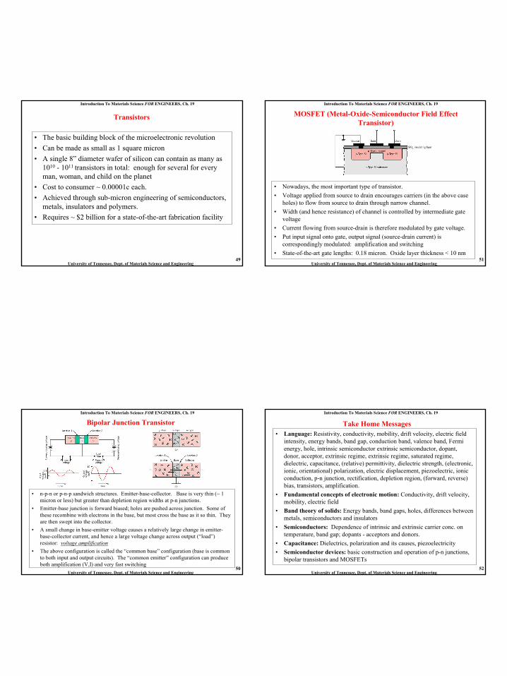
MOSFET (Metal-Oxide-Semiconductor Field Effect Transistor)
• Nowadays, the most important type of transistor.• Voltage applied from source to drain encourages carriers (in the above case
holes) to flow from source to drain through narrow channel.• Width (and hence resistance) of channel is controlled by intermediate gate
voltage• Current flowing from source-drain is therefore modulated by gate voltage.• Put input signal onto gate, output signal (source-drain current) is
correspondingly modulated: amplification and switching • State-of-the-art gate lengths: 0.18 micron. Oxide layer thickness < 10 nm
Introduction To Materials Science FOR ENGINEERS, Ch. 19
University of Tennessee, Dept. of Materials Science and Engineering52
Take Home Messages• Language: Resistivity, conductivity, mobility, drift velocity, electric field
intensity, energy bands, band gap, conduction band, valence band, Fermi energy, hole, intrinsic semiconductor extrinsic semiconductor, dopant, donor, acceptor, extrinsic regime, extrinsic regime, saturated regime, dielectric, capacitance, (relative) permittivity, dielectric strength, (electronic, ionic, orientational) polarization, electric displacement, piezoelectric, ionic conduction, p-n junction, rectification, depletion region, (forward, reverse) bias, transistors, amplification.
• Fundamental concepts of electronic motion: Conductivity, drift velocity, mobility, electric field
• Band theory of solids: Energy bands, band gaps, holes, differences between metals, semiconductors and insulators
• Semiconductors: Dependence of intrinsic and extrinsic carrier conc. on temperature, band gap; dopants - acceptors and donors.
• Capacitance: Dielectrics, polarization and its causes, piezoelectricity• Semiconductor devices: basic construction and operation of p-n junctions,
bipolar transistors and MOSFETs
Recommended