Chapter # 3: Multi-Level Combinational Logic
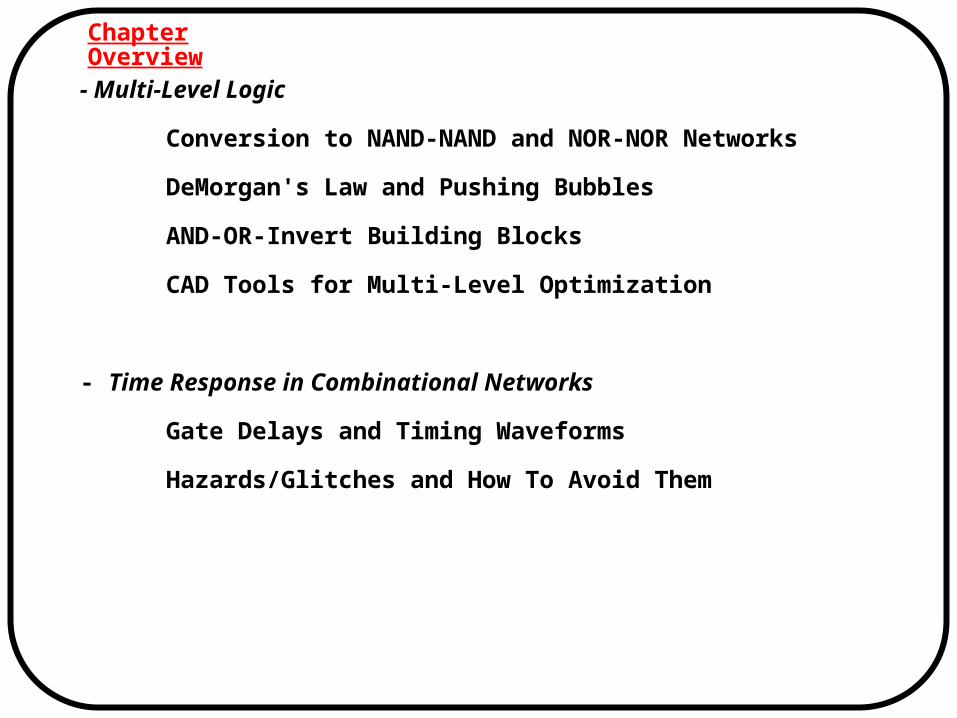
Chapter Overview
- Multi-Level Logic
Conversion to NAND-NAND and NOR-NOR Networks
DeMorgan's Law and Pushing Bubbles
AND-OR-Invert Building Blocks
CAD Tools for Multi-Level Optimization
- Time Response in Combinational Networks
Gate Delays and Timing Waveforms
Hazards/Glitches and How To Avoid Them
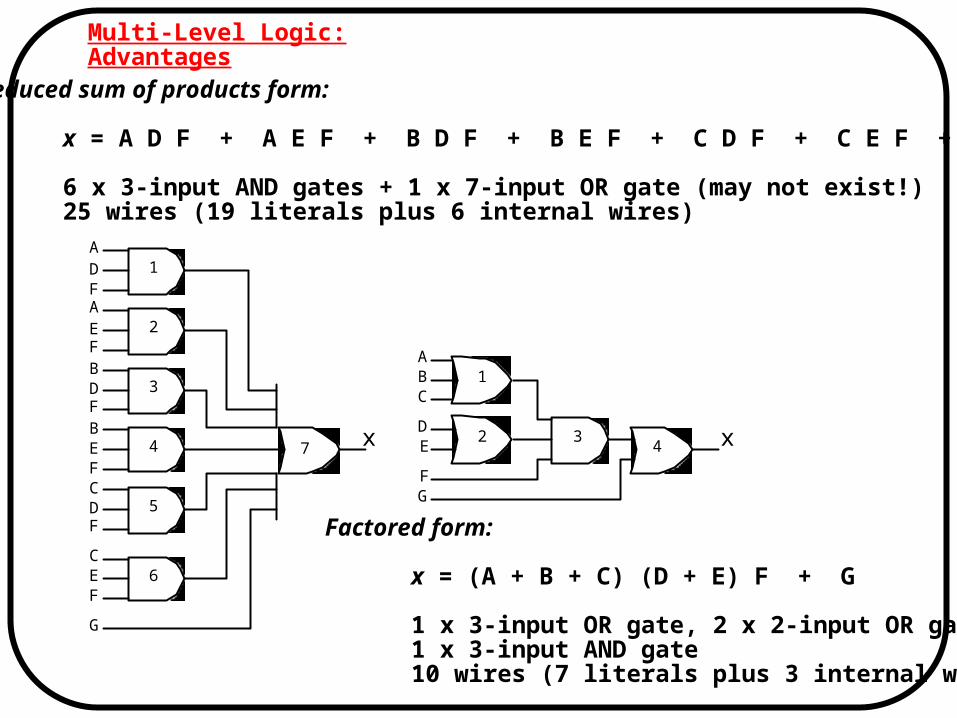
Multi-Level Logic: Advantages
Reduced sum of products form:
x = A D F + A E F + B D F + B E F + C D F + C E F + G
6 x 3-input AND gates + 1 x 7-input OR gate (may not exist!) 25 wires (19 literals plus 6 internal wires)
1
2
3
4
5
6
7
1
2 3 4
A
A
A
B
B
B
C
C
C
D
D
D
D
E
E
E
E
F
F
F
F
F
F
F
G
G
x x
Factored form:
x = (A + B + C) (D + E) F + G
1 x 3-input OR gate, 2 x 2-input OR gates, 1 x 3-input AND gate 10 wires (7 literals plus 3 internal wires)
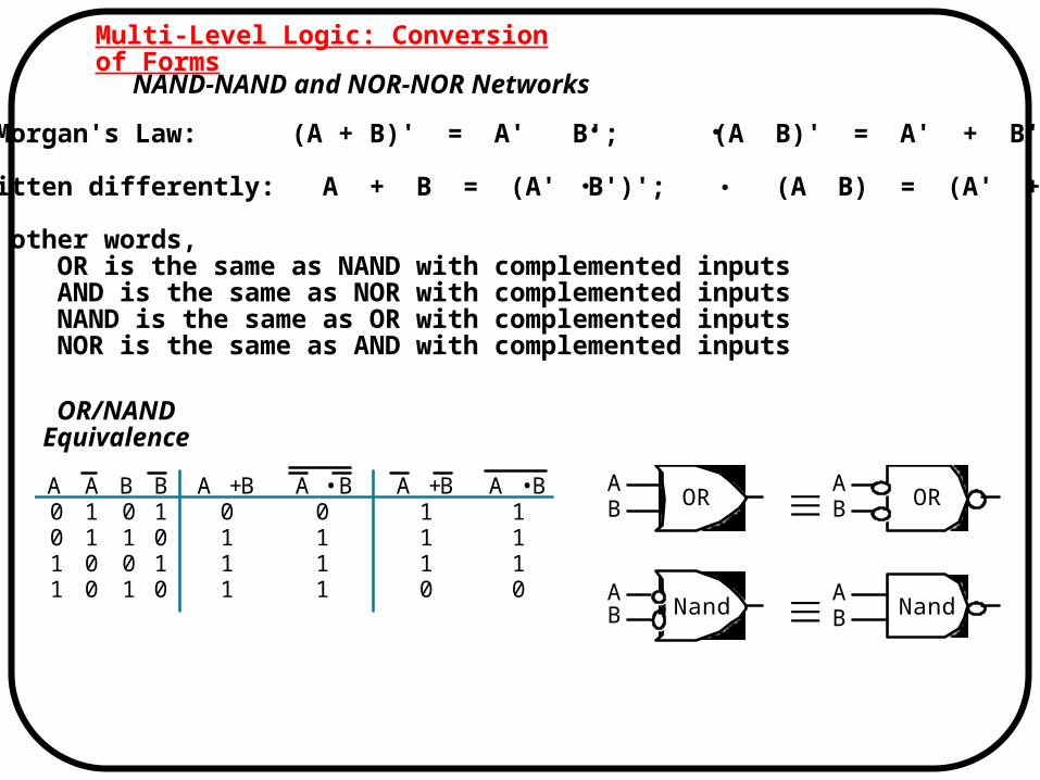
Multi-Level Logic: Conversion of Forms
NAND-NAND and NOR-NOR Networks
DeMorgan's Law: (A + B)' = A' B'; (A B)' = A' + B'
Written differently: A + B = (A' B')'; (A B) = (A' + B')'
In other words, OR is the same as NAND with complemented inputs AND is the same as NOR with complemented inputs NAND is the same as OR with complemented inputs NOR is the same as AND with complemented inputs
OR/NANDEquivalence
A A B B
A 0 0 1 1
A 1 1 0 0
B 0 1 0 1
B 1 0 1 0
A + B 0 1 1 1
A • B 0 1 1 1 A A
B B
A + B 1 1 1 0
A • B 1 1 1 0
OR OR
Nand Nand
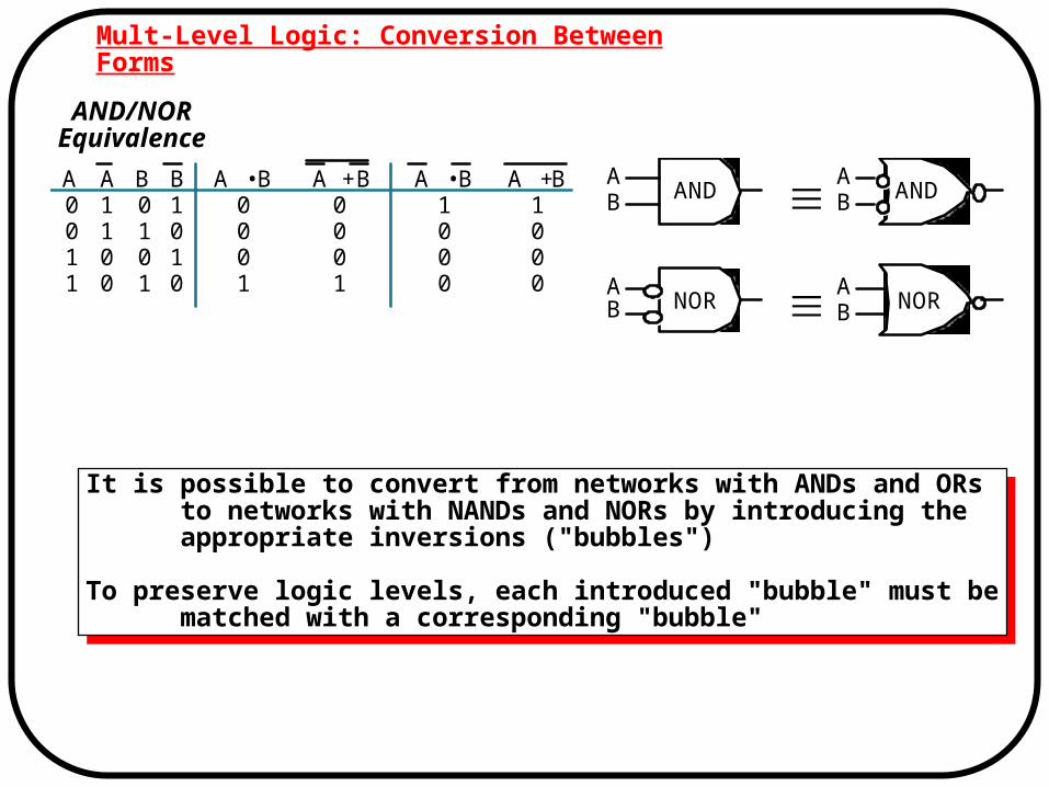
Mult-Level Logic: Conversion Between Forms
AND/NOREquivalence
It is possible to convert from networks with ANDs and ORs to networks with NANDs and NORs by introducing the appropriate inversions ("bubbles")
To preserve logic levels, each introduced "bubble" must be matched with a corresponding "bubble"
It is possible to convert from networks with ANDs and ORs to networks with NANDs and NORs by introducing the appropriate inversions ("bubbles")
To preserve logic levels, each introduced "bubble" must be matched with a corresponding "bubble"
A A B B
A 0 0 1 1
A 1 1 0 0
B 0 1 0 1
B 1 0 1 0
A • B 0 0 0 1
A + B 0 0 0 1 A A
B B
A • B 1 0 0 0
A + B 1 0 0 0
AND AND
NOR NOR
A A B B
C C D D
A B
C D
A B
C D
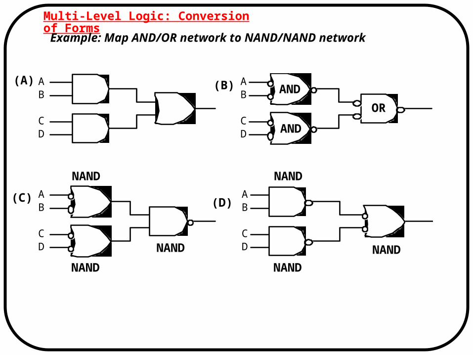
Multi-Level Logic: Conversion of Forms
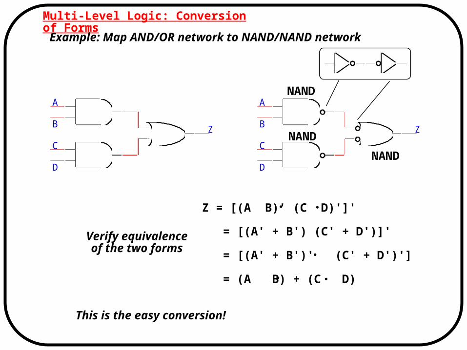
Example: Map AND/OR network to NAND/NAND network
NAND
NAND
NAND
AND
AND
OR
NAND
NAND
NAND
(A)
(C)
(B)
(D)
Multi-Level Logic: Conversion of Forms
Example: Map AND/OR network to NAND/NAND network
Z = [(A B)' (C D)']'
= [(A' + B') (C' + D')]'
= [(A' + B')' (C' + D')']
= (A B) + (C D)
Verify equivalenceof the two forms
This is the easy conversion!
NAND
NAND
NAND
AA
BB
CC
DD
ZZ
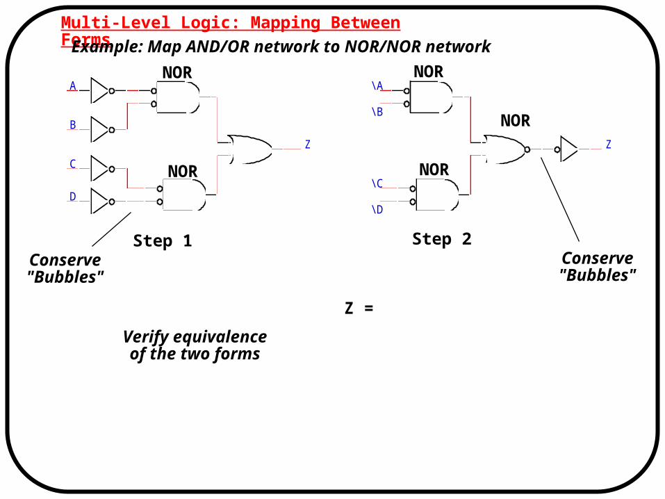
Multi-Level Logic: Mapping Between FormsExample: Map AND/OR network to NOR/NOR network
Step 1 Step 2
NOR
NOR
Conserve"Bubbles"
NOR
NOR
NOR
Conserve"Bubbles"
Verify equivalenceof the two forms
Z =
A \A
B\B
C
\CD
\D
ZZ

Multi-Level Logic: Mapping Between FormsExample: Map AND/OR network to NOR/NOR network
Step 1 Step 2Conserve"Bubbles"
Conserve"Bubbles"
Verify equivalenceof the two forms
Z = {[(A' + B')' + (C' + D')']'}'
= {(A' + B') (C' + D')}'
= (A' + B')' + (C' + D')'
= (A B) + (C D)
This is the hard conversion! AND/OR to NAND/NAND more naturalAND/OR to NAND/NAND more natural
NOR
NOR
NOR
NOR
NOR
A \A
B\B
C
\CD
\D
ZZ
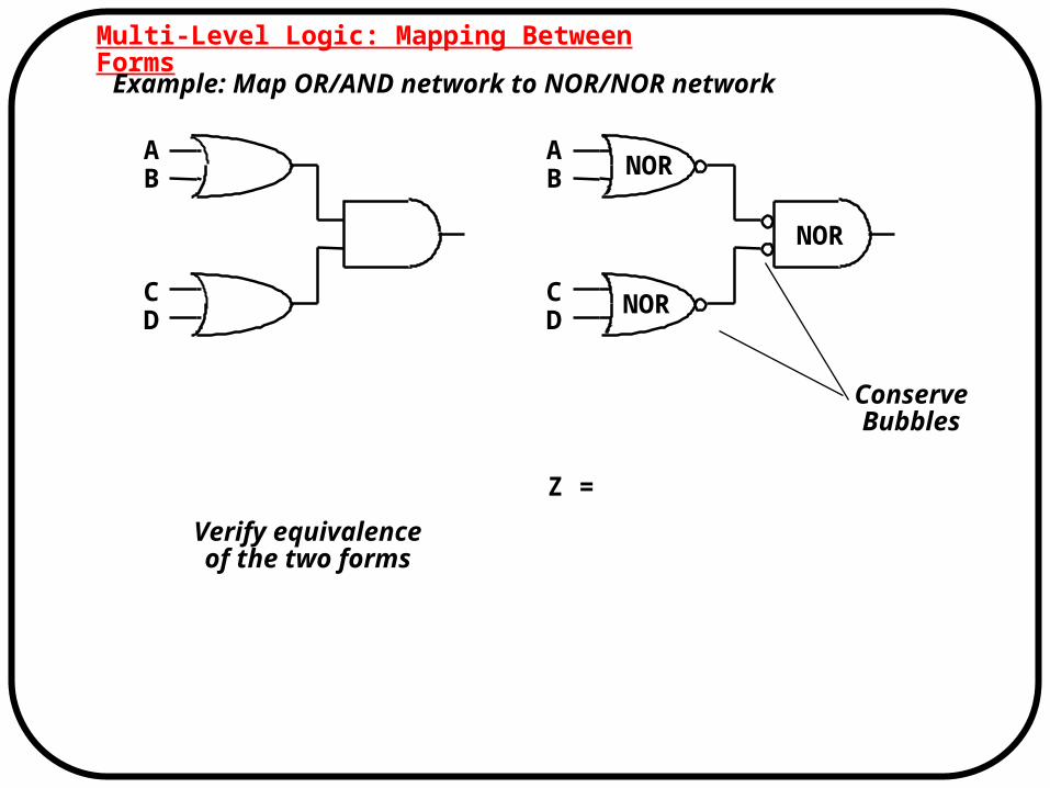
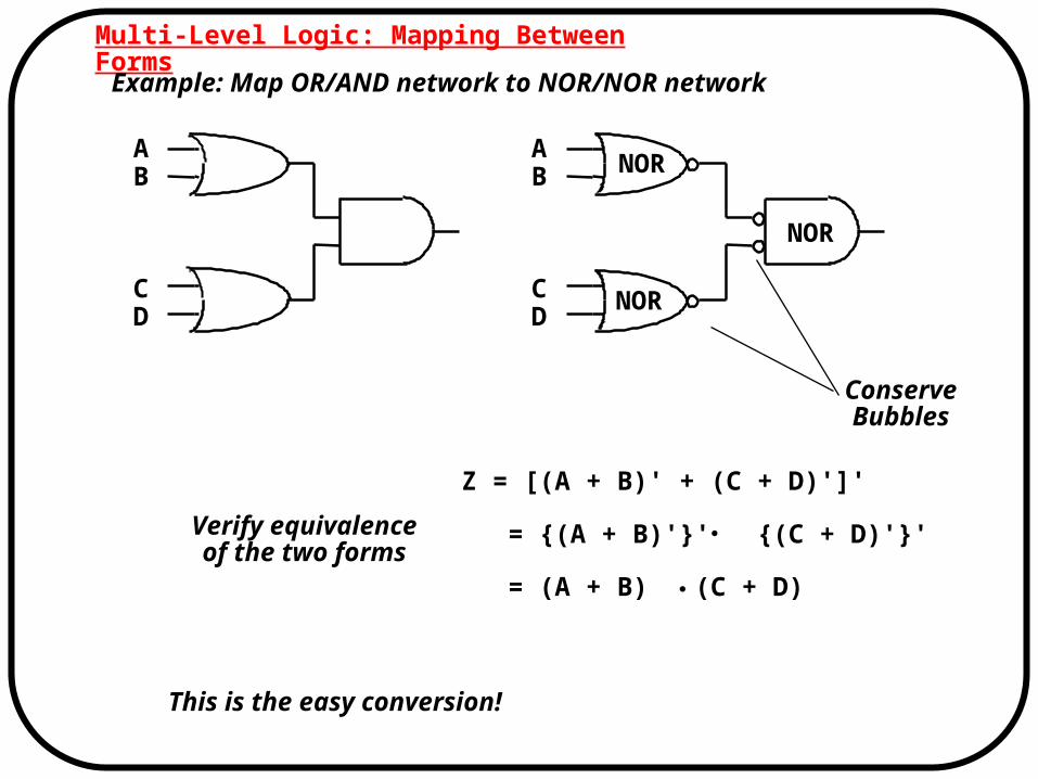
Multi-Level Logic: Mapping Between FormsExample: Map OR/AND network to NOR/NOR network
NOR
NOR
NOR
ConserveBubbles
Verify equivalenceof the two forms
Z =
AB
CD
AB
CD
Multi-Level Logic: Mapping Between FormsExample: Map OR/AND network to NOR/NOR network
NOR
NOR
NOR
ConserveBubbles
Verify equivalenceof the two forms
Z = [(A + B)' + (C + D)']'
= {(A + B)'}' {(C + D)'}'
= (A + B) (C + D)
This is the easy conversion!
AB
CD
AB
CD
Multi-Level Logic: Mapping Between Forms
Example: Map OR/AND network to NAND/NAND network
Step 1 Step 2
Nand
NandNand
Nand
Nand
ConserveBubbles!
ConserveBubbles!
Verify equivalenceof the two forms
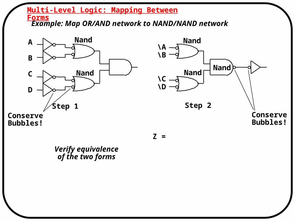
Z =
A
B
C
D
\A\B
\C\D
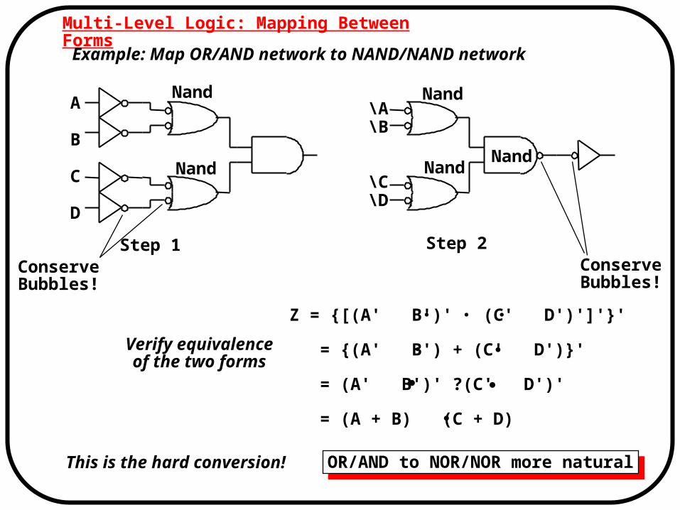
Multi-Level Logic: Mapping Between Forms
Example: Map OR/AND network to NAND/NAND network
This is the hard conversion! OR/AND to NOR/NOR more naturalOR/AND to NOR/NOR more natural
Step 1 Step 2
Nand
NandNand
Nand
Nand
ConserveBubbles!
ConserveBubbles!
Verify equivalenceof the two forms
Z = {[(A' B')' (C' D')']'}'
= {(A' B') + (C' D')}'
= (A' B')' ?(C' D')'
= (A + B) (C + D)
A
B
C
D
\A\B
\C\D
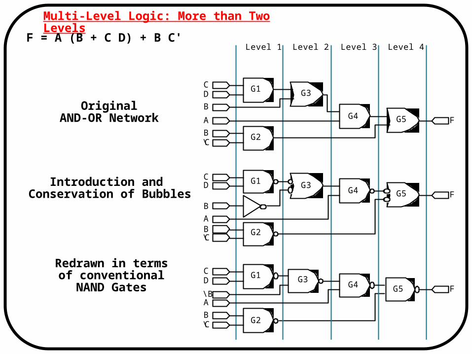
Multi-Level Logic: More than Two LevelsF = A (B + C D) + B C'
OriginalAND-OR Network
Introduction and Conservation of Bubbles
Redrawn in termsof conventional
NAND Gates
C
Level 1 Level 2 Level 3 Level 4
G1 D
B
A F G5 G4
G3
B G2 \ C
C G1 D
B
A
F G5 G4 G3
B G2 \ C
C G1 D
\B A
F G5 G4 G3
B G2 \ C
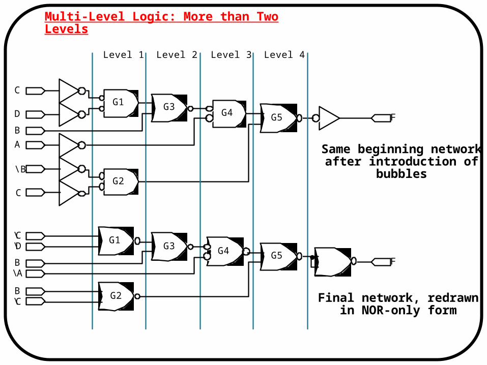
Multi-Level Logic: More than Two Levels
Same beginning networkafter introduction of
bubbles
Final network, redrawnin NOR-only form
C
Level 1 Level 2 Level 3 Level 4
G1 D
B
A
F G5 G4 G3
\B
C G2
\ C G1 \ D
B \ A
F G5 G4 G3
B \ C
G2
A
B C
D
F
A
B C
\D
F
X
\ X
(a) (b)
A
B C
D
F X
(d)
A
B C
\ D
F
(c)
\ X
X
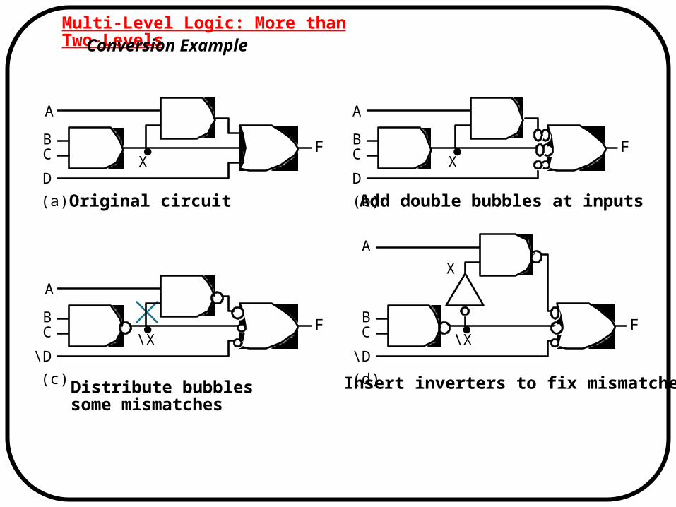
Multi-Level Logic: More than Two-LevelsConversion Example
Original circuit Add double bubbles at inputs
Distribute bubblessome mismatches
Insert inverters to fix mismatches
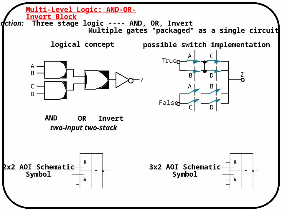
Multi-Level Logic: AND-OR-Invert Block
AOI Function: Three stage logic ---- AND, OR, Invert Multiple gates "packaged" as a single circuit block
AND OR Invert
logical concept possible switch implementation
two-input two-stack
&
&
+2x2 AOI Schematic
Symbol
&
&
+3x2 AOI Schematic
Symbol
A B
C D
Z
T rue A C
B D Z
False
A B
C D
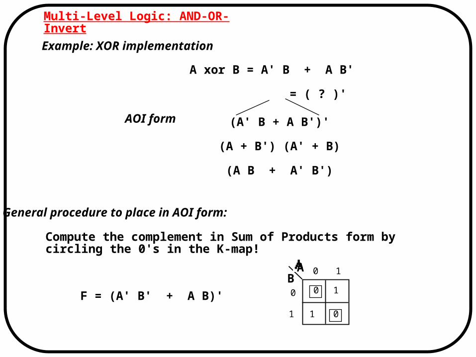
Multi-Level Logic: AND-OR-Invert
Example: XOR implementation
A xor B = A' B + A B'
= ( ? )'
(A' B + A B')'
(A + B') (A' + B)
(A B + A' B')
AOI form
General procedure to place in AOI form:
Compute the complement in Sum of Products form by circling the 0's in the K-map!
F = (A' B' + A B)'
AB
0
0
1
1
0
1
0 1
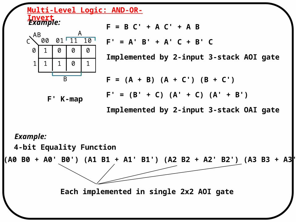
Multi-Level Logic: AND-OR-Invert
F = B C' + A C' + A B
F' = A' B' + A' C + B' C
Implemented by 2-input 3-stack AOI gate
F = (A + B) (A + C') (B + C')
F' = (B' + C) (A' + C) (A' + B')
Implemented by 2-input 3-stack OAI gate
Example:
Example:
4-bit Equality Function
Z = (A0 B0 + A0' B0') (A1 B1 + A1' B1') (A2 B2 + A2' B2') (A3 B3 + A3' B3')
Each implemented in single 2x2 AOI gate
10
1
1
0 0 0
0 1 1
B
11 01 00 AB A
C 0
1
F' K-map
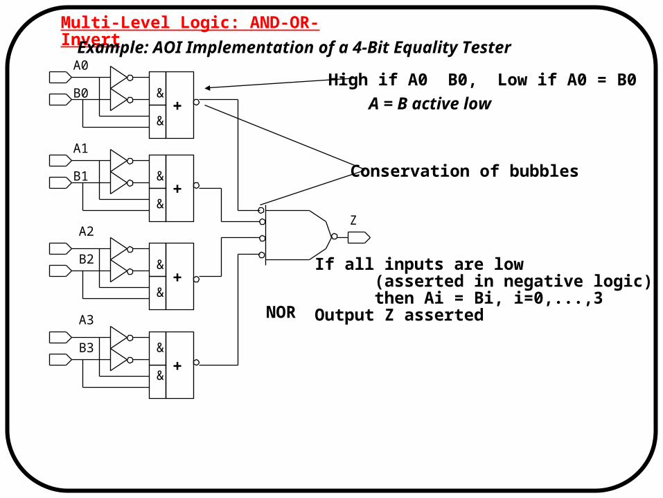
Multi-Level Logic: AND-OR-InvertExample: AOI Implementation of a 4-Bit Equality Tester
High if A0 B0, Low if A0 = B0
A = B active low
NOR
If all inputs are low (asserted in negative logic) then Ai = Bi, i=0,...,3Output Z asserted
Conservation of bubbles
&
&
&
&
&
&
&
&
+
+
+
+
A0
B0
A1
B1
A2
B2
A3
B3
Z
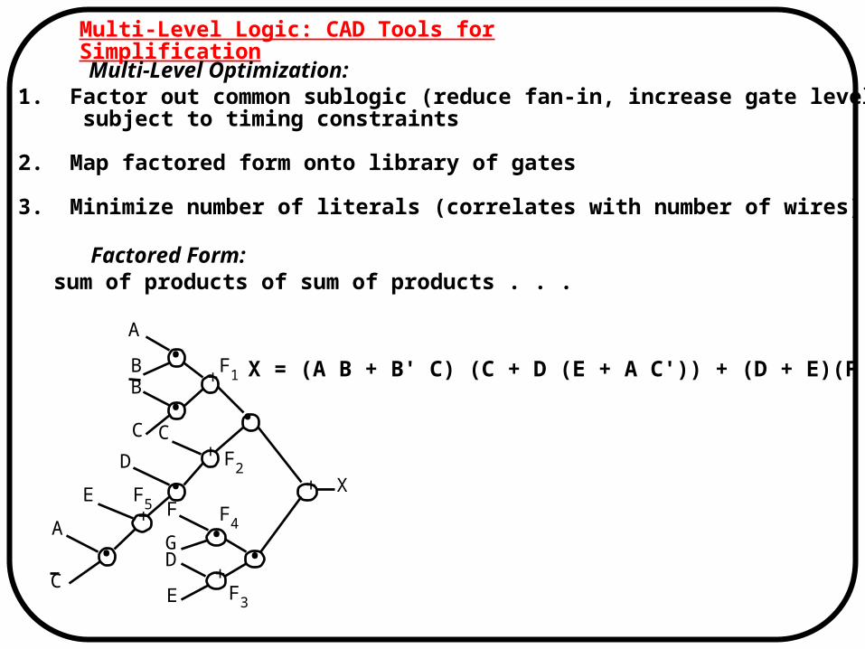
Multi-Level Logic: CAD Tools for SimplificationMulti-Level Optimization:
1. Factor out common sublogic (reduce fan-in, increase gate levels), subject to timing constraints
2. Map factored form onto library of gates
3. Minimize number of literals (correlates with number of wires)
Factored Form:sum of products of sum of products . . .
X = (A B + B' C) (C + D (E + A C')) + (D + E)(F G)
A
B B
C C
D
E
A
C
F
G D
E
F 1
F 2
F 5 F 4
F 3
X
+
+
+
+
+
•
• ••
•
••
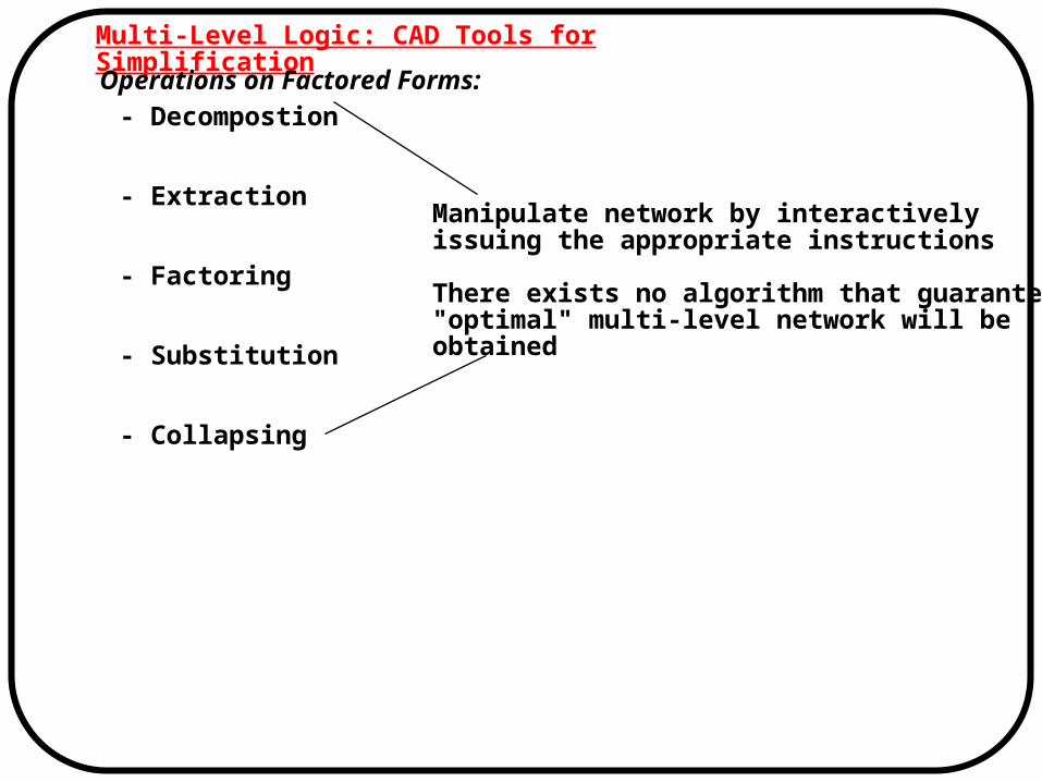
Multi-Level Logic: CAD Tools for SimplificationOperations on Factored Forms:
- Decompostion
- Extraction
- Factoring
- Substitution
- Collapsing
Manipulate network by interactivelyissuing the appropriate instructions
There exists no algorithm that guarantees"optimal" multi-level network will be obtained
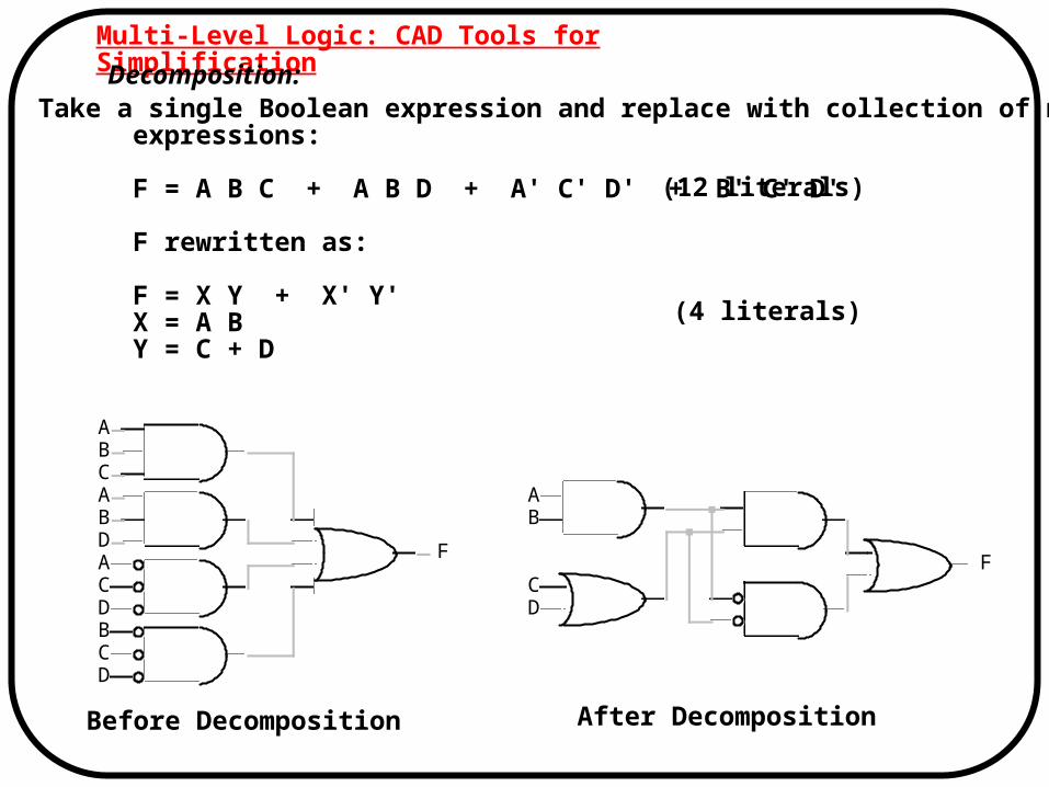
Multi-Level Logic: CAD Tools for SimplificationDecomposition:
Take a single Boolean expression and replace with collection of new expressions:
F = A B C + A B D + A' C' D' + B' C' D'
F rewritten as:
F = X Y + X' Y' X = A B Y = C + D
(12 literals)
(4 literals)
Before Decomposition After Decomposition
FF
A
A
A
A
B
B
B
B
C
C
C
C
D
D
D
D
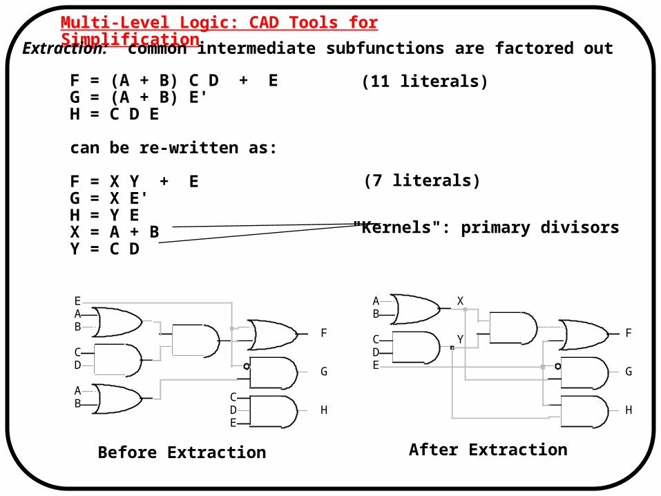
Multi-Level Logic: CAD Tools for SimplificationExtraction: common intermediate subfunctions are factored out
F = (A + B) C D + EG = (A + B) E'H = C D E
can be re-written as:
F = X Y + EG = X E'H = Y EX = A + BY = C D
(11 literals)
(7 literals)
"Kernels": primary divisors
Before Extraction After Extraction
X
E
E
E
GG
Y
HH
A
A
A B
B
BC
C
C D
D
D
FF
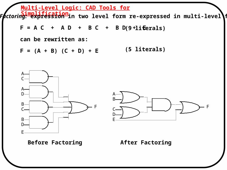
Multi-Level Logic: CAD Tools for SimplificationFactoring: expression in two level form re-expressed in multi-level form
F = A C + A D + B C + B D + E
can be rewritten as:
F = (A + B) (C + D) + E
(9 literals)
(5 literals)
Before Factoring After Factoring
AA
A
B
B
BCC
C
D
D
D
E
E
FF
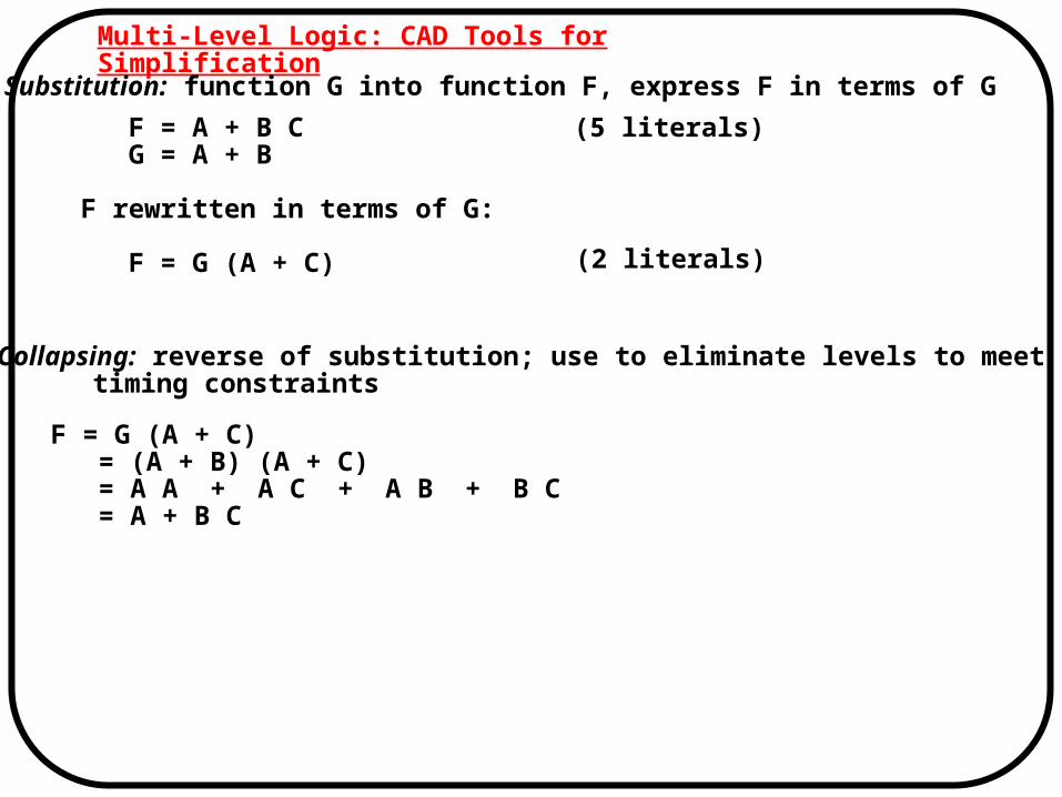
Multi-Level Logic: CAD Tools for SimplificationSubstitution: function G into function F, express F in terms of G
F = A + B C G = A + B
F rewritten in terms of G:
F = G (A + C)
Collapsing: reverse of substitution; use to eliminate levels to meet timing constraints
F = G (A + C) = (A + B) (A + C) = A A + A C + A B + B C = A + B C
(5 literals)
(2 literals)

Multi-Level Logic: CAD Tools for SimplificationKey to implementing these operations: "division" over Boolean functions
F = P Q + R
divisor quotient remainder
example:X = A C + A D + B C + B D + EY = A + B
X "divided" by Y isX = Y (C + D) + E
Complexity: finding suitable divisors
F = A D + B C D + EG = A + B
G does not divide F under algebraic division rulesG does divide F under Boolean rules (very large number of these!)
F/G = (A + C) D F = [G (A + C) D] + E = (A + B) (A + C) D + E = (A A + A C + A B + B C) D + E = (A + B C) D + E = A D + B C D + E
F written as G Q + R
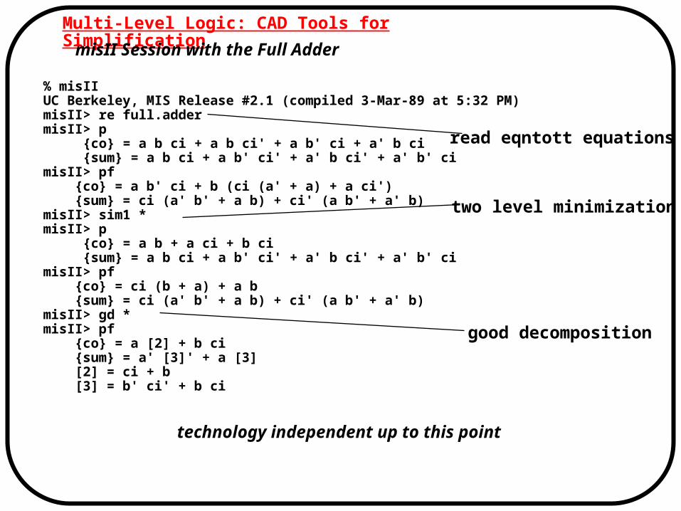
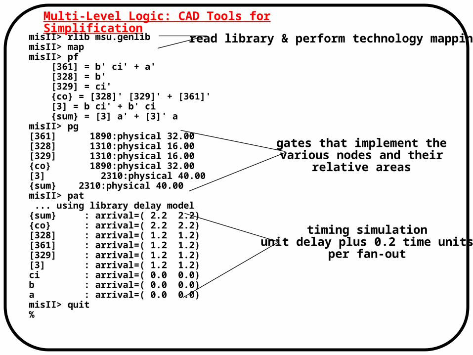
Multi-Level Logic: CAD Tools for SimplificationmisII Session with the Full Adder
% misIIUC Berkeley, MIS Release #2.1 (compiled 3-Mar-89 at 5:32 PM)misII> re full.addermisII> p {co} = a b ci + a b ci' + a b' ci + a' b ci {sum} = a b ci + a b' ci' + a' b ci' + a' b' cimisII> pf {co} = a b' ci + b (ci (a' + a) + a ci') {sum} = ci (a' b' + a b) + ci' (a b' + a' b)misII> sim1 *misII> p {co} = a b + a ci + b ci {sum} = a b ci + a b' ci' + a' b ci' + a' b' cimisII> pf {co} = ci (b + a) + a b {sum} = ci (a' b' + a b) + ci' (a b' + a' b)misII> gd *misII> pf {co} = a [2] + b ci {sum} = a' [3]' + a [3] [2] = ci + b [3] = b' ci' + b ci
read eqntott equations
two level minimization
good decomposition
technology independent up to this point
Multi-Level Logic: CAD Tools for Simplification
misII> rlib msu.genlibmisII> mapmisII> pf [361] = b' ci' + a' [328] = b' [329] = ci' {co} = [328]' [329]' + [361]' [3] = b ci' + b' ci {sum} = [3] a' + [3]' amisII> pg[361] 1890:physical 32.00[328] 1310:physical 16.00[329] 1310:physical 16.00{co} 1890:physical 32.00[3] 2310:physical 40.00{sum} 2310:physical 40.00 misII> pat ... using library delay model{sum} : arrival=( 2.2 2.2) {co} : arrival=( 2.2 2.2) [328] : arrival=( 1.2 1.2) [361] : arrival=( 1.2 1.2) [329] : arrival=( 1.2 1.2) [3] : arrival=( 1.2 1.2) ci : arrival=( 0.0 0.0) b : arrival=( 0.0 0.0) a : arrival=( 0.0 0.0) misII> quit%
read library & perform technology mapping
gates that implement thevarious nodes and their
relative areas
timing simulationunit delay plus 0.2 time units
per fan-out
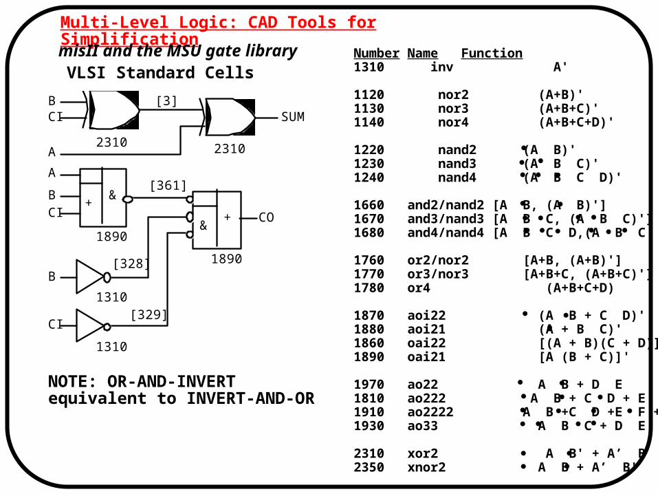
Multi-Level Logic: CAD Tools for SimplificationmisII and the MSU gate library
VLSI Standard CellsNumber Name Function1310 inv A'
1120 nor2 (A+B)'1130 nor3 (A+B+C)'1140 nor4 (A+B+C+D)'
1220 nand2 (A B)'1230 nand3 (A B C)'1240 nand4 (A B C D)'
1660 and2/nand2 [A B, (A B)']1670 and3/nand3 [A B C, (A B C)']1680 and4/nand4 [A B C D,(A B C D)']
1760 or2/nor2 [A+B, (A+B)']1770 or3/nor3 [A+B+C, (A+B+C)']1780 or4 (A+B+C+D)
1870 aoi22 (A B + C D)'1880 aoi21 (A + B C)'1860 oai22 [(A + B)(C + D)]'1890 oai21 [A (B + C)]'
1970 ao22 A B + D E1810 ao222 A B + C D + E F1910 ao2222 A B +C D +E F +G H1930 ao33 A B C + D E F
2310 xor2 A B' + A’ B2350 xnor2 A B + A’ B'
NOTE: OR-AND-INVERTequivalent to INVERT-AND-OR
B CI
[3]
2310
SUM
CO
1890
+ &
[361]
1890
& +
A
A
B CI
[328]
[329] 1310
1310
B
CI
2310
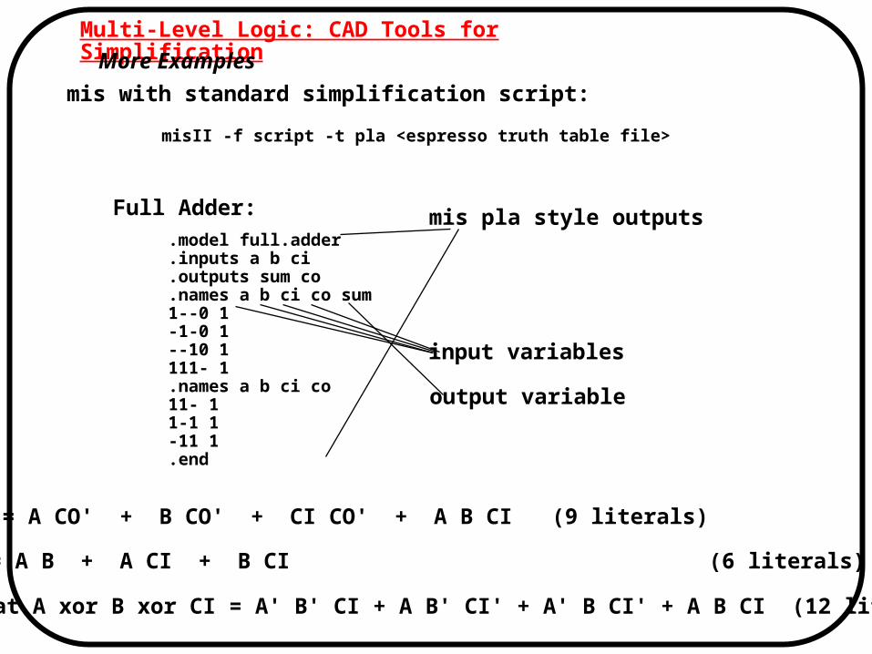
Multi-Level Logic: CAD Tools for SimplificationMore Examples
mis with standard simplification script:
misII -f script -t pla <espresso truth table file>
Full Adder:
.model full.adder
.inputs a b ci
.outputs sum co
.names a b ci co sum1--0 1-1-0 1--10 1111- 1.names a b ci co11- 11-1 1-11 1.end
mis pla style outputs
input variables
output variable
SUM = A CO' + B CO' + CI CO' + A B CI (9 literals)
CO = A B + A CI + B CI (6 literals)
Note that A xor B xor CI = A' B' CI + A B' CI' + A' B CI' + A B CI (12 literals!)
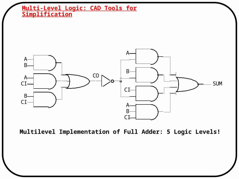
Multi-Level Logic: CAD Tools for Simplification
Multilevel Implementation of Full Adder: 5 Logic Levels!
A
A
A
A
B
B
B
B
CI
CI
CI
CI
CO
SUM

Multi-Level Logic: Tools for Simplication Two-bit Adder
.inputs a b c d
.outputs x y z
.names a c z [22] x---1 111-- 1-10- 1.names a b c d x z [22] y1---0-- 1--1---1 1-11-0-- 1--110-- 1---100- 1.names a b c d z-0-1 1-1-0 10-10 1.names a d z [22]110 1.end
Z = B' D + B D' + A' C D'
[22] = A D Z'
X = [22] + A C + C Z'
Y = A X + C [22] + B C X' + C D X' + D X' Z'
8 logic levels!
Mis Output
[22]
B
B
B
C
C
C
C
C
C
D
DD
D
D
D
Z
\X
Y
AA
A
A
X
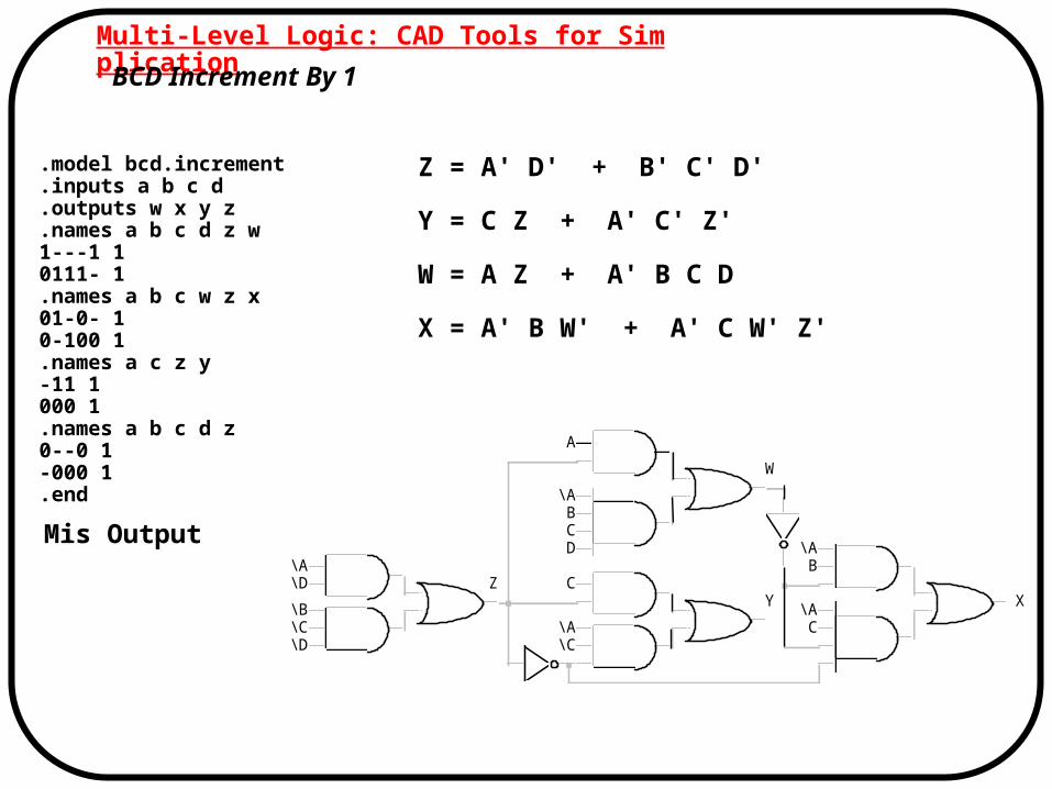
Multi-Level Logic: CAD Tools for SimplicationBCD Increment By 1
.model bcd.increment
.inputs a b c d
.outputs w x y z
.names a b c d z w1---1 10111- 1.names a b c w z x01-0- 10-100 1.names a c z y-11 1000 1.names a b c d z0--0 1-000 1.end
Mis Output
Z = A' D' + B' C' D'
Y = C Z + A' C' Z'
W = A Z + A' B C D
X = A' B W' + A' C W' Z'
Y
A
Z
DB
B
C
C
CX
W
\A\A
\A
\A
\A\B\C
\C\D
\D
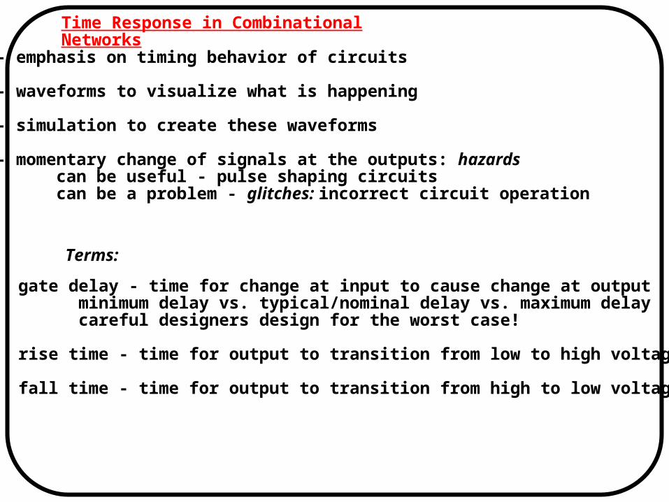
Time Response in Combinational Networks- emphasis on timing behavior of circuits
- waveforms to visualize what is happening
- simulation to create these waveforms
- momentary change of signals at the outputs: hazards can be useful - pulse shaping circuits can be a problem - glitches: incorrect circuit operation
Terms:
gate delay - time for change at input to cause change at output minimum delay vs. typical/nominal delay vs. maximum delay careful designers design for the worst case!
rise time - time for output to transition from low to high voltage
fall time - time for output to transition from high to low voltage
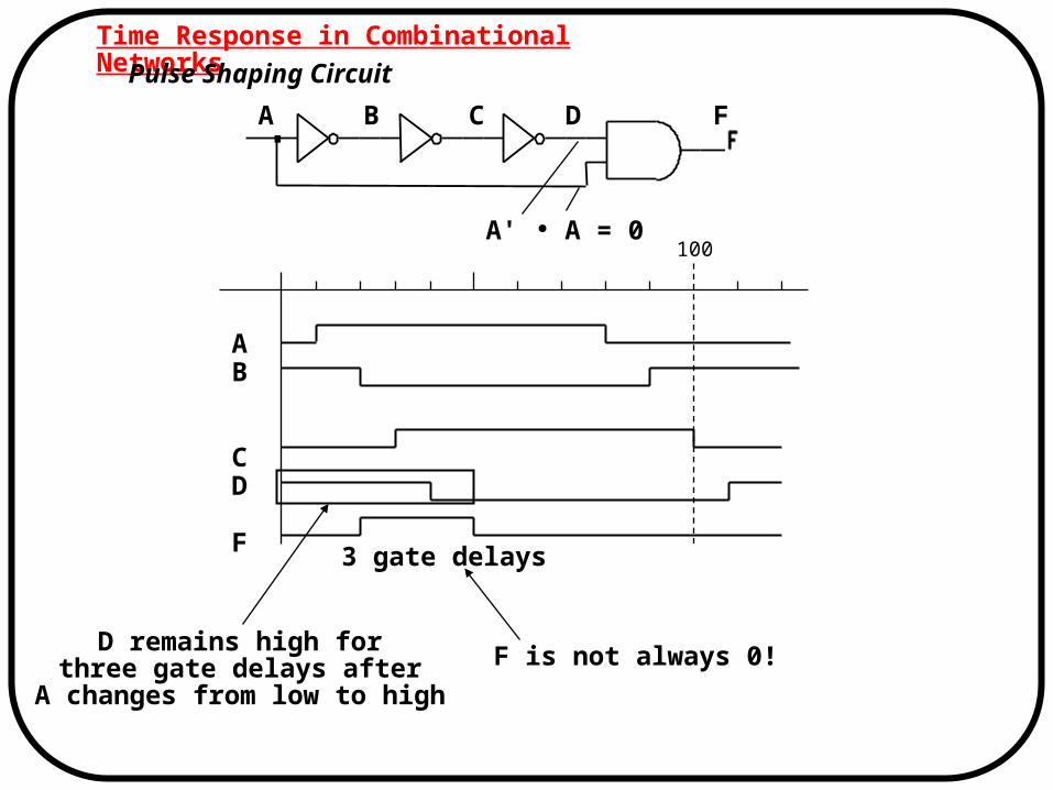
Time Response in Combinational NetworksPulse Shaping Circuit
A' A = 0
F is not always 0!
3 gate delays
D remains high forthree gate delays after
A changes from low to high
A B C D F
AB
CD
F
100
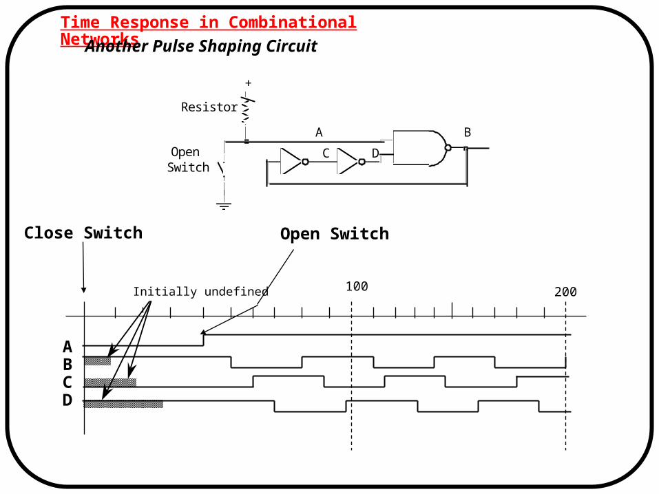
Time Response in Combinational NetworksAnother Pulse Shaping Circuit
Initially undefined
Close Switch Open Switch
+
A B
C DOpenSwitch
Resistor
ABCD
100 200
Time Response in Combinational Networks
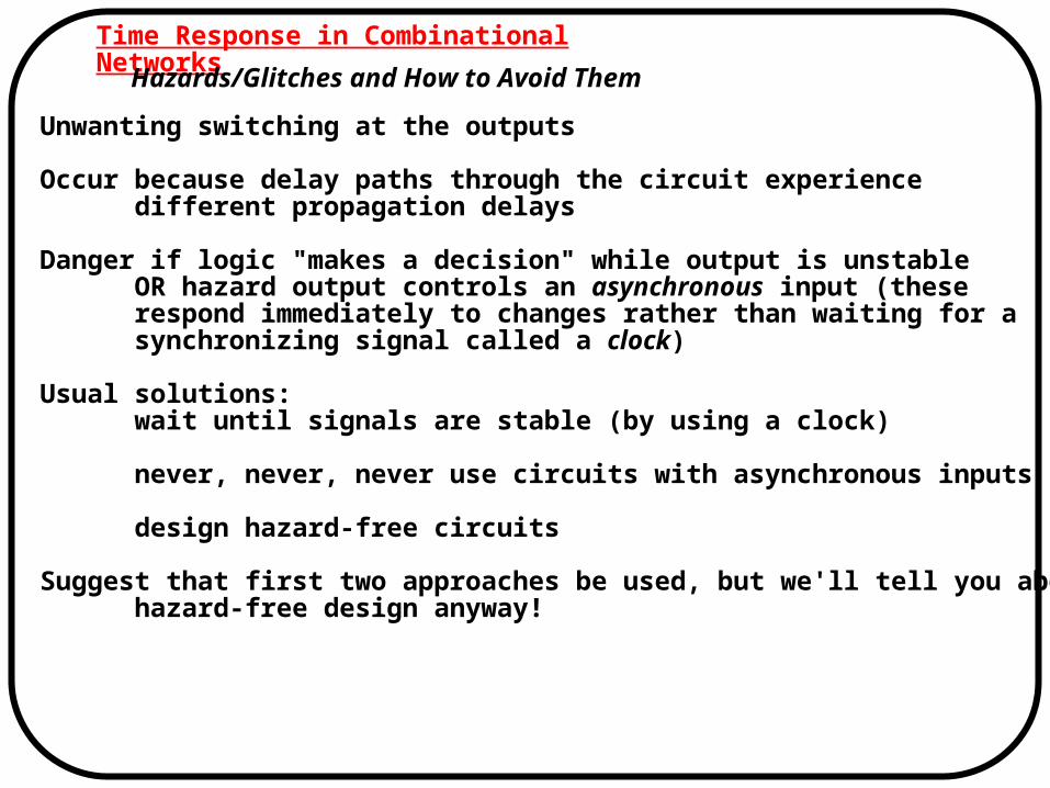
Hazards/Glitches and How to Avoid Them
Unwanting switching at the outputs
Occur because delay paths through the circuit experience different propagation delays
Danger if logic "makes a decision" while output is unstable OR hazard output controls an asynchronous input (these respond immediately to changes rather than waiting for a synchronizing signal called a clock)
Usual solutions: wait until signals are stable (by using a clock)
never, never, never use circuits with asynchronous inputs
design hazard-free circuits
Suggest that first two approaches be used, but we'll tell you about hazard-free design anyway!
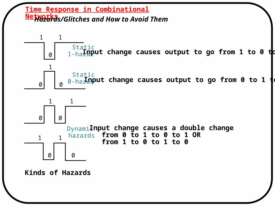
Time Response in Combinational NetworksHazards/Glitches and How to Avoid Them
Kinds of Hazards
Input change causes output to go from 1 to 0 to 1
Input change causes output to go from 0 to 1 to 0
Input change causes a double change from 0 to 1 to 0 to 1 OR from 1 to 0 to 1 to 0
Static 0-hazard
Dynamic hazards
Static 1-hazard
1 1
0
1
0 0
1
0 0
1
1 1
0 0
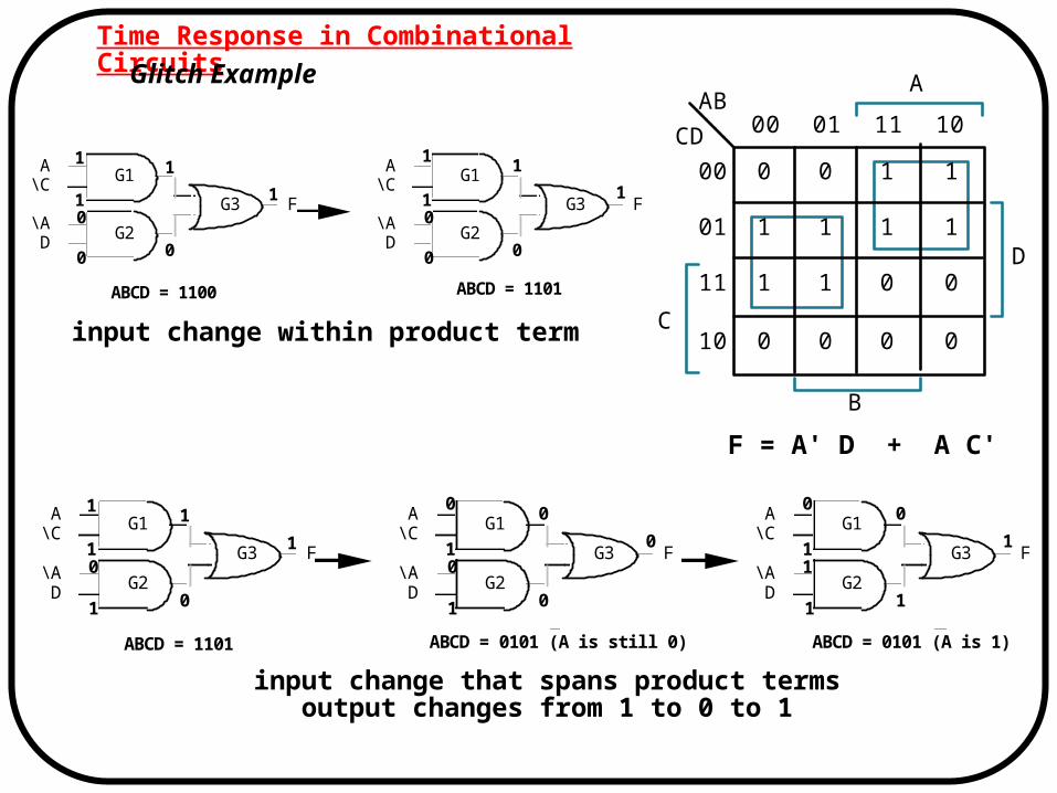
Time Response in Combinational CircuitsGlitch Example
F = A' D + A C'
input change within product term
input change that spans product termsoutput changes from 1 to 0 to 1
G1
G2
G3
A\C
\AD
F
G1
G2
G3
A\C
\AD
F
1
1
1
1
0
0
0
1
1
1
1
0
0
0
ABCD = 1100 ABCD = 1101
G1
G2
G3
A\C
\AD
F
G1
G2
G3
A\C
\AD
F
0
1
0
0
1
0
0
1
1
1
1
1
0
0
ABCD = 1101 ABCD = 0101 (A is still 0)
G1
G2
G3
A\C
\AD
F
0
1
0
1
1
1
1
ABCD = 0101 (A is 1)
A AB
00 01 11 10
0 0 1 1
1 1 1 1
1 1 0 0
0 0 0 0
00
01
11
10 C
CD
D
B
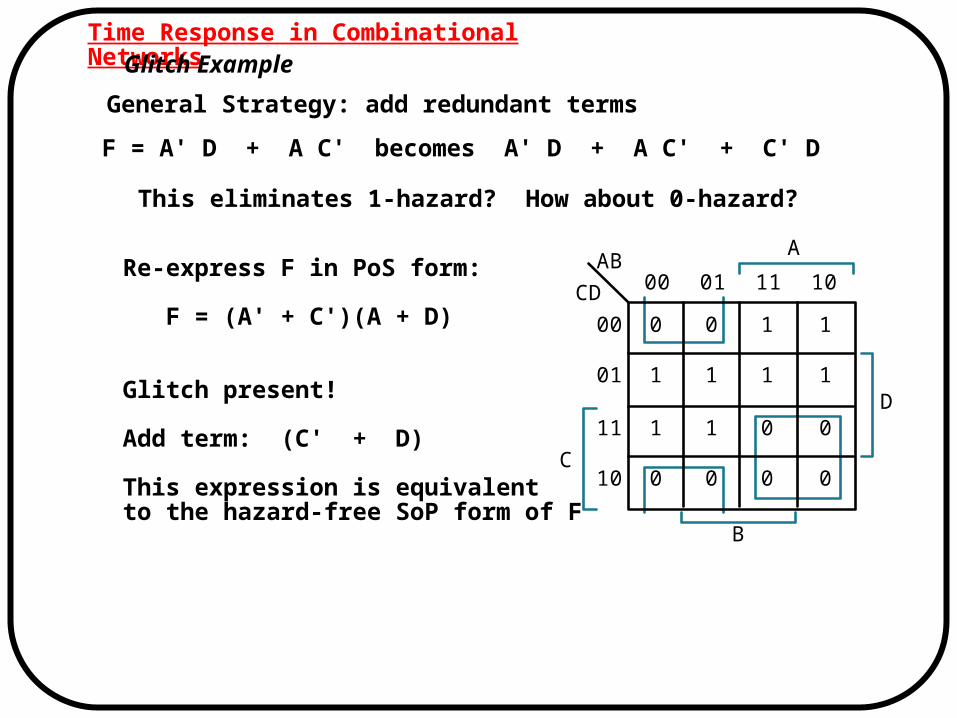
Time Response in Combinational NetworksGlitch Example
General Strategy: add redundant terms
F = A' D + A C' becomes A' D + A C' + C' D
This eliminates 1-hazard? How about 0-hazard?
Re-express F in PoS form:
F = (A' + C')(A + D)
Glitch present!
Add term: (C' + D)
This expression is equivalentto the hazard-free SoP form of F
A AB
00 01 11 10
0 0 1 1
1 1 1 1
1 1 0 0
0 0 0 0
00
01
11
10 C
CD
D
B
Time Response in Combinational NetworksGlitch Example
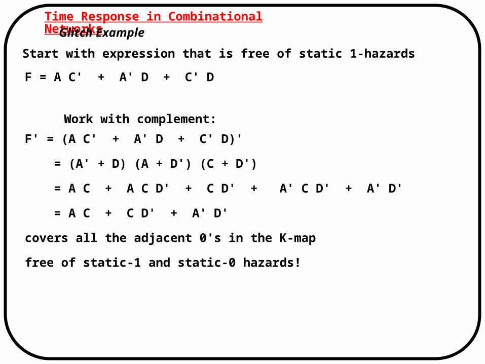
Start with expression that is free of static 1-hazards
F = A C' + A' D + C' D
F' = (A C' + A' D + C' D)'
= (A' + D) (A + D') (C + D')
= A C + A C D' + C D' + A' C D' + A' D'
= A C + C D' + A' D'
covers all the adjacent 0's in the K-map
free of static-1 and static-0 hazards!
Work with complement:
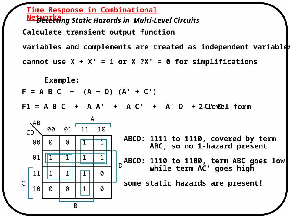
Time Response in Combinational NetworksDetecting Static Hazards in Multi-Level Circuits
Calculate transient output function
variables and complements are treated as independent variables
cannot use X + X' = 1 or X ?X' = 0 for simplifications
F = A B C + (A + D) (A' + C')
F1 = A B C + A A' + A C' + A' D + C' D
Example:
2-level form
ABCD: 1111 to 1110, covered by term ABC, so no 1-hazard present
ABCD: 1110 to 1100, term ABC goes low while term AC' goes high
some static hazards are present!
A AB
00 01 11 10
0 0 1 1
1 1 1 1
1 1 1 0
0 0 1 0
00
01
11
10 C
CD
D
B
100
A B C D F F 2
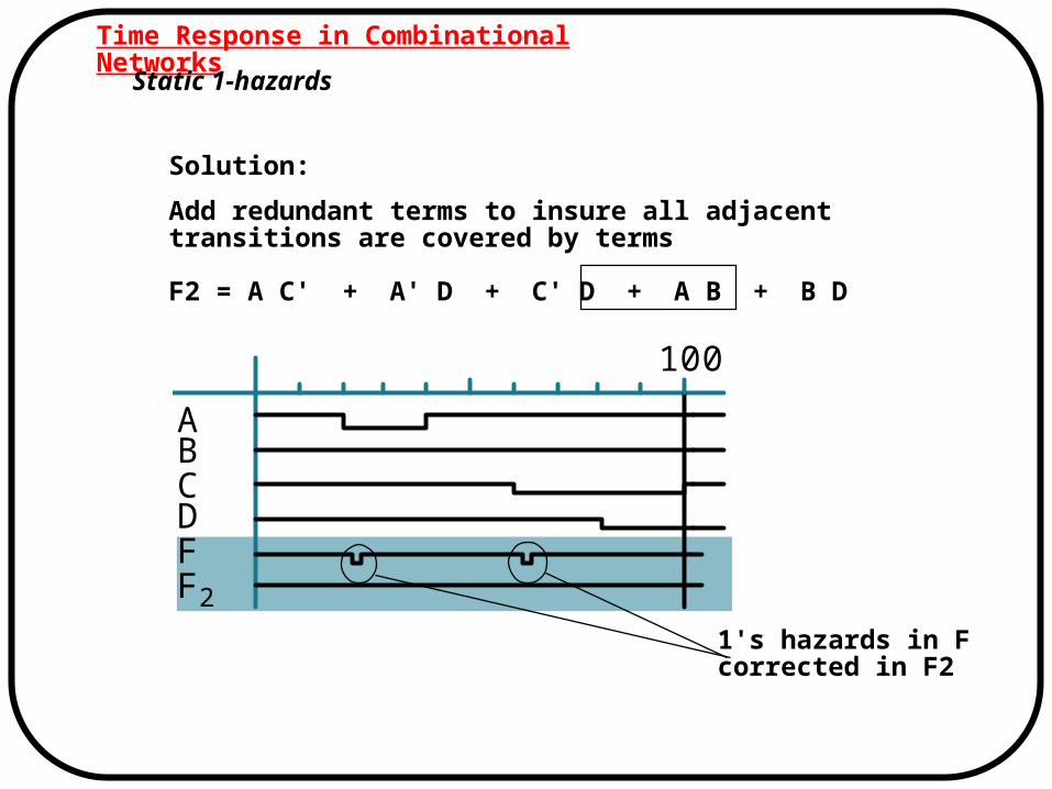
Time Response in Combinational Networks
Static 1-hazards
Solution:
Add redundant terms to insure all adjacent transitions are covered by terms
F2 = A C' + A' D + C' D + A B + B D
1's hazards in Fcorrected in F2
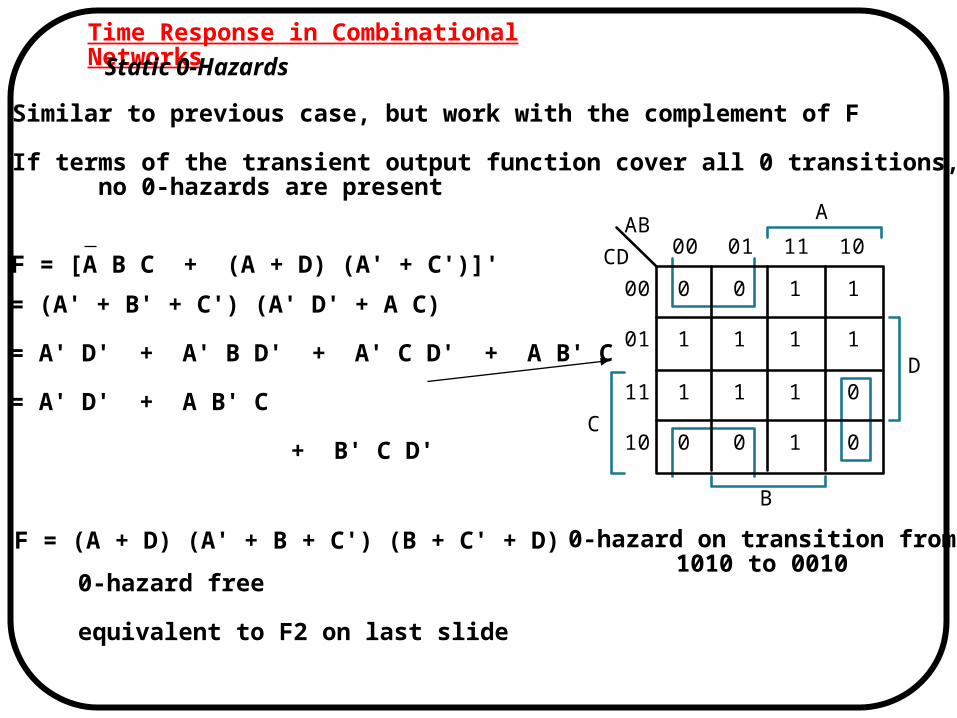
Time Response in Combinational NetworksStatic 0-Hazards
Similar to previous case, but work with the complement of F
If terms of the transient output function cover all 0 transitions, then no 0-hazards are present
F = [A B C + (A + D) (A' + C')]'
= (A' + B' + C') (A' D' + A C)
= A' D' + A' B D' + A' C D' + A B' C
= A' D' + A B' C
0-hazard on transition from1010 to 0010
+ B' C D'
F = (A + D) (A' + B + C') (B + C' + D)
0-hazard free
equivalent to F2 on last slide
A AB
00 01 11 10
0 0 1 1
1 1 1 1
1 1 1 0
0 0 1 0
00
01
11
10 C
CD
D
B

100
A B C D F F 3
Time Response in Combinational NetworksStatic 0-Hazards
0-HazardCorrected in F3
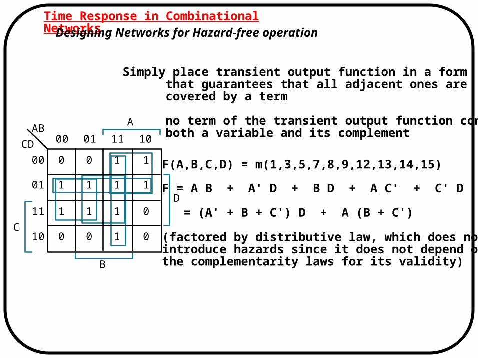
Time Response in Combinational NetworksDesigning Networks for Hazard-free operation
Simply place transient output function in a form that guarantees that all adjacent ones are covered by a term
no term of the transient output function contains both a variable and its complement
F(A,B,C,D) = m(1,3,5,7,8,9,12,13,14,15)
F = A B + A' D + B D + A C' + C' D
= (A' + B + C') D + A (B + C')
(factored by distributive law, which does notintroduce hazards since it does not depend onthe complementarity laws for its validity)
A AB
00 01 11 10
0 0 1 1
1 1 1 1
1 1 1 0
0 0 1 0
00
01
11
10 C
CD
D
B
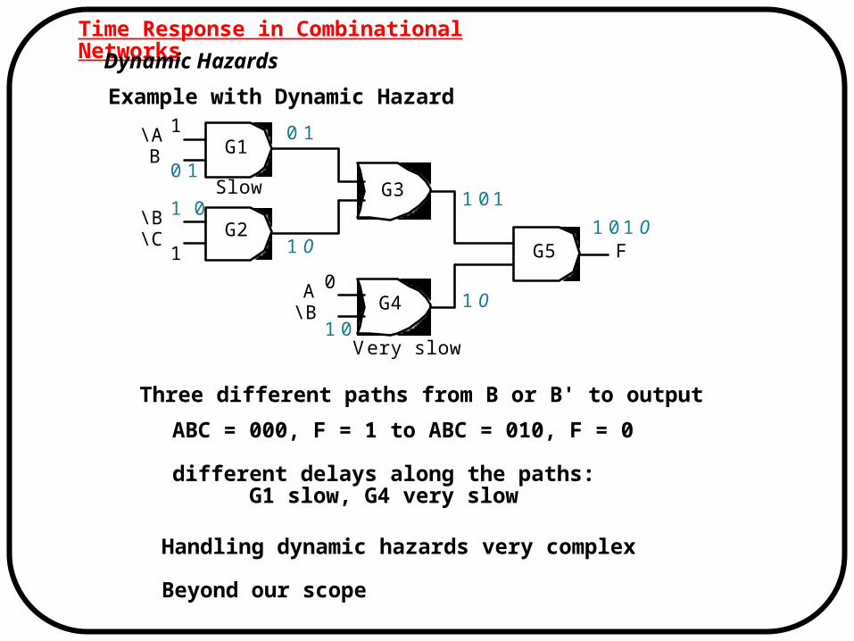
Time Response in Combinational NetworksDynamic Hazards
Example with Dynamic Hazard
Three different paths from B or B' to output
ABC = 000, F = 1 to ABC = 010, F = 0
different delays along the paths: G1 slow, G4 very slow
Handling dynamic hazards very complex
Beyond our scope
G1
G2
G3
G5
G4
\A B
\B
\B \C
F
A
0 1
1
1 0
1
0 1
1 0
1 0 1
1 0 0
1 0
1 0 1 0
Slow
V ery slow
Chapter Review
- Transition from Simple Gates to more complex gate building blocks
- Conversion from AND/OR, OR/AND to NAND/NAND, NOR/NOR
- Multi-Level Logic: Reduced gate count, fan-ins, but increased delay
- Use of misII to optimize multi-level logic and to perform mappings
- Time Response in Combinational Logic:
Gate Delay, Rise Time, Fall TimeHazards and Hazard-free Design
Recommended