CIS 371: Comp. Org. | Prof. Milo Martin | Lab Hints 1
CIS 371 Computer Organization and Design
Lab Hints
Based on slides by Prof. Amir Roth & Prof. Milo Martin
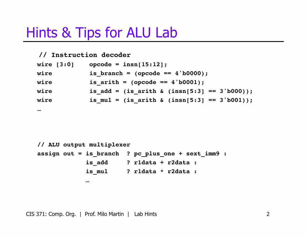
Hints & Tips for ALU Lab // Instruction decoder! wire [3:0] opcode = insn[15:12];! wire is_branch = (opcode == 4'b0000); ! wire is_arith = (opcode == 4'b0001);! wire is_add = (is_arith & (insn[5:3] == 3'b000));! wire is_mul = (is_arith & (insn[5:3] == 3'b001));! …!
// ALU output multiplexer ! assign out = is_branch ? pc_plus_one + sext_imm9 :! is_add ? r1data + r2data :! is_mul ? r1data * r2data :! …!
CIS 371: Comp. Org. | Prof. Milo Martin | Lab Hints 2
PC
Memory 216 by 16 bit
16 16
16
3’b111
insn[11:9] 3
Branch Logic
16
16
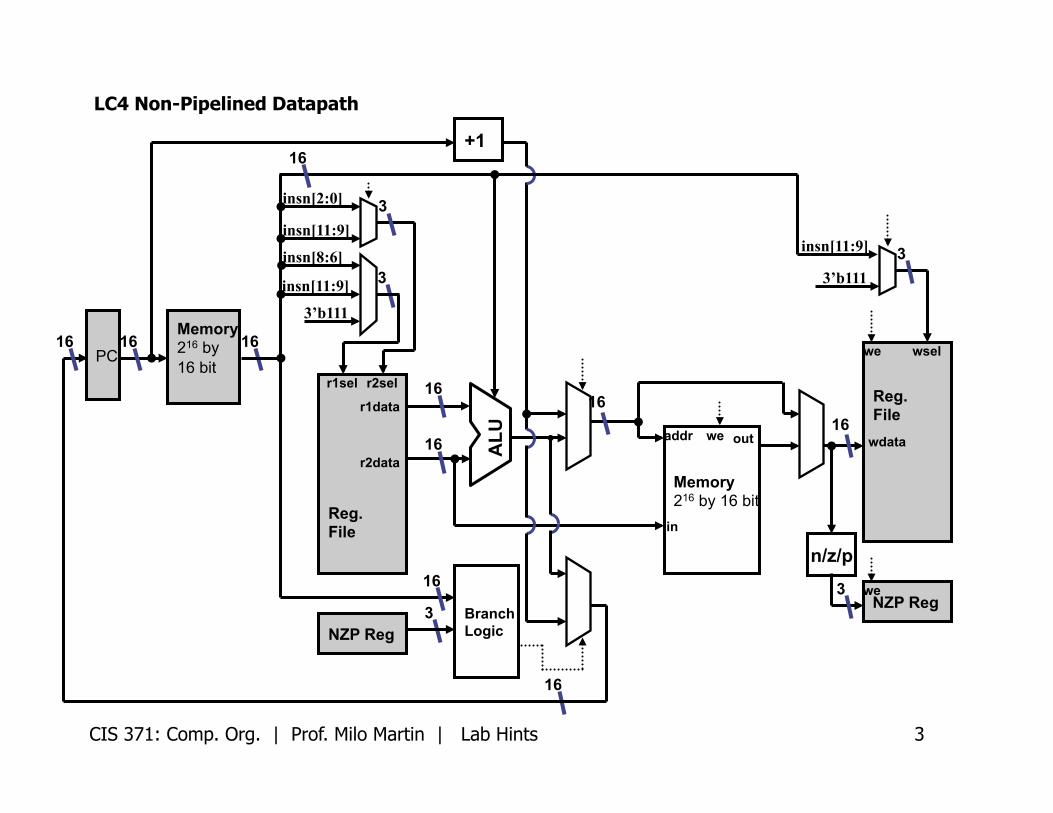
LC4 Non-Pipelined Datapath
Reg. File
wdata
3’b111
insn[11:9] 3
insn[11:9]
insn[2:0] 3
Reg. File
r1sel r2sel
r1data
r2data
wsel we
NZP Reg we
NZP Reg 3
16
16
16
Memory 216 by 16 bit
in
outaddr we
16
n/z/p
3
insn[8:6]
16
ALU
+1
3 CIS 371: Comp. Org. | Prof. Milo Martin | Lab Hints
CIS 371: Comp. Org. | Prof. Milo Martin | Lab Hints 4
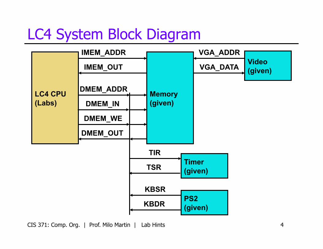
LC4 System Block Diagram
LC4 CPU (Labs)
Memory (given)
IMEM_ADDR
IMEM_OUT
DMEM_ADDR
DMEM_IN
DMEM_WE
DMEM_OUT
VGA_ADDR
VGA_DATA Video (given)
TIR
TSR
KBSR
KBDR
Timer (given)
PS2 (given)
CIS 371: Comp. Org. | Prof. Milo Martin | Lab Hints 5
Memory Module
• Processor storage • 216 location, each 16-bits • Used “Block RAM” on the FPGAs
• Memory mapped I/O • Memory mapped display (much like LC-3)
• Only difference: 128x120 (rather than 128x124) • Timer registers • Keyboard registers • Read switches • Set LEDs • Set 7-segment display
• Like “register”, memory specified using behavioral Verilog
CIS 371: Comp. Org. | Prof. Milo Martin | Lab Hints 6
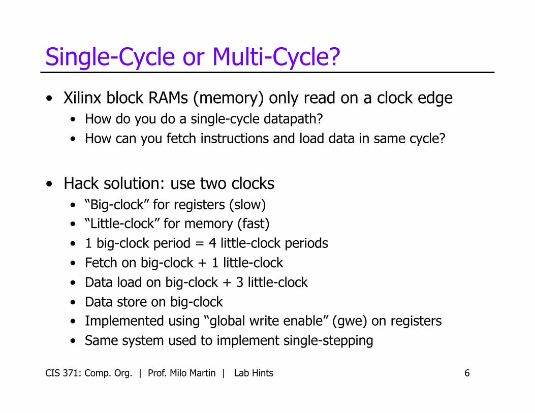
Single-Cycle or Multi-Cycle?
• Xilinx block RAMs (memory) only read on a clock edge • How do you do a single-cycle datapath? • How can you fetch instructions and load data in same cycle?
• Hack solution: use two clocks • “Big-clock” for registers (slow) • “Little-clock” for memory (fast) • 1 big-clock period = 4 little-clock periods • Fetch on big-clock + 1 little-clock • Data load on big-clock + 3 little-clock • Data store on big-clock • Implemented using “global write enable” (gwe) on registers • Same system used to implement single-stepping
CIS 371: Comp. Org. | Prof. Milo Martin | Lab Hints 7
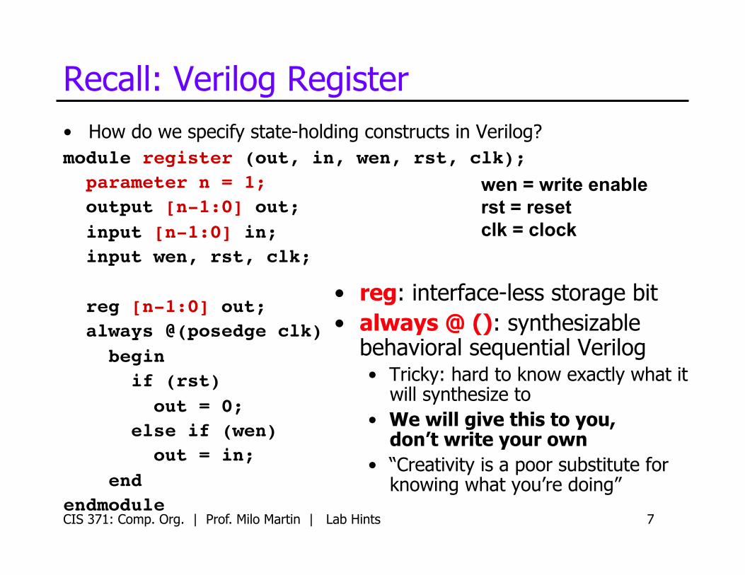
Recall: Verilog Register • How do we specify state-holding constructs in Verilog? module register (out, in, wen, rst, clk); ! parameter n = 1; ! output [n-1:0] out; ! input [n-1:0] in; ! input wen, rst, clk; !
reg [n-1:0] out; ! always @(posedge clk)! begin! if (rst)! out = 0;! else if (wen)! out = in;! end !endmodule !
wen = write enable rst = reset clk = clock
• reg: interface-less storage bit • always @ (): synthesizable
behavioral sequential Verilog • Tricky: hard to know exactly what it
will synthesize to • We will give this to you,
don’t write your own • “Creativity is a poor substitute for
knowing what you’re doing”!
CIS 371: Comp. Org. | Prof. Milo Martin | Lab Hints 8
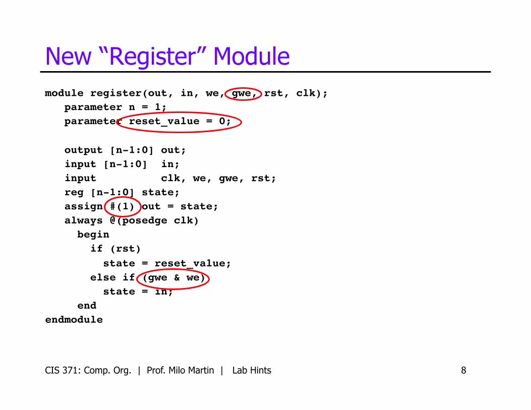
New “Register” Module module register(out, in, we, gwe, rst, clk);! parameter n = 1;! parameter reset_value = 0;!
output [n-1:0] out;! input [n-1:0] in; ! input clk, we, gwe, rst;! reg [n-1:0] state;! assign #(1) out = state;! always @(posedge clk) ! begin ! if (rst) ! state = reset_value;! else if (gwe & we) ! state = in; ! end!endmodule!
CIS 371: Comp. Org. | Prof. Milo Martin | Lab Hints 9
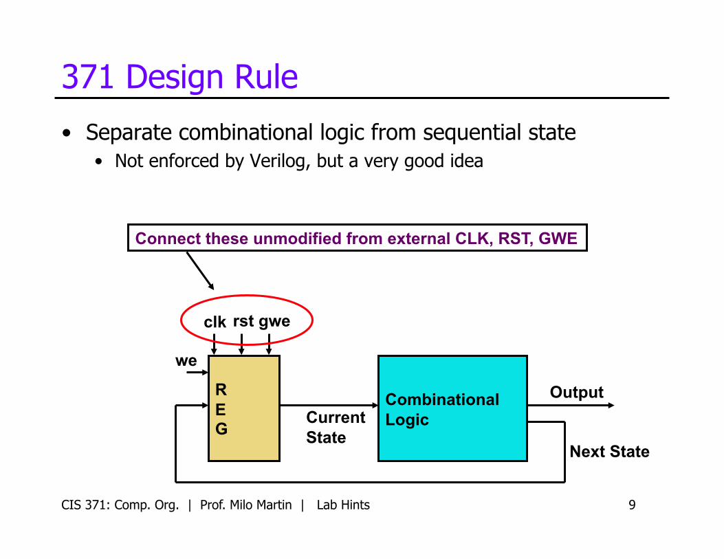
371 Design Rule
• Separate combinational logic from sequential state • Not enforced by Verilog, but a very good idea
Combinational Logic
R E G
Output
Next State
Current State
clk rst gwe
Connect these unmodified from external CLK, RST, GWE
we
CIS 371: Comp. Org. | Prof. Milo Martin | Lab Hints 10
Clock • The clock signals are not normal signals
• Travel on dedicated “clock” wires • Reach all parts of the FPGA • Special “low-skew” routing
• Messing with the clock can cause a errors • Often can only be found using timing simulation
• Never do logic operations on the clocks • Always pass them unmodified
LC4 DATAPATH SKELETON (LC4_SINGLE.V)
CIS 371: Comp. Org. | Prof. Milo Martin | Lab Hints 11
LC4 Datapath Skeleton (lc4_single.v) module lc4_processor(…); !
input clk; // main clock! input rst; // global reset! input gwe; // global we for single-step clock!
output [15:0] imem_addr; // Address to read from instruction memory! input [15:0] imem_out; // Output of instruction memory! output [15:0] dmem_addr; // Address to read/write from/to data memory! input [15:0] dmem_out; // Output of data memory! output dmem_we; // Data memory write enable! output [15:0] dmem_in; // Value to write to data memory!
CIS 371: Comp. Org. | Prof. Milo Martin | Lab Hints 12
• Clock/Reset/Gwe • Signals to talk to/from memory
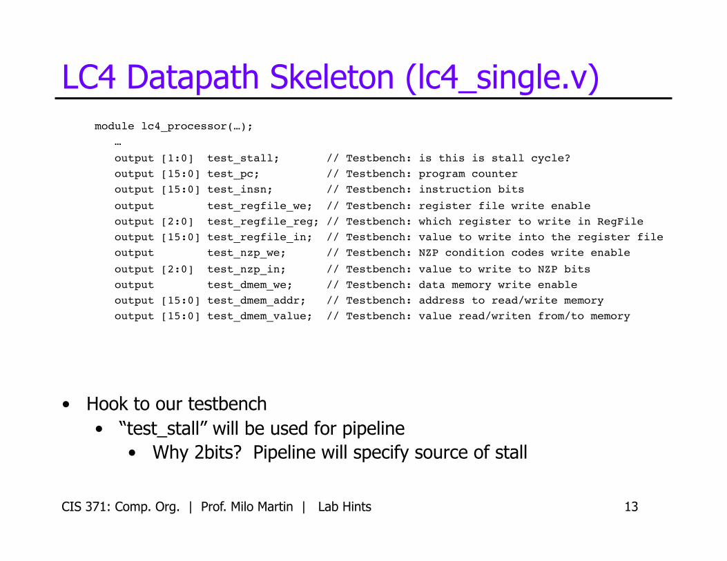
LC4 Datapath Skeleton (lc4_single.v) module lc4_processor(…); ! … !
output [1:0] test_stall; // Testbench: is this is stall cycle? ! output [15:0] test_pc; // Testbench: program counter! output [15:0] test_insn; // Testbench: instruction bits!
output test_regfile_we; // Testbench: register file write enable! output [2:0] test_regfile_reg; // Testbench: which register to write in RegFile! output [15:0] test_regfile_in; // Testbench: value to write into the register file! output test_nzp_we; // Testbench: NZP condition codes write enable!
output [2:0] test_nzp_in; // Testbench: value to write to NZP bits! output test_dmem_we; // Testbench: data memory write enable! output [15:0] test_dmem_addr; // Testbench: address to read/write memory! output [15:0] test_dmem_value; // Testbench: value read/writen from/to memory!
CIS 371: Comp. Org. | Prof. Milo Martin | Lab Hints 13
• Hook to our testbench • “test_stall” will be used for pipeline
• Why 2bits? Pipeline will specify source of stall
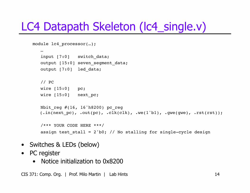
LC4 Datapath Skeleton (lc4_single.v) module lc4_processor(…); ! … ! input [7:0] switch_data;! output [15:0] seven_segment_data;! output [7:0] led_data;!
// PC! wire [15:0] pc;! wire [15:0] next_pc;!
Nbit_reg #(16, 16'h8200) pc_reg (.in(next_pc), .out(pc), .clk(clk), .we(1'b1), .gwe(gwe), .rst(rst));!
/*** YOUR CODE HERE ***/!
assign test_stall = 2'b0; // No stalling for single-cycle design!
CIS 371: Comp. Org. | Prof. Milo Martin | Lab Hints 14
• Switches & LEDs (below) • PC register
• Notice initialization to 0x8200
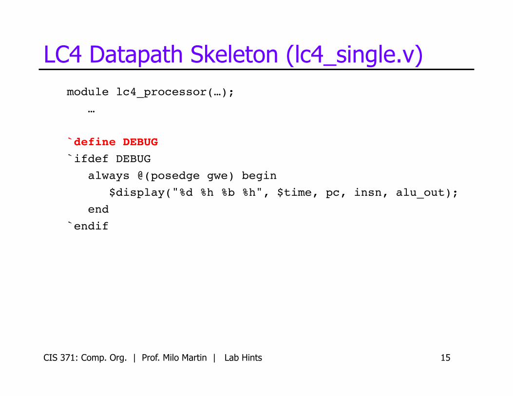
LC4 Datapath Skeleton (lc4_single.v) module lc4_processor(…); ! … !
`define DEBUG !`ifdef DEBUG! always @(posedge gwe) begin! $display("%d %h %b %h", $time, pc, insn, alu_out);! end!`endif!
CIS 371: Comp. Org. | Prof. Milo Martin | Lab Hints 15
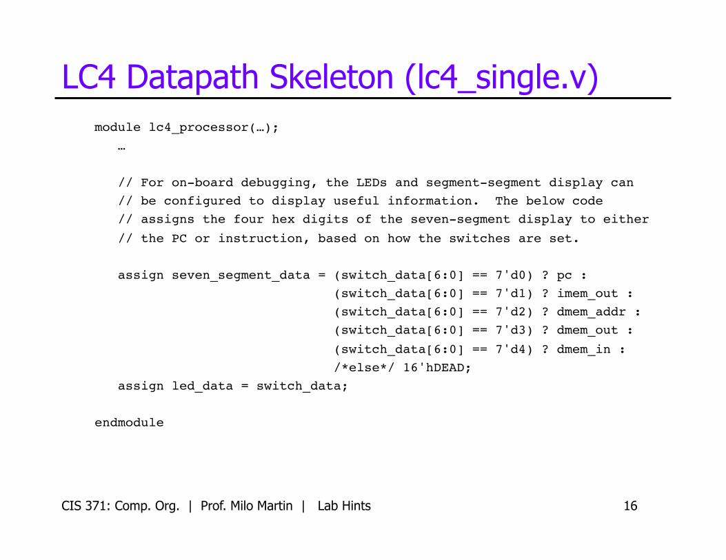
LC4 Datapath Skeleton (lc4_single.v) module lc4_processor(…); ! … !
// For on-board debugging, the LEDs and segment-segment display can! // be configured to display useful information. The below code! // assigns the four hex digits of the seven-segment display to either!
// the PC or instruction, based on how the switches are set.!
assign seven_segment_data = (switch_data[6:0] == 7'd0) ? pc :! (switch_data[6:0] == 7'd1) ? imem_out :! (switch_data[6:0] == 7'd2) ? dmem_addr :! (switch_data[6:0] == 7'd3) ? dmem_out :!
(switch_data[6:0] == 7'd4) ? dmem_in :! /*else*/ 16'hDEAD;! assign led_data = switch_data;!
endmodule!
CIS 371: Comp. Org. | Prof. Milo Martin | Lab Hints 16
Other Verilog & Lab Hints
CIS 371: Comp. Org. | Prof. Milo Martin | Lab Hints 17
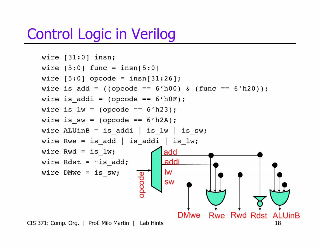
Control Logic in Verilog wire [31:0] insn;!wire [5:0] func = insn[5:0]!wire [5:0] opcode = insn[31:26];!wire is_add = ((opcode == 6’h00) & (func == 6’h20));!wire is_addi = (opcode == 6’h0F);!wire is_lw = (opcode == 6’h23);!wire is_sw = (opcode == 6’h2A);!wire ALUinB = is_addi | is_lw | is_sw; !wire Rwe = is_add | is_addi | is_lw;!wire Rwd = is_lw;!wire Rdst = ~is_add;!wire DMwe = is_sw;!
CIS 371: Comp. Org. | Prof. Milo Martin | Lab Hints 18 ALUinB
opco
de
add addi lw sw
DMwe Rwd Rdst Rwe
CIS 371: Comp. Org. | Prof. Milo Martin | Lab Hints 19
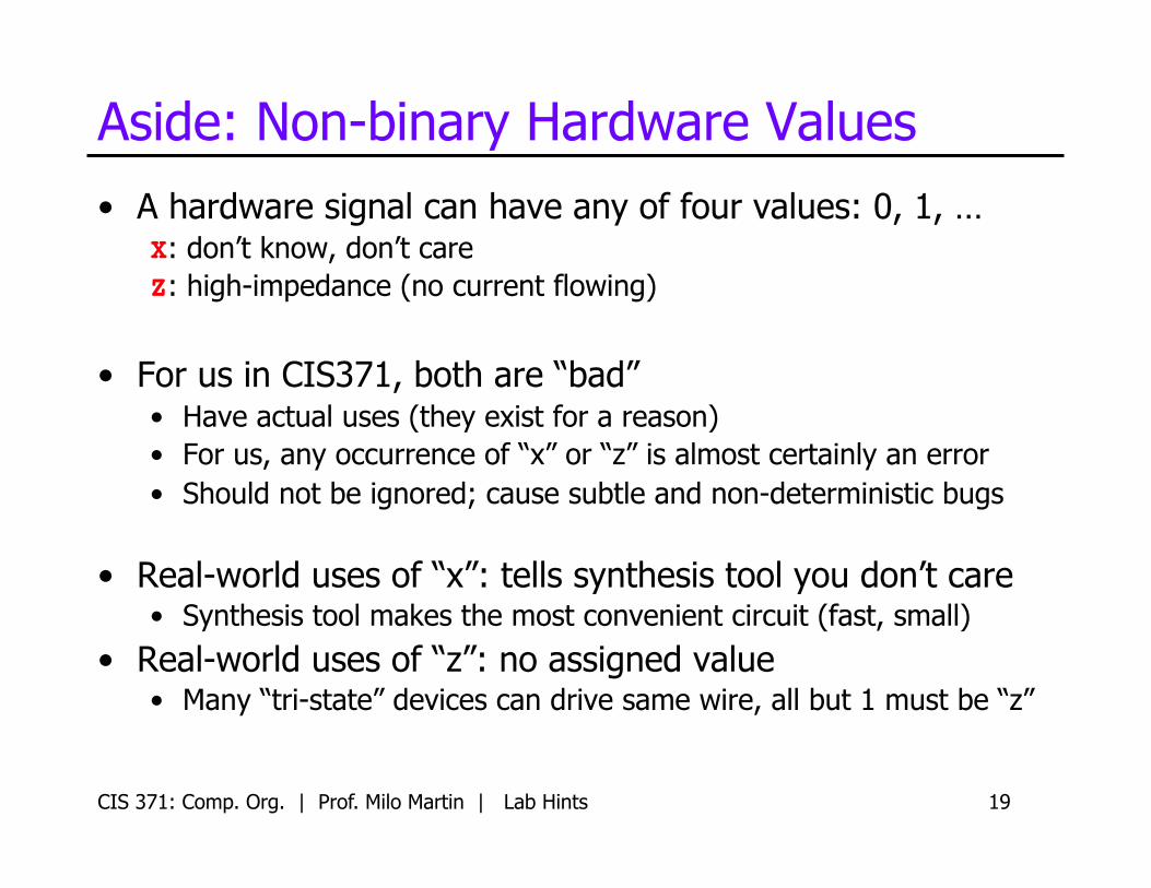
Aside: Non-binary Hardware Values • A hardware signal can have any of four values: 0, 1, …
X: don’t know, don’t care Z: high-impedance (no current flowing)
• For us in CIS371, both are “bad” • Have actual uses (they exist for a reason) • For us, any occurrence of “x” or “z” is almost certainly an error • Should not be ignored; cause subtle and non-deterministic bugs
• Real-world uses of “x”: tells synthesis tool you don’t care • Synthesis tool makes the most convenient circuit (fast, small)
• Real-world uses of “z”: no assigned value • Many “tri-state” devices can drive same wire, all but 1 must be “z”
Testing & Testbenches
CIS 371: Comp. Org. | Prof. Milo Martin | Lab Hints 20
CIS 371: Comp. Org. | Prof. Milo Martin | Lab Hints 21
Testing The Entire Processor
• We give you a testbench module to test the processor
• Instantiates your processor and memory
• Uses a “.trace” file of execution • Uses the “test_” signals to compare to the trace entries
CIS 371: Comp. Org. | Prof. Milo Martin | Lab Hints 22
Testing The Entire Processor
• Need a little bit more to test the entire processor • First thing you need is a program to test • Open file include/bram.v (memory module) • You will see this line at the top
`define MEMORY_IMAGE_FILE "code/wireframe.hex"!
• And these lines inside the memory module reg[15:0] RAM [65535:0]; initial begin! $readmemh(`MEMORY_IMAGE_FILE, RAM, 0, 65535);! end!
• The first line is how you define a memory in verilog • The second is how you define its initial contents
• Xilinx embeds this into the .bit programming file • Change MEMORY_IMAGE_FILE to test different programs
CIS 371: Comp. Org. | Prof. Milo Martin | Lab Hints 23
Creating Test Programs
• We will give you a memory image for (modified) mc • You can use PennSim to create images of smaller programs • First: write a small program in LC4 assembly • Second: assemble using PennSim as command • Third: load into PennSim memory using ld command • Fourth: create memory image using PennSim dump command • Example using file test1.asm!
as test1 test1!ld test1!dump -readmemh 0 xFFFF test1.hex
• Make sure you use the most recent PennSim.jar • Linked from labs
Thoughts on Testing
• You shouldn’t need to modify the testbench
• But feel free to modify it you wish
• However, realize that the sort of “testbench” Verilog is not synthesizable
CIS 371: Comp. Org. | Prof. Milo Martin | Lab Hints 24
Recommended