Complete Product Portfolio
TABLE OF CONTENTS
Introduction .......................................................................................................................... 2
Phototransistor ..................................................................................................................... 5
Isolators - AC Input .............................................................................................................18
Darlington ...........................................................................................................................21
Linear Optocoupler ..............................................................................................................23
High-Speed Optocouplers ..................................................................................................24
Phototriacs ..........................................................................................................................27
Solid-State Relays ..............................................................................................................31
IGBT and MOSFET Drivers .................................................................................................33
Part number Coding ............................................................................................................34
Assembly Instructions .........................................................................................................36
Packaging Information ........................................................................................................40
Packaging Tape and Reel Information.................................................................................42
Product Marking ..................................................................................................................47
Application Examples ..........................................................................................................47
THIS DOCUMENT IS SUBJECT TO CHANGE WITHOUT NOTICE. THE PRODUCTS DESCRIBED HEREIN AND THIS DOCUMENT ARE SUBJECT TO SPECIFIC DISCLAIMERS, SET FORTH AT www.vishay.com/doc?91000
OpTOCOupLErS
V I S H AY I N T E R T E C H N O LO GY, I N C .
BROCHURE TyPE
Discrete Semiconductors and Passive ComponentsOne of the World’s Largest Manufacturers of
VMN-PL0475-1410
Optocoupler product portfolio

Complete Product Portfolio
THIS DOCUMENT IS SUBJECT TO CHANGE WITHOUT NOTICE. THE PRODUCTS DESCRIBED HEREIN AND THIS DOCUMENT ARE SUBJECT TO SPECIFIC DISCLAIMERS, SET FORTH AT www.vishay.com/doc?91000
VMN-PL0475-14102/58BROCHURE TyPE
OpTOCOupLErS
V I S H AY I N T E R T E C H N O LO GY, I N C .
IntroductionIn an electrical circuit, an optocoupler ensures total electric isolation, including potential isolation, as in the case of a transformer. In practice, this means that the control circuit is located on one side of the optocoupler, i.e., the emitter side, while the load circuit is located on the other side, i.e., the detector side. Both circuits are electrically isolated by the optocoupler.
Signals from the control circuit are transmitted optically to the load circuit. In most cases, this optical transmission is realized with light beams whose wavelengths span the red to infrared range, depending on the requirements applicable to the optocoupler. The bandwidth of the signal to be transmitted ranges from a dc voltage signal to frequencies in the MHz band. An optocoupler is comparable to a transformer or relay. Besides having smaller dimensions in most cases, the advantages of optocouplers are shorter switching times, no contact bounce, no interference caused by arcs, and no wear to the circuitry.*
Optocouplers are suitable for circuits used in microelectronics, data processing, and telecommunication systems. Optocouplers are used to an increasing extent as safety tested components, e.g., in switch mode power supplies.
* Note: See Applications Notes for additional information.
DesignAn optocoupler has to fulfill five essential requirements:
• Good isolation
• High current transfer ratio (CTR)
• Low degradation
• Low coupling capacitance
• No interference by field strength influences
These factors are essentially dependent on the design, the materials used, and the corresponding chips used for the emitter/detector.

Complete Product Portfolio
THIS DOCUMENT IS SUBJECT TO CHANGE WITHOUT NOTICE. THE PRODUCTS DESCRIBED HEREIN AND THIS DOCUMENT ARE SUBJECT TO SPECIFIC DISCLAIMERS, SET FORTH AT www.vishay.com/doc?91000
VMN-PL0475-14103/58BROCHURE TyPE
OpTOCOupLErS
V I S H AY I N T E R T E C H N O LO GY, I N C .
ConstructionVishay’s over-under construction optimizes optical transfer efficiency and the need for effective insulation and isolation. The direct optical path from LED and detector optimizes the photon flux on the detector, while providing the highest possible Distance through insulation (DTI). Because of their high DTI most Vishay couplers are rated as “reinforced insulation” by meeting a DTI > 0.4 mm. For those devices that come in packages too small to meet the DTI > 0.4mm, reinforced isolation is achieved through testing.
packages and Functions
Isolation Test Voltage (RMS)Based on Package Type
15.0 kV
11.8 kV
5.3 kV
4.0 kV
3.75 kV
3.0 kV
1.75 kV
17357
Leadframe
Detector die
Bond wire Infrared permeablemold compound
Infrared emitter die
Special moldcompound
17358
Leadframe
Detector die
Bond wireReflected radiance
Clear epoxy compound
Emitter dieEpoxy compound

Complete Product Portfolio
THIS DOCUMENT IS SUBJECT TO CHANGE WITHOUT NOTICE. THE PRODUCTS DESCRIBED HEREIN AND THIS DOCUMENT ARE SUBJECT TO SPECIFIC DISCLAIMERS, SET FORTH AT www.vishay.com/doc?91000
VMN-PL0475-14104/58BROCHURE TyPE
OpTOCOupLErS
V I S H AY I N T E R T E C H N O LO GY, I N C .
Optocoupler Structure
Phototransistor
DC-Input AC-Input
Photo-Darlington
DC-Input AC-Input
High-Speed
Analog
Photodiode-transistor Dual Channel
Digital
OC-Output Totem Pole Output
Linear Photodiode
phototriac
Phototriac
Non Zero-crossing Zero-crossing
PowerPhototriac
SSR (photo-MOSFET)
Form A (normally open)
Form B (normally close)
Form A/B, C
IGBT / MOSFET Driver
IGBT MOSFET Driver (photo-voltaic)
Telecom Switch
K2K1
Shield
*Zero crossing circuit
ZCC*
TurnOff
Complete Product Portfolio
THIS DOCUMENT IS SUBJECT TO CHANGE WITHOUT NOTICE. THE PRODUCTS DESCRIBED HEREIN AND THIS DOCUMENT ARE SUBJECT TO SPECIFIC DISCLAIMERS, SET FORTH AT www.vishay.com/doc?91000
VMN-PL0475-14105/58BROCHURE TyPE
OpTOCOupLErS
V I S H AY I N T E R T E C H N O LO GY, I N C .
Optocouplers / Isolators - phototransistor Output
phototransistor
SSOp-4 SOp-4 SOIC-8 DIp-4 LSOp-4 DIp-6 DIp-8 (2-ch)
DIp-16 (4-ch)
HV-DIp
VISO 3750 VRMS 4000 VRMS 5300 VrMS 8200 VRMS
DC input1 mA VOS618A VOM618A
VO20xx, VOD20x (2), VOD21x (2)
VO618A VOL618A - - -
5 mA VOS617A VOM617A VO617AVOL617A, TCLT1100
CNy17, CNy17F
ILD621 ILQ621 -
10 mA VOS615A -VO615A, VO610A
TCLT1100 (5-pin)
ILD615ILQ1/2/5, ILQ615
CNy64(A), CNy65(A), CNy66(A), CNy65Exi
Features
• Isolation test voltage up to 7900 VRMS
• Extensive CTR (current transfer ratio) ranges from 40 % to 600 %
• Low input drive current down to 1 mA
• Certified to UL, CSA, VDE, Fimko, and CQC safety standards
• RoHS-compliant, lead (Pb)-free, and eco-friendly “green” compound
>>>
phototransistor Base part
Numberpackage
Forward Current
IF
part NumberCTr min (%)
CTr max (%)
VCEO (V)
Forward Current IF max. (mA)
Operating Temperature
max. (°C)
Isolation Voltage
VISO (VrMS)
Ch(s)Creepage distance
(mm)Safety Standard(s)
VO610A
DIP-4 10 mA VO610A-1 40 80 70 60 –55 to +110 5000 1 ≥7BSI, VDE, FIMKO, UL, cUL,
CQC
DIP-4 10 mA VO610A-2 63 125 70 60 –55 to +110 5000 1 ≥7BSI, VDE, FIMKO, UL, cUL,
CQC
DIP-4 10 mA VO610A-3 100 200 70 60 –55 to +110 5000 1 ≥7BSI, VDE, FIMKO, UL, cUL,
CQC
DIP-4 10 mA VO610A-4 160 320 70 60 –55 to +110 5000 1 ≥7BSI, VDE, FIMKO, UL, cUL,
CQC
Applications
• Switch mode power supply (SMPS)
• Home appliances
• Telecommunication
• Industrial control and automation
resources
• Phototransistor Output www.vishay.com/optocouplers/opt-tran-output/
Complete Product Portfolio
THIS DOCUMENT IS SUBJECT TO CHANGE WITHOUT NOTICE. THE PRODUCTS DESCRIBED HEREIN AND THIS DOCUMENT ARE SUBJECT TO SPECIFIC DISCLAIMERS, SET FORTH AT www.vishay.com/doc?91000
VMN-PL0475-14106/58BROCHURE TyPE
OpTOCOupLErS
V I S H AY I N T E R T E C H N O LO GY, I N C .
Base part
Numberpackage
Forward Current
IF
part NumberCTr min (%)
CTr max (%)
VCEO (V)
Forward Current IF max. (mA)
Operating Temperature
max. (°C)
Isolation Voltage
VISO (VrMS)
Ch(s)Creepage distance
(mm)Safety Standard(s)
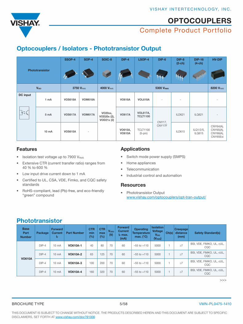
VO615A
DIP-4 5 mA VO615A 50 600 70 60 –55 to +110 5000 1 ≥7; ≥8BSI, VDE, FIMKO, UL, cUL,
CQC
DIP-4 10 mA VO615A-1 40 80 70 60 –55 to +110 5000 1 ≥7; ≥8BSI, VDE, FIMKO, UL, cUL,
CQC
DIP-4 10 mA VO615A-2 63 125 70 60 –55 to +110 5000 1 ≥7; ≥8BSI, VDE, FIMKO, UL, cUL,
CQC
DIP-4 10 mA VO615A-3 100 200 70 60 –55 to +110 5000 1 ≥7; ≥8BSI, VDE, FIMKO, UL, cUL,
CQC
DIP-4 10 mA VO615A-4 160 320 70 60 –55 to +110 5000 1 ≥7; ≥8BSI, VDE, FIMKO, UL, cUL,
CQC
DIP-4 5 mA VO615A-5 50 150 70 60 –55 to +110 5000 1 ≥7; ≥8BSI, VDE, FIMKO, UL, cUL,
CQC
DIP-4 5 mA VO615A-6 100 300 70 60 –55 to +110 5000 1 ≥7; ≥8BSI, VDE, FIMKO, UL, cUL,
CQC
DIP-4 5 mA VO615A-7 80 160 70 60 –55 to +110 5000 1 ≥7; ≥8BSI, VDE, FIMKO, UL, cUL,
CQC
DIP-4 5 mA VO615A-8 130 260 70 60 –55 to +110 5000 1 ≥7; ≥8BSI, VDE, FIMKO, UL, cUL,
CQC
DIP-4 5 mA VO615A-9 200 400 70 60 –55 to +110 5000 1 ≥7; ≥8BSI, VDE, FIMKO, UL, cUL,
CQC
TCET1200
DIP-4 5 mA TCET1200 50 600 70 60 –40 to +100 5000 1 ≥7 BSI, VDE, FIMKO, UL, cUL
DIP-4 10 mA TCET1201 40 80 70 60 –40 to +100 5000 1 ≥7 BSI, VDE, FIMKO, UL, cUL
DIP-4 10 mA TCET1202 63 125 70 60 –40 to +100 5000 1 ≥7 BSI, VDE, FIMKO, UL, cUL
DIP-4 10 mA TCET1203 100 200 70 60 –40 to +100 5000 1 ≥7 BSI, VDE, FIMKO, UL, cUL
DIP-4 10 mA TCET1204 160 320 70 60 –40 to +100 5000 1 ≥7 BSI, VDE, FIMKO, UL, cUL
VO617A
DIP-4 5 mA VO617A 40 600 80 60 –55 to +110 5300 1 ≥7; ≥8UL, cUL, VDE, BSI, FIMKO,
CQC
DIP-4 5 mA VO617A-1 40 80 80 60 –55 to +110 5300 1 ≥7; ≥8UL, cUL, VDE, BSI, FIMKO,
CQC
DIP-4 5 mA VO617A-2 63 125 80 60 –55 to +110 5300 1 ≥7; ≥8UL, cUL, VDE, BSI, FIMKO,
CQC
DIP-4 5 mA VO617A-3 100 200 80 60 –55 to +110 5300 1 ≥7; ≥8UL, cUL, VDE, BSI, FIMKO,
CQC
DIP-4 5 mA VO617A-4 160 320 80 60 –55 to +110 5300 1 ≥7; ≥8UL, cUL, VDE, BSI, FIMKO,
CQC
DIP-4 5 mA VO617A-7 80 160 80 60 –55 to +110 5300 1 ≥7; ≥8UL, cUL, VDE, BSI, FIMKO,
CQC
DIP-4 5 mA VO617A-8 130 260 80 60 –55 to +110 5300 1 ≥7; ≥8UL, cUL, VDE, BSI, FIMKO,
CQC
VO618A
DIP-4 1 mA VO618A 50 600 80 60 –55 to +110 5300 1 ≥7; ≥8UL, cUL, VDE, BSI, FIMKO,
CQC
DIP-4 1 mA VO618A-2 63 125 80 60 –55 to +110 5300 1 ≥7; ≥8UL, cUL, VDE, BSI, FIMKO,
CQC
DIP-4 1 mA VO618A-3 100 200 80 60 –55 to +110 5300 1 ≥7; ≥8UL, cUL, VDE, BSI, FIMKO,
CQC
DIP-4 1 mA VO618A-4 160 320 80 60 –55 to +110 5300 1 ≥7; ≥8UL, cUL, VDE, BSI, FIMKO,
CQC
>>>
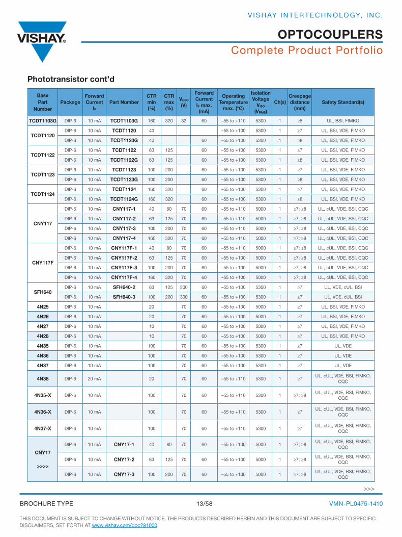
phototransistor cont’d

Complete Product Portfolio
THIS DOCUMENT IS SUBJECT TO CHANGE WITHOUT NOTICE. THE PRODUCTS DESCRIBED HEREIN AND THIS DOCUMENT ARE SUBJECT TO SPECIFIC DISCLAIMERS, SET FORTH AT www.vishay.com/doc?91000
VMN-PL0475-14107/58BROCHURE TyPE
OpTOCOupLErS
V I S H AY I N T E R T E C H N O LO GY, I N C .
Base part
Numberpackage
Forward Current
IF
part NumberCTr min (%)
CTr max (%)
VCEO (V)
Forward Current IF max. (mA)
Operating Temperature
max. (°C)
Isolation Voltage
VISO (VrMS)
Ch(s)Creepage distance
(mm)Safety Standard(s)
SFH1617A
DIP-4 10 mA SFH1617A-1 40 80 70 60 –55 to +150 5300 1 ≥7; ≥8 UL, BSI, cUL, VDE
DIP-4 10 mA SFH1617A-2 63 125 70 60 –55 to +150 5300 1 ≥7; ≥8 UL, BSI, cUL, VDE
DIP-4 10 mA SFH1617A-3 100 200 70 60 –55 to +150 5300 1 ≥7; ≥8 UL, BSI, cUL, VDE
DIP-4 10 mA SFH1617A-4 160 320 70 60 –55 to +150 5300 1 ≥7; ≥8 UL, BSI, cUL, VDE
SFH610A
DIP-4 10 mA SFH610A-1 40 80 70 60 –55 to +100 5300 1 ≥7 UL, BSI, cUL, VDE
DIP-4 10 mA SFH610A-2 63 125 70 60 –55 to +100 5300 1 ≥7 UL, BSI, cUL, VDE
DIP-4 10 mA SFH610A-3 100 200 70 60 –55 to +100 5300 1 ≥7 UL, BSI, cUL, VDE
DIP-4 10 mA SFH610A-4 160 320 70 60 –55 to +100 5300 1 ≥7 UL, BSI, cUL, VDE
DIP-4 10 mA SFH610A-5 250 500 70 60 –55 to +100 5300 1 ≥7 UL, BSI, cUL, VDE
SFH615A
DIP-4 10 mA SFH615A-1 40 80 70 60 –55 to +100 5300 1 ≥7; ≥8 UL, cUL, BSI, FIMKO, VDE
DIP-4 10 mA SFH615A-2 63 125 70 60 –55 to +100 5300 1 ≥7; ≥8 UL, VDE
DIP-4 10 mA SFH615A-3 100 200 70 60 –55 to +100 5300 1 ≥7; ≥8 UL, VDE
DIP-4 10 mA SFH615A-4 160 320 70 60 –55 to +100 5300 1 ≥7; ≥8 UL, VDE
SFH615
DIP-4 10 mA SFH615AA 50 600 70 60 –55 to +100 5300 1 ≥7; ≥8 UL, BSI, VDE
DIP-4 10 mA SFH615AB 80 260 70 60 –55 to +100 5300 1 ≥7; ≥8 UL, BSI, VDE
DIP-4 10 mA SFH615ABL 200 600 70 60 –55 to +100 5300 1 ≥7; ≥8 UL, BSI, VDE
DIP-4 10 mA SFH615ABM 200 400 70 60 –55 to +100 5300 1 ≥7; ≥8 UL, BSI, VDE
DIP-4 10 mA SFH615AGB 100 600 70 60 –55 to +100 5300 1 ≥7; ≥8 UL, BSI, VDE
DIP-4 10 mA SFH615AGr 100 300 70 60 –55 to +100 5300 1 ≥7; ≥8 UL, BSI, VDE
DIP-4 10 mA SFH615AY 50 150 70 60 –55 to +100 5300 1 ≥7; ≥8 UL, BSI, VDE
SFH617A
DIP-4 10 mA SFH617A-1 40 80 70 60 –55 to +110 5300 1 ≥7 UL, BSI, cUL, VDE, FIMKO
DIP-4 10 mA SFH617A-2 63 125 70 60 –55 to +110 5300 1 ≥7 UL, BSI, cUL, VDE, FIMKO
DIP-4 10 mA SFH617A-3 100 200 70 60 –55 to +110 5300 1 ≥7 UL, BSI, cUL, VDE, FIMKO
DIP-4 10 mA SFH617A-4 160 320 70 60 –55 to +110 5300 1 ≥7 UL, BSI, cUL, VDE, FIMKO
SFH618A
DIP-4 1 mA SFH618A-2 63 125 55 60 –55 to +100 5300 1 ≥7; ≥8 UL, BSI, cUL, VDE, FIMKO
DIP-4 1 mA SFH618A-3 100 200 55 60 –55 to +100 5300 1 ≥7; ≥8 UL, BSI, cUL, VDE, FIMKO
DIP-4 1 mA SFH618A-4 160 320 55 60 –55 to +100 5300 1 ≥7; ≥8 UL, BSI, cUL, VDE, FIMKO
DIP-4 1 mA SFH618A-5 250 500 55 60 –55 to +100 5300 1 ≥7; ≥8 UL, BSI, cUL, VDE, FIMKO
TCED1100 DIP-4 1 mA TCED1100 600 35 60 –55 to +100 5300 1 ≥7; ≥8 UL, BSI, cUL, FIMKO
TCED1100G DIP-4 1 mA TCED1100G 600 35 60 –55 to +100 5300 1 ≥7; ≥8 UL, BSI, cUL, FIMKO
TCET1100 DIP-4 5 mA TCET1100 50 600 70 60 –55 to +100 5000 1 ≥7; ≥8 UL, BSI, VDE, FIMKO
TCET1101 DIP-4 10 mA TCET1101 40 80 70 60 –55 to +100 5000 1 ≥7; ≥8 UL, BSI, VDE, FIMKO
TCET1102 DIP-4 10 mA TCET1102 63 125 70 60 –55 to +100 5000 1 ≥7; ≥8 UL, BSI, VDE, FIMKO
TCET1103 DIP-4 10 mA TCET1103 100 200 70 60 –55 to +100 5000 1 ≥7; ≥8 UL, BSI, VDE, FIMKO
TCET1104 DIP-4 10 mA TCET1104 160 320 70 60 –55 to +100 5000 1 ≥7; ≥8 UL, BSI, VDE, FIMKO
TCET1105 DIP-4 10 mA TCET1105 50 150 70 60 –55 to +100 5000 1 ≥7; ≥8 UL, BSI, VDE, FIMKO
TCET1106 DIP-4 5 mA TCET1106 100 300 70 60 –55 to +100 5000 1 ≥7; ≥8 UL, BSI, VDE, FIMKO
TCET1107 DIP-4 5 mA TCET1107 80 160 70 60 –55 to +100 5000 1 ≥7; ≥8 UL, BSI, VDE, FIMKO
TCET1108 DIP-4 5 mA TCET1108 130 260 70 60 –55 to +100 5000 1 ≥7; ≥8 UL, BSI, VDE, FIMKO
>>>
phototransistor cont’d

Complete Product Portfolio
THIS DOCUMENT IS SUBJECT TO CHANGE WITHOUT NOTICE. THE PRODUCTS DESCRIBED HEREIN AND THIS DOCUMENT ARE SUBJECT TO SPECIFIC DISCLAIMERS, SET FORTH AT www.vishay.com/doc?91000
VMN-PL0475-14108/58BROCHURE TyPE
OpTOCOupLErS
V I S H AY I N T E R T E C H N O LO GY, I N C .
phototransistor cont’d
Base part
Numberpackage
Forward Current
IF
part NumberCTr min (%)
CTr max (%)
VCEO (V)
Forward Current IF max. (mA)
Operating Temperature
max. (°C)
Isolation Voltage
VISO (VrMS)
Ch(s)Creepage distance
(mm)Safety Standard(s)
TCET1109 DIP-4 5 mA TCET1109 200 400 70 60 –55 to +100 5000 1 ≥7; ≥8 UL, BSI, VDE, FIMKO
TCET1100G DIP-4 5 mA TCET1100G 50 600 70 60 –55 to +100 5000 1 ≥7; ≥8 UL, BSI, VDE, FIMKO
TCET1101G DIP-4 10 mA TCET1101G 40 80 70 60 –55 to +100 5000 1 ≥7; ≥8 UL, BSI, VDE, FIMKO
TCET1102G DIP-4 10 mA TCET1102G 63 125 70 60 –55 to +100 5000 1 ≥7; ≥8 UL, BSI, VDE, FIMKO
TCET1103G DIP-4 10 mA TCET1103G 100 200 70 60 –55 to +100 5000 1 ≥7; ≥8 UL, BSI, VDE, FIMKO
TCET1104G DIP-4 10 mA TCET1104G 160 320 70 60 –55 to +100 5000 1 ≥7; ≥8 UL, BSI, VDE, FIMKO
TCET1105G DIP-4 10 mA TCET1105G 50 150 70 60 –55 to +100 5000 1 ≥7; ≥8 UL, BSI, VDE, FIMKO
TCET1106G DIP-4 5 mA TCET1106G 100 300 70 60 –55 to +100 5000 1 ≥7; ≥8 UL, BSI, VDE, FIMKO
TCET1107G DIP-4 5 mA TCET1107G 80 160 70 60 –55 to +100 5000 1 ≥7; ≥8 UL, BSI, VDE, FIMKO
TCET1108G DIP-4 5 mA TCET1108G 130 260 70 60 –55 to +100 5000 1 ≥7; ≥8 UL, BSI, VDE, FIMKO
TCET1109G DIP-4 5 mA TCET1109G 200 400 70 60 –55 to +100 5000 1 ≥7; ≥8 UL, BSI, VDE, FIMKO
TCET1110
DIP-4 5 mA TCET1100 50 600 70 60 –40 to +110 5000 1 ≥7; ≥8 UL, BSI, VDE, FIMKO
DIP-4 10 mA TCET1102 63 125 70 60 –40 to +110 5000 1 ≥7; ≥8 UL, BSI, VDE, FIMKO
DIP-4 10 mA TCET1103 100 200 70 60 –40 to +110 5000 1 ≥7; ≥8 UL, BSI, VDE, FIMKO
DIP-4 10 mA TCET1104 160 320 70 60 –40 to +110 5000 1 ≥7; ≥8 UL, BSI, VDE, FIMKO
DIP-4 5 mA TCET1100G 50 600 70 60 –40 to +110 5000 1 ≥7; ≥8 UL, BSI, VDE, FIMKO
DIP-4 10 mA TCET1102G 63 125 70 60 –40 to +110 5000 1 ≥7; ≥8 UL, BSI, VDE, FIMKO
DIP-4 10 mA TCET1103G 100 200 70 60 –40 to +110 5000 1 ≥7; ≥8 UL, BSI, VDE, FIMKO
DIP-4 10 mA TCET1104G 160 320 70 60 –40 to +110 5000 1 ≥7; ≥8 UL, BSI, VDE, FIMKO
VO615C
DIP-4 10 mA VO615C-1 40 80 70 60 –55 to +110 5000 1BSI, VDE, FIMKO, UL, cUL,
CQC
DIP-4 10 mA VO615C-2 63 125 70 60 –55 to +110 5000 1BSI, VDE, FIMKO, UL, cUL,
CQC
DIP-4 10 mA VO615C-3 100 200 70 60 –55 to +110 5000 1BSI, VDE, FIMKO, UL, cUL,
CQC
DIP-4 10 mA VO615C-4 160 320 70 60 –55 to +110 5000 1BSI, VDE, FIMKO, UL, cUL,
CQC
VO617C
DIP-4 5 mA VO617C-1 40 80 70 60 –55 to +110 5000 1BSI, VDE, FIMKO, UL, cUL,
CQC
DIP-4 5 mA VO617C-2 63 125 70 60 –55 to +110 5000 1BSI, VDE, FIMKO, UL, cUL,
CQC
DIP-4 5 mA VO617C-3 100 200 70 60 –55 to +110 5000 1BSI, VDE, FIMKO, UL, cUL,
CQC
DIP-4 5 mA VO617C-4 160 320 70 60 –55 to +110 5000 1BSI, VDE, FIMKO, UL, cUL,
CQC
CNY65ExiDIP-4 HV 10 mA CNY65Exi 50 300 32 75 –55 to +85 11600 1 ATEX
DIP-4 HV 10 mA CNY65BExi 100 200 32 75 –55 to +85 11600 1 ATEX
CNY64
DIP-4 HV 10 mA CNY64 50 300 32 75 –55 to +85 8200 1 UL, VDE
DIP-4 HV 10 mA CNY64A 50 300 32 75 –55 to +85 8200 1 UL, VDE
DIP-4 HV 10 mA CNY64B 50 300 32 75 –55 to +85 8200 1 UL, VDE
CNY65
DIP-4 HV 10 mA CNY65 63 125 32 75 –55 to +85 8200 1 UL, VDE
DIP-4 HV 10 mA CNY65A 63 125 32 75 –55 to +85 8200 1 UL, VDE
DIP-4 HV 10 mA CNY65B 63 125 32 75 –55 to +85 8200 1 UL, VDE
>>>
Complete Product Portfolio
THIS DOCUMENT IS SUBJECT TO CHANGE WITHOUT NOTICE. THE PRODUCTS DESCRIBED HEREIN AND THIS DOCUMENT ARE SUBJECT TO SPECIFIC DISCLAIMERS, SET FORTH AT www.vishay.com/doc?91000
VMN-PL0475-14109/58BROCHURE TyPE
OpTOCOupLErS
V I S H AY I N T E R T E C H N O LO GY, I N C .
>>>
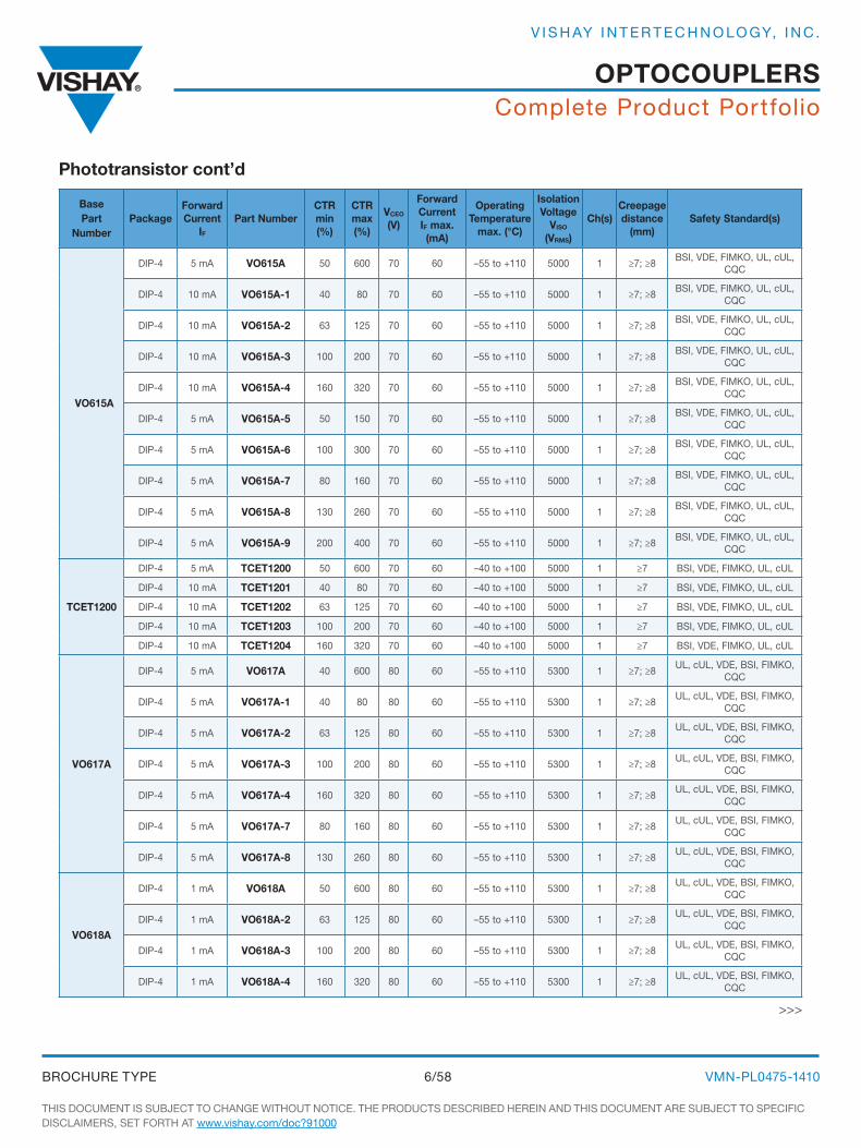
phototransistor cont’d
Base part
Numberpackage
Forward Current
IF
part NumberCTr min (%)
CTr max (%)
VCEO (V)
Forward Current IF max. (mA)
Operating Temperature
max. (°C)
Isolation Voltage
VISO (VrMS)
Ch(s)Creepage distance
(mm)Safety Standard(s)
CNY651 DIP-4 HV 5 mA CNY651AGr 100 300 32 75 –55 to +85 8200 1 UL, cUL, VDE
CNY66DIP-4 HV 10 mA CNY66 100 200 32 75 –55 to +85 8200 1 UL, VDE
DIP-4 HV 10 mA CNY66B 100 200 32 75 –55 to +85 8200 1 UL, VDE
CNY64S SMD-4 HV 5 mA CNY64ST 50 300 32 75 –55 to +85 8200 1 UL, cUL, VDE
CNY64S SMD-4 HV 5 mA CNY64AYST 50 150 32 75 –55 to +85 8200 1 UL, cUL, VDE
CNY64S SMD-4 HV 5 mA CNY64ABST 80 240 32 75 –55 to +85 8200 1 UL, cUL, VDE
CNY64S SMD-4 HV 5 mA CNY64AGrST 100 300 32 75 –55 to +85 8200 1 UL, cUL, VDE
CNY65S SMD-4 HV 5 mA CNY65ST 50 300 32 75 –55 to +85 8200 1 UL, cUL, VDE
CNY65S SMD-4 HV 5 mA CNY65AYST 50 150 32 75 –55 to +85 8200 1 UL, cUL, VDE
CNY65S SMD-4 HV 5 mA CNY65ABST 80 240 32 75 –55 to +85 8200 1 UL, cUL, VDE
CNY65S SMD-4 HV 5 mA CNY65AGrST 100 300 32 75 –55 to +85 8200 1 UL, cUL, VDE
CNY651 SMD-4 HV 5 mA CNY651AYST 50 150 32 75 –40 to +110 8200 1 UL, cUL, VDE
CNY651 SMD-4 HV 5 mA CNY651AGrST 100 300 32 75 –40 to +110 8200 1 UL, cUL, VDE
SFH6106
SMD-4 10 mA SFH6106-1 40 80 70 60 –55 to +100 5300 1 ≥7; ≥8 UL, BSI, cUL, VDE
SMD-4 10 mA SFH6106-2 63 125 70 60 –55 to +100 5300 1 ≥7; ≥8 UL, BSI, cUL, VDE
SMD-4 10 mA SFH6106-3 100 200 70 60 –55 to +100 5300 1 ≥7; ≥8 UL, BSI, cUL, VDE
SMD-4 10 mA SFH6106-4 160 320 70 60 –55 to +100 5300 1 ≥7; ≥8 UL, BSI, cUL, VDE
SMD-4 10 mA SFH6106-5 250 500 70 60 –55 to +100 5300 1 ≥7; ≥8 UL, BSI, cUL, VDE
SFH6156
SMD-4 10 mA SFH6156-1 40 80 70 60 –55 to +100 5300 1 ≥7UL, BSI, cUL, VDE, FIMKO,
CQC
SMD-4 10 mA SFH6156-2 63 125 70 60 –55 to +100 5300 1 ≥7UL, BSI, cUL, VDE, FIMKO,
CQC
SMD-4 10 mA SFH6156-3 100 200 70 60 –55 to +100 5300 1 ≥7UL, BSI, cUL, VDE, FIMKO,
CQC
SMD-4 10 mA SFH6156-4 160 320 70 60 –55 to +100 5300 1 ≥7UL, BSI, cUL, VDE, FIMKO,
CQC
SFH6186
SMD-4 1 mA SFH6186-2 63 125 55 60 –55 to +100 5300 1 ≥7 UL, BSI, cUL, VDE, FIMKO
SMD-4 1 mA SFH6186-3 100 200 55 60 –55 to +100 5300 1 ≥7 UL, BSI, cUL, VDE, FIMKO
SMD-4 1 mA SFH6186-4 160 320 55 60 –55 to +100 5300 1 ≥7 UL, BSI, cUL, VDE, FIMKO
SMD-4 1 mA SFH6186-5 250 500 55 60 –55 to +100 5300 1 ≥7 UL, BSI, cUL, VDE, FIMKO
TCMT110 SMD-4 5 mA TCMT1110 50 600 70 50 –45 to +110 3750 1 ≥5 UL, BSI, cUL, VDE
TCMT1111 SMD-4 5 mA TCMT1111 40 80 70 50 –45 to +110 3750 1 ≥5 UL, BSI, cUL, VDE
TCMT1112 SMD-4 10 mA TCMT1112 63 125 70 50 –45 to +110 3750 1 ≥5 UL, BSI, cUL, VDE
TCMT1113 SMD-4 10 mA TCMT1113 100 200 70 50 –45 to +110 3750 1 ≥5 UL, BSI, cUL, VDE
TCMT1114 SMD-4 10 mA TCMT1114 160 320 70 50 –45 to +110 3750 1 ≥5 UL, BSI, cUL, VDE
TCMT1115 SMD-4 10 mA TCMT1115 50 150 70 50 –45 to +110 3750 1 ≥5 UL, BSI, cUL, VDE
TCMT1116 SMD-4 10 mA TCMT1116 100 300 70 50 –45 to +110 3750 1 ≥5 UL, BSI, cUL, VDE
TCMT1117 SMD-4 5 mA TCMT1117 80 160 70 50 –45 to +110 3750 1 ≥5 UL, BSI, cUL, VDE
TCMT1118 SMD-4 5 mA TCMT1118 130 260 70 50 –45 to +110 3750 1 ≥5 UL, BSI, cUL, VDE
TCMT1119 SMD-4 5 mA TCMT1119 200 400 70 50 –45 to +110 3750 1 ≥5 UL, BSI, cUL, VDE

Complete Product Portfolio
THIS DOCUMENT IS SUBJECT TO CHANGE WITHOUT NOTICE. THE PRODUCTS DESCRIBED HEREIN AND THIS DOCUMENT ARE SUBJECT TO SPECIFIC DISCLAIMERS, SET FORTH AT www.vishay.com/doc?91000
VMN-PL0475-141010/58BROCHURE TyPE
OpTOCOupLErS
V I S H AY I N T E R T E C H N O LO GY, I N C .
>>>
phototransistor cont’d
Base part
Numberpackage
Forward Current
IF
part NumberCTr min (%)
CTr max (%)
VCEO (V)
Forward Current IF max. (mA)
Operating Temperature
max. (°C)
Isolation Voltage
VISO (VrMS)
Ch(s)Creepage distance
(mm)Safety Standard(s)
VOM618A
SOP-4 1 mA VOM618A 50 600 80 60 –55 to +110 3750 1 ≥5 UL, cUL, VDE, FIMKO, CQC
SOP-4 1 mA VOM618A-1 40 80 80 60 –55 to +110 3750 1 ≥5 UL, cUL, VDE, FIMKO, CQC
SOP-4 1 mA VOM618A-2 63 125 80 60 –55 to +110 3750 1 ≥5 UL, cUL, VDE, FIMKO, CQC
SOP-4 1 mA VOM618A-3 100 200 80 60 –55 to +110 3750 1 ≥5 UL, cUL, VDE, FIMKO, CQC
SOP-4 1 mA VOM618A-4 160 320 80 60 –55 to +110 3750 1 ≥5 UL, cUL, VDE, FIMKO, CQC
SOP-4 1 mA VOM618A-5 50 100 80 60 –55 to +110 3750 1 ≥5 UL, cUL, VDE, FIMKO, CQC
SOP-4 1 mA VOM618A-7 80 160 80 60 –55 to +110 3750 1 ≥5 UL, cUL, VDE, FIMKO, CQC
SOP-4 1 mA VOM618A-8 130 260 80 60 –55 to +110 3750 1 ≥5 UL, cUL, VDE, FIMKO, CQC
VOM617A
SOP-4 5 mA VOM617A 50 600 80 60 –55 to +110 3750 1 ≥5 UL, cUL, VDE, FIMKO, CQC
SOP-4 5 mA VOM617A-2 63 125 80 60 –55 to +110 3750 1 ≥5 UL, cUL, VDE, FIMKO, CQC
SOP-4 5 mA VOM617A-3 100 200 80 60 –55 to +110 3750 1 ≥5 UL, cUL, VDE, FIMKO, CQC
SOP-4 5 mA VOM617A-4 160 320 80 60 –55 to +110 3750 1 ≥5 UL, cUL, VDE, FIMKO, CQC
SOP-4 5 mA VOM617A-6 250 500 80 60 –55 to +110 3750 1 ≥5 UL, cUL, VDE, FIMKO, CQC
SOP-4 5 mA VOM617A-7 80 160 80 60 –55 to +110 3750 1 ≥5 UL, cUL, VDE, FIMKO, CQC
SOP-4 5 mA VOM617A-8 130 260 80 60 –55 to +110 3750 1 ≥5 UL, cUL, VDE, FIMKO, CQC
SOP-4 5 mA VOM617A-9 200 400 80 60 –55 to +110 3750 1 ≥5 UL, cUL, VDE, FIMKO, CQC
VOS615A
SSOP-4 10 mA VOS615A 50 600 80 50 –55 to +110 3750 1 ≥5 UL, cUL, VDE, FIMKO, CQC
SSOP-4 10 mA VOS615A-1 40 80 80 50 –55 to +110 3750 1 ≥5 UL, cUL, VDE, FIMKO, CQC
SSOP-4 10 mA VOS615A-2 63 125 80 50 –55 to +110 3750 1 ≥5 UL, cUL, VDE, FIMKO, CQC
SSOP-4 10 mA VOS615A-3 100 200 80 50 –55 to +110 3750 1 ≥5 UL, cUL, VDE, FIMKO, CQC
SSOP-4 10 mA VOS615A-4 160 320 80 50 –55 to +110 3750 1 ≥5 UL, cUL, VDE, FIMKO, CQC
VOS617A
SSOP-4 5 mA VOS617A 50 600 80 50 –55 to +110 3750 1 ≥5 UL, cUL, VDE, FIMKO, CQC
SSOP-4 5 mA VOS617A-2 63 125 80 50 –55 to +110 3750 1 ≥5 UL, cUL, VDE, FIMKO, CQC
SSOP-4 5 mA VOS617A-3 100 200 80 50 –55 to +110 3750 1 ≥5 UL, cUL, VDE, FIMKO, CQC
SSOP-4 5 mA VOS617A-4 160 320 80 50 –55 to +110 3750 1 ≥5 UL, cUL, VDE, FIMKO, CQC
SSOP-4 5 mA VOS617A-7 80 160 80 50 –55 to +110 3750 1 ≥5 UL, cUL, VDE, FIMKO, CQC
SSOP-4 5 mA VOS617A-8 130 260 80 50 –55 to +110 3750 1 ≥5 UL, cUL, VDE, FIMKO, CQC
SSOP-4 5 mA VOS617A-9 200 400 80 50 –55 to +110 3750 1 ≥5 UL, cUL, VDE, FIMKO, CQC
VOS618A
SSOP-4 1 mA VOS618A 50 600 80 50 –55 to +110 3750 1 ≥5 UL, cUL, VDE, FIMKO, CQC
SSOP-4 1 mA VOS618A-2 63 125 80 50 –55 to +110 3750 1 ≥5 UL, cUL, VDE, FIMKO, CQC
SSOP-4 1 mA VOS618A-3 100 200 80 50 –55 to +110 3750 1 ≥5 UL, cUL, VDE, FIMKO, CQC
SSOP-4 1 mA VOS618A-7 80 160 80 50 –55 to +110 3750 1 ≥5 UL, cUL, VDE, FIMKO, CQC
SSOP-4 1 mA VOS618A-8 130 260 80 50 –55 to +110 3750 1 ≥5 UL, cUL, VDE, FIMKO, CQC
VOL617A
>>>>
LSOP-4 5 mA VOL617A-1 40 80 80 60 –55 to +110 5000 1 ≥5UL, cUL, VDE, BSI, FIMKO,
CQC
LSOP-4 5 mA VOL617A-2 63 125 80 60 –55 to +110 5000 1 ≥5UL, cUL, VDE, BSI, FIMKO,
CQC
LSOP-4 5 mA VOL617A-3 100 200 80 60 –55 to +110 5000 1 ≥5UL, cUL, VDE, BSI, FIMKO,
CQC
LSOP-4 5 mA VOL617A-4 160 320 80 60 –55 to +110 5000 1 ≥5UL, cUL, VDE, BSI, FIMKO,
CQC

Complete Product Portfolio
THIS DOCUMENT IS SUBJECT TO CHANGE WITHOUT NOTICE. THE PRODUCTS DESCRIBED HEREIN AND THIS DOCUMENT ARE SUBJECT TO SPECIFIC DISCLAIMERS, SET FORTH AT www.vishay.com/doc?91000
VMN-PL0475-141011/58BROCHURE TyPE
OpTOCOupLErS
V I S H AY I N T E R T E C H N O LO GY, I N C .
>>>
phototransistor cont’d
Base part
Numberpackage
Forward Current
IF
part NumberCTr min (%)
CTr max (%)
VCEO (V)
Forward Current IF max. (mA)
Operating Temperature
max. (°C)
Isolation Voltage
VISO (VrMS)
Ch(s)Creepage distance
(mm)Safety Standard(s)
VOL617A (cont)
LSOP-4 5 mA VOL617A-8 130 260 80 60 –55 to +110 5000 1 ≥5UL, cUL, VDE, BSI, FIMKO,
CQC
VOL618ALSOP-4 10 mA VOL628A-2 63 125 80 60 –55 to +110 5000 1 ≥5
UL, cUL, VDE, BSI, FIMKO, CQC
LSOP-4 10 mA VOL628A-3 100 200 80 60 –55 to +110 5000 1 ≥5UL, cUL, VDE, BSI, FIMKO,
CQC
SFH690
SOP-4 5 mA SFH690AB 50 300 70 50 –55 to +100 3750 1 ≥5 UL, cUL, BSI, VDE, CQC
SOP-4 5 mA SFH690A 50 150 70 50 –55 to +100 3750 1 ≥5 UL, cUL, BSI, VDE, CQC
SOP-4 5 mA SFH690B 100 300 70 50 –55 to +100 3750 1 ≥5 UL, cUL, BSI, VDE, CQC
SOP-4 5 mA SFH690C 100 200 70 50 –55 to +100 3750 1 ≥5 UL, cUL, BSI, VDE, CQC
SOP-4 5 mA SFH690D 200 400 70 50 –55 to +100 3750 1 ≥5 UL, cUL, BSI, VDE, CQC
SFH1690
SOP-4 5 mA SFH1690AB 50 300 70 50 –55 to +110 3750 1 ≥5 UL, cUL, BSI, VDE
SOP-4 5 mA SFH1690A 50 150 70 50 –55 to +110 3750 1 ≥5 UL, cUL, BSI, VDE
SOP-4 5 mA SFH1690B 100 300 70 50 –55 to +110 3750 1 ≥5 UL, cUL, BSI, VDE
SOP-4 5 mA SFH1690C 100 200 70 50 –55 to +110 3750 1 ≥5 UL, cUL, BSI, VDE
TCMT1100 SOP-4 5 mA TCMT1100 50 600 70 50 –55 to +100 3750 1 ≥5 UL, BSI, cUL, VDE, FIMKO
TCMT1101 SOP-4 10 mA TCMT1101 40 80 70 50 –55 to +100 3750 1 ≥5 UL, BSI, cUL, VDE, FIMKO
TCMT1102 SOP-4 10 mA TCMT1102 63 125 70 50 –55 to +100 3750 1 ≥5 UL, BSI, cUL, VDE, FIMKO
TCMT1103 SOP-4 10 mA TCMT1103 100 200 70 50 –55 to +100 3750 1 ≥5 UL, BSI, cUL, VDE, FIMKO
TCMT1104 SOP-4 10 mA TCMT1104 160 320 70 50 –55 to +100 3750 1 ≥5 UL, BSI, cUL, VDE, FIMKO
TCMT1105 SOP-4 10 mA TCMT1105 50 150 70 50 –55 to +100 3750 1 ≥5 UL, BSI, cUL, VDE, FIMKO
TCMT1106 SOP-4 5 mA TCMT1106 100 300 70 50 –55 to +100 3750 1 ≥5 UL, BSI, cUL, VDE, FIMKO
TCMT1107 SOP-4 5 mA TCMT1107 80 160 70 50 –55 to +100 3750 1 ≥5 UL, BSI, cUL, VDE, FIMKO
TCMT1108 SOP-4 5 mA TCMT1108 130 260 70 50 –55 to +100 3750 1 ≥5 UL, BSI, cUL, VDE, FIMKO
TCMT1109 SOP-4 5 mA TCMT1109 200 400 70 50 –55 to +100 3750 1 ≥5 UL, BSI, cUL, VDE, FIMKO
TCLT1010 Series
LSOP-4 5 mA TCLT1000 50 600 70 60 –55 to +110 5000 1 ≥8 UL, BSI, cUL, VDE, FIMKO
LSOP-4 10 mA TCLT1001 40 80 70 60 –55 to +110 5000 1 ≥8 UL, BSI, cUL, VDE, FIMKO
LSOP-4 10 mA TCLT1002 63 125 70 60 –55 to +110 5000 1 ≥8 UL, BSI, cUL, VDE, FIMKO
LSOP-4 10 mA TCLT1003 100 200 70 60 –55 to +110 5000 1 ≥8 UL, BSI, cUL, VDE, FIMKO
LSOP-4 10 mA TCLT1004 160 320 70 60 –55 to +110 5000 1 ≥8 UL, BSI, cUL, VDE, FIMKO
LSOP-4 10 mA TCLT1005 50 150 70 60 –55 to +110 5000 1 ≥8 UL, BSI, cUL, VDE, FIMKO
LSOP-4 5 mA TCLT1006 100 300 70 60 –55 to +110 5000 1 ≥8 UL, BSI, cUL, VDE, FIMKO
LSOP-4 5 mA TCLT1007 80 160 70 60 –55 to +110 5000 1 ≥8 UL, BSI, cUL, VDE, FIMKO
LSOP-4 5 mA TCLT1008 130 260 70 60 –55 to +110 5000 1 ≥8 UL, BSI, cUL, VDE, FIMKO
LSOP-4 5 mA TCLT1009 200 400 70 60 –55 to +110 5000 1 ≥8 UL, BSI, cUL, VDE, FIMKO
TCLT11..Series
>>>>
LSOP-5 5 mA TCLT1100 50 600 80 60 –55 to +100 5000 1 ≥8 UL, BSI, cUL, VDE, FIMKO
LSOP-5 10 mA TCLT1101 40 80 80 60 –55 to +100 5000 1 ≥8 UL, BSI, cUL, VDE, FIMKO
LSOP-5 10 mA TCLT1102 63 125 80 60 –55 to +100 5000 1 ≥8 UL, BSI, cUL, VDE, FIMKO
LSOP-5 10 mA TCLT1103 100 200 80 60 –55 to +100 5000 1 ≥8 UL, BSI, cUL, VDE, FIMKO
LSOP-5 10 mA TCLT1104 160 320 80 60 –55 to +100 5000 1 ≥8 UL, BSI, cUL, VDE, FIMKO
LSOP-5 10 mA TCLT1105 50 150 80 60 –55 to +100 5000 1 ≥8 UL, BSI, cUL, VDE, FIMKO

Complete Product Portfolio
THIS DOCUMENT IS SUBJECT TO CHANGE WITHOUT NOTICE. THE PRODUCTS DESCRIBED HEREIN AND THIS DOCUMENT ARE SUBJECT TO SPECIFIC DISCLAIMERS, SET FORTH AT www.vishay.com/doc?91000
VMN-PL0475-141012/58BROCHURE TyPE
OpTOCOupLErS
V I S H AY I N T E R T E C H N O LO GY, I N C .
>>>
phototransistor cont’d
Base part
Numberpackage
Forward Current
IF
part NumberCTr min (%)
CTr max (%)
VCEO (V)
Forward Current IF max. (mA)
Operating Temperature
max. (°C)
Isolation Voltage
VISO (VrMS)
Ch(s)Creepage distance
(mm)Safety Standard(s)
TCLT11..Series (cont)
LSOP-5 5 mA TCLT1106 100 300 80 60 –55 to +100 5000 1 ≥8 UL, BSI, cUL, VDE, FIMKO
LSOP-5 5 mA TCLT1107 80 160 80 60 –55 to +100 5000 1 ≥8 UL, BSI, cUL, VDE, FIMKO
LSOP-5 5 mA TCLT1108 130 260 80 60 –55 to +100 5000 1 ≥8 UL, BSI, cUL, VDE, FIMKO
LSOP-5 5 mA TCLT1109 200 400 80 60 –55 to +100 5000 1 ≥8 UL, BSI, cUL, VDE, FIMKO
TCLT1110 LSOP-5 5 mA TCLT1110 50 600 80 60 –55 to +110 5000 1 ≥8 UL, cUL, VDE
TCLT1111 LSOP-5 10 mA TCLT1111 40 80 80 60 –55 to +110 5000 1 ≥8 UL, cUL, VDE
TCLT1112 LSOP-5 10 mA TCLT1112 63 125 80 60 –55 to +110 5000 1 ≥8 UL, cUL, VDE
TCLT1113 LSOP-5 10 mA TCLT1113 100 200 80 60 –55 to +110 5000 1 ≥8 UL, cUL, VDE
TCLT1114 LSOP-5 10 mA TCLT1114 160 320 80 60 –55 to +110 5000 1 ≥8 UL, cUL, VDE
TCLT1115 LSOP-5 10 mA TCLT1115 50 150 80 60 –55 to +110 5000 1 ≥8 UL, cUL, VDE
TCLT1116 LSOP-5 5 mA TCLT1116 100 300 80 60 –55 to +110 5000 1 ≥8 UL, cUL, VDE
TCLT1117 LSOP-5 5 mA TCLT1117 80 160 80 60 –55 to +110 5000 1 ≥8 UL, cUL, VDE
TCLT1118 LSOP-5 5 mA TCLT1118 130 260 80 60 –55 to +110 5000 1 ≥8 UL, cUL, VDE
TCLT1119 LSOP-5 5 mA TCLT1119 200 400 80 60 –55 to +110 5000 1 ≥8 UL, cUL, VDE
SFH600
DIP-6 10 mA SFH600-0 40 80 70 60 –55 to +100 5300 1 ≥7 UL, BSI, cUL, VDE
DIP-6 10 mA SFH600-1 63 125 70 –55 to +100 5300 1 ≥7 UL, BSI, cUL, VDE
DIP-6 10 mA SFH600-2 100 200 70 60 –55 to +100 5300 1 ≥7 UL, BSI, cUL, VDE
DIP-6 10 mA SFH600-3 160 320 70 60 –55 to +100 5300 1 ≥7 UL, BSI, cUL, VDE
SFH601
DIP-6 10 mA SFH601-1 40 80 100 60 –55 to +100 5300 1 ≥7; ≥8 UL, BSI, cUL, VDE
DIP-6 10 mA SFH601-2 63 125 100 60 –55 to +100 5300 1 ≥7; ≥8 UL, BSI, cUL, VDE
DIP-6 10 mA SFH601-3 100 200 100 60 –55 to +100 5300 1 ≥7; ≥8 UL, BSI, cUL, VDE
DIP-6 10 mA SFH601-4 160 320 100 60 –55 to +100 5300 1 ≥7; ≥8 UL, BSI, cUL, VDE
SFH608
DIP-6 1 mA SFH608-2 63 125 55 50 –55 to +100 5300 1 ≥7; ≥8 UL, BSI, cUL, VDE
DIP-6 1 mA SFH608-3 100 200 55 50 –55 to +100 5300 1 ≥7; ≥8 UL, BSI, cUL, VDE
DIP-6 1 mA SFH608-4 160 320 55 50 –55 to +100 5300 1 ≥7; ≥8 UL, BSI, cUL, VDE
DIP-6 1 mA SFH608-5 250 500 55 50 –55 to +100 5300 1 ≥7; ≥8 UL, BSI, cUL, VDE
SFH640
DIP-6 10 mA SFH640-1 40 80 300 60 –55 to +100 5300 1 ≥7; ≥8 UL, BSI, cUL, VDE
DIP-6 10 mA SFH640-2 63 125 300 60 –55 to +100 5300 1 ≥7; ≥8 UL, BSI, cUL, VDE
DIP-6 10 mA SFH640-3 100 200 300 60 –55 to +100 5300 1 ≥7; ≥8 UL, BSI, cUL, VDE
TCDT1110 DIP-6 10 mA TCDT1110 100 70 60 –55 to +100 5300 1 ≥7 UL, BSI, VDE, FIMKO
TCDT1110G DIP-6 10 mA TCDT1110G 100 70 60 –55 to +100 5300 1 ≥8 UL, BSI, VDE, FIMKO
TCDT1100 DIP-6 10 mA TCDT1100 40 32 60 –55 to +110 5300 1 ≥7 UL, BSI, FIMKO
TCDT1101 DIP-6 10 mA TCDT1101 63 125 32 60 –55 to +110 5300 1 ≥7 UL, BSI, FIMKO
TCDT1102 DIP-6 10 mA TCDT1102 100 200 32 60 –55 to +110 5300 1 ≥7 UL, BSI, FIMKO
TCDT1103 DIP-6 10 mA TCDT1103 160 320 32 60 –55 to +110 5300 1 ≥7 UL, BSI, FIMKO
TCDT1100G DIP-6 10 mA TCDT1100G 40 32 60 –55 to +110 5300 1 ≥8 UL, BSI, FIMKO
TCDT1101G DIP-6 10 mA TCDT1101G 63 125 32 60 –55 to +110 5300 1 ≥8 UL, BSI, FIMKO
TCDT1102G DIP-6 10 mA TCDT1102G 100 200 32 60 –55 to +110 5300 1 ≥8 UL, BSI, FIMKO
Complete Product Portfolio
THIS DOCUMENT IS SUBJECT TO CHANGE WITHOUT NOTICE. THE PRODUCTS DESCRIBED HEREIN AND THIS DOCUMENT ARE SUBJECT TO SPECIFIC DISCLAIMERS, SET FORTH AT www.vishay.com/doc?91000
VMN-PL0475-141013/58BROCHURE TyPE
OpTOCOupLErS
V I S H AY I N T E R T E C H N O LO GY, I N C .
>>>
phototransistor cont’d
Base part
Numberpackage
Forward Current
IF
part NumberCTr min (%)
CTr max (%)
VCEO (V)
Forward Current IF max. (mA)
Operating Temperature
max. (°C)
Isolation Voltage
VISO (VrMS)
Ch(s)Creepage distance
(mm)Safety Standard(s)
TCDT1103G DIP-6 10 mA TCDT1103G 160 320 32 60 –55 to +110 5300 1 ≥8 UL, BSI, FIMKO
TCDT1120DIP-6 10 mA TCDT1120 40 –55 to +100 5300 1 ≥7 UL, BSI, VDE, FIMKO
DIP-6 10 mA TCDT1120G 40 60 –55 to +100 5300 1 ≥8 UL, BSI, VDE, FIMKO
TCDT1122DIP-6 10 mA TCDT1122 63 125 60 –55 to +100 5300 1 ≥7 UL, BSI, VDE, FIMKO
DIP-6 10 mA TCDT1122G 63 125 60 –55 to +100 5300 1 ≥8 UL, BSI, VDE, FIMKO
TCDT1123DIP-6 10 mA TCDT1123 100 200 60 –55 to +100 5300 1 ≥7 UL, BSI, VDE, FIMKO
DIP-6 10 mA TCDT1123G 100 200 60 –55 to +100 5300 1 ≥8 UL, BSI, VDE, FIMKO
TCDT1124DIP-6 10 mA TCDT1124 160 320 60 –55 to +100 5300 1 ≥7 UL, BSI, VDE, FIMKO
DIP-6 10 mA TCDT1124G 160 320 60 –55 to +100 5300 1 ≥8 UL, BSI, VDE, FIMKO
CNY117
DIP-6 10 mA CNY117-1 40 80 70 60 –55 to +110 5000 1 ≥7; ≥8 UL, cUL, VDE, BSI, CQC
DIP-6 10 mA CNY117-2 63 125 70 60 –55 to +110 5000 1 ≥7; ≥8 UL, cUL, VDE, BSI, CQC
DIP-6 10 mA CNY117-3 100 200 70 60 –55 to +110 5000 1 ≥7; ≥8 UL, cUL, VDE, BSI, CQC
DIP-6 10 mA CNY117-4 160 320 70 60 –55 to +110 5000 1 ≥7; ≥8 UL, cUL, VDE, BSI, CQC
CNY117F
DIP-6 10 mA CNY117F-1 40 80 70 60 –55 to +110 5000 1 ≥7; ≥8 UL, cUL, VDE, BSI, CQC
DIP-6 10 mA CNY117F-2 63 125 70 60 –55 to +100 5000 1 ≥7; ≥8 UL, cUL, VDE, BSI, CQC
DIP-6 10 mA CNY117F-3 100 200 70 60 –55 to +100 5000 1 ≥7; ≥8 UL, cUL, VDE, BSI, CQC
DIP-6 10 mA CNY117F-4 160 320 70 60 –55 to +100 5000 1 ≥7; ≥8 UL, cUL, VDE, BSI, CQC
SFH640DIP-6 10 mA SFH640-2 63 125 300 60 –55 to +100 5300 1 ≥7 UL, VDE, cUL, BSI
DIP-6 10 mA SFH640-3 100 200 300 60 –55 to +100 5300 1 ≥7 UL, VDE, cUL, BSI
4N25 DIP-6 10 mA 20 70 60 –55 to +100 5000 1 ≥7 UL, BSI, VDE, FIMKO
4N26 DIP-6 10 mA 20 70 60 –55 to +100 5000 1 ≥7 UL, BSI, VDE, FIMKO
4N27 DIP-6 10 mA 10 70 60 –55 to +100 5000 1 ≥7 UL, BSI, VDE, FIMKO
4N28 DIP-6 10 mA 10 70 60 –55 to +100 5000 1 ≥7 UL, BSI, VDE, FIMKO
4N35 DIP-6 10 mA 100 70 60 –55 to +100 5300 1 ≥7 UL, VDE
4N36 DIP-6 10 mA 100 70 60 –55 to +100 5300 1 ≥7 UL, VDE
4N37 DIP-6 10 mA 100 70 60 –55 to +100 5300 1 ≥7 UL, VDE
4N38 DIP-6 20 mA 20 70 60 –55 to +110 5300 1 ≥7UL, cUL, VDE, BSI, FIMKO,
CQC
4N35-X DIP-6 10 mA 100 70 60 –55 to +110 5300 1 ≥7; ≥8UL, cUL, VDE, BSI, FIMKO,
CQC
4N36-X DIP-6 10 mA 100 70 60 –55 to +110 5300 1 ≥7UL, cUL, VDE, BSI, FIMKO,
CQC
4N37-X DIP-6 10 mA 100 70 60 –55 to +110 5300 1 ≥7UL, cUL, VDE, BSI, FIMKO,
CQC
CNY17
>>>>
DIP-6 10 mA CNY17-1 40 80 70 60 –55 to +100 5000 1 ≥7; ≥8UL, cUL, VDE, BSI, FIMKO,
CQC
DIP-6 10 mA CNY17-2 63 125 70 60 –55 to +100 5000 1 ≥7; ≥8UL, cUL, VDE, BSI, FIMKO,
CQC
DIP-6 10 mA CNY17-3 100 200 70 60 –55 to +100 5000 1 ≥7; ≥8UL, cUL, VDE, BSI, FIMKO,
CQC

Complete Product Portfolio
THIS DOCUMENT IS SUBJECT TO CHANGE WITHOUT NOTICE. THE PRODUCTS DESCRIBED HEREIN AND THIS DOCUMENT ARE SUBJECT TO SPECIFIC DISCLAIMERS, SET FORTH AT www.vishay.com/doc?91000
VMN-PL0475-141014/58BROCHURE TyPE
OpTOCOupLErS
V I S H AY I N T E R T E C H N O LO GY, I N C .
>>>
phototransistor cont’d
Base part
Numberpackage
Forward Current
IF
part NumberCTr min (%)
CTr max (%)
VCEO (V)
Forward Current IF max. (mA)
Operating Temperature
max. (°C)
Isolation Voltage
VISO (VrMS)
Ch(s)Creepage distance
(mm)Safety Standard(s)
CNY17 (cont)
DIP-6 10 mA CNY17-4 160 320 70 60 –55 to +100 5000 1 ≥7; ≥8UL, cUL, VDE, BSI, FIMKO,
CQC
DIP-6 10 mA CNY17.-1 40 80 70 60 –55 to +100 5000 1 ≥7UL, cUL, BSI, VDE, FIMKO,
CQC
DIP-6 10 mA CNY17.-2 63 125 70 60 –55 to +100 5000 1 ≥7UL, cUL, BSI, VDE, FIMKO,
CQC
DIP-6 10 mA CNY17.-3 100 200 70 60 –55 to +100 5000 1 ≥7UL, cUL, BSI, VDE, FIMKO,
CQC
DIP-6 10 mA CNY17.-4 160 320 70 60 –55 to +100 5000 1 ≥7UL, cUL, BSI, VDE, FIMKO,
CQC
CNY17G
DIP-6 10 mA CNY17G-1 40 80 70 60 –55 to +100 5000 1 ≥8UL, cUL, BSI, VDE, FIMKO,
CQC
DIP-6 10 mA CNY17G-2 63 125 70 60 –55 to +100 5000 1 ≥8UL, cUL, BSI, VDE, FIMKO,
CQC
DIP-6 10 mA CNY17G-3 100 200 70 60 –55 to +100 5000 1 ≥8UL, cUL, BSI, VDE, FIMKO,
CQC
DIP-6 10 mA CNY17G-4 160 320 70 60 –55 to +100 5000 1 ≥8UL, cUL, BSI, VDE, FIMKO,
CQC
CNY17F
DIP-6 10 mA CNY17F-1 40 80 70 60 –55 to +110 5300 1 ≥7; ≥8UL, cUL, BSI, VDE, FIMKO,
CQC
DIP-6 10 mA CNY17F-2 63 125 70 60 –55 to +110 5300 1 ≥7; ≥8UL, cUL, BSI, VDE, FIMKO,
CQC
DIP-6 10 mA CNY17F-3 100 200 70 60 –55 to +110 5300 1 ≥7; ≥8UL, cUL, BSI, VDE, FIMKO,
CQC
DIP-6 10 mA CNY17F-4 160 320 70 60 –55 to +110 5300 1 ≥7; ≥8UL, cUL, BSI, VDE, FIMKO,
CQC
CNY75
DIP-6 10 mA CNY75A 63 125 70 60 –55 to +110 5000 1 ≥7UL, cUL, BSI, VDE, FIMKO,
CQC
DIP-6 10 mA CNY75GA 63 125 70 –55 to +110 5000 1 ≥8UL, cUL, BSI, VDE, FIMKO,
CQC
DIP-6 10 mA CNY74B 100 200 70 –55 to +110 5000 1 ≥7UL, cUL, BSI, VDE, FIMKO,
CQC
DIP-6 10 mA CNY75GB 100 200 70 –55 to +110 5000 1 ≥8UL, cUL, BSI, VDE, FIMKO,
CQC
DIP-6 10 mA CNY75C 160 320 70 –55 to +110 5000 1 ≥7UL, cUL, BSI, VDE, FIMKO,
CQC
DIP-6 10 mA CNY75GC 160 320 70 –55 to +110 5000 1 ≥8UL, cUL, BSI, VDE, FIMKO,
CQC
H11A
DIP-6 10 mA H11A1 50 70 60 –55 to +100 5300 1 ≥7; ≥8 UL, cUL, BSI, VDE, FIMKO
DIP-6 10 mA H11A2 20 70 60 –55 to +100 5300 1 ≥7 UL, cUL, BSI, VDE, FIMKO
DIP-6 10 mA H11A3 20 70 60 –55 to +100 5300 1 ≥7 UL, cUL, BSI, VDE, FIMKO
DIP-6 10 mA H11A4 10 70 60 –55 to +100 5300 1 ≥7 UL, cUL, BSI, VDE, FIMKO
DIP-6 10 mA H11A5 30 70 60 –55 to +100 5300 1 ≥7 UL, cUL, BSI, VDE, FIMKO

Complete Product Portfolio
THIS DOCUMENT IS SUBJECT TO CHANGE WITHOUT NOTICE. THE PRODUCTS DESCRIBED HEREIN AND THIS DOCUMENT ARE SUBJECT TO SPECIFIC DISCLAIMERS, SET FORTH AT www.vishay.com/doc?91000
VMN-PL0475-141015/58BROCHURE TyPE
OpTOCOupLErS
V I S H AY I N T E R T E C H N O LO GY, I N C .
>>>
phototransistor cont’d
Base part
Numberpackage
Forward Current
IF
part NumberCTr min (%)
CTr max (%)
VCEO (V)
Forward Current IF max. (mA)
Operating Temperature
max. (°C)
Isolation Voltage
VISO (VrMS)
Ch(s)Creepage distance
(mm)Safety Standard(s)
H11D
DIP-6 10 mA H11D1 20 300 60 –55 to +100 5300 1 ≥7UL, cUL, BSI, VDE, FIMKO,
CQC
DIP-6 10 mA H11D2 20 300 60 –55 to +100 5300 1 ≥7UL, cUL, BSI, VDE, FIMKO,
CQC
DIP-6 10 mA H11D3 20 200 60 –55 to +100 5300 1 ≥7UL, cUL, BSI, VDE, FIMKO,
CQC
DIP-6 10 mA H11D4 20 200 60 –55 to +100 5300 1 ≥7UL, cUL, BSI, VDE, FIMKO,
CQC
IL1 DIP-6 10 mA 20 300 50 60 –40 to +100 5300 1 ≥7 UL, cUL, BSI, VDE
IL2 DIP-6 10 mA 100 500 70 60 –40 to +100 5300 1 ≥7 UL, cUL, BSI, VDE
IL5 DIP-6 10 mA 50 400 70 60 –40 to +100 5300 1 ≥7 UL, cUL, BSI, VDE
IL202 DIP-6 10 mA 125 250 70 60 –55 to +100 5300 1 ≥7 UL, cUL, BSI, FIMKO
IL203 DIP-6 10 mA 225 450 70 60 –55 to +100 5300 1 ≥7 UL, cUL, BSI, FIMKO
4N25-X DIP-6 10 mA 20 70 –55 to +100 5000 1 ≥7; ≥8UL, cUL, BSI, VDE, FIMKO,
CQC
4N26-X DIP-6 10 mA 20 70 –55 to +100 5000 1 ≥7; ≥8UL, cUL, BSI, VDE, FIMKO,
CQC
4N27-X DIP-6 10 mA 10 70 –55 to +100 5000 1 ≥7UL, cUL, BSI, VDE, FIMKO,
CQC
4N28-X DIP-6 10 mA 10 70 –55 to +100 5000 1 ≥7UL, cUL, BSI, VDE, FIMKO,
CQC
TCET2200 DIP-8 5 mA 50 600 70 60 –55 to +100 5300 2 ≥7 UL, cUL, VDE, VDE, FIMKO
ILD1 DIP-8 10 mA 20 300 50 60 –55 to +100 5300 2 ≥7; ≥8 UL, BSI, cUL, VDE, FIMKO
ILD1615 DIP-8 10 mA ILD1615-4 160 320 70 60 –55 to +110 5300 2 ≥7 UL, BSI, cUL, VDE
ILD2 DIP-8 10 mA 100 500 70 60 –55 to +100 5300 2 ≥7; ≥8 UL, BSI, cUL, VDE, FIMKO
ILD5 DIP-8 10 mA 50 400 70 60 –55 to +100 5300 2 ≥7; ≥8 UL, BSI, cUL, VDE, FIMKO
ILD610
DIP-8 10 mA ILD610-1 40 80 70 1.5 –55 to +100 5300 2 ≥7 UL, BSI, cUL, VDE
DIP-8 10 mA ILD610-2 63 125 70 1.5 –55 to +100 5300 2 ≥7 UL, BSI, cUL, VDE
DIP-8 10 mA ILD610-3 100 200 70 1.5 –55 to +100 5300 2 ≥8 UL, BSI, cUL, VDE
DIP-8 10 mA ILD610-4 160 320 70 1.5 –55 to +100 5300 2 ≥7 UL, BSI, cUL, VDE
ILD621DIP-8 5 mA ILD621 50 600 70 1.5 –55 to +100 5300 2 ≥7; ≥8 UL, BSI, VDE, FIMKO
DIP-8 5 mA ILD621GB 100 600 70 1.5 –55 to +100 5300 2 ≥7; ≥8 UL, BSI, VDE, FIMKO
TCET2100 DIP-8 5 mA 50 600 70 60 –55 to +100 5300 2 ≥7 UL, BSI, cUL, VDE, FIMKO
TCET2200 DIP-8 5 mA 50 600 70 60 –55 to +100 5300 2 ≥7 UL, BSI, cUL, VDE, FIMKO

Complete Product Portfolio
THIS DOCUMENT IS SUBJECT TO CHANGE WITHOUT NOTICE. THE PRODUCTS DESCRIBED HEREIN AND THIS DOCUMENT ARE SUBJECT TO SPECIFIC DISCLAIMERS, SET FORTH AT www.vishay.com/doc?91000
VMN-PL0475-141016/58BROCHURE TyPE
OpTOCOupLErS
V I S H AY I N T E R T E C H N O LO GY, I N C .
>>>
phototransistor cont’d
Base part
Numberpackage
Forward Current
IF
part NumberCTr min (%)
CTr max (%)
VCEO (V)
Forward Current IF max. (mA)
Operating Temperature
max. (°C)
Isolation Voltage
VISO (VrMS)
Ch(s)Creepage distance
(mm)Safety Standard(s)
ILD615
DIP-8 10 mA ILD615-1 40 80 70 60 –55 to +100 5300 2 ≥7; ≥8 UL, cUL, VDE, FIMKO
DIP-8 10 mA ILD615-2 63 125 70 60 –55 to +100 5300 2 ≥7; ≥8 UL, cUL, VDE, FIMKO
DIP-8 10 mA ILD615-3 100 200 70 60 –55 to +100 5300 2 ≥7; ≥8 UL, cUL, VDE, FIMKO
DIP-8 10 mA ILD615-4 160 320 70 60 –55 to +100 5300 2 ≥7; ≥8 UL, cUL, VDE, FIMKO
CNY74 DIP-8 5 mA CNY74-2H 50 600 70 60 –55 to +100 5300 2 ≥7 UL, cUL
ILD74 SMD-8 16 mA 12.5 70 60 –55 to +100 5300 2 ≥7; ≥8 UL, BSI, cUL, VDE, FIMKO
ILD205 SOIC-8 10 mA 40 80 70 30 –55 to +100 4000 2 ≥4 UL, cUL
ILD206 SOIC-8 10 mA 63 125 70 30 –55 to +100 4000 2 ≥4 UL, cUL
ILD207 SOIC-8 10 mA 100 200 70 30 –55 to +100 4000 2 ≥4 UL, cUL
ILD211 SOIC-8 10 mA 20 70 30 –55 to +100 4000 2 ≥4 UL, cUL
ILD213 SOIC-8 10 mA 100 70 30 –55 to +100 4000 2 ≥4 UL, cUL
ILD217 SOIC-8 1 mA 100 70 30 –55 to +100 4000 2 ≥4 UL, cUL
VOD205 SOIC-8 10 mA 40 80 70 30 –40 to +100 4000 2 ≥4 UL, cUL, VDE
VOD206 SOIC-8 10 mA 63 125 70 30 –40 to +100 4000 2 ≥4 UL, cUL, VDE
VOD207 SOIC-8 10 mA 100 200 70 30 –40 to +100 4000 2 ≥4 UL, cUL, VDE
VOD211 SOIC-8 10 mA 20 70 30 –40 to +100 4000 2 ≥4 UL, cUL, VDE
VOD213 SOIC-8 10 mA 100 70 30 –40 to +100 4000 2 ≥4 UL, cUL, VDE
VOD217 SOIC-8 1 mA 100 70 30 –40 to +100 4000 2 ≥4 UL, cUL, VDE
IL1205A SOIC-8 10 mA 40 80 70 60 –55 to +110 4000 1 ≥4 UL, cUL, FIMKO
IL1206A SOIC-8 10 mA 63 125 70 60 –55 to +110 4000 1 ≥4 UL, cUL, FIMKO
IL1207A SOIC-8 10 mA 100 200 70 60 –55 to +110 4000 1 ≥4 UL, cUL, FIMKO
IL1208A SOIC-8 10 mA 160 320 70 60 –55 to +110 4000 1 ≥4 UL, cUL, FIMKO
IL205A SOIC-8 10 mA 40 80 70 60 –55 to +100 4000 1 ≥4 UL, cUL, FIMKO
IL206A SOIC-8 10 mA 63 125 70 60 –55 to +100 4000 1 ≥4 UL, cUL, FIMKO
IL207A SOIC-8 10 mA 100 200 70 60 –55 to +100 4000 1 ≥4 UL, cUL, FIMKO
IL208A SOIC-8 10 mA 160 320 70 60 –55 to +100 4000 1 ≥4 UL, cUL, FIMKO
IL211A SOIC-8 10 mA 20 30 60 –55 to +100 4000 1 ≥4 UL, cUL, FIMKO
IL212A SOIC-8 10 mA 50 30 60 –55 to +100 4000 1 ≥4 UL, cUL, FIMKO
IL213A SOIC-8 10 mA 100 30 60 –55 to +100 4000 1 ≥4 UL, cUL, FIMKO
IL215A SOIC-8 1 mA 20 30 60 –55 to +100 4000 1 ≥4 UL, cUL, FIMKO
Complete Product Portfolio
THIS DOCUMENT IS SUBJECT TO CHANGE WITHOUT NOTICE. THE PRODUCTS DESCRIBED HEREIN AND THIS DOCUMENT ARE SUBJECT TO SPECIFIC DISCLAIMERS, SET FORTH AT www.vishay.com/doc?91000
VMN-PL0475-141017/58BROCHURE TyPE
OpTOCOupLErS
V I S H AY I N T E R T E C H N O LO GY, I N C .
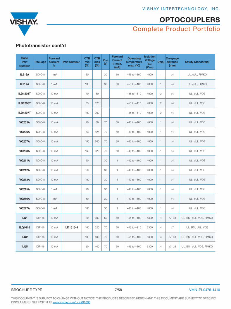
phototransistor cont’d
Base part
Numberpackage
Forward Current
IF
part NumberCTr min (%)
CTr max (%)
VCEO (V)
Forward Current IF max. (mA)
Operating Temperature
max. (°C)
Isolation Voltage
VISO (VrMS)
Ch(s)Creepage distance
(mm)Safety Standard(s)
IL216A SOIC-8 1 mA 50 30 60 –55 to +100 4000 1 ≥4 UL, cUL, FIMKO
IL217A SOIC-8 1 mA 100 30 60 –55 to +100 4000 1 ≥4 UL, cUL, FIMKO
ILD1205T SOIC-8 10 mA 40 80 –55 to +110 4000 2 ≥4 UL, cUL, VDE
ILD1206T SOIC-8 10 mA 63 125 –55 to +110 4000 2 ≥4 UL, cUL, VDE
ILD1207T SOIC-8 10 mA 100 200 –55 to +110 4000 2 ≥4 UL, cUL, VDE
VO205A SOIC-8 10 mA 40 80 70 60 –40 to +100 4000 1 ≥4 UL, cUL, VDE
VO206A SOIC-8 10 mA 63 125 70 60 –40 to +100 4000 1 ≥4 UL, cUL, VDE
VO207A SOIC-8 10 mA 100 200 70 60 –40 to +100 4000 1 ≥4 UL, cUL, VDE
VO208A SOIC-8 10 mA 160 320 70 60 –40 to +100 4000 1 ≥4 UL, cUL, VDE
VO211A SOIC-8 10 mA 20 30 1 –40 to +100 4000 1 ≥4 UL, cUL, VDE
VO212A SOIC-8 10 mA 50 30 1 –40 to +100 4000 1 ≥4 UL, cUL, VDE
VO213A SOIC-8 10 mA 100 30 1 –40 to +100 4000 1 ≥4 UL, cUL, VDE
VO215A SOIC-8 1 mA 20 30 1 –40 to +100 4000 1 ≥4 UL, cUL, VDE
VO216A SOIC-8 1 mA 50 30 1 –40 to +100 4000 1 ≥4 UL, cUL, VDE
VO217A SOIC-8 1 mA 100 30 1 –40 to +100 4000 1 ≥4 UL, cUL, VDE
ILQ1 DIP-16 10 mA 20 300 50 60 –55 to +100 5300 4 ≥7; ≥8 UL, BSI, cUL, VDE, FIMKO
ILQ1615 DIP-16 10 mA ILD1615-4 160 320 70 60 –55 to +110 5300 4 ≥7 UL, BSI, cUL, VDE
ILQ2 DIP-16 10 mA 100 500 70 60 –55 to +100 5300 4 ≥7; ≥8 UL, BSI, cUL, VDE, FIMKO
ILQ5 DIP-16 10 mA 50 400 70 60 –55 to +100 5300 4 ≥7; ≥8 UL, BSI, cUL, VDE, FIMKO
Complete Product Portfolio
THIS DOCUMENT IS SUBJECT TO CHANGE WITHOUT NOTICE. THE PRODUCTS DESCRIBED HEREIN AND THIS DOCUMENT ARE SUBJECT TO SPECIFIC DISCLAIMERS, SET FORTH AT www.vishay.com/doc?91000
VMN-PL0475-141018/58BROCHURE TyPE
OpTOCOupLErS
V I S H AY I N T E R T E C H N O LO GY, I N C .
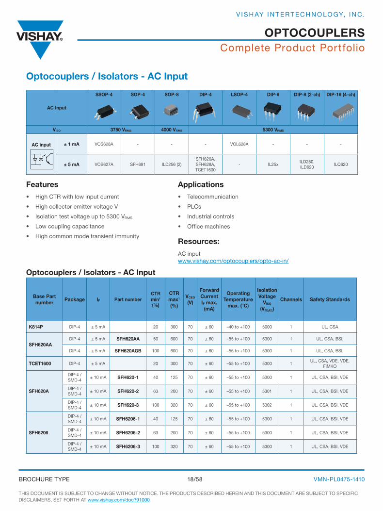
Optocouplers / Isolators - AC Input
Optocouplers / Isolators - AC Input
Base part number
package IF part numberCTr min1 (%)
CTr max1 (%)
VCEO (V)
Forward Current IF max. (mA)
Operating Temperature
max. (°C)
Isolation Voltage
VISO (VRMS)
Channels Safety Standards
K814p DIP-4 ± 5 mA 20 300 70 ± 60 –40 to +100 5000 1 UL, CSA
SFH620AADIP-4 ± 5 mA SFH620AA 50 600 70 ± 60 –55 to +100 5300 1 UL, CSA, BSI,
DIP-4 ± 5 mA SFH620AGB 100 600 70 ± 60 –55 to +100 5300 1 UL, CSA, BSI,
TCET1600 DIP-4 ± 5 mA 20 300 70 ± 60 –55 to +100 5300 1UL, CSA, VDE, VDE,
FIMKO
SFH620A
DIP-4 / SMD-4
± 10 mA SFH620-1 40 125 70 ± 60 –55 to +100 5300 1 UL, CSA, BSI, VDE
DIP-4 / SMD-4
± 10 mA SFH620-2 63 200 70 ± 60 –55 to +100 5301 1 UL, CSA, BSI, VDE
DIP-4 / SMD-4
± 10 mA SFH620-3 100 320 70 ± 60 –55 to +100 5302 1 UL, CSA, BSI, VDE
SFH6206
DIP-4 / SMD-4
± 10 mA SFH6206-1 40 125 70 ± 60 –55 to +100 5300 1 UL, CSA, BSI, VDE
DIP-4 / SMD-4
± 10 mA SFH6206-2 63 200 70 ± 60 –55 to +100 5300 1 UL, CSA, BSI, VDE
DIP-4 / SMD-4
± 10 mA SFH6206-3 100 320 70 ± 60 –55 to +100 5300 1 UL, CSA, BSI, VDE
AC Input
SSOp-4 SOp-4 SOp-8 DIp-4 LSOp-4 DIp-6 DIp-8 (2-ch) DIp-16 (4-ch)
VISO 3750 VrMS 4000 VrMS 5300 VrMS
AC input ± 1 mA VOS628A - - - VOL628A - - -
± 5 mA VOS627A SFH691 ILD256 (2)SFH620A, SFH628A, TCET1600
- IL25xILD250, ILD620
ILQ620
Applications
• Telecommunication
• PLCs
• Industrial controls
• Office machines
resources:
AC input www.vishay.com/optocouplers/opto-ac-in/
Features
• High CTR with low input current
• High collector emitter voltage V
• Isolation test voltage up to 5300 VRMS
• Low coupling capacitance
• High common mode transient immunity

Complete Product Portfolio
THIS DOCUMENT IS SUBJECT TO CHANGE WITHOUT NOTICE. THE PRODUCTS DESCRIBED HEREIN AND THIS DOCUMENT ARE SUBJECT TO SPECIFIC DISCLAIMERS, SET FORTH AT www.vishay.com/doc?91000
VMN-PL0475-141019/58BROCHURE TyPE
OpTOCOupLErS
V I S H AY I N T E R T E C H N O LO GY, I N C .
Base part number
package IF part numberCTr min1 (%)
CTr max1 (%)
VCEO (V)
Forward Current IF max. (mA)
Operating Temperature
max. (°C)
Isolation Voltage
VISO (VRMS)
Channels Safety Standards
SFH628A
DIP-4 / SMD-4
± 1 mA SFH628A-2 63 200 55 ± 50 –55 to +100 5300 1 UL, VDE, BSI
DIP-4 / SMD-4
± 1 mA SFH628A-3 100 320 55 ± 50 –55 to +100 5300 1 UL, VDE, BSI
DIP-4 / SMD-4
± 1 mA SFH628A-4 160 500 55 ± 50 –55 to +100 5300 1 UL, VDE, BSI
SFH6286
DIP-4 / SMD-4
± 1 mA SFH6286-2 63 200 55 ± 50 –55 to +100 5300 1 UL, VDE, BSI
DIP-4 / SMD-4
± 1 mA SFH6286-3 100 320 55 ± 50 –55 to +100 5300 1 UL, VDE, BSI
DIP-4 / SMD-4
± 1 mA SFH6286-4 160 500 55 ± 50 –55 to +100 5300 1 UL, VDE, BSI
SFH691A SOP-4 ± 5 mA 50 300 70 ± 50 –55 to +100 3750 1 UL, cUL, FIMKO, VDE,
TCMT1600 SOP-4 ± 5 mA 80 300 70 ± 60 –40 to +100 3750 1 UL, cUL, VDE, FIMKO, BSI
VOS627A
SSOP-4 ± 5 mA VOS627A 50 600 80 50 –55 to +110 3750 1UL, cUL, VDE, FIMKO,
CQC
SSOP-4 ± 5 mA VOS627A-2 63 125 80 50 –55 to +110 3750 1UL, cUL, VDE, FIMKO,
CQC
SSOP-4 ± 5 mA VOS627A-3 100 200 80 50 –55 to +110 3750 1UL, cUL, VDE, FIMKO,
CQC
SSOP-4 ± 5 mA VOS627A-4 160 320 80 50 –55 to +110 3750 1UL, cUL, VDE, FIMKO,
CQC
VOS628A
SSOP-4 ± 1mA VOS628A 50 600 80 50 –55 to +110 3750 1UL, cUL, VDE, FIMKO,
CQC
SSOP-4 ± 1mA VOS628A-2 63 125 80 50 –55 to +110 3750 1UL, cUL, VDE, FIMKO,
CQC
SSOP-4 ± 1mA VOS628A-3 100 200 80 50 –55 to +110 3750 1UL, cUL, VDE, FIMKO,
CQC
SSOP-4 ± 1mA VOS628A-4 160 320 80 50 –55 to +110 3750 1UL, cUL, VDE, FIMKO,
CQC
LSOP-4 ± 1mA VOL628A 50 600 80 ± 60 –55 to +110 5000 1UL, cUL, VDE, BSI, FIMKO,
CQC
LSOP-4 ± 1mA VOL628A-1 40 80 80 ± 60 –55 to +110 5000 1UL, cUL, VDE, BSI, FIMKO,
CQC
LSOP-4 ± 1mA VOL628A-2 63 125 80 ± 60 –55 to +110 5000 1UL, cUL, VDE, BSI, FIMKO,
CQC
LSOP-4 ± 1mA VOL628A-3 100 200 80 ± 60 –55 to +110 5000 1UL, cUL, VDE, BSI, FIMKO,
CQC
IL766B DIP-6 60 60 5300 1 UL, BSI
H11AA1 DIP-6 / SMD-6
± 10mA 20 30 ± 60 –55 to +100 5300 1UL, CSA, BSI, VDE,
FIMKO
IL255
DIP-6 / SMD-6
± 10 mA IL255 0.33 3 30 130 –55 to +100 5300 1 UL, cUL, BSI
DIP-6 / SMD-6
± 10 mA IL255-2 0.33 3 30 130 –55 to +100 5300 1 UL, cUL, BSI
Optocouplers / Isolators - AC Input cont’d

Complete Product Portfolio
THIS DOCUMENT IS SUBJECT TO CHANGE WITHOUT NOTICE. THE PRODUCTS DESCRIBED HEREIN AND THIS DOCUMENT ARE SUBJECT TO SPECIFIC DISCLAIMERS, SET FORTH AT www.vishay.com/doc?91000
VMN-PL0475-141020/58BROCHURE TyPE
OpTOCOupLErS
V I S H AY I N T E R T E C H N O LO GY, I N C .
Base part number
package IF part numberCTr min1 (%)
CTr max1 (%)
VCEO (V)
Forward Current IF max. (mA)
Operating Temperature
max. (°C)
Isolation Voltage
VISO (VRMS)
Channels Safety Standards
K824p DIP-8 ± 5 mA 20 300 70 ± 60 –40 to +100 5000 2 UL, CSA
TCET2600 DIP-8 ± 5 mA 20 300 70 ± 60 –55 to +100 5300 2 UL, CSA, VDE, FIMKO
ILD620
DIP-8 / SMD-8
± 5 mA ILD620 50 600 70 ± 60 –55 to +100 5300 2UL, cUL, VDE, FIMKO,
CQC
DIP-8 / SMD-8
± 5 mA ILD620GB 100 600 70 ± 60 –55 to +100 5300 2UL, cUL, VDE, FIMKO,
CQC
IL256A SOIC-8 ± 10 mA 20 30 60 –55 to +100 4000 1 UL, CSA, VDE
ILD256T SOIC-8 ± 10 mA 20 70 30 –55 to +100 4000 2 UL, VDE
TCMT4600 SOP-16 ± 5 mA 80 300 70 ± 60 –40 to +100 3750 4UL, cUL, VDE, FIMKO,
BSI
TCMT4606 SOP-16 ± 5 mA 100 300 70 ± 60 –40 to +100 3750 4UL, cUL, VDE, FIMKO,
BSI
K844p DIP-16 ± 5 mA 20 300 70 ± 60 –40 to +100 5000 4 UL, CSA
TCET4600 DIP-16 ± 5 mA 20 300 70 ± 60 –55 to +100 5300 4 UL, CSA, VDE, FIMKO
ILQ620
DIP-16 / SMD-16
± 5 mA ILQ620 50 600 70 ± 60 –55 to +100 5300 4UL, cUL, VDE, FIMKO,
CQC
DIP-16 / SMD-16
± 5 mA ILQ620GB 100 600 70 ± 60 –55 to +100 5300 4UL, cUL, VDE, FIMKO,
CQC
Optocouplers / Isolators - AC Input cont’d
Complete Product Portfolio
THIS DOCUMENT IS SUBJECT TO CHANGE WITHOUT NOTICE. THE PRODUCTS DESCRIBED HEREIN AND THIS DOCUMENT ARE SUBJECT TO SPECIFIC DISCLAIMERS, SET FORTH AT www.vishay.com/doc?91000
VMN-PL0475-141021/58BROCHURE TyPE
OpTOCOupLErS
V I S H AY I N T E R T E C H N O LO GY, I N C .
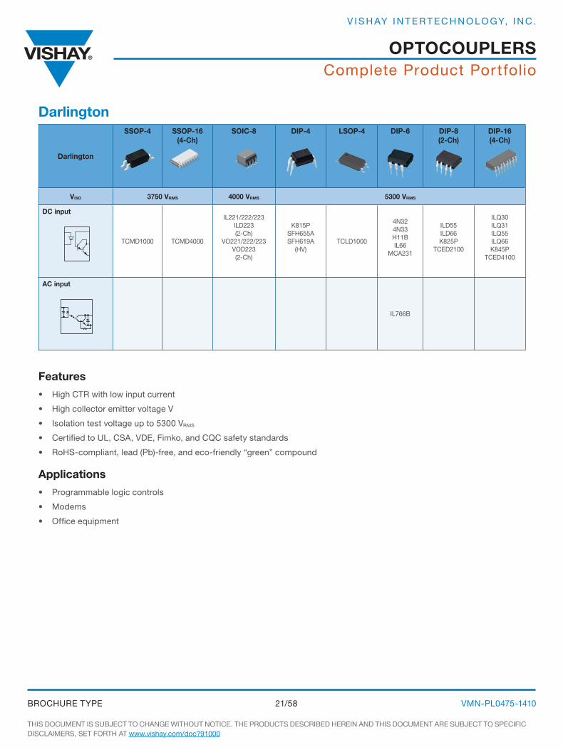
Darlington
SSOp-4 SSOp-16(4-Ch)
SOIC-8 DIp-4 LSOp-4 DIp-6 DIp-8(2-Ch)
DIp-16(4-Ch)
VISO 3750 VrMS 4000 VrMS 5300 VrMS
DC input
TCMD1000 TCMD4000
IL221/222/223ILD223(2-Ch)
VO221/222/223VOD223(2-Ch)
K815PSFH655ASFH619A
(HV)TCLD1000
4N324N33H11BIL66
MCA231
ILD55ILD66K825P
TCED2100
ILQ30ILQ31ILQ55ILQ66K845P
TCED4100
AC input
IL766B
Darlington
Features
• High CTR with low input current
• High collector emitter voltage V
• Isolation test voltage up to 5300 VRMS
• Certified to UL, CSA, VDE, Fimko, and CQC safety standards
• RoHS-compliant, lead (Pb)-free, and eco-friendly “green” compound
Applications
• Programmable logic controls
• Modems
• Office equipment
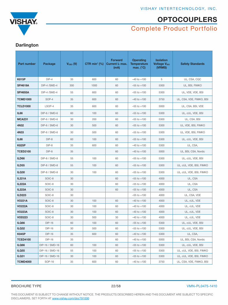
Complete Product Portfolio
THIS DOCUMENT IS SUBJECT TO CHANGE WITHOUT NOTICE. THE PRODUCTS DESCRIBED HEREIN AND THIS DOCUMENT ARE SUBJECT TO SPECIFIC DISCLAIMERS, SET FORTH AT www.vishay.com/doc?91000
VMN-PL0475-141022/58BROCHURE TyPE
OpTOCOupLErS
V I S H AY I N T E R T E C H N O LO GY, I N C .
Darlington
part number package VCEO (V) CTr min1 (%)Forward
Current IF max. (mA)
Operating Temperature
max. (°C)
Isolation Voltage VISO
(VrMS)Safety Standards
K815p DIP-4 35 600 60 –40 to +100 5 UL, CSA, CQC
SFH619A DIP-4 /SMD-4 300 1000 60 –55 to +100 5300 UL, BSI, FIMKO
SFH655A DIP-4 /SMD-4 55 600 60 –55 to +100 5300 UL, VDE, VDE, BSI
TCMD1000 SOP-4 35 600 60 –40 to +100 3750 UL, CSA, VDE, FIMKO, BSI
TCLD1000 LSOP-4 35 600 60 –55 to +100 5000 UL, CSA, BSI, VDE
IL66 DIP-6 / SMD-6 60 100 60 –55 to +100 5300 UL, cUL, VDE, BSI
MCA231 DIP-6 / SMD-6 30 200 60 –55 to +100 5300 UL, CSA, BSI
4N32 DIP-6 / SMD-6 30 500 60 –55 to +100 5300 UL, VDE, BSI, FIMKO
4N33 DIP-6 / SMD-6 30 500 60 –55 to +100 5300 UL, VDE, BSI, FIMKO
IL66 DIP-8 60 100 60 –55 to +100 5300 UL, cUL, VDE, BSI
K825p DIP-8 35 600 60 –40 to +100 5300 UL, CSA,
TCED2100 DIP-8 35 60 –40 to +100 5000 UL, BSI, CSA, Nordic
ILD66 DIP-8 / SMD-8 55 100 60 –55 to +100 5300 UL, cUL, VDE, BSI
ILD55 DIP-8 / SMD-8 55 100 60 –55 to +100 5300 UL, cUL, VDE, BSI, FIMKO
ILQ30 DIP-8 / SMD-8 30 100 60 –55 to +100 5300 UL, cUL, VDE, BSI, FIMKO
IL221A SOIC-8 30 60 –55 to +100 4000 UL, CSA
IL222A SOIC-8 30 60 –55 to +100 4000 UL, CSA
IL223A SOIC-8 30 60 –55 to +100 4000 UL, CSA
ILD223 SOIC-8 30 –55 to +100 4000 UL, CSA, VDE
VO221A SOIC-8 30 100 60 –40 to +100 4000 UL, cUL, VDE
VO222A SOIC-8 30 100 60 –40 to +100 4000 UL, cUL, VDE
VO223A SOIC-8 30 100 60 –40 to +100 4000 UL, cUL, VDE
VOD223 SOIC-8 30 500 30 –40 to +100 4000 UL, cUL, VDE
ILQ66 DIP-16 60 100 60 –55 to +100 5300 UL, cUL, VDE, BSI
ILQ32 DIP-16 30 500 60 –55 to +100 5300 UL, cUL, VDE, BSI
K845p DIP-16 35 600 60 –40 to +100 5300 UL, CSA,
TCED4100 DIP-16 35 60 –40 to +100 5000 UL, BSI, CSA, Nordic
ILQ66 DIP-16 / SMD-16 60 100 60 –55 to +100 5300 UL, cUL, VDE, BSI
ILQ55 DIP-16 / SMD-16 55 100 60 –55 to +100 5300 UL, cUL, VDE, BSI, FIMKO
ILQ31 DIP-16 / SMD-16 30 100 60 –55 to +100 5300 UL, cUL, VDE, BSI, FIMKO
TCMD4000 SOP-16 35 600 60 –40 to +100 3750 UL, CSA, VDE, FIMKO, BSI
Complete Product Portfolio
THIS DOCUMENT IS SUBJECT TO CHANGE WITHOUT NOTICE. THE PRODUCTS DESCRIBED HEREIN AND THIS DOCUMENT ARE SUBJECT TO SPECIFIC DISCLAIMERS, SET FORTH AT www.vishay.com/doc?91000
VMN-PL0475-141023/58BROCHURE TyPE
OpTOCOupLErS
V I S H AY I N T E R T E C H N O LO GY, I N C .
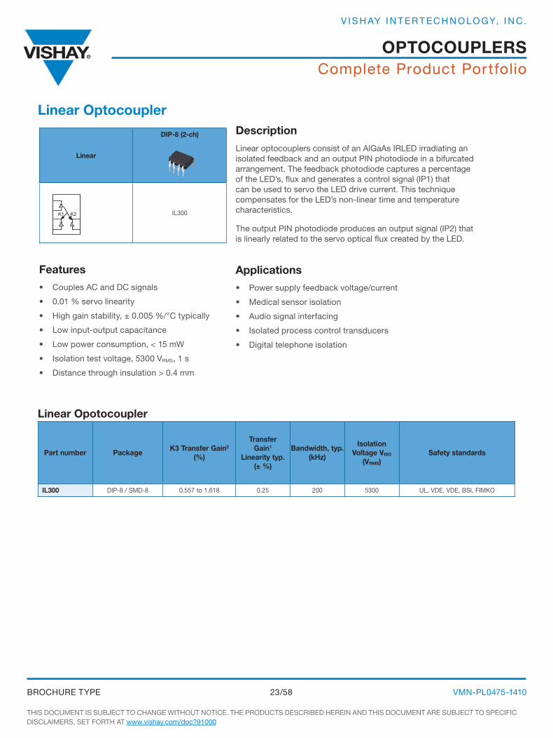
Linear Optocoupler
Features
• Couples AC and DC signals
• 0.01 % servo linearity
• High gain stability, ± 0.005 %/°C typically
• Low input-output capacitance
• Low power consumption, < 15 mW
• Isolation test voltage, 5300 VRMS, 1 s
• Distance through insulation > 0.4 mm
Linear Opotocoupler
part number packageK3 Transfer Gain2
(%)
Transfer Gain1
Linearity typ. (± %)
Bandwidth, typ. (kHz)
Isolation Voltage VISO
(VrMS)Safety standards
IL300 DIP-8 / SMD-8 0.557 to 1.618 0.25 200 5300 UL, VDE, VDE, BSI, FIMKO
Linear
DIp-8 (2-ch)
IL300K2K1
Applications
• Power supply feedback voltage/current
• Medical sensor isolation
• Audio signal interfacing
• Isolated process control transducers
• Digital telephone isolation
Description
Linear optocouplers consist of an AlGaAs IRLED irradiating an isolated feedback and an output PIN photodiode in a bifurcated arrangement. The feedback photodiode captures a percentage of the LED’s, flux and generates a control signal (IP1) that can be used to servo the LED drive current. This technique compensates for the LED’s non-linear time and temperature characteristics.
The output PIN photodiode produces an output signal (IP2) that is linearly related to the servo optical flux created by the LED.

Complete Product Portfolio
THIS DOCUMENT IS SUBJECT TO CHANGE WITHOUT NOTICE. THE PRODUCTS DESCRIBED HEREIN AND THIS DOCUMENT ARE SUBJECT TO SPECIFIC DISCLAIMERS, SET FORTH AT www.vishay.com/doc?91000
VMN-PL0475-141024/58BROCHURE TyPE
OpTOCOupLErS
V I S H AY I N T E R T E C H N O LO GY, I N C .
High-Speed Optocouplers
Features
• JEDEC-compatible
• Reinforced insulation
• High-voltage isolation
• Up to 30 kV/μs common mode transient immunity
• Isolation test voltages up to 5300 VRMS
Applications
• Industrial communication buses
• High-speed A/D and D/A converters
• Digital control and switch mode power supplies
• Industrial controller I/O interfaces
• Scan driver IC interfaces for high output voltage devices (plasma display panels)
• Signal isolation transformer replacement
• AC motor drives
• IPM drivers
High-Speed Optocouplers (Analog)
part number
packageData rate
(MBd)
CTrmin (%)
tpLH typ. (µs)
tpHL typ. (µs)
CMTI typ (V/µsec)
Operating Temperature
(°C)
Isolation Voltage
VISO (VrMS)
Ch(s)Creepage distance
(mm)
Safety Standard(s)
6N1135 DIP-8; DIP-8, 400 mil; SMD-8
1 7 0.2 0.2 1000 -55 to + 110 5300 1 >7, >8 UL, VDE, cUL
6N1136 DIP-8; DIP-8, 400 mil; SMD-8
1 19 0.2 0.2 1000 -55 to + 110 5300 1 >7, >8 UL, VDE, cUL
6N135 DIP-8; SMD-8 1 7 0.2 0.2 1000 -55 to + 100 5300 1 >7 UL, VDE, cUL
6N136 DIP-8; DIP-8, 400 mil; SMD-8
1 19 0.2 0.2 1000 -55 to + 100 5300 1 >7, >8 UL, VDE, cUL
6N138 DIP-8; SMD-8 0.1 300 1 0.6 500 -55 to + 100 5300 1 >7 UL, VDE, cUL
6N139 DIP-8; SMD-8 0.1 500 1 0.6 500 -55 to + 100 5300 1 >7 UL, VDE, cUL
SFH6135 DIP-8; DIP-8, 400 mil; SMD-8
1 7 0.2 0.2 1000 -55 to + 100 5300 1 >7, >8 UL, VDE, cUL
SFH6136 DIP-8; DIP-8, 400 mil; SMD-8
1 19 0.2 0.2 1000 -55 to + 100 5300 1 >7, >8 UL, VDE, cUL
SFH6138 DIP-8 0.1 300 1 0.6 500 -55 to + 100 5300 1 >7 UL, VDE
SFH6139 DIP-8; DIP-8, 400 mil; SMD-8
0.1 500 1 0.6 500 -55 to + 100 5300 1 >7, >8 UL, VDE
SFH6315 SOIC-8 1 7 0.5 0.25 1000 -55 to + 100 4000 1 >4 UL, VDE, cUL
resources
• Analog www.vishay.com/optocouplers/opto-high-analog/
• Digital www.vishay.com/optocouplers/opto-high-digital/
>>>

Complete Product Portfolio
THIS DOCUMENT IS SUBJECT TO CHANGE WITHOUT NOTICE. THE PRODUCTS DESCRIBED HEREIN AND THIS DOCUMENT ARE SUBJECT TO SPECIFIC DISCLAIMERS, SET FORTH AT www.vishay.com/doc?91000
VMN-PL0475-141025/58BROCHURE TyPE
OpTOCOupLErS
V I S H AY I N T E R T E C H N O LO GY, I N C .
part number
packageData rate
(MBd)
CTrmin (%)
tpLH typ. (µs)
tpHL typ. (µs)
CMTI typ (V/µsec)
Operating Temperature
(°C)
Isolation Voltage
VISO (VrMS)
Ch(s)Creepage distance
(mm)
Safety Standard(s)
SFH6316 SOIC-8 1 19 0.5 0.25 1000 -55 to + 100 4000 1 >4 UL, VDE, cUL
SFH6318 SOIC-8 0.1 300 2 2 1000 -55 to + 100 4000 1 >4 UL, VDE, cUL
SFH6319 SOIC-8 0.1 500 0.6 1.5 1000 -55 to + 100 4000 1 >4 UL, VDE, cUL
SFH6319 SOIC-8 0.1 500 0.6 1.5 1000 -55 to + 100 4000 1 >4 UL, VDE, cUL
SFH6325 DIP-8; SMD-8 1 7 0.5 0.25 150001 -55 to + 100 5300 2 >7 UL, VDE, cUL
SFH6326 DIP-8; DIP-8, 400 mil; SMD-8
1 19 0.5 0.25 150001 -55 to + 100 5300 2 >7, >8 UL, VDE, cUL
SFH6343 SOIC-8 1 19 0.5 0.25 150001 -55 to + 100 4000 1 >4 UL, VDE, cUL
SFH6345 DIP-8; DIP-8, 400 mil; SMD-8
1 19 0.3 0.3 150001 -55 to + 100 5300 1 >7, >8 UL, VDE
SFH636 DIP-6; DIP-6, 400 mil; SMD-6
1 19 0.3 0.3 100001 -55 to + 100 5300 1 >7, >8
VOM452 SOP-4, 100 mil 1 15 0.2 0.5 10001 -55 to + 100 3750 1 >5 UL, VDE
VOM453 SOP-4, 100 mil 1 15 0.2 0.5 150001 -55 to + 100 3750 1 >5 UL, VDE
VOW135 DIP-8, 400mil Wide Body
1 7 1.3 0.2 10001 -40 to + 100 5300 1 >10UL, VDE, cUL,
CQC
VOW136 DIP-8, 400mil Wide Body
1 19 6 0.2 10001 -40 to + 100 5300 1 >10UL, VDE, cUL,
CQC
Note: 1
= minimum value
High-Speed Optocouplers (Analog) cont’d

Complete Product Portfolio
THIS DOCUMENT IS SUBJECT TO CHANGE WITHOUT NOTICE. THE PRODUCTS DESCRIBED HEREIN AND THIS DOCUMENT ARE SUBJECT TO SPECIFIC DISCLAIMERS, SET FORTH AT www.vishay.com/doc?91000
VMN-PL0475-141026/58BROCHURE TyPE
OpTOCOupLErS
V I S H AY I N T E R T E C H N O LO GY, I N C .
High-Speed Optocouplers (Digital)
part number packageData rate
(MBd)
tpLH typ. (ns)
tpHL typ. (ns)
pulse Width Distortion pWD (ns)
CMTI typ
(V/µsec)
CMTI min
(V/µsec)
Operating Temperature
(°C)
Isolation Voltage VISO
(VrMS)Ch(s)
Creepage Distance
(mm)\
Safety Standards
6N137 DIP-8; DIP-8, 400mil, SMD-8
10 48 50 2.9 25000 -40 to + 100 5300 1 >7, >8UL, VDE,
cUL
6N137A DIP-8; SMD-8 10 45 32 2.9 25000 -40 to + 100 1 >7UL, VDE,
cUL
SFH6700 DIP-8; SMD-8 5 120 125 1000 -40 to + 85 5300 1 >7 UL, VDE
SFH6701 DIP-8; SMD-8 5 120 125 1000 -40 to + 85 5300 1 >7 UL, VDE
SFH6702 DIP-8; DIP-8, 400mil, SMD-8
5 120 125 1000 -40 to + 85 5300 1 >7, >8 UL, VDE
SFH6705 DIP-8; DIP-8, 400mil, SMD-8
5 120 125 1000 -40 to + 85 5300 1 >7, >8 UL, VDE
SFH6711 DIP-8; SMD-8 5 120 125 2500 -40 to + 85 5300 1 >7 UL, VDE
SFH6712 DIP-8; SMD-8 5 120 125 2500 -40 to + 85 5300 1 >7 UL, VDE
SFH6719 DIP-8 5 120 125 2500 -40 to + 85 5300 1 >7 UL, VDE
SFH6720 SOIC-8 5 120 125 1000 -40 to + 85 4000 1 >4 UL, VDE
SFH6721 SOIC-8 5 120 125 2500 -40 to + 85 4000 1 >4 UL, VDE
SFH6731 DIP-8; SMD-8 5 120 125 1000 -40 to + 85 5300 2 >7 UL, VDE
SFH6732 DIP-8; SMD-8 5 120 125 5000 -40 to + 85 5300 2 >7 UL, VDE
SFH6755 SOIC-8 10 48 50 2.9 10000 -40 to + 100 4000 2
SFH6756 SOIC-8 10 48 50 2.9 5000 -40 to + 100 4000 2
SFH6757 SOIC-8 10 48 50 2.9 10000 -40 to + 100 4000 2
VO0600 SOIC-8 10 48 50 2.9 1000 -40 to + 100 4000 1UL, VDE,
cUL
VO0601 SOIC-8 10 48 50 2.9 5000 -40 to + 100 4000 1UL, VDE,
cUL
VO0611 SOIC-8 10 48 50 2.9 10000 -40 to + 100 4000 1UL, VDE,
cUL
vo0630 SOIC-8 10 48 50 2.9 1000 -40 to + 100 4000 2 >4UL, VDE,
cUL
vo0631 SOIC-8 10 48 50 2.9 5000 -40 to + 100 4000 2 >4UL, VDE,
cUL
vo0661 SOIC-8 10 48 50 2.9 10000 -40 to + 100 4000 2 >4UL, VDE,
cUL
VO2601 DIP-8; DIP-8, 400mil, SMD-8
10 48 50 2.9 5000 -40 to + 100 5300 1 >7, >8UL, VDE,
cUL
VO2611 DIP-8; DIP-8, 400mil, SMD-8
10 48 50 2.9 10000 -40 to + 100 5300 1 >7, >8UL, VDE,
cUL
VO2630 DIP-8; DIP-8, 400mil, SMD-8
10 48 50 2.9 1000 -40 to + 100 5300 2 >7, >8UL, VDE,
cUL
VO2631 DIP-8; DIP-8, 400mil, SMD-8
10 48 50 2.9 5000 -40 to + 100 5300 2 >7, >8UL, VDE,
cUL
VO4661 DIP-8; DIP-8, 400mil, SMD-8
10 48 50 2.9 10000 -40 to + 100 5300 2 >7, >8UL, VDE,
cUL
VOW137 DIP-8, 400mil Wide Body
10 49 46 3.1 10000 -40 to + 100 5300 1 >10UL, VDE, cUL, CQC
VOW2611 DIP-8, 400mil Wide Body
10 49 46 3.1 20000 -40 to + 100 5300 1 >10UL, VDE, cUL, CQC

Complete Product Portfolio
THIS DOCUMENT IS SUBJECT TO CHANGE WITHOUT NOTICE. THE PRODUCTS DESCRIBED HEREIN AND THIS DOCUMENT ARE SUBJECT TO SPECIFIC DISCLAIMERS, SET FORTH AT www.vishay.com/doc?91000
VMN-PL0475-141027/58BROCHURE TyPE
OpTOCOupLErS
V I S H AY I N T E R T E C H N O LO GY, I N C .
phototriac
DIp-6 / SMD-6 SOp-4 DIp-16 DIp-8 (6)
Min/ Dv/dt 10 000 V/µs 5000 V/µs ≤ 1500 V/µs ≤ 1500 V/µs 500 V/µs 10 V/µs
Zero Crossing
400 V BRT21 VO4154 - - - -
600 VIL410IL4116
IL4117 (700 V)
VO4156VO3062VO3063VO4157(700 V)
VO3062VO3063
-VO2223
VO2223A-
800 VIL4108IL4118
VO4158 - - - -
Non-Zero Crossing 250 V - -
K3010K3011K3012K3013
- - -
400 V BRT11 VO4254
VO3020VO3021VO3022VO3023K3020K3022K3023
- - -
600 VIL420
IL4216IL4217 (700 V)
VO4256VO4257 (700 V)
VO3252VO3253
VOM3052VOM3053VOM160
VO3526 -
800 VIL4208IL4218
VO4258 - - - -
*Zero crossing circuit
ZCC*
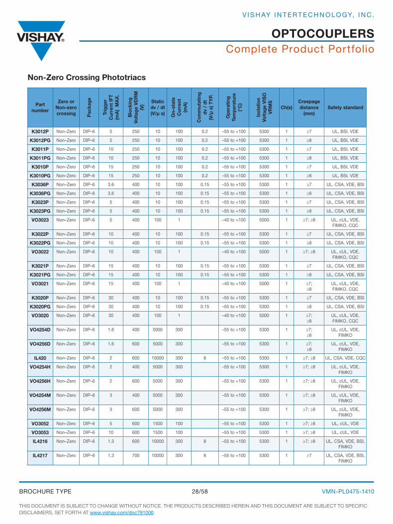
phototriacs
Features
• Zero crossing or non-zero crossing
• dV/dt range: 10 kV/μs, 5 kV/μs, 1.5 kV/μs, 0.5 kV/μs, 10 V/μs
• VDRM range: 250 V, 400 V, 600 V, 700 V, 800 V Isolation test voltage up to 5300 VRMS
• Worldwide safety agency certifications: UL, cUL, CSA, CQC, VDE, DIN EN (60747-5-5), FIMKO
• DIP, SMD, SOP with leadbend options available
Applications
• AC Solid-state relays
• Lighting controls
• AC motor starters and drives
• Utilities metering over AC lines
• Solenoid/valve controls
• Temperature controls
• Electromechanical contactors
resources
• www.vishay.com/optocouplers/opto-triac/
Complete Product Portfolio
THIS DOCUMENT IS SUBJECT TO CHANGE WITHOUT NOTICE. THE PRODUCTS DESCRIBED HEREIN AND THIS DOCUMENT ARE SUBJECT TO SPECIFIC DISCLAIMERS, SET FORTH AT www.vishay.com/doc?91000
VMN-PL0475-141028/58BROCHURE TyPE
OpTOCOupLErS
V I S H AY I N T E R T E C H N O LO GY, I N C .
Non-Zero Crossing phototriacs
part number
Zero or Non–zero crossing p
acka
ge
Trig
ger
Cur
rent
IFT
(mA
) M
AX
.
Blo
ckin
g Vo
ltage
VD
rM
(V
) Static dv / dt (V/μ s) O
n–st
ate
Cur
rent
(m
A)
Com
mut
atin
g dv
/ d
t
(V/μ
s) T
Yp.
Ope
ratin
g Te
mpe
ratu
re
(°C
)
Isol
atio
n Vo
ltage
VIS
O
Vr
MS
Ch(s)Creepage distance
(mm)Safety standard
K3012p Non–Zero DIP–6 5 250 10 100 0.2 –55 to +100 5300 1 ≥7 UL, BSI, VDE
K3012pG Non–Zero DIP–6 5 250 10 100 0.2 –55 to +100 5300 1 ≥8 UL, BSI, VDE
K3011p Non–Zero DIP–6 10 250 10 100 0.2 –55 to +100 5300 1 ≥7 UL, BSI, VDE
K3011pG Non–Zero DIP–6 10 250 10 100 0.2 –55 to +100 5300 1 ≥8 UL, BSI, VDE
K3010p Non–Zero DIP–6 15 250 10 100 0.2 –55 to +100 5300 1 ≥7 UL, BSI, VDE
K3010pG Non–Zero DIP–6 15 250 10 100 0.2 –55 to +100 5300 1 ≥8 UL, BSI, VDE
K3036p Non–Zero DIP–6 3.6 400 10 100 0.15 –55 to +100 5300 1 ≥7 UL, CSA, VDE, BSI
K3036pG Non–Zero DIP–6 3.6 400 10 100 0.15 –55 to +100 5300 1 ≥8 UL, CSA, VDE, BSI
K3023p Non–Zero DIP–6 5 400 10 100 0.15 –55 to +100 5300 1 ≥7 UL, CSA, VDE, BSI
K3023pG Non–Zero DIP–6 5 400 10 100 0.15 –55 to +100 5300 1 ≥8 UL, CSA, VDE, BSI
VO3023 Non–Zero DIP–6 5 400 100 1 –40 to +100 5000 1 ≥7; ≥8 UL, cUL, VDE, FIMKO, CQC
K3022p Non–Zero DIP–6 10 400 10 100 0.15 –55 to +100 5300 1 ≥7 UL, CSA, VDE, BSI
K3022pG Non–Zero DIP–6 10 400 10 100 0.15 –55 to +100 5300 1 ≥8 UL, CSA, VDE, BSI
VO3022 Non–Zero DIP–6 10 400 100 1 –40 to +100 5000 1 ≥7; ≥8 UL, cUL, VDE, FIMKO, CQC
K3021p Non–Zero DIP–6 15 400 10 100 0.15 –55 to +100 5300 1 ≥7 UL, CSA, VDE, BSI
K3021pG Non–Zero DIP–6 15 400 10 100 0.15 –55 to +100 5300 1 ≥8 UL, CSA, VDE, BSI
VO3021 Non–Zero DIP–6 15 400 100 1 –40 to +100 5000 1 ≥7; ≥8
UL, cUL, VDE, FIMKO, CQC
K3020p Non–Zero DIP–6 30 400 10 100 0.15 –55 to +100 5300 1 ≥7 UL, CSA, VDE, BSI
K3020pG Non–Zero DIP–6 30 400 10 100 0.15 –55 to +100 5300 1 ≥8 UL, CSA, VDE, BSI
VO3020 Non–Zero DIP–6 30 400 100 1 –40 to +100 5000 1 ≥7; ≥8
UL, cUL, VDE, FIMKO, CQC
VO4254D Non–Zero DIP–6 1.6 400 5000 300 –55 to +100 5300 1 ≥7; ≥8
UL, cUL, VDE, FIMKO
VO4256D Non–Zero DIP–6 1.6 600 5000 300 –55 to +100 5300 1 ≥7; ≥8
UL, cUL, VDE, FIMKO
IL420 Non–Zero DIP–6 2 600 10000 300 8 –55 to +100 5300 1 ≥7; ≥8 UL, CSA, VDE, CQC
VO4254H Non–Zero DIP–6 2 400 5000 300 –55 to +100 5300 1 ≥7; ≥8 UL, cUL, VDE, FIMKO
VO4256H Non–Zero DIP–6 2 600 5000 300 –55 to +100 5300 1 ≥7; ≥8 UL, cUL, VDE, FIMKO
VO4254M Non–Zero DIP–6 3 400 5000 300 –55 to +100 5300 1 ≥7; ≥8 UL, cUL, VDE, FIMKO
VO4256M Non–Zero DIP–6 3 600 5000 300 –55 to +100 5300 1 ≥7; ≥8 UL, cUL, VDE, FIMKO
VO3052 Non–Zero DIP–6 5 600 1500 100 –55 to +100 5300 1 ≥7; ≥8 UL, cUL, VDE
VO3053 Non–Zero DIP–6 10 600 1500 100 –55 to +100 5300 1 ≥7; ≥8 UL, cUL, VDE
IL4216 Non–Zero DIP–6 1.3 600 10000 300 8 –55 to +100 5300 1 ≥7; ≥8 UL, CSA, VDE, BSI, FIMKO
IL4217 Non–Zero DIP–6 1.3 700 10000 300 8 –55 to +100 5300 1 ≥7 UL, CSA, VDE, BSI, FIMKO

Complete Product Portfolio
THIS DOCUMENT IS SUBJECT TO CHANGE WITHOUT NOTICE. THE PRODUCTS DESCRIBED HEREIN AND THIS DOCUMENT ARE SUBJECT TO SPECIFIC DISCLAIMERS, SET FORTH AT www.vishay.com/doc?91000
VMN-PL0475-141029/58BROCHURE TyPE
OpTOCOupLErS
V I S H AY I N T E R T E C H N O LO GY, I N C .
Non-Zero Crossing phototriacs cont’d
part number
Zero or Non–zero crossing p
acka
ge
Trig
ger
Cur
rent
IFT
(mA
) M
AX
.
Blo
ckin
g Vo
ltage
VD
rM
(V
) Static dv / dt (V/μ s) O
n–st
ate
Cur
rent
(m
A)
Com
mut
atin
g dv
/ d
t
(V/μ
s) T
Yp.
Ope
ratin
g Te
mpe
ratu
re
(°C
)
Isol
atio
n Vo
ltage
VIS
O
Vr
MS
Ch(s)Creepage distance
(mm)Safety standard
VO4257D Non–Zero DIP–6 1.6 700 5000 300 –55 to +100 5300 1 ≥7; ≥8 UL, cUL, VDE
VO4258D Non–Zero DIP–6 1.6 800 5000 300 –55 to +100 5300 1 ≥7; ≥8 UL, cUL, VDE
IL4208 Non–Zero DIP–6 2 800 10000 300 8 –55 to +100 5300 1 ≥7 UL, CSA, VDE, CQC
VO4257H Non–Zero DIP–6 2 700 5000 300 –55 to +100 5300 1 ≥7; ≥8 UL, cUL, VDE
VO4258H Non–Zero DIP–6 2 800 5000 300 –55 to +100 5300 1 ≥7; ≥8 UL, cUL, VDE
VO4257M Non–Zero DIP–6 3 700 5000 300 –55 to +100 5300 1 ≥7; ≥8 UL, cUL, VDE
VO4258M Non–Zero DIP–6 3 800 5000 300 –55 to +100 5300 1 ≥7; ≥8 UL, cUL, VDE
IL4218 Non–Zero DIP–6 1.3 800 10000 300 8 –55 to +100 5300 1 ≥7; ≥8 UL, CSA, VDE, BSI, FIMKO
VOM160N Non–Zero SOP–4 5 600 500 70 0.13 –40 to +100 3750 1 ≥5 UL, cUL, CQC
VOM160p Non–Zero SOP–4 7 600 500 70 0.13 –40 to +100 3750 1 ≥5 UL, cUL, CQC
VOM160r Non–Zero SOP–4 10 600 500 70 0.13 –40 to +100 3750 1 ≥5 UL, cUL, CQC
VOM3052 Non–Zero SOP–4 5 600 1500 70 0.13 –40 to +100 3750 1 ≥5 UL, cUL, CQC
VOM3053 Non–Zero SOP–4 10 600 1500 70 0.13 –40 to +100 3750 1 ≥5 UL, cUL, CQC
VO2223 Non–Zero DIP–6 10 600 1 0.7 –40 to +85 5300 1 ≥7 UL, cUL
VO2223A Non–Zero DIP–6 10 600 1 0.7 –40 to +85 5300 1 ≥7 UL, cUL
VO3526 Non–Zero DIP–10 10 600 1 0.9 –40 to +85 5300 1 ≥7 UL, cUL

Complete Product Portfolio
THIS DOCUMENT IS SUBJECT TO CHANGE WITHOUT NOTICE. THE PRODUCTS DESCRIBED HEREIN AND THIS DOCUMENT ARE SUBJECT TO SPECIFIC DISCLAIMERS, SET FORTH AT www.vishay.com/doc?91000
VMN-PL0475-141030/58BROCHURE TyPE
OpTOCOupLErS
V I S H AY I N T E R T E C H N O LO GY, I N C .
Zero Crossing phototriacs
part number
Zero or Non–zero crossing
package
Trig
ger
Cur
rent
IFT
(mA
) M
AX
.
Blo
ckin
g Vo
ltage
VD
rM
(V
)
Sta
tic d
v /
dt
(V/μ
s)
On–
stat
e C
urre
nt (m
A)
Com
mut
atin
g dv
/ d
t
(V/μ
s) T
Yp.
Ope
ratin
g Te
mpe
ratu
re
(°C
)
Isol
atio
n Vo
ltage
VIS
O
Vr
MS
Ch(s)Creepage distance
(mm)
Safety standard
VO3062 Zero DIP–6 5 600 1500 100 –55 to +100 5300 1 ≥7; ≥8 UL, cUL, VDE
VO3063 Zero DIP–6 10 600 1500 100 –55 to +100 5300 1 ≥7; ≥8 UL, cUL, VDE
VO4154D Zero DIP–6 1.6 400 5000 300 –55 to +100 5300 1 ≥7; ≥8 UL, cUL, VDE
VO4156D Zero DIP–6 1.6 600 5000 300 –55 to +100 5300 1 ≥7; ≥8 UL, cUL, VDE
VO4154H Zero DIP–6 2 400 5000 300 –55 to +100 5300 1 ≥7; ≥8 UL, cUL, VDE
VO4156H Zero DIP–6 2 600 5000 300 –55 to +100 5300 1 ≥7; ≥8 UL, cUL, VDE
VO4154M Zero DIP–6 3 400 5000 300 –55 to +100 5300 1 ≥7; ≥8 UL, cUL, VDE
VO4156M Zero DIP–6 3 600 5000 300 –55 to +100 5300 1 ≥7; ≥8 UL, cUL, VDE
IL4116 Zero DIP–6 1.3 600 10000 300 8 –55 to +100 5300 1 ≥7; ≥8 UL, CSA, BSI, VDE, FIMKO
IL410 Zero DIP–6 2 to +6 600 10000 300 8 –55 to +100 5300 1 ≥7; ≥8 UL, CSA, VDE
IL4117 Zero DIP–6 1.3 700 10000 300 8 –55 to +100 5300 1 ≥7; ≥8 UL, CSA, BSI, VDE, FIMKO
VO4157D Zero DIP–6 1.6 800 5000 300 –55 to +100 5300 1 ≥7; ≥8 UL, cUL, VDE, FIMKO
VO4158D Zero DIP–6 1.6 800 5000 300 –55 to +100 5300 1 ≥7; ≥8 UL, cUL, VDE, FIMKO
VO4157H Zero DIP–6 2 800 5000 300 –55 to +100 5300 1 ≥7; ≥8 UL, cUL, VDE, FIMKO
VO4158H Zero DIP–6 2 800 5000 300 –55 to +100 5300 1 ≥7; ≥8 UL, cUL, VDE, FIMKO
VO4157M Zero DIP–6 3 800 5000 300 –55 to +100 5300 1 ≥7; ≥8 UL, cUL, VDE, FIMKO
VO4158M Zero DIP–6 3 800 5000 300 –55 to +100 5300 1 ≥7; ≥8 UL, cUL, VDE, FIMKO
IL4118 Zero DIP–6 1.3 800 10000 300 8 –55 to +100 5300 1 ≥7 UL, CSA, BSI, VDE, FIMKO
IL4108 Zero DIP–6 2 to +6 800 10000 300 8 –55 to +100 5300 1 ≥7; ≥8 UL, CSA, VDE

Complete Product Portfolio
THIS DOCUMENT IS SUBJECT TO CHANGE WITHOUT NOTICE. THE PRODUCTS DESCRIBED HEREIN AND THIS DOCUMENT ARE SUBJECT TO SPECIFIC DISCLAIMERS, SET FORTH AT www.vishay.com/doc?91000
VMN-PL0475-141031/58BROCHURE TyPE
OpTOCOupLErS
V I S H AY I N T E R T E C H N O LO GY, I N C .
Introduction
Vishay’s solid-state relays (SSRs) deliver fast switching while optically isolating and protecting equipment from damaging external high-voltage spikes. By eliminating the majority of wire bonds found in other SSRs, Vishay’s monolithic structure has set the performance standard.With no moving parts, our SSRs relays are noiseless, bounce-free, and reliable, commonly replacing electromechanical relays. Used in industrial, automotive, and communication applications, all of our SSRs feature low power consumption, small packaging, and low turn-on current. Exceeding industry standards, they are approved by VDE, UL, CSA and other safety regulatory agencies.
Features
• Reliable, long life, no noise, contact bounce or arcing
• Low power consumption at 75 % lower than EMR
• Low capacitance SSRs (3.5 pF)
• High-frequency SSRs (< 50 mhz)
Applications
• Telecom switches
• ATE test equipment
• Alarm control systems
resources
• Datasheets: www.vishay.com/solid-state-relays/
• SSR application notes: www.vishay.com/solid-state-relays/related/#appnot
Solid-State relays
Solid State relays (SSrs)
SSOp-8 SOp-8 SOp-4 DIp-6 DIp-8 (1-Ch)
DIp-8(2-Ch)
Types
VISO
2500 VrMS 3000 VrMS 3750 VrMS 5300 VrMSOff state voltage
1 Form A
60 V - - VO1400AEFTR VO14642A - -
200 V - - - LH1510A -LH1522ALH1544A
250 V - - - LH1518A - LH1505A
350 V LH1540ACDLH1532 LH1529 LH1546AEF
LH1500ALH1546ALH1550A
LH1529A(with Optocoupler)
LH1520ALH1532ALH1533ALH1556A
400 V - - - LH1525A - LH1526A
200 V - - - LH1511B - LH1523B
350 V - - - LH1501B - LH1521B
1 Form A/B, C 200 V - - - - LH1512B -
350 V - - - - LH1502B -
2 Form A 200 V - - - - LH1513A -
350 V - - - - LH1503A -
MOSFET Driver - - VOM1271 - LH1262C VO1263A -

Complete Product Portfolio
THIS DOCUMENT IS SUBJECT TO CHANGE WITHOUT NOTICE. THE PRODUCTS DESCRIBED HEREIN AND THIS DOCUMENT ARE SUBJECT TO SPECIFIC DISCLAIMERS, SET FORTH AT www.vishay.com/doc?91000
VMN-PL0475-141032/58BROCHURE TyPE
OpTOCOupLErS
V I S H AY I N T E R T E C H N O LO GY, I N C .
Solid-State relays
part number Type p
acka
ge
Load
Vol
tage
Max
(V
)
Load
Cur
rent
Max
. r
ecom
men
ded
(mA
) - A
C/D
C
Load
Cur
rent
Max
. r
ecom
men
ded
(mA
) -D
C
On-
res
ista
nce
Max
. at
25 °
C (Ω
) -A
C/D
C
On-
res
ista
nce
Max
. at
25 °
C (Ω
) -D
C
Cur
rent
Lim
it (m
A),
Typ.
at
25 °
C, I
F =
5 m
A -
AC
/DC
ton toff
Isol
atio
n Vo
ltage
V
ISO
Vr
MS
CH(s)
LH1546AEF
1 Form A
SOP-4 350 120 — 35 — — 3 3 5300 1
VO1400AEFTr DIP-4 60 100 — 5 — — 0.5 0.5 5300 1
LH15109 DIP-6 200 200 350 15 3.75 360 2.0* 2.0* 5300 1
LH1518 DIP-6 250 155 300 20 5 28010 3 3 5300 1
LH1500 DIP-6 350 150 250 25 6.25 270 2 2 5300 1
LH1540 DIP-6 350 120 250 25 6.25 210 2 2 5300 1
LH1546A DIP-6 350 120 35 200 3 3 5300 1
LH15501 DIP-6 350 100 — 50 — 200 3 3 5300 1
VO14642 DIP-6 60 1000 2000 0.25 0.07 — 0.8* 0.8* 5300 1
LH15132 Form A
DIP-8 200 140 — 15 — 360 2.5* 2.5* 5300 1
LH1503 DIP-8 350 110 — 25 — 270 2.5* 2.5* 5300 1
LH1522
1 Form A
DIP-8 200 140 — 15 — 360 2.0* 2.0* 5300 2
LH15441 DIP-8 200 40 — 160 — — 0.5 0.5 5300 2
LH1505 DIP-8 250 120 — 20 — 200 4 4 5300 2
LH1520 DIP-8 350 110 — 25 — 270 2 2 5300 2
LH1526 DIP-8 400 100 — 36 — 210 1 1.5 5300 2
LH15325 DIP-8 350 110 — 25 — 210 2 2.5 5300 2
LH1533 DIP-8 350 70 — 50 — 200 3 3 5300 2
LH15565 DIP-8 350 120 — 35 — 210 3 3 5300 2
LH1511
1 Form B
DIP-6 200 200 300 15 3.75 — 3.0* 3.0* 5300 1
LH1501 DIP-6 350 150 200 25 6.25 — 3 3 5300 1
LH1521 DIP-8 350 110 — 25 — — 3 3 5300 2
LH15231 Form A
DIP-8 200 140 — 15 — — 3.0* 3.0* 5300 2
LH15022 DIP-8 350 150 — 25 — 290 6.0* 3.0* 5300 2
LH1512 1 Form A, B/C
DIP-8 200 200 — 15 — 360 3.0* 3.0* 5300 1
LH15295,6,7 1 Form A w/ Optocoupler
DIP-8 350 120 — 25 — 210 2.5 2.5 5300 1
LH15398 1 Form A w/ Darlington
DIP-8 400 120 — 33 — 210 2 0.5 5300 1
LH1262
MOSFET Driver
15 — 14 µA* — — — 35 µs**
90 µs** 5300 1
VO1263 DIP-8 15 — 23 µA* — — — 26 µs**
73 µs** 5300 1
VOM1271 SOP-4 53 µs 24 µs 3750 1
Notes:
* IF = 10 mA** IF = 20 mA1. Low capacitance SSR (3.5 pF)2. Break-before-make operation3. High-frequency SSR (< 50 MHz)4. Current through both poles operating
simultaneously. Load current for individual pole ratios is higher5. Surface mount Flat-Pack available6. Current transfer ratio min. 33 %7. Current transfer ratio min. 100 %8. Current transfer ratio > 300 %
9. DC current limit 720 mA10. AC Only

Complete Product Portfolio
THIS DOCUMENT IS SUBJECT TO CHANGE WITHOUT NOTICE. THE PRODUCTS DESCRIBED HEREIN AND THIS DOCUMENT ARE SUBJECT TO SPECIFIC DISCLAIMERS, SET FORTH AT www.vishay.com/doc?91000
VMN-PL0475-141033/58BROCHURE TyPE
OpTOCOupLErS
V I S H AY I N T E R T E C H N O LO GY, I N C .
IGBT and MOSFET Drivers
Introduction
Optically isolated IGBT drivers are used to isolate the high-voltage stage of an DC/AC inverter from the low-voltage control circuitry. This high voltage must be isolated from the user accessible low-voltage circuitry. Optically isolated IGBT drivers also allow the designers to separate low-noise control circuitry from noisy high-voltage and high-current circuitry, which improves performance, shrinks product size, and simplifies the design process.
Features
• Wide operating voltages available
• High operating temperature
• Broad range of surface-mount and through-hole package types
• Single and dual channel products
• Low on resistance
Applications
• Isolated IGBT/MOSFET gate driver
• AC and brushless DC motor drives
• Induction stove tops
• Industrial inverters
• Switch mode power supplies (SMPS)
• Uninterruptible power supplies (UPS)
resources
• Datasheets: www.vishay.com/optocouplers/opto-driver/
• IGBT/MOSFET application notes: www.vishay.com/optocouplers/opto-driver/related/#appnot
Bas
e p
art
num
ber
pac
kage
Load
Vol
tage
Max
(V)
Load
Cur
rent
Max
. r
ecom
men
ded
(mA
) -
AC
/DC
Load
Cur
rent
Max
. r
ecom
men
ded
(mA
) -D
C
On-
res
ista
nce
Max
. at
25 °
C (Ω
) -A
C/D
C
On-
res
ista
nce
Max
. at
25 °
C (Ω
) -D
C
Cur
rent
Lim
it (m
A),
Ty
p. a
t 25
°C
, IF
= 5
mA
-A
C/D
C
t on
t off
t PLH
Min
(ns)
t PLH
Max
(ns)
pul
se W
idth
Dis
tort
ion
pW
D (n
s)
CM
TI t
yp (V
/mse
c)
Ope
ratin
g Te
mpe
ratu
re
(°C
)
Isol
atio
n Vo
ltage
VIS
O
(Vr
MS
)
Cha
nnel
(s)
Saf
ety
Sta
ndar
ds
LH1262 DIP-8 15 — 14 µA — — — 35 µs 90 µs -40 to 85 5300 1UL,cUL, VDE, BSI,
FIMKO
VO1263 DIP-8 15 — 23 µA — — — 26 µs 73 µs-40 to 100
5300 1UL,cUL, VDE, BSI,
FIMKO, CQC
VO3120 DIP-8 53 µs 24 µs 0.1 0.4 0.2 25-40 to 110
5300 1 UL, cUL, VDE
VO3150A DIP-8 0.1 0.4 0.2 25-40 to 110
5300 1 UL, cUL, VDE
VOM1271 SOP-4-40 to 100
4500 1 UL, cUL, FIMKO
VOW3120 Widebody 0.1 0.5 0.3 25-40 to 100
5300 1 UL, cUL, VDE, CQC

Complete Product Portfolio
THIS DOCUMENT IS SUBJECT TO CHANGE WITHOUT NOTICE. THE PRODUCTS DESCRIBED HEREIN AND THIS DOCUMENT ARE SUBJECT TO SPECIFIC DISCLAIMERS, SET FORTH AT www.vishay.com/doc?91000
VMN-PL0475-141034/58BROCHURE TyPE
OpTOCOupLErS
V I S H AY I N T E R T E C H N O LO GY, I N C .
part Number Coding
Option Information
Optocoupler lead-bend configurations are available as options. In addition, partial discharge testing as per VDE/IEC is also available as an option.
See the order information section in the data-sheet to determine if and which options are available to a specific product. Contact the Vishay sales office for other option configurations. The options are:
• Option 1: VDE option. Tested per DIN EN 60747-5-5 (VDE 0884-5)
• Option 6: 400 mil (10.16 mm) lead spread DIP configuration
– Lead spacing 10.16 mm (0.4”)
– Creepage distance > 8 mm
– Clearance > 8 mm
• Option 7: Surface-mount, gull-wing DIP configuration with standoff
– Creepage distance > 8 mm
– Clearance > 8 mm
• Option 8: Surface-mount, gull-wing DIP configuration with increased clearance
– Creepage distance > 8 mm
– Clearance > 8 mm
• Option 9: Surface-mount, gull-wing DIP configuration
Ordering Information
A specific option or combination of options can be ordered by add the options definition field following the base part number and CTR range (if applicable) as presented in the following example:
Solid-State relays (SSrs)Optocouplers
-X008 -X009
V O L 6 1 7 A - 3 X 0 9 T
Prefix Base Part Number CTR Ranges Options Definition Tape andReel Option
1 = 40 % to 80 %2 = 63 % to 125 %3 = 100 % to 200 %4 = 160 % to 320 %5 = or 50 % to 150 % (1)6 = 100 % to 300 % (1)7 = 80 % to 160 % (1)8 = 130 % to 260 % (1)9 = 200 % to 400 % (1)
250 % to 500 %
CNY17F-2X017T4N35-X016SFH615-3X001VO615A-9X007T
Examples:Note (1) Used on selected products, consult data sheet for details
0
VOVOMVOSVOLBRTIIILDILQSFH

Complete Product Portfolio
THIS DOCUMENT IS SUBJECT TO CHANGE WITHOUT NOTICE. THE PRODUCTS DESCRIBED HEREIN AND THIS DOCUMENT ARE SUBJECT TO SPECIFIC DISCLAIMERS, SET FORTH AT www.vishay.com/doc?91000
VMN-PL0475-141035/58BROCHURE TyPE
OpTOCOupLErS
V I S H AY I N T E R T E C H N O LO GY, I N C .
CTr OptionsTo increase design flexibility, Vishay provides ten CTR values over a wide range from 40 % to 600 %. Please go to datasheets to see detailed information.

Complete Product Portfolio
THIS DOCUMENT IS SUBJECT TO CHANGE WITHOUT NOTICE. THE PRODUCTS DESCRIBED HEREIN AND THIS DOCUMENT ARE SUBJECT TO SPECIFIC DISCLAIMERS, SET FORTH AT www.vishay.com/doc?91000
VMN-PL0475-141036/58BROCHURE TyPE
OpTOCOupLErS
V I S H AY I N T E R T E C H N O LO GY, I N C .
Assembly Instructions
Document Number: 80054 For technical questions, contact: [email protected] www.vishay.comRev. 1.6, 24-Nov-08 121
Assembly Instructions
Assembly InstructionsVishay Semiconductors
GENERALVishay offers a wide product selection of optocouplers andsolid-state relays in a variety of packages. This documentprovides instructions on mounting for the different types ofpackages, specifically on the different methods of soldering.For DIP packages, they can be mounted in DIP sockets ordirectly on a pre-designed PCB with holes.The preferred solder process for SMD packages is reflowsoldering. Certain SMD families are also qualified for wavesoldering; please see table 1. The moisture sensitivity level(MSL) = 1 for all couplers.If the device is to be mounted near heat-generatingcomponents, consideration must be given to the resultantincrease in ambient temperature.
SOLDERING INSTRUCTIONSProtection against overheating is essential when a device isbeing soldered. Therefore, the connection wires or PCBtraces should be left as long as possible. The maximumpermissible soldering temperature is governed by themaximum permissible heat that may be applied to thepackage.The maximum soldering iron (or solder bath) temperaturesare given in the individual datasheets. During soldering, noforces must be transmitted from the pins to the case (e.g., byspreading the pins).
SOLDERING METHODSThere are several methods for soldering devices onto thesubstrate. The following is a partial list.(a) Soldering in the vapor phaseSoldering in saturated vapor is also known as condensationsoldering. This soldering process is used as a batch system(dual vapor system) or as a continuous single vapor system.Both systems may also include a pre-heating of theassemblies to prevent high-temperature shock and otherundesired effects.(b) Reflow soldering of lead (Pb)-free SMD devicesBy using infrared (IR) reflow soldering, the heating iscontact-free and the energy for heating the assembly isderived from direct infrared radiation and from convection.The heating rate in an IR furnace depends on the absorptioncoefficients of the material surfaces and on the ratio of thecomponent's mass to an as-irradiated surface.The temperature of parts in an IR furnace, with a mixture ofradiation and convection, cannot be determined in advance.Temperature measurement may be performed by measuringthe temperature of a certain component while it is beingtransported through the reflow oven.
Influencing parameters on the internal temperature of thecomponent are as follows:• Time and power• Mass of the component• Size of the component• Size of the printed circuit board• Absorption coefficient of the surfaces• Packing density• Wavelength spectrum of the radiation source• Ratio of radiated and convected energyTemperature/time profiles of the entire process and theinfluencing parameters are given. The IR reflow profile isshown in figure 1. Two cycles of reflow are allowed.(c) Wave solderingIn wave soldering one or more continuously replenishedwaves of molten solder are generated, while the substratesto be soldered are moved in one direction across the crest ofthe wave. Maximum soldering temperature should notexceed 260 °C.Temperature/time profiles of the entire process are given infigure 2.For SMD devices which are qualified for wave soldering, thetemperature profile under figure 2 is also valid. For wavesoldering two cycles are allowed.(d) Iron solderingThis process cannot be carried out in a controlled situation.It should therefore not be used in applications wherereliability is important. There is no SMD classification for thisprocess.(e) Laser solderingThis is an excess heating soldering method. The energyabsorbed may heat the device to a much higher temperaturethan desired. There is no SMD classification for this processat the moment.(f) Resistance solderingThis is a soldering method which usestemperature-controlled tools (thermodes) for making solderjoints. There is no SMD classification for this process at themoment.
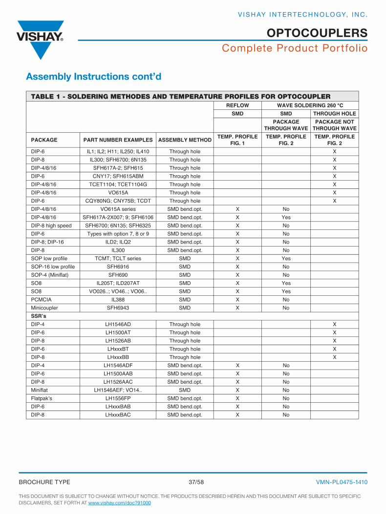
Complete Product Portfolio
THIS DOCUMENT IS SUBJECT TO CHANGE WITHOUT NOTICE. THE PRODUCTS DESCRIBED HEREIN AND THIS DOCUMENT ARE SUBJECT TO SPECIFIC DISCLAIMERS, SET FORTH AT www.vishay.com/doc?91000
VMN-PL0475-141037/58BROCHURE TyPE
OpTOCOupLErS
V I S H AY I N T E R T E C H N O LO GY, I N C .
www.vishay.com For technical questions, contact: [email protected] Document Number: 80054122 Rev. 1.6, 24-Nov-08
Assembly InstructionsVishay Semiconductors Assembly Instructions
TABLE 1 - SOLDERING METHODES AND TEMPERATURE PROFILES FOR OPTOCOUPLER REFLOW WAVE SOLDERING 260 °C
SMD SMD THROUGH HOLEPACKAGE
THROUGH WAVEPACKAGE NOT
THROUGH WAVE
PACKAGE PART NUMBER EXAMPLES ASSEMBLY METHOD TEMP. PROFILEFIG. 1
TEMP. PROFILEFIG. 2
TEMP. PROFILEFIG. 2
X eloh hguorhT014LI ;052LI ;11H ;2LI ;1LI 6-PID X eloh hguorhT531N6 ;0076HFS ;003LI 8-PID X eloh hguorhT516HFS ;2-A716HFS 61/8/4-PID X eloh hguorhTMBA516HFS ;71YNC 6-PID X eloh hguorhTG4011TECT ;4011TECT 61/8/4-PID X eloh hguorhTA516OV 61/8/4-PID X eloh hguorhTTDCT ;B57YNC ;GN08YQC 6-PID
DIP-4/8/16 VO615A series SMD bend.opt. X No DIP-4/8/16 SFH617A-2X007; 9; SFH6106 SMD bend.opt. X Yes DIP-8 high speed SFH6700; 6N135; SFH6325 SMD bend.opt. X No DIP-6 Types with option 7, 8 or 9 SMD bend.opt. X No DIP-8; DIP-16 ILD2; ILQ2 SMD bend.opt. X No
oN X .tpo.dneb DMS003LI 8-PIDSOP low profile TCMT; TCLT series SMD X Yes SOP-16 low profile SFH6916 SMD X No SOP-4 (Miniflat) SFH690 SMD X No
seY X DMSTA702DLI ;T502LI 8OSSO8 VO026..; VO46..; VO06.. SMD X Yes
oN X DMS 883LI AICMCPMinicoupler SFH6943 SMD X No SSR’s
X eloh hguorhTDA6451HL 4-PID X eloh hguorhTTA0051HL 6-PID X eloh hguorhTBA6251HL 8-PID X eloh hguorhTTBxxxHL 6-PID X eloh hguorhTBBxxxHL 8-PID
oN X .tpo.dneb DMSFDA6451HL 4-PID oN X .tpo.dneb DMSBAA0051HL 6-PID oN X .tpo.dneb DMSCAA6251HL 8-PID
Miniflat LH1546AEF; VO14.. SMD X No Flatpak’s LH1556FP SMD bend.opt. X No
oN X .tpo.dneb DMSBABxxxHL 6-PID oN X .tpo.dneb DMSCABxxxHL 8-PID
Assembly Instructions cont’d
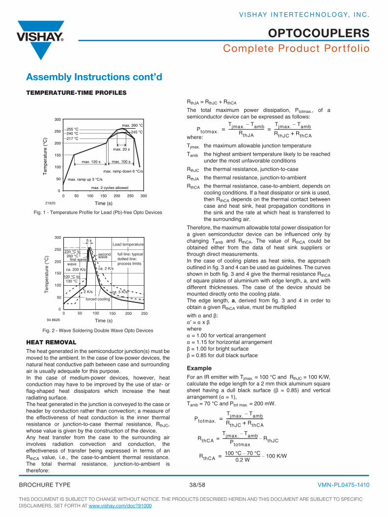
Complete Product Portfolio
THIS DOCUMENT IS SUBJECT TO CHANGE WITHOUT NOTICE. THE PRODUCTS DESCRIBED HEREIN AND THIS DOCUMENT ARE SUBJECT TO SPECIFIC DISCLAIMERS, SET FORTH AT www.vishay.com/doc?91000
VMN-PL0475-141038/58BROCHURE TyPE
OpTOCOupLErS
V I S H AY I N T E R T E C H N O LO GY, I N C .
Assembly Instructions cont’d
Document Number: 80054 For technical questions, contact: [email protected] www.vishay.comRev. 1.6, 24-Nov-08 123
Assembly InstructionsAssembly Instructions Vishay Semiconductors
TEMPERATURE-TIME PROFILES
Fig. 1 - Temperature Profile for Lead (Pb)-free Opto Devices
Fig. 2 - Wave Soldering Double Wave Opto Devices
HEAT REMOVALThe heat generated in the semiconductor junction(s) must bemoved to the ambient. In the case of low-power devices, thenatural heat conductive path between case and surroundingair is usually adequate for this purpose.In the case of medium-power devices, however, heatconduction may have to be improved by the use of star- orflag-shaped heat dissipators which increase the heatradiating surface.The heat generated in the junction is conveyed to the case orheader by conduction rather than convection; a measure ofthe effectiveness of heat conduction is the inner thermalresistance or junction-to-case thermal resistance, RthJC,whose value is given by the construction of the device.Any heat transfer from the case to the surrounding airinvolves radiation convection and conduction, theeffectiveness of transfer being expressed in terms of anRthCA value, i.e., the case-to-ambient thermal resistance.The total thermal resistance, junction-to-ambient istherefore:
RthJA = RthJC + RthCA
The total maximum power dissipation, Ptotmax., of asemiconductor device can be expressed as follows:
where:Tjmax. the maximum allowable junction temperatureTamb the highest ambient temperature likely to be reached
under the most unfavorable conditionsRthJC the thermal resistance, junction-to-caseRthJA the thermal resistance, junction-to-ambientRthCA the thermal resistance, case-to-ambient, depends on
cooling conditions. If a heat dissipator or sink is used,then RthCA depends on the thermal contact betweencase and heat sink, heat propagation conditions inthe sink and the rate at which heat is transferred tothe surrounding air.
Therefore, the maximum allowable total power dissipation fora given semiconductor device can be influenced only bychanging Tamb and RthCA. The value of RthCA could beobtained either from the data of heat sink suppliers orthrough direct measurements.In the case of cooling plates as heat sinks, the approachoutlined in fig. 3 and 4 can be used as guidelines. The curvesshown in both fig. 3 and 4 give the thermal resistance RthCAof square plates of aluminium with edge length, a, and withdifferent thicknesses. The case of the device should bemounted directly onto the cooling plate.The edge length, a, derived from fig. 3 and 4 in order toobtain a given RthCA value, must be multipliedwith α and β:α ' = α x βwhereα = 1.00 for vertical arrangementα = 1.15 for horizontal arrangementβ = 1.00 for bright surfaceβ = 0.85 for dull black surface
ExampleFor an IR emitter with Tjmax. = 100 °C and RthJC = 100 K/W,calculate the edge length for a 2 mm thick aluminum squaresheet having a dull black surface (β = 0.85) and verticalarrangement (α = 1),Tamb = 70 °C and Ptot max. = 200 mW.
0
50
100
150
200
250
300
0 50 100 150 200 250 300
Time (s)
Tem
pera
ture
(°C
)
255 °C240 °C 245 °C
max. 260 °C
max. 120 s max. 100 s
217 °C
max. 20 s
max. ramp up 3 °C/s
max. ramp down 6 °C/s
max. 2 cycles allowed
21620
2 K/s
secondwavefirst wavewave
ca. 5 K/s
5 s
full line: typicaldotted line:process limits
Time (s)
Tem
pera
ture
(°C
)
300
250
200
150
100
50
00 50 100 150 200 250
94 8626
Lead temperature
235 °C to 260 °C
100 °C to 130 °C
ca. 200 K/s
forced cooling
ca. 2 K/s
Ptotmax.Tjmax. Tamb–
RthJA---------------------------------------
Tjmax. Tamb–RthJC RthCA+-----------------------------------------= =
Ptotmax.Tjmax. Tamb–RthJC RthCA+-------------------------------------=
RthCATjmax. Tamb–
Ptotmax--------------------------------------- RthJC–=
RthCA100 °C 70 °C–
0.2 W--------------------------------------- 100 K/W–=

Complete Product Portfolio
THIS DOCUMENT IS SUBJECT TO CHANGE WITHOUT NOTICE. THE PRODUCTS DESCRIBED HEREIN AND THIS DOCUMENT ARE SUBJECT TO SPECIFIC DISCLAIMERS, SET FORTH AT www.vishay.com/doc?91000
VMN-PL0475-141039/58BROCHURE TyPE
OpTOCOupLErS
V I S H AY I N T E R T E C H N O LO GY, I N C .
www.vishay.com For technical questions, contact: [email protected] Document Number: 80054124 Rev. 1.6, 24-Nov-08
Assembly InstructionsVishay Semiconductors Assembly Instructions
can be calculated from the relationship:
Fig. 3
With RthCA = 50 k/W and ΔT = 10 °C, a plate of 2 mmthickness has an edge length α = 28 µ.
Fig. 4
However, equipment life and reliability have to be taken intoconsideration and therefore a larger sink would normally beused to avoid operating the devices continuously at theirmaximum permissible junction temperature.
RthCA30
0.2 ---------- 100 K/W–=
RthCA 50 K/W=
ΔT Tcase Tamb–=
Ptotmax.Tjmax. Tamb–RthJC RthCA+-------------------------------------
Tcase Tamb–RthCA
----------------------------------= =
ΔT Tcase Tamb–RthCA Tjmax. Tamb–( )
RthJC RthCA+--------------------------------------------------------------= =
ΔT 50 K/W 100 °C 70 °C–×150 K/W
-----------------------------------------------------------------=
ΔT 50 K/W 30 °C×150 K/W
-------------------------------------------=
ΔT 10 °C 10 K= =
10 1001
10
100
Rth
CA (
K/W
)
a (mm)1000
∆T = 10 °C
30 °C60 °C120 °C
Plate thickness: 0.5 mm
94 7834
10 1001
10
100
Rth
CA (
K/W
)
a (mm)1000
Plate thickness: 2 mm
∆T = 10 °C
30 °C60 °C120 °C
94 7835
Assembly Instructions cont’d

Complete Product Portfolio
THIS DOCUMENT IS SUBJECT TO CHANGE WITHOUT NOTICE. THE PRODUCTS DESCRIBED HEREIN AND THIS DOCUMENT ARE SUBJECT TO SPECIFIC DISCLAIMERS, SET FORTH AT www.vishay.com/doc?91000
VMN-PL0475-141040/58BROCHURE TyPE
OpTOCOupLErS
V I S H AY I N T E R T E C H N O LO GY, I N C .
Packaging, Tape and Reel Informationwww.vishay.com Vishay Semiconductors
Rev. 2.2, 06-Oct-11 1 Document Number: 83714
For technical questions, contact: [email protected] DOCUMENT IS SUBJECT TO CHANGE WITHOUT NOTICE. THE PRODUCTS DESCRIBED HEREIN AND THIS DOCUMENT
ARE SUBJECT TO SPECIFIC DISCLAIMERS, SET FORTH AT www.vishay.com/doc?91000
Packaging, Tape and Reel Information
DESCRIPTIONOptocouplers are available in plastic dual-in-line packages (DIP), SOP packages, and in a surface-mount, gull-wing, lead bend configuration. Optocouplers purchased in the DIP configuration are shipped in tubes. Optocouplers purchased in a gull-wing configuration can be shipped in tubes or on carrier tape. This section provides stick specifications, tape and reel specifications, and component information.
TUBE SPECIFICATIONSFigure 1 shows the physical dimensions of transparent, antistatic, plastic shipping tubes. Figure 2 shows tube safety agency labeling and orientation information.
The following table lists the number of parts per tube.
Fig. 1 - Shipping Tube Specifications for DIP Packages
DEVICE PER TUBETYPE UNITS/TUBE TUBES/BOX UNITS/BOX
DIP-16 25 40 1000
DIP-4 100 40 4000
DIP-6 50 40 2000
DIP-8 50 40 2000
HV, CNY64 40 50 2000
HV, CNY65 30 35 1050
HV, CNY66 25 35 875
MADE IN MALAYSIAANTISTATIC
Detail A
200 ± 0.5
125 ± 0.5
150 ± 0.5
Detail B
Detail A Detail B10°
6°
Section A - B
B
R0.1
R 0.5
14 x
// 0.2 B
13 x 10 = 130
A
B
– 1.0
Not to scale
Transparent rigid PVC
A
Dimensions in millimeters
17996
OPTOSEMICONDUCTOR VISHAY
260 ± 0.5330 ± 0.5
528 ± 0.2
30 ± 0.5
0.7 ± 0.5
3 ± 0.5380 ± 1
12 ± 0.3
6.6 ± 0.3
4.4 ± 0.3
5.7 ± 0.15
11 ± 0.3
0.6 ± 0.1
2.7 ± 0.2
– 1.0
1.0
– 1.0
– 1.0
packaging Information
Packaging, Tape and Reel Informationwww.vishay.com Vishay Semiconductors
Rev. 2.2, 06-Oct-11 2 Document Number: 83714
For technical questions, contact: [email protected] DOCUMENT IS SUBJECT TO CHANGE WITHOUT NOTICE. THE PRODUCTS DESCRIBED HEREIN AND THIS DOCUMENT
ARE SUBJECT TO SPECIFIC DISCLAIMERS, SET FORTH AT www.vishay.com/doc?91000
Fig. 2 - Shipping Tube Specifications for SOP Packages
TUBE SPECIFICATIONS FOR DIP AND HIGH ISOLATION VOLTAGE PACKAGES
Fig. 3 - DIP-6 N, G Fig. 4 - DIP-4, -2, -16 N, G
Side viewscale: 4X
Top viewnot to scale
4 (100)
0.312 ref.(7.8 ref.)
Dimensions in inches (millimeters)
17997
OPTOSEMICONDUCTOR ANTISTATICVISHAY
0.46 ± 0.01(11.5 ± 0.25)0.344 ± 0.01(8.6 ± 0.25)
0.058 ± 0.008(1.46 ± 0.19)
0.03 ± 0.005(0.7 ± 0.13)
0.104 ± 0.01(2.6 ± 0.25)
0.03 ± 0.01(0.7 ± 0.25)
22.4 ± 0.04
(558.8 ± 1)
15912 15915

Complete Product Portfolio
THIS DOCUMENT IS SUBJECT TO CHANGE WITHOUT NOTICE. THE PRODUCTS DESCRIBED HEREIN AND THIS DOCUMENT ARE SUBJECT TO SPECIFIC DISCLAIMERS, SET FORTH AT www.vishay.com/doc?91000
VMN-PL0475-141041/58BROCHURE TyPE
OpTOCOupLErS
V I S H AY I N T E R T E C H N O LO GY, I N C .
Packaging, Tape and Reel Informationwww.vishay.com Vishay Semiconductors
Rev. 2.2, 06-Oct-11 3 Document Number: 83714
For technical questions, contact: [email protected] DOCUMENT IS SUBJECT TO CHANGE WITHOUT NOTICE. THE PRODUCTS DESCRIBED HEREIN AND THIS DOCUMENT
ARE SUBJECT TO SPECIFIC DISCLAIMERS, SET FORTH AT www.vishay.com/doc?91000
Fig. 5 - CNY64
Fig. 6 - CNY65, 66
TAPE AND REEL SPECIFICATIONSSurface-mounted devices are packaged in embossed tape and wound onto 13" molded plastic reels for shipment, to comply with Electronics Industries Association Standard EIA-481, revision A, and International Electrotechnical Commission standard IEC 60286.
Leaders and Trailers
The carrier tape and cover tape are not spliced. Both tapes are one single uninterrupted piece from end to end, as shown in figure 2. Both ends of the tape have empty pockets meeting these requirements.
• Trailer end (inside hub of reel) is 200 mm minimum
• Leader end (outside of reel) is 400 mm minimum and 560 mm maximum
• Unfilled leader and trailer pockets are sealed
• Leaders and trailers are taped to tape and hub, respectively, with masking tape
• All materials are static-dissipative
Fig. 7 - Tape and Reel Shipping Medium
REELS• As shown in figure 4, all reels contain standard areas for
the placement of ESD stickers and labels. Each reel also has a tape slot in its core. The overall reel dimension is 13". Reels contain 1000 6 or 8 pin gullwing parts and could have up to three inspection lots
Fig. 8 - Tape and Reel Shipping Medium
15913
15914
Top cover tape
EmbossmentEmbossed carrier
17998
ESD sticker
Tape slotin core
330(13")
Regular, specialor bar code label
17999
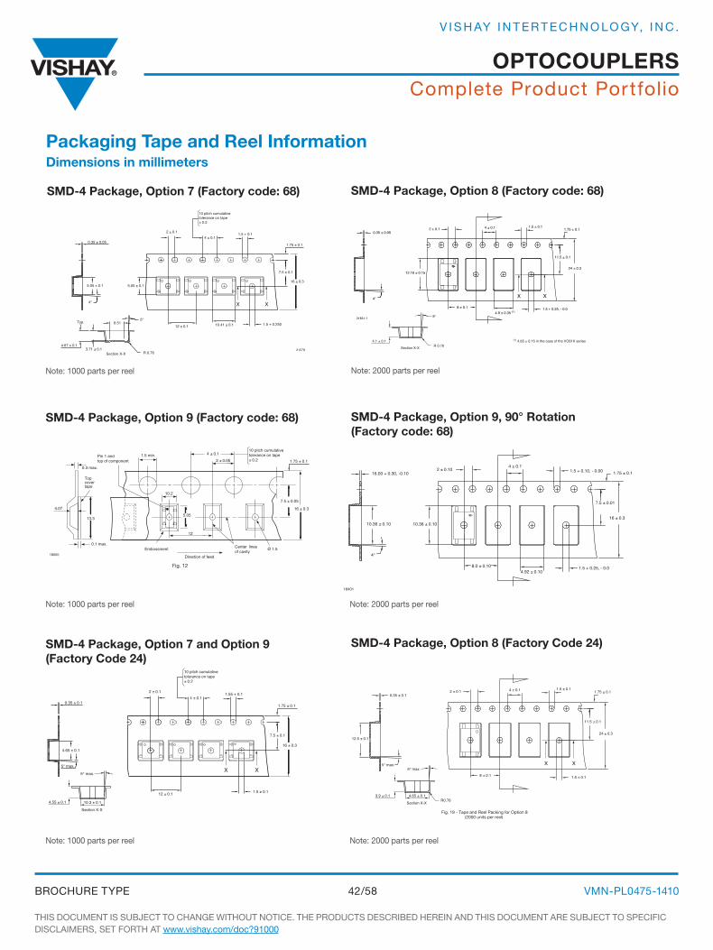
Complete Product Portfolio
THIS DOCUMENT IS SUBJECT TO CHANGE WITHOUT NOTICE. THE PRODUCTS DESCRIBED HEREIN AND THIS DOCUMENT ARE SUBJECT TO SPECIFIC DISCLAIMERS, SET FORTH AT www.vishay.com/doc?91000
VMN-PL0475-141042/58BROCHURE TyPE
OpTOCOupLErS
V I S H AY I N T E R T E C H N O LO GY, I N C .
packaging Tape and reel Information Dimensions in millimeters
Packaging, Tape and Reel Informationwww.vishay.com Vishay Semiconductors
Rev. 2.2, 06-Oct-11 5 Document Number: 83714
For technical questions, contact: [email protected] DOCUMENT IS SUBJECT TO CHANGE WITHOUT NOTICE. THE PRODUCTS DESCRIBED HEREIN AND THIS DOCUMENT
ARE SUBJECT TO SPECIFIC DISCLAIMERS, SET FORTH AT www.vishay.com/doc?91000
TAPE AND REEL PACKAGING FOR SMD-4 OPTOCOUPLERS WITH OPTION 7Dimensions in millimeters
Selected 4 pin optocouplers are available in tape and reel format. To order a 4 pin optocoupler with option 7 on tape and reel, add a suffix “T” after the part number, SFH615A-3X007T.
The tape is 16 mm and is wound on a 33 cm reel. There are 1000 parts per reel. Taped and reeled 4 pin optocouplers conform to EIA-481-2 and IEC 60286-3.
Fig. 11
TAPE AND REEL PACKAGING FOR SMD-4 OPTOCOUPLERS WITH OPTION 9Dimensions in millimeters
Selected 4 pin optocouplers are available in tape and reel format. To order any SFH6xx6 optocoupler on tape and reel, add suffix “T” after the part number, i.e., SFH6156-3T.
The tape is 16 mm and is wound on a 33 cm reel. There are 1000 parts per reel. Taped and reeled 4 pin optocouplers conform to EIA-481-2 and IEC60286-3.
Fig. 12
2 ± 0.14 ± 0.1
1.5 + 0.1
1.75 ± 0.1
16 ± 0.3
7.5 ± 0.1
1.5 + 0.25010.41 ± 0.112 ± 0.1
5.05 ± 0.15.05 ± 0.1
0.35 ± 0.05
Typ.
4°
5°
R 0.763.71 ± 0.1
4.67 ± 0.1
6.51
21579
10 pitch cumulative tolerance on tape ± 0.2
XX
Section X-X
Ø 1.5
13.3
4.07
0.3 max.
0.1 max.
16 ± 0.3
18005
4 ± 0.12 ± 0.05
10.2
5.05
12
7.5 ± 0.05
Embossment
Direction of feed
Center linesof cavity
10 pitch cumulative tolerance on tape ± 0.2
1.5 min.Pin 1 and top of component
Topcovertape
1.75 ± 0.1
SMD-4 package, Option 7 (Factory code: 68)
SMD-4 package, Option 9, 90° rotation (Factory code: 68)
SMD-4 package, Option 9 (Factory code: 68)
SMD-4 package, Option 7 and Option 9 (Factory Code 24)
SMD-4 package, Option 8 (Factory Code 24)
SMD-4 package, Option 8 (Factory code: 68)
Note: 1000 parts per reel
Note: 1000 parts per reel
Note: 1000 parts per reel
Note: 2000 parts per reel
Note: 2000 parts per reel
Note: 2000 parts per reel
Packaging, Tape and Reel Informationwww.vishay.com Vishay Semiconductors
Rev. 2.2, 06-Oct-11 5 Document Number: 83714
For technical questions, contact: [email protected] DOCUMENT IS SUBJECT TO CHANGE WITHOUT NOTICE. THE PRODUCTS DESCRIBED HEREIN AND THIS DOCUMENT
ARE SUBJECT TO SPECIFIC DISCLAIMERS, SET FORTH AT www.vishay.com/doc?91000
TAPE AND REEL PACKAGING FOR SMD-4 OPTOCOUPLERS WITH OPTION 7Dimensions in millimeters
Selected 4 pin optocouplers are available in tape and reel format. To order a 4 pin optocoupler with option 7 on tape and reel, add a suffix “T” after the part number, SFH615A-3X007T.
The tape is 16 mm and is wound on a 33 cm reel. There are 1000 parts per reel. Taped and reeled 4 pin optocouplers conform to EIA-481-2 and IEC 60286-3.
Fig. 11
TAPE AND REEL PACKAGING FOR SMD-4 OPTOCOUPLERS WITH OPTION 9Dimensions in millimeters
Selected 4 pin optocouplers are available in tape and reel format. To order any SFH6xx6 optocoupler on tape and reel, add suffix “T” after the part number, i.e., SFH6156-3T.
The tape is 16 mm and is wound on a 33 cm reel. There are 1000 parts per reel. Taped and reeled 4 pin optocouplers conform to EIA-481-2 and IEC60286-3.
Fig. 12
2 ± 0.14 ± 0.1
1.5 + 0.1
1.75 ± 0.1
16 ± 0.3
7.5 ± 0.1
1.5 + 0.25010.41 ± 0.112 ± 0.1
5.05 ± 0.15.05 ± 0.1
0.35 ± 0.05
Typ.
4°
5°
R 0.763.71 ± 0.1
4.67 ± 0.1
6.51
21579
10 pitch cumulative tolerance on tape ± 0.2
XX
Section X-X
Ø 1.5
13.3
4.07
0.3 max.
0.1 max.
16 ± 0.3
18005
4 ± 0.12 ± 0.05
10.2
5.05
12
7.5 ± 0.05
Embossment
Direction of feed
Center linesof cavity
10 pitch cumulative tolerance on tape ± 0.2
1.5 min.Pin 1 and top of component
Topcovertape
1.75 ± 0.1
Packaging, Tape and Reel Informationwww.vishay.com Vishay Semiconductors
Rev. 2.2, 06-Oct-11 6 Document Number: 83714
For technical questions, contact: [email protected] DOCUMENT IS SUBJECT TO CHANGE WITHOUT NOTICE. THE PRODUCTS DESCRIBED HEREIN AND THIS DOCUMENT
ARE SUBJECT TO SPECIFIC DISCLAIMERS, SET FORTH AT www.vishay.com/doc?91000
TAPE AND REEL PACKAGING FOR SMD-4 OPTOCOUPLERS WITH OPTION 9, 90° ROTATIONDimensions in millimeters (inches)
Selected 4 pin optocouplers are available in tape and reel format. To order any SFH6xx series optocoupler on tape and reel with this orientation, add suffix “T1” after the part number, i.e., SFH6156-5T1.
The tape is 16 mm and is wound on a 33 cm reel. There are 2000 parts per reel. Taped and reeled 4 pin optocouplers conform to EIA-481-2 and IEC 60286-3.
Fig. 13
TAPE AND REEL PACKAGING FOR SMD-4 OPTOCOUPLERS WITH OPTION 8Dimensions in millimeters
Selected 4 pin optocouplers are available in tape and reel format. To order any SFH6xx series optocoupler on tape and reel, add suffix “T” after the part number, i.e., SFH615A-4X018T.
The tape is 24 mm and is wound on a 33 cm reel. There are 2000 parts per reel. Taped and reeled 4 pin optocouplers conform to EIA-481-2 and IEC 60286-3.
Fig. 14
16 ± 0.3 (0.630 ± 0.012)
4°
16.00 + 0.30, -0.10 (0.013 (0.0008), -0.0004)
18401
4 ± 0.1(0.157 ± 0.004) 1.5 + 0.10, - 0.00
(0.59 ± 0.004)
1.75 ± 0.1(0.069 ± 0.004)
7.5 ± 0.01(0.295 ± 0.004)
2 ± 0.10(0.079 ± 0.004)
8.0 ± 0.10(0.315 + 0.004)
10.36 ± 0.100.408 ± 0.004
10.36 ± 0.100.408 ± 0.004
4.92 ± 0.100.194 ± 0.004
1.5 + 0.25, - 0.00.059 + 0.001, - 0.0
24 ± 0.3
4°
21831-1
4 ± 0.1 1.75 ± 0.1
11.5 ± 0.1
2 ± 0.1
8 ± 0.1
12.10 ± 0.15
4.9 ± 0.35 (1)1.5 + 0.25, - 0.0
0.35 ± 0.05
1.5 ± 0.1
XX
8°
R 0.764.1 ± 0.1
Section X-X
(1) 4.65 ± 0.15 in the case of the VO61X series
Packaging, Tape and Reel Informationwww.vishay.com Vishay Semiconductors
Rev. 2.2, 06-Oct-11 6 Document Number: 83714
For technical questions, contact: [email protected] DOCUMENT IS SUBJECT TO CHANGE WITHOUT NOTICE. THE PRODUCTS DESCRIBED HEREIN AND THIS DOCUMENT
ARE SUBJECT TO SPECIFIC DISCLAIMERS, SET FORTH AT www.vishay.com/doc?91000
TAPE AND REEL PACKAGING FOR SMD-4 OPTOCOUPLERS WITH OPTION 9, 90° ROTATIONDimensions in millimeters (inches)
Selected 4 pin optocouplers are available in tape and reel format. To order any SFH6xx series optocoupler on tape and reel with this orientation, add suffix “T1” after the part number, i.e., SFH6156-5T1.
The tape is 16 mm and is wound on a 33 cm reel. There are 2000 parts per reel. Taped and reeled 4 pin optocouplers conform to EIA-481-2 and IEC 60286-3.
Fig. 13
TAPE AND REEL PACKAGING FOR SMD-4 OPTOCOUPLERS WITH OPTION 8Dimensions in millimeters
Selected 4 pin optocouplers are available in tape and reel format. To order any SFH6xx series optocoupler on tape and reel, add suffix “T” after the part number, i.e., SFH615A-4X018T.
The tape is 24 mm and is wound on a 33 cm reel. There are 2000 parts per reel. Taped and reeled 4 pin optocouplers conform to EIA-481-2 and IEC 60286-3.
Fig. 14
16 ± 0.3
4°
16.00 + 0.30, -0.10
18401
4 ± 0.11.5 + 0.10, - 0.00 1.75 ± 0.1
7.5 ± 0.01
2 ± 0.10
8.0 ± 0.10
10.36 ± 0.10 10.36 ± 0.10
4.92 ± 0.101.5 + 0.25, - 0.0
24 ± 0.3
4°
21831-1
4 ± 0.1 1.75 ± 0.1
11.5 ± 0.1
2 ± 0.1
8 ± 0.1
12.10 ± 0.15
4.9 ± 0.35 (1)1.5 + 0.25, - 0.0
0.35 ± 0.051.5 ± 0.1
XX
8°
R 0.764.1 ± 0.1
Section X-X
(1) 4.65 ± 0.15 in the case of the VO61X series
2 ± 0.14 ± 0.1
1.75 ± 0.1
16 ± 0.3
7.5 ± 0.1
1.5 ± 0.112 ± 0.1
4.65 ± 0.1
0.35 ± 0.1
5° max.
10 pitch cumulative tolerance on tape ± 0.2
XX5° max.
4.55 ± 0.1
Section X-X
10.3 ± 0.1
1.55 + 0.1
Fig. 19 - Tape and Reel Packing for Option 8(2000 units per reel)
24 ± 0.3
5° max.
4 ± 0.1 1.75 ± 0.1
11.5 ± 0.1
2 ± 0.1
8 ± 0.1
12.5 ± 0.1
1.5 ± 0.1
0.35 ± 0.11.5 ± 0.1
XX5° max.
R0.763.9 ± 0.1
Section X-X
4.65 ± 0.1
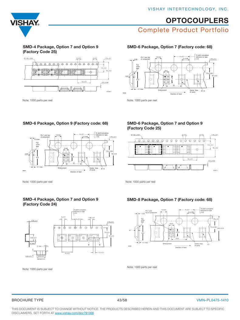
Complete Product Portfolio
THIS DOCUMENT IS SUBJECT TO CHANGE WITHOUT NOTICE. THE PRODUCTS DESCRIBED HEREIN AND THIS DOCUMENT ARE SUBJECT TO SPECIFIC DISCLAIMERS, SET FORTH AT www.vishay.com/doc?91000
VMN-PL0475-141043/58BROCHURE TyPE
OpTOCOupLErS
V I S H AY I N T E R T E C H N O LO GY, I N C .
Packaging, Tape and Reel Informationwww.vishay.com Vishay Semiconductors
Rev. 2.2, 06-Oct-11 8 Document Number: 83714
For technical questions, contact: [email protected] DOCUMENT IS SUBJECT TO CHANGE WITHOUT NOTICE. THE PRODUCTS DESCRIBED HEREIN AND THIS DOCUMENT
ARE SUBJECT TO SPECIFIC DISCLAIMERS, SET FORTH AT www.vishay.com/doc?91000
TAPE AND REEL PACKAGING FOR SMD-8 OPTOCOUPLERS WITH OPTION 7Dimensions in millimeters (inches)
Selected 8 pin optocouplers with option 9 are available in tape and reel format. To order 8 pin optocoupler with option 7 on tape and reel, add a suffix “T” after the option, i.e., ILCT6-X007T.
The tape is 16 mm and is wound on a 33 cm reel. There are 1000 parts per reel. Taped and reeled 8-pin optocouplers conform to EIA-481-2 and IEC 60286-3.
Fig. 17
TAPE AND REEL PACKAGING FOR SMD-8 OPTOCOUPLERS WITH OPTION 9Dimensions in millimeters (inches)
Selected 8-pin optocouplers with option 9 are available in tape and reel format. To order 8 pin optocoupler with option 9 on tape and reel, add a suffix “T” after the option, i.e., ILCT6-X009T.
The tape is 16 mm and is wound on a 33 cm reel. There are 1000 parts per reel. Taped and reeled 8 pin optocouplers conform to EIA-481-2 and IEC 60286-3.
Fig. 18
1.75 ± 0.1
13.3
4.7
0.35
16.0 ± 0.3
18008
4 ± 0.12 ± 0.05
10.41
10.21
12.0
7.5 ± 0.05
Embossment
Direction of feed
Center linesof cavity
10 pitch cumulative tolerance on tape ± 0.2
1.5 min.
1.5
Pin 1 and top of component
Topcovertape
0.1 max.
4.17
18009
10.2
10.31
12.0
1.75 ± 0.1
13.3
0.35
16.0 ± 0.3
4 ± 0.12 ± 0.05
7.5 ± 0.05
Embossment
Direction of feed
Center linesof cavity
10 pitch cumulative tolerance on tape ± 0.2
1.5 min.
1.5
Pin 1 and top of component
Topcovertape
0.1 max.
SMD-8 package, Option 7 (Factory code: 68)
Note: 1000 parts per reel
Note: 1000 parts per reelNote: 1000 parts per reel
Note: 1000 parts per reel Note: 1000 parts per reel
Note: 1000 parts per reel
Packaging, Tape and Reel Informationwww.vishay.com Vishay Semiconductors
Rev. 2.2, 06-Oct-11 7 Document Number: 83714
For technical questions, contact: [email protected] DOCUMENT IS SUBJECT TO CHANGE WITHOUT NOTICE. THE PRODUCTS DESCRIBED HEREIN AND THIS DOCUMENT
ARE SUBJECT TO SPECIFIC DISCLAIMERS, SET FORTH AT www.vishay.com/doc?91000
TAPE AND REEL PACKAGING FOR SMD-6 OPTOCOUPLERS WITH OPTION 7Dimensions in millimeters
Selected 6 pin optocouplers with option 7 are available in tape and reel format. To order 6 pin optocoupler with option 7 on tape and reel, add a suffix “T” after the option, i.e., CNY17-3X007T.
The tape is 16 mm and is wound on a 33 cm reel. There are 1000 parts per reel. Taped and reeled 6 pin optocouplers conform to EIA-481-2 and IEC 60286-3.
Fig. 15
TAPE AND REEL PACKAGING FOR SMD-6 OPTOCOUPLERS WITH OPTION 9Dimensions in millimeters
Selected 6 pin optocouplers with option 9 are available in tape and reel format. To order 6 pin optocoupler with option 9 on tape and reel, add a suffix “T” after the option, i.e., CNY17-3X009T.
The tape is 16 mm and is wound on a 33 cm reel. There are 1000 parts per reel. Taped and reeled 6 pin optocouplers conform to EIA-481-2 and IEC 60286-3.
Fig. 16
Embossment
Direction of feed
Center linesof cavity
10 pitch cumulativetolerance on tape± 0.2
1.5 min.
Ø 1.5
Pin 1 and topof component
Topcovertape
13.3
4.57
0.35
0.1 max.
16 ± 0.3
18006
4 ± 0.1
2 ± 0.05
10.4
9
12
7.5 ± 0.05
1.75 ± 0.1
Embossment
Direction of feed
Center linesof cavity
10 pitch cumulativetolerance on tape± 0.2
1.5 min.
Ø 1.5
Pin 1 and topof component
Topcovertape
13.3
4.09
0.3 max.
0.1 max.
16 ± 0.3
18007
4 ± 0.1
2 ± 0.05
10.35
9.14
12
7.5 ± 0.05
1.75 ± 0.1
SMD-6 package, Option 7 (Factory code: 68)SMD-4 package, Option 7 and Option 9 (Factory Code 25)
SMD-6 package, Option 9 (Factory code: 68)
SMD-4 package, Option 7 and Option 9 (Factory Code 24)
SMD-6 package, Option 7 and Option 9 (Factory Code 25)
Fig. 19 - Tape and Packing for Option 7 and Option 9
22536-2
Ø 1.55 ± 0.05 1.75 ± 0.1
7.5 ± 0.1
16 ± 0.3
0.3 ± 0.05
2 ± 0.1 4 ± 0.1
12 ± 0.1
Fig. 15 - Tape and Reel Drawing, 1000 Units per Reel
22537-1
Ø 1.55 ± 0.05 1.75 ± 0.1
12 ± 0.10.3 ± 0.05
2 ± 0.1 4 ± 0.1
7.5 ± 0.1
16 ± 0.3
Fig. 18 - Tape and Reel Packing for Option 7 and Option 9(1000 units per reel)
2 ± 0.14 ± 0.1
1.75 ± 0.1
16 ± 0.3
7.5 ± 0.1
1.5 ± 0.112 ± 0.1
4.65 ± 0.1
0.35 ± 0.1
5° max.
10 pitch cumulative tolerance on tape ± 0.2
XX5° max.
4.55 ± 0.1
Section X-X
10.3 ± 0.1
1.55 + 0.1

Complete Product Portfolio
THIS DOCUMENT IS SUBJECT TO CHANGE WITHOUT NOTICE. THE PRODUCTS DESCRIBED HEREIN AND THIS DOCUMENT ARE SUBJECT TO SPECIFIC DISCLAIMERS, SET FORTH AT www.vishay.com/doc?91000
VMN-PL0475-141044/58BROCHURE TyPE
OpTOCOupLErS
V I S H AY I N T E R T E C H N O LO GY, I N C .
SMD-8 package, Option 7 and Option 9 (Factory code: 68)
SMD-8 package, Option 7 (Factory Code 28)
Note: 1000 parts per reel
Note: 750 parts per reel
2000 parts per reel
Note: 1000 parts per reel
Packaging, Tape and Reel Informationwww.vishay.com Vishay Semiconductors
Rev. 2.2, 06-Oct-11 8 Document Number: 83714
For technical questions, contact: [email protected] DOCUMENT IS SUBJECT TO CHANGE WITHOUT NOTICE. THE PRODUCTS DESCRIBED HEREIN AND THIS DOCUMENT
ARE SUBJECT TO SPECIFIC DISCLAIMERS, SET FORTH AT www.vishay.com/doc?91000
TAPE AND REEL PACKAGING FOR SMD-8 OPTOCOUPLERS WITH OPTION 7Dimensions in millimeters (inches)
Selected 8 pin optocouplers with option 9 are available in tape and reel format. To order 8 pin optocoupler with option 7 on tape and reel, add a suffix “T” after the option, i.e., ILCT6-X007T.
The tape is 16 mm and is wound on a 33 cm reel. There are 1000 parts per reel. Taped and reeled 8-pin optocouplers conform to EIA-481-2 and IEC 60286-3.
Fig. 17
TAPE AND REEL PACKAGING FOR SMD-8 OPTOCOUPLERS WITH OPTION 9Dimensions in millimeters (inches)
Selected 8-pin optocouplers with option 9 are available in tape and reel format. To order 8 pin optocoupler with option 9 on tape and reel, add a suffix “T” after the option, i.e., ILCT6-X009T.
The tape is 16 mm and is wound on a 33 cm reel. There are 1000 parts per reel. Taped and reeled 8 pin optocouplers conform to EIA-481-2 and IEC 60286-3.
Fig. 18
1.75 ± 0.1
13.3
4.7
0.35
16.0 ± 0.3
18008
4 ± 0.12 ± 0.05
10.41
10.21
12.0
7.5 ± 0.05
Embossment
Direction of feed
Center linesof cavity
10 pitch cumulative tolerance on tape ± 0.2
1.5 min.
1.5
Pin 1 and top of component
Topcovertape
0.1 max.
4.17
18009
10.2
10.31
12.0
1.75 ± 0.1
13.3
0.35
16.0 ± 0.3
4 ± 0.12 ± 0.05
7.5 ± 0.05
Embossment
Direction of feed
Center linesof cavity
10 pitch cumulative tolerance on tape ± 0.2
1.5 min.
1.5
Pin 1 and top of component
Topcovertape
0.1 max.
Fig. 19 - Reel Dimensions (1000 units per reel)
Packaging, Tape and Reel Informationwww.vishay.com Vishay Semiconductors
Rev. 2.2, 06-Oct-11 9 Document Number: 83714
For technical questions, contact: [email protected] DOCUMENT IS SUBJECT TO CHANGE WITHOUT NOTICE. THE PRODUCTS DESCRIBED HEREIN AND THIS DOCUMENT
ARE SUBJECT TO SPECIFIC DISCLAIMERS, SET FORTH AT www.vishay.com/doc?91000
TAPE AND REEL PACKAGING FOR SMD-16 OPTOCOUPLERS WITH OPTION 7Dimensions in millimeters (inches)
Selected 16 pin optocouplers with option 7 are available in tape and reel format. To order 16 pin optocoupler with option 7 on tape and reel, add a suffix “T” after the option, i.e., ILQ-X007T.
The tape is 32 mm and is wound on a 33 cm reel. There are 750 parts per reel. Taped and reeled 16 pin optocouplers conform to EIA-481 and IEC 60286-3.
Fig. 19
TAPE AND REEL PACKAGING FOR SMD-16 OPTOCOUPLERS WITH OPTION 9Dimensions in millimeters (inches)
Selected 16-pin optocouplers with option 9 are available in tape and reel format. To order 16 pin optocoupler with option 9 on tape and reel, add a suffix “T” after the option, i.e., ILQ1-X009T.
The tape is 32 mm and is wound on a 33 cm reel. There are 750 parts per reel. Taped and reeled 16 pin optocouplers conform to EIA-481 and IEC 60286-3.
Fig. 20
2.0
1.75 ± 0.1
25.5 4.72
0.35 max.
0.1 max.
32
18010
10.41
20.29
16.0
14.2 ± 0.05
4 ± 0.12 ± 0.05
Embossment
Direction of feed
Center linesof cavity
10 pitch cumulative tolerance on tape ± 0.2
1.5 min.Pin 1 and top of component
Topcovertape
Embossment
Direction of feed
Center linesof cavity
2.0
25.5
4.30
0.35
0.1 max.
18011
10.19
20.24
16.0
1.75 ± 0.1
32 14.2 ± 0.05
4 ± 0.12 ± 0.05
10 pitch cumulative tolerance on tape ± 0.2
1.5 min.Pin 1 and top of component
Topcovertape
SMD-16 package, Option 7
Packaging, Tape and Reel Informationwww.vishay.com Vishay Semiconductors
Rev. 2.2, 06-Oct-11 10 Document Number: 83714
For technical questions, contact: [email protected] DOCUMENT IS SUBJECT TO CHANGE WITHOUT NOTICE. THE PRODUCTS DESCRIBED HEREIN AND THIS DOCUMENT
ARE SUBJECT TO SPECIFIC DISCLAIMERS, SET FORTH AT www.vishay.com/doc?91000
TAPE AND REEL PACKAGING FOR SOP-8 OPTOCOUPLERSDimensions in millimeters (inches)
Selected 8 pin 2 mm optocouplers are available in tape and reel format. To order 8 pin 2 mm optocoupler on tape and reel, add a suffix “T” after the part number.
The tape is 16 mm and is wound on a 33 cm reel. There are 2000 parts per reel. Taped and reeled 8 pin 2 mm optocouplers conform to EIA-481 and IEC 60286-3.
Fig. 21
TAPE AND REEL PACKAGING FOR SOT223/10 MINI-COUPLERSDimensions in millimeters (inches)
Selected 10 pin mini-couplers are available in tape and reel format. To order surface mount optocoupler on tape and reel, add a suffix “T” after the part number.
The tape is 16 mm and is wound on a 33 cm reel. There are 2000 parts per reel. Taped and reeled 10 pin mini-couplers conform to EIA-481 and IEC 60286-3.
Fig. 22
1.5 (0.059)
13.3 (0.523)
2.77 (0.109)
0.35 (0.014)
16.0 ± 0.3(0.630 ± 0.012)
18012
9.04 (0.356)
6.05(0.238)
12.0 (0.472)
7.5 ± 0.05(0.295 ± 0.002)
Embossment
Direction of feed
0.1 (0.004) max.
(0.069 ± 0.004)
4 ± 0.1(1.57 ± 0.004)
2 ± 0.05 (0.079 ± 0.002)
10 pitch cumulative tolerance on tape ± 0.2 (0.008)
1.5 (0.059) min.Pin 1 and top of component
Center linesof cavity
Topcovertape
1.75 ± 0.1
2.0
0.3 max.
18013
7.29
6.76
12.0
1.5
13.3
16.0 ± 0.37.5 ± 0.05
Embossment
Direction of feed
0.1 max.
4 ± 0.12 ± 0.05
10 pitch cumulative tolerance on tape ± 0.2
Pin 1 and top of component
Center linesof cavity
Topcovertape
1.75 ± 0.1
1.5 min.
SOp-8 package
Packaging, Tape and Reel Informationwww.vishay.com Vishay Semiconductors
Rev. 2.2, 06-Oct-11 4 Document Number: 83714
For technical questions, contact: [email protected] DOCUMENT IS SUBJECT TO CHANGE WITHOUT NOTICE. THE PRODUCTS DESCRIBED HEREIN AND THIS DOCUMENT
ARE SUBJECT TO SPECIFIC DISCLAIMERS, SET FORTH AT www.vishay.com/doc?91000
TAPE AND REEL PACKAGING FOR SINGLE CHANNEL SOIC8 OPTOCOUPLERSDimensions in millimeters (inches)
Selected SOIC8 optocouplers are available in tape and reel format. To order surface mount IL2XXA optocoupler on tape and reel, add a suffix “T” after the part number, i.e., IL207AT.
The tape is 12 mm wide on a 33 cm reel. There are 2000 parts per reel. Taped and reeled SOIC8-A optocouplers conform to EIA-481-2 and IEC 60286-3.
Fig. 9
TAPE AND REEL PACKAGING FOR DUAL CHANNEL (1) SOIC8 OPTOCOUPLERSDimensions in millimeters (inches)
Selected dual SOIC8 optocouplers are available in tape and reel format. To order surface mount ILD2XX optocoupler on tape and reel, add a suffix “T” after the part number, i.e., ILD207T.
The tape is 16 mm and is wound on a 33 cm reel. There are 2000 parts per reel. Taped and reeled dual SOIC8 optocouplers conform to EIA-481-2 and IEC 60286-3.
Note(1) Select dual channel devices are available in the shorter SOIC-8
package and will be taped according to the single channel taping specification
Fig. 10
Embossment
Direction of feed
Center linesof cavity
10 pitch cumulative tolerance on tape ± 0.2
1.5 min.
1.5
1.75 ± 0.1
Pin 1 and top of component
Topcovertape
0.1 max.
12.0 ± 0.3
18003
4 ± 0.1
2 ± 0.05
8.0 ± 0.1
3.78
0.35
9.2
6.4
5.25
5.5
1.5
1.75 ± 0.1
13.3
0.3 max.
0.1 max.
16.0 ± 0.3
18004
4 ± 0.1
2 ± 0.05
6.6
6.35
8.0
7.5 ± 0.05
3.8
Embossment
Direction of feed
Center linesof cavity
10 pitch cumulative tolerance on tape ± 0.2
1.5 min.Pin 1 and top of component
Topcovertape
SOIC-8 package (Single Channel)
Note: 2000 parts per reel
Packaging, Tape and Reel Informationwww.vishay.com Vishay Semiconductors
Rev. 2.2, 06-Oct-11 4 Document Number: 83714
For technical questions, contact: [email protected] DOCUMENT IS SUBJECT TO CHANGE WITHOUT NOTICE. THE PRODUCTS DESCRIBED HEREIN AND THIS DOCUMENT
ARE SUBJECT TO SPECIFIC DISCLAIMERS, SET FORTH AT www.vishay.com/doc?91000
TAPE AND REEL PACKAGING FOR SINGLE CHANNEL SOIC8 OPTOCOUPLERSDimensions in millimeters (inches)
Selected SOIC8 optocouplers are available in tape and reel format. To order surface mount IL2XXA optocoupler on tape and reel, add a suffix “T” after the part number, i.e., IL207AT.
The tape is 12 mm wide on a 33 cm reel. There are 2000 parts per reel. Taped and reeled SOIC8-A optocouplers conform to EIA-481-2 and IEC 60286-3.
Fig. 9
TAPE AND REEL PACKAGING FOR DUAL CHANNEL (1) SOIC8 OPTOCOUPLERSDimensions in millimeters (inches)
Selected dual SOIC8 optocouplers are available in tape and reel format. To order surface mount ILD2XX optocoupler on tape and reel, add a suffix “T” after the part number, i.e., ILD207T.
The tape is 16 mm and is wound on a 33 cm reel. There are 2000 parts per reel. Taped and reeled dual SOIC8 optocouplers conform to EIA-481-2 and IEC 60286-3.
Note(1) Select dual channel devices are available in the shorter SOIC-8
package and will be taped according to the single channel taping specification
Fig. 10
Embossment
Direction of feed
Center linesof cavity
10 pitch cumulative tolerance on tape ± 0.2
1.5 min.
1.5
1.75 ± 0.1
Pin 1 and top of component
Topcovertape
0.1 max.
12.0 ± 0.3
18003
4 ± 0.1
2 ± 0.05
8.0 ± 0.1
3.78
0.35
9.2
6.4
5.25
5.5
1.5
1.75 ± 0.1
13.3
0.3 max.
0.1 max.
16.0 ± 0.3
18004
4 ± 0.1
2 ± 0.05
6.6
6.35
8.0
7.5 ± 0.05
3.8
Embossment
Direction of feed
Center linesof cavity
10 pitch cumulative tolerance on tape ± 0.2
1.5 min.Pin 1 and top of component
Topcovertape
SOIC-8 package (Dual Channel)
Note: 2000 parts per reel

Complete Product Portfolio
THIS DOCUMENT IS SUBJECT TO CHANGE WITHOUT NOTICE. THE PRODUCTS DESCRIBED HEREIN AND THIS DOCUMENT ARE SUBJECT TO SPECIFIC DISCLAIMERS, SET FORTH AT www.vishay.com/doc?91000
VMN-PL0475-141045/58BROCHURE TyPE
OpTOCOupLErS
V I S H AY I N T E R T E C H N O LO GY, I N C .
Packaging, Tape and Reel Informationwww.vishay.com Vishay Semiconductors
Rev. 2.2, 06-Oct-11 10 Document Number: 83714
For technical questions, contact: [email protected] DOCUMENT IS SUBJECT TO CHANGE WITHOUT NOTICE. THE PRODUCTS DESCRIBED HEREIN AND THIS DOCUMENT
ARE SUBJECT TO SPECIFIC DISCLAIMERS, SET FORTH AT www.vishay.com/doc?91000
TAPE AND REEL PACKAGING FOR SOP-8 OPTOCOUPLERSDimensions in millimeters (inches)
Selected 8 pin 2 mm optocouplers are available in tape and reel format. To order 8 pin 2 mm optocoupler on tape and reel, add a suffix “T” after the part number.
The tape is 16 mm and is wound on a 33 cm reel. There are 2000 parts per reel. Taped and reeled 8 pin 2 mm optocouplers conform to EIA-481 and IEC 60286-3.
Fig. 21
TAPE AND REEL PACKAGING FOR SOT223/10 MINI-COUPLERSDimensions in millimeters (inches)
Selected 10 pin mini-couplers are available in tape and reel format. To order surface mount optocoupler on tape and reel, add a suffix “T” after the part number.
The tape is 16 mm and is wound on a 33 cm reel. There are 2000 parts per reel. Taped and reeled 10 pin mini-couplers conform to EIA-481 and IEC 60286-3.
Fig. 22
1.5 (0.059)
13.3 (0.523)
2.77 (0.109)
0.35 (0.014)
16.0 ± 0.3(0.630 ± 0.012)
18012
9.04 (0.356)
6.05(0.238)
12.0 (0.472)
7.5 ± 0.05(0.295 ± 0.002)
Embossment
Direction of feed
0.1 (0.004) max.
(0.069 ± 0.004)
4 ± 0.1(1.57 ± 0.004)
2 ± 0.05 (0.079 ± 0.002)
10 pitch cumulative tolerance on tape ± 0.2 (0.008)
1.5 (0.059) min.Pin 1 and top of component
Center linesof cavity
Topcovertape
1.75 ± 0.1
2.0
0.3 max.
18013
7.29
6.76
12.0
1.5
13.3
16.0 ± 0.37.5 ± 0.05
Embossment
Direction of feed
0.1 max.
4 ± 0.12 ± 0.05
10 pitch cumulative tolerance on tape ± 0.2
Pin 1 and top of component
Center linesof cavity
Topcovertape
1.75 ± 0.1
1.5 min.
SOT223/10 package
Packaging, Tape and Reel Informationwww.vishay.com Vishay Semiconductors
Rev. 2.2, 06-Oct-11 11 Document Number: 83714
For technical questions, contact: [email protected] DOCUMENT IS SUBJECT TO CHANGE WITHOUT NOTICE. THE PRODUCTS DESCRIBED HEREIN AND THIS DOCUMENT
ARE SUBJECT TO SPECIFIC DISCLAIMERS, SET FORTH AT www.vishay.com/doc?91000
TAPE AND REEL PACKAGING FOR TCMT4XXX SERIESDimensions in millimeters
2000 pcs/reel
Fig. 23
TAPE AND REEL PACKAGING FOR TCMT4XXXT0 SERIESDimensions in millimeters
2000 pcs/reel
Fig. 24
18427
technical drawingsaccording to DINspecification
7.4 122.2
2 42.6
0.3
16
7.5
10.6
Ø 1.55
1.75
Ø 1.6
5°
Direction of pulling out
18427_1
technical drawingsaccording to DINspecification
7.4 122.2
2 42.6
0.3
16
7.5
10.6
Ø 1.55
1.75
Ø 1.6
5°
Direction of pulling out
SSOp-16 package
Note: 750 parts per reel
Packaging, Tape and Reel Informationwww.vishay.com Vishay Semiconductors
Rev. 2.2, 06-Oct-11 9 Document Number: 83714
For technical questions, contact: [email protected] DOCUMENT IS SUBJECT TO CHANGE WITHOUT NOTICE. THE PRODUCTS DESCRIBED HEREIN AND THIS DOCUMENT
ARE SUBJECT TO SPECIFIC DISCLAIMERS, SET FORTH AT www.vishay.com/doc?91000
TAPE AND REEL PACKAGING FOR SMD-16 OPTOCOUPLERS WITH OPTION 7Dimensions in millimeters (inches)
Selected 16 pin optocouplers with option 7 are available in tape and reel format. To order 16 pin optocoupler with option 7 on tape and reel, add a suffix “T” after the option, i.e., ILQ-X007T.
The tape is 32 mm and is wound on a 33 cm reel. There are 750 parts per reel. Taped and reeled 16 pin optocouplers conform to EIA-481 and IEC 60286-3.
Fig. 19
TAPE AND REEL PACKAGING FOR SMD-16 OPTOCOUPLERS WITH OPTION 9Dimensions in millimeters (inches)
Selected 16-pin optocouplers with option 9 are available in tape and reel format. To order 16 pin optocoupler with option 9 on tape and reel, add a suffix “T” after the option, i.e., ILQ1-X009T.
The tape is 32 mm and is wound on a 33 cm reel. There are 750 parts per reel. Taped and reeled 16 pin optocouplers conform to EIA-481 and IEC 60286-3.
Fig. 20
2.0
1.75 ± 0.1
25.5 4.72
0.35 max.
0.1 max.
32
18010
10.41
20.29
16.0
14.2 ± 0.05
4 ± 0.12 ± 0.05
Embossment
Direction of feed
Center linesof cavity
10 pitch cumulative tolerance on tape ± 0.2
1.5 min.Pin 1 and top of component
Topcovertape
Embossment
Direction of feed
Center linesof cavity
2.0
25.5
4.30
0.35
0.1 max.
18011
10.19
20.24
16.0
1.75 ± 0.1
32 14.2 ± 0.05
4 ± 0.12 ± 0.05
10 pitch cumulative tolerance on tape ± 0.2
1.5 min.Pin 1 and top of component
Topcovertape
SMD-16 package, Option 9
Note: 2000 parts per reel
Note: 2000 parts per reel Note: 2000 parts per reel
Note: 3000 parts per reel Note: 2000 parts per reel
Packaging, Tape and Reel Informationwww.vishay.com Vishay Semiconductors
Rev. 2.2, 06-Oct-11 11 Document Number: 83714
For technical questions, contact: [email protected] DOCUMENT IS SUBJECT TO CHANGE WITHOUT NOTICE. THE PRODUCTS DESCRIBED HEREIN AND THIS DOCUMENT
ARE SUBJECT TO SPECIFIC DISCLAIMERS, SET FORTH AT www.vishay.com/doc?91000
TAPE AND REEL PACKAGING FOR TCMT4XXX SERIESDimensions in millimeters
2000 pcs/reel
Fig. 23
TAPE AND REEL PACKAGING FOR TCMT4XXXT0 SERIESDimensions in millimeters
2000 pcs/reel
Fig. 24
18427
technical drawingsaccording to DINspecification
7.4 122.2
2 42.6
0.3
16
7.5
10.6
Ø 1.55
1.75
Ø 1.6
5°
Direction of pulling out
18427_1
technical drawingsaccording to DINspecification
7.4 122.2
2 42.6
0.3
16
7.5
10.6
Ø 1.55
1.75
Ø 1.6
5°
Direction of pulling out
SSOp-16 package, 180° Degree rotation
Packaging, Tape and Reel Informationwww.vishay.com Vishay Semiconductors
Rev. 2.2, 06-Oct-11 12 Document Number: 83714
For technical questions, contact: [email protected] DOCUMENT IS SUBJECT TO CHANGE WITHOUT NOTICE. THE PRODUCTS DESCRIBED HEREIN AND THIS DOCUMENT
ARE SUBJECT TO SPECIFIC DISCLAIMERS, SET FORTH AT www.vishay.com/doc?91000
TAPE AND REEL PACKAGING FOR TCMT1XXX SERIESDimensions in millimeters
Fig. 25
TAPE AND REEL PACKAGING FOR TCMT1XXXT3 SERIESDimensions in millimeters
Fig. 26
18428
technical drawingsaccording to DINspecification
2.95 8
2.2
2 4
2.6
0.316
7.5
7.4
Ø 1.551.75
Ø 1.6
5°
Direction of pulling out
20951
technical drawingsaccording to DINspecification
Direction of feed
Pin 1 and top ofcomponent
Pot cover tape
2.95
82.2
2 4 2.6
0.3
16
7.5
7.4
Ø 1.55
1.75
Ø 1.6
13.3
Packaging, Tape and Reel Informationwww.vishay.com Vishay Semiconductors
Rev. 2.2, 06-Oct-11 12 Document Number: 83714
For technical questions, contact: [email protected] DOCUMENT IS SUBJECT TO CHANGE WITHOUT NOTICE. THE PRODUCTS DESCRIBED HEREIN AND THIS DOCUMENT
ARE SUBJECT TO SPECIFIC DISCLAIMERS, SET FORTH AT www.vishay.com/doc?91000
TAPE AND REEL PACKAGING FOR TCMT1XXX SERIESDimensions in millimeters
Fig. 25
TAPE AND REEL PACKAGING FOR TCMT1XXXT3 SERIESDimensions in millimeters
Fig. 26
18428
technical drawingsaccording to DINspecification
2.95 8
2.2
2 4
2.6
0.3
16
7.5
7.4
Ø 1.551.75
Ø 1.6
5°
Direction of pulling out
20951
technical drawingsaccording to DINspecification
Direction of feed
Pin 1 and top ofcomponent
Pot cover tape
2.95
82.2
2 4 2.6
0.3
16
7.5
7.4
Ø 1.55
1.75
Ø 1.6
13.3
SSOp-4 package (Factory Code 68) SSOp-4 package, 180° Degree rotation (Factory Code 68)

Complete Product Portfolio
THIS DOCUMENT IS SUBJECT TO CHANGE WITHOUT NOTICE. THE PRODUCTS DESCRIBED HEREIN AND THIS DOCUMENT ARE SUBJECT TO SPECIFIC DISCLAIMERS, SET FORTH AT www.vishay.com/doc?91000
VMN-PL0475-141046/58BROCHURE TyPE
OpTOCOupLErS
V I S H AY I N T E R T E C H N O LO GY, I N C .
Note: 3000 parts per reel
Note: 2000 parts per reelNote: 2000 parts per reel (T3 rotation)
Note: 3000 parts per reel
Note: 3000 parts per reel
SSOp-4 package (Factory Code 25)
Packaging, Tape and Reel Informationwww.vishay.com Vishay Semiconductors
Rev. 2.2, 06-Oct-11 13 Document Number: 83714
For technical questions, contact: [email protected] DOCUMENT IS SUBJECT TO CHANGE WITHOUT NOTICE. THE PRODUCTS DESCRIBED HEREIN AND THIS DOCUMENT
ARE SUBJECT TO SPECIFIC DISCLAIMERS, SET FORTH AT www.vishay.com/doc?91000
TAPE AND REEL PACKAGING FOR TCLT PRODUCT SERIES (both SOP-4L and SOP-4L5)Dimensions in millimeters
3000 pcs/reel
Fig. 27
TAPE AND REEL PACKAGING 4 PIN MINIFLAT FOR SFH690ABT, SFH690AT, SFH690BT, SFH690CTDimensions in millimeters (inches)
Fig. 28
18429
technical drawingsaccording to DINspecification
4.25 8 2.3
2 42.7
0.3
16
7.5
10.6
Ø 1.551.75
Ø 1.6
5°
Direction of pulling out
8°0.76 R 4°
Typ. 4.30
0.318+ 0.3- 0.1
2.3 6 ± 0.1
2.6 6 ± 0.1
7.33 ± 0.1
8.0 0 ± 0.1
4.7 2 ± 0.1
1.50 + 0.25
12.00+ 0.3- 0.1
5.5 0 ± 0.05
1.7 5 ± 0.11.50 + 0.1
4.0 0 ± 0.12.0 0 ± 0.05
18956
123 4
LSOp-4 and LSOp-5 package
SOp-4 package (Factory Code 68)
SOp-4 package (Factory Code 25)
HV package (CNY64S)
HV package (CNY65S)
Packaging, Tape and Reel Informationwww.vishay.com Vishay Semiconductors
Rev. 2.2, 06-Oct-11 14 Document Number: 83714
For technical questions, contact: [email protected] DOCUMENT IS SUBJECT TO CHANGE WITHOUT NOTICE. THE PRODUCTS DESCRIBED HEREIN AND THIS DOCUMENT
ARE SUBJECT TO SPECIFIC DISCLAIMERS, SET FORTH AT www.vishay.com/doc?91000
TAPE AND REEL PACKAGING 4 PIN MINIFLAT, 180° ROTATIONDimensions in millimeters (inches)
Selected 4 pin miniflats are available in tape and reel format with the part rotated by 180°. To order this version, the tape and reel suffix “T” is augmented by the numerial “3”
eg. SFH690BT3. The tape is 16 mm and is wound on a 33 cm reel. There are 2000 parts per reel.
Fig. 29
8 °0.76 R
4 °
typ. 4.30
0.318+0.3- 0.1
2.36 ± 0.1
2.66 ± 0.1
7.3 3 ± 0.1
8.00 ± 0.1
4.7 2 ± 0.1
1.50 + 0.25
12.00+ 0.3- 0.1
5.50 ± 0.05
1.7 5 ± 0.1
1.50 + 0.14.0 0 ± 0.12.00 ± 0.05
18956_1
341 2
SOp-4 package, 180° Degree rotation (Factory Code 68)
Fig. 18 - Tape Dimensions
Ø 1.50 ± 0.1 2 ± 0.1 4 ± 0.1 1.75 ± 0.1
12 ± 0.3
5.5 ± 0.1
8 ± 0.1
0.35 ± 0.05
iF g. 17 - Tape Dimensions
12 ± 0.3
4 ± 0.1
5.5 ± 0.1
2 ± 0.1 1.75 ± 0.11.5 ± 0.1
8 ± 0.10.3 ± 0.05
2.45 ± 0.1
Drawing-No.: 9.700-5373.0-3
0.20 ± 0.05
DETAIL ASCALE 3 : 1
R 0.75
SECTION X - X
A
Y
Y
2.00 ± 0.15
X X
Ø 2.00 min.
Ø 1.50+ 0.10
0.00
16.2
0 re
f.
16.00 ± 0.1 7.60 ± 0.1 3.0 ref.
4.00 ± 0.11.
75 ±
0.1
14.2
0 ±
0.1
28.4
0 ±
0.1
32.0
0 ±
0.3
13.2
0 ±
0.1
0.40 ± 0.05
SECTION Y - Y
8.00 ± 0.1
5.65 ± 0.1
Y
X X
A
Y
2.00 ± 0.15
Ø 2.00 min.
Ø 1.50+ 0.10
0.00
20.8
0 re
f.
16.00 ± 0.1 9.90 ± 0.1 5 ref.
4.00 ± 0.1
1.75
± 0
.1
14.2
0 ±
0.1
28.4
0 ±
0.1
32.0
0 ±
0.3
0.20 ± 0.05
DETAIL ASCALE 3 : 1
R 0.75
SECTION X - XDrawing-No.: 9.700-5374.0-3Issue: preliminary; 26.01.11
18.1
0 ±
0.1
0.40 ± 0.05
SECTION Y - Y
8.00 ± 0.1
5.65 ± 0.1
Note: 400 parts per reel
Note: 400 parts per reel

Complete Product Portfolio
THIS DOCUMENT IS SUBJECT TO CHANGE WITHOUT NOTICE. THE PRODUCTS DESCRIBED HEREIN AND THIS DOCUMENT ARE SUBJECT TO SPECIFIC DISCLAIMERS, SET FORTH AT www.vishay.com/doc?91000
VMN-PL0475-141047/58BROCHURE TyPE
OpTOCOupLErS
V I S H AY I N T E R T E C H N O LO GY, I N C .
Application Examples
product Marking
Optocoupler with phototransistor Output
Optocoupler with AC input
RL
IIL
VCC VCC
RV
IF IL
TTL VIL, VIH
TTL
IIHIC
RL
IIL
VCC VCC
RV
IF IL
TTL VIL, VIH
TTL
IIHIC
RL
IIL
VCC VCC
RV
IF IL
TTL VIL, VIH
TTL
IIHIC
RL
IIL
VCC VCC
RV
IF IL
TTL VIL, VIH
TTL
IIHIC
Phototransistor wired to a collector resistor
Phototransistor wired to a collector resistor
Phototransistor wired to a collector resistor
Phototransistor wired to a collector resistor
0+
–
Ring Line
Consult datasheet for the marking details.

Complete Product Portfolio
THIS DOCUMENT IS SUBJECT TO CHANGE WITHOUT NOTICE. THE PRODUCTS DESCRIBED HEREIN AND THIS DOCUMENT ARE SUBJECT TO SPECIFIC DISCLAIMERS, SET FORTH AT www.vishay.com/doc?91000
VMN-PL0475-141048/58BROCHURE TyPE
OpTOCOupLErS
V I S H AY I N T E R T E C H N O LO GY, I N C .
Linear
High Speed
phototriac Non-Zero Crossing
6
–
+3
2
7
4
VCC
R1
U1
Va
Vb
VinI F
+
IP1
3
5
6
7
8IL300
2
4
1
K1K2
U26
–
+3
2
7
4
Vout
R2
VCC
IP1 IP2
VCC
VCC
IP2
3
5
6
7
8IL300
2
4
1
K1K2
IP1 IP2
OP-07
–
+3
2R1
- Voltage
6
Vin
IF
Vout
OP-07 6–2
3
10 kΩR2
+
10 kΩ
1 kΩ
IP1
U1OP90–
+
100pF
3
2
6 2N3906
+15 V
6
2
3
Output
Sensor Input
R1
3
2
4
1
GND
100
R3 R4
7
4 +
–
GND
Isolated Line
Sensor Connection
Vin
GND
Io
+
–
U2LM105
6
7
8
K1
IP1
IL300
K2
IP2
Ω
Fig. 2 - Series LED Drive
VCCVDD
R1DataIN
GNDGND
Out
VE
NC
NCSFH6700/19
1
2
3
4
8
7
6
5
TTL/LS TTLLOGIC
17851
VCCVDD
R1DataIN
GNDGND
Out
NC
NCSFH6700/19
1
2
3
4
8
7
6
5
OpenCollectorDrain
VE
17856
VCC
DataOut
GND
CMOSInput
0.1 µFRp
Out
VCC
GNDNC
NC
NCSFH6705
1
2
3
4
8
7
6
5
VCC VCC
DataOut
GND GND
Out
NC
NC
NCSFH6701/11
1
2
3
4
8
7
6
5
TTL/LS TTLINPUT
0.1 µF
18014
TRIAC driver example
M
18134
270 Ω
TTL
+ 5 V
0.1 µF VAC
Galvanical separation
C S
RS
V MT
Rg
IF
NZC TRIAC Waveforms
Trigger_+
Trigger_-IL420
Non zero crossing example
19687
AClineDC
trigger
RL
NZC TRIAC - Lower Peak I
Trigger_+
Trigger_-
AC Line
a11
a22
3a3
4
a4
b1
b2
b3
b4
5
6
7
8
Vcc1
0
uicro
MotorContactor
Electric MotorDrive
Non-zerocrossing
TRIACIL420
19691
TRIAC Driver Basic SSR
AC
TRIAC driverbasic SSR
MT1
MT2
Tr igger_+
Trigger_ -
DCtrigger
POWERTRIA C
IL410/42 0
Snubbercircuit
Rloa d
Line

Complete Product Portfolio
THIS DOCUMENT IS SUBJECT TO CHANGE WITHOUT NOTICE. THE PRODUCTS DESCRIBED HEREIN AND THIS DOCUMENT ARE SUBJECT TO SPECIFIC DISCLAIMERS, SET FORTH AT www.vishay.com/doc?91000
VMN-PL0475-141049/58BROCHURE TyPE
OpTOCOupLErS
V I S H AY I N T E R T E C H N O LO GY, I N C .
phototriac Zero Crossing
powertriac
Solid-State relay (SSr)
MOSFET Driver
ZC TRIAC Waveforms
Trigger_+
Trigger_-IL410
ZC
Zero crossing example
Current Waveform
Trigger Signal
Line Voltage
1 2 310 ms 5.0 V 10 ms 50 V10 ms 10.0 mV
1
2
3
Trigger signal
Line voltage
Current waveform
RL
AClineDC
trigger
Inductive Load with Snubber
Max di/dt
Max dV/dt
Trigger +
Trigger -
DC trigger
Motor-L
ZC
+
-
AC Line
Rsnb
Csnb
Discrete Solution
Integrated Solution
Discrete Solution
Integrated Solution
C1 R1 Z1 Z2Hybrid
Tip
Ring
Fuse
DC termination
T1C2
R2
R IN620 Ω
Ringdetect LH1529
3 14 2
8765
Hook control/dial pulse
+ 5 V
Z3
HybridIN4148
TECCOR
P3100EA70orequivalent
17367
SIDACtor
RD OH
Isolatedcircuitry
+ 5 V
A(tip)
B(ring)
Off hook
Pulse mode
LH1532
Fuse
300 VSIDACtoror TRISIL
Ringdetect
DCHoldingcircuit
S1 S2
Ringdet
17388
MOSFET DC Relay Schematic
Q2SUD50N04
R11 MΩ
VO1263
VCC
_
+
_
+
RL
Recommended LED Drive Circuitfor High CMTR Performance
VDDNC
NC
A
C
+ VDC
Load
- VDC
Rgate
Vout
VCC
VO
VO
0.1 µF
Shie
ld
VEE
3-Phase Motor Drive ApplicationNote• The value for RIN is dependent upon VIN, the desired LED input current (IF), and input forward voltage (VF).
NC
NC
A
C
3-PhaseAC
+ High VoltageDC
- High VoltageDC
Opencollector
Controlinput
GND 1
Rgate
VCC1
NC
NC
VO
VO
VO
VO
A
C
0.1 µFOpencollector
VIN
Controlinput
GND 1
RIN
RIN
Floating supply
VIN VCC4
0.1 µF
Rgate
Shie
ld
6
Shie
ld
Boost Converter Application
Rgate
VCC
NC
NC
VO
VO
A
C
0.1 µF
- VDC
+ VDC
+High Voltage
DC-
Opencollector
VIN
Controlinput
GND
RIN
Shie
ld

Complete Product Portfolio
THIS DOCUMENT IS SUBJECT TO CHANGE WITHOUT NOTICE. THE PRODUCTS DESCRIBED HEREIN AND THIS DOCUMENT ARE SUBJECT TO SPECIFIC DISCLAIMERS, SET FORTH AT www.vishay.com/doc?91000
VMN-PL0475-141050/58BROCHURE TyPE
OpTOCOupLErS
V I S H AY I N T E R T E C H N O LO GY, I N C .
DIp-4
DIp-4 Alternative package
i178027
6.486.81
12
43
4.554.83
Pin one ID
0.761.14
4°typ.
2.54
3.303.81
0.5080.89
10°
0° to 15°0.460.56
0.20.3
0.79 typ.
1.27 typ.
7.62 typ.
2.793.30
5.846.35
1.27
ISO method A
i178029
0.761.14
4° typ.
2.54 typ.
3.303.81
0.2490.102
0.508 1.020
0.79 typ.
1.27 typ.
0.25 typ.
10°
3° to 7°
9.5210.03
7.527.90
8 min.
Leadcoplanarity0.004 max.
ISO method A
2.54 R 0.25
1.78
0.76
8 min. 1.52
11.05
10.369.96
Option 6
7.87.4
0.350.2510.16
10.92
7.62 typ.
0.7
Option 7
4.64.1
8 min.8.4 min.
10.3 max.
0.511.02
7.62 ref.
0.30 typ.
15° max.
0.1020.249
9.5310.03
Option 9 or SFH6186
2.54 R0.25
1.78
0.76
1.528 min.11.05
2.54 R0.25
1.78
0.76
1.528 min.11.05
ISO methodA
6.486.81
3 4
4.554.83
pin one ID
0.761.14
4° typ.
2.54 typ.
3.303.81
0.2490.102
0.79 typ.
1.27 typ.
7.62 typ.
12.1 max.
9.27 min.
0.25 ± 0.1 3.5 ± 0.3
9.95 min.
2.54
1.78
0.76
1.52
R0.25
13
0.74
2.41
1.220.25 typ.
2.79
Pin 1 identification
i178027-1
6.486.81
4.55
4.83
0.761.14
4°typ .
2.67
3.303.81
0.510.89
10 °
0° to 15°1.32
0.84
3.30
6.355.84)
IS O M ethod A
7.62 typ.
i178027-11
0.25 typ.
6.5 ± 0.3
4.58 ± 0.3
2.54 typ.
3.5 ± 0.3 4.5 ± 0.3
0° to 15°1.3 ± 0.1
0.4 ± 0.17.62 typ.
Pin 1 identifier
2.8 ± 0.5
7.62 to 9.5
0.5 ± 0.1
10.16 typ.
7.62 typ.
Option 6
8 min.
7.62 typ.
4.3 ± 0.3
0.6 min.
10.3 max.
0.6 min.
Option 7
7.62 typ.
12.1 max.
9.27 min.
Option 8 Option 9
10.3 max.
7.62 typ.
8 min.0.6 min.
0.1 ± 0.1
2.54
1.78
0.76
8 min.1.52
11.05
9.95 min.
R 0.25
2.54
1.78
0.76
7.71.52
11.05
R 0.25
2.54
1.78
0.76
1.52
R 0.25
13.0
3.6 ± 0.33.5 ± 0.3
0.1 min.
0.25 ± 0.1 3.5 ± 0.3
2.7 min.
Factory code: 24

Complete Product Portfolio
THIS DOCUMENT IS SUBJECT TO CHANGE WITHOUT NOTICE. THE PRODUCTS DESCRIBED HEREIN AND THIS DOCUMENT ARE SUBJECT TO SPECIFIC DISCLAIMERS, SET FORTH AT www.vishay.com/doc?91000
VMN-PL0475-141051/58BROCHURE TyPE
OpTOCOupLErS
V I S H AY I N T E R T E C H N O LO GY, I N C .
DIp-4 Alternative package
SOp-4
SOp-4
Recommended Footprint
6.95 ± 0.25
PINONE I.D.
4 3
1 2
5.35 typ.
4.57 ± 0.25
0.05
± 0
.05
0.5 ± 0.152.54 nom.
0.41 ± 0.1
4.92 max.
4.42 ± 0.25
Leads coplanarity 0.1 max.
0.2
± 0
.05
2.12
± 0
.2
5.17.4
1.15
2.54
0.9
10.16 typ.
7.62 typ.
Option 6
3.5 ± 0.3
0.1 min.
2.7 min. 8 min.
7.62 typ.
3.5 ± 0.3
0.6 min.
10.16 ± 0.3
Option 7
0.35+ 0.25
- 0.3
2.54
1.78
0.76
8 min.1.52
11.05
R 0.25
0.26
7.62 to 9.98
7.62 ± 0.3
4.58 ± 0.5
2.54 ± 0.25
0.5 ± 0.1
0.85 ± 0.1
2.8 ± 0.5 3.3 ± 0.5
3.5 ± 0.3
0.5 typ.1.2 ± 0.1
6.5 ± 0.5
1 2
4 3
1.2 ± 0.1
0.85 ± 0.1
4.40
± 0
.2
2.54 ± 0.25
1
4
2
3
Pin one ID
3.85 ± 0.3
2.00
± 0
.20.
10 ±
0.1 0.40 ± 0.1
0.8
6.5
2.54
1
0.40 ± 0.1 7.00 + 0.2- 0.7
5.30 ± 0.3
0.2
± 0.
05
Factory code: 25
Factory code: 25

Complete Product Portfolio
THIS DOCUMENT IS SUBJECT TO CHANGE WITHOUT NOTICE. THE PRODUCTS DESCRIBED HEREIN AND THIS DOCUMENT ARE SUBJECT TO SPECIFIC DISCLAIMERS, SET FORTH AT www.vishay.com/doc?91000
VMN-PL0475-141052/58BROCHURE TyPE
OpTOCOupLErS
V I S H AY I N T E R T E C H N O LO GY, I N C .
LSOp-4
SSOp-4
SSOp-4 Alternative package
HV DIp-4
Possible footprint
0.15
+ 0.
10 -
0.050.7 + 0.3
- 0.4
7 + 0.3 - 0.4
0.1
± 0.
1
1 2
4 3
Pin no. 1 identification
2.1
max
.
1.9
2.8 max.
1.27 nom.
0.45 ± 0.1
0.9
1.27
4.4 ± 0.22.5
5
7.6
4.4
± 0.
2
1.27 ± 0.25
2.6 ± 0.3
2.0
± 0.
20.
12 ±
0.1 0.4 ± 0.1 7.0 + 0.2
- 0.7
5.3 ± 0.3
0.2
± 0.
05
0.9
5.0
1.27
7.5
Possible Footprint
7.50 ± 0.20
0.10
± 0
.10
0.70+ 0.30 - 0.40
8.20
10.80
Possible footprint
2.54
0.90
4.10 max.
3.80
2.00
2.30
max
.
2.54 nom.
Pin no. 1 identification
1 2
4 3
0.45 ± 0.1
+ 0.30 - 0.4010.20
0.20
+ 0
.10
- 0
.05
Cathode Emitter
Anode Collector
5.08 ± 0.4
9
15.9
5.08
Recommended footprint7.2 ± 0.2
14.4 ± 0.3
12.8 ± 0.2
0.5 ± 0.2
7.05
± 0
.4
6 ±
0.2
2.9
2.1 ± 0.5
0.4 ± 0.1
Leads coplanarity0.1 max.
Z
Z 10:1
Factory code: 25

Complete Product Portfolio
THIS DOCUMENT IS SUBJECT TO CHANGE WITHOUT NOTICE. THE PRODUCTS DESCRIBED HEREIN AND THIS DOCUMENT ARE SUBJECT TO SPECIFIC DISCLAIMERS, SET FORTH AT www.vishay.com/doc?91000
VMN-PL0475-141053/58BROCHURE TyPE
OpTOCOupLErS
V I S H AY I N T E R T E C H N O LO GY, I N C .
HV DIp-4 (cont’d)
CNY64
CNY64S
CNY65
CNY65S
CNY66
10.16 ± 0.2
12.8 ± 0.1
6.01
± 0
.1
9.1
± 0.
3
5.08 ± 0.2
7.2 ± 0.1
Cath
A Coll
E
0.4 0.5
Cath
A Coll
E
0.4
0.5
9.6 ± 0.1
7.62 ± 0.2
6.1
± 0.
1
9.1
± 0.
3
15.24 ± 0.2
17.8 ± 0.1
9.6 ± 0.1 20.4 ± 0.1
17.8 ± 0.27.62 ± 0.2
Cath
A Coll
E
0.4
0.5
6.1
± 0.
1
9.1
± 0.
3
17.8 ± 0.2
19.4 ± 0.3
Leads coplanarity0.1 max.
Recommended footprint
20.9
7.62
2.9
14 Z 10:1
0.4 ± 0.1
Cathode Emitter
Anode Collector
7.15
± 0
.4
6.1
± 0
.2
2.1 ± 0.5
7.62 ± 0.4
9.6 ± 0.2
0.5 ± 0.2
Z
Cathode Emitter
Anode Collector
5.08 ± 0.4
9
15.9
5.08
Recommended footprint
7.2 ± 0.2
14.4 ± 0.3
12.8 ± 0.2
0.5 ± 0.2
7.05
± 0
.4
6 ±
0.2
2.9
2.1 ± 0.5
0.4 ± 0.1
Leads coplanarity0.1 max.
Z
Z 10:1

Complete Product Portfolio
THIS DOCUMENT IS SUBJECT TO CHANGE WITHOUT NOTICE. THE PRODUCTS DESCRIBED HEREIN AND THIS DOCUMENT ARE SUBJECT TO SPECIFIC DISCLAIMERS, SET FORTH AT www.vishay.com/doc?91000
VMN-PL0475-141054/58BROCHURE TyPE
OpTOCOupLErS
V I S H AY I N T E R T E C H N O LO GY, I N C .
SOp-5
LSOp-5
DIp-6
DIp-6 Alternative package
7.50 ± 0.20
0.10
± 0
.10
0.70+ 0.30 - 0.40
8.20
10.80
Possible footprint
2.54
0.90
4.10 max.
3.80
2.00
2.30
max
.
0.45 ± 0.1
+ 0.30 - 0.4010.20
0.20
+ 0
.10
- 0
.05
2.54 nom.
1 2
5 34
1.27 nom.
Pin no. 1 identification
0.25 typ.
2.95 ± 0.5
3.555 ± 0.255
0.8 min.
7.62 typ.
0.85 ± 0.05
2.54 typ.
1 min.
0.5 ± 0.05
6.4 ± 0.1
8.6 ± 0.1
Pin one ID
654
123
18°
3° to 9°
7.62 to 8.81
4° typ.
1.2 ± 0.1
0.26
3.5 ± 0.3
7.62 ± 0.3
0.5 ± 0.12.54 ± 0.25
3.3 ± 0.5
6.5 ± 0.5
7.3 ± 0.5
7.62 to 9.98
1.1 ± 0.1
0.5 typ.
2.8 ± 0.5
6 5 4
1 2 3
4.834.32
4.674.17
0.610.86
1
6
3
4
0.460.36
2.672.41
Leads coplanarity0.10 max.
0.460.33
0.630.38
5.595.08
40°10°
0.200.10
7.216.71
2.031.91
6°
R 0.25
0.91
0.36
5.08 1.147.37
2.54
Pin one I.D. (on chamfer side of package)
5
1.335 1.3351.205 1.205
1.27
1.27
Option 6 Option 7 Option 9
10.16 typ.
7.62 typ.
8 min.
7.62 typ.
4.3 ± 0.3
0.6 min.
10.3 max.
0.7 min.
10.3 max.
7.62 typ.
8 min.0.6 min.
0.1 ± 0.1 3.6 ± 0.33.5 ± 0.3
0.1 min.
2.54R 0.25
1.78
0.76
1.528 min.11.05
2.54R 0.25
1.78
0.76
1.528 min.11.05
2.55 ± 0.25
Option 7
7.62 ± 0.3
1.0 ± 0.25
10.15 ± 0.3
0.26
Option 6
10.16 ± 0.5
7.62 ± 0.3
6.9 ± 0.5
2.3 ± 0.5
0.26
2.54R 0.25
1.78
0.76
1.528 min.11.05
Factory code: 25
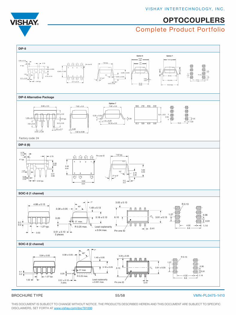
Complete Product Portfolio
THIS DOCUMENT IS SUBJECT TO CHANGE WITHOUT NOTICE. THE PRODUCTS DESCRIBED HEREIN AND THIS DOCUMENT ARE SUBJECT TO SPECIFIC DISCLAIMERS, SET FORTH AT www.vishay.com/doc?91000
VMN-PL0475-141055/58BROCHURE TyPE
OpTOCOupLErS
V I S H AY I N T E R T E C H N O LO GY, I N C .
DIp-8
DIp-8 Alternative package
DIp-8 (6)
SOIC-8 (1 channel)
SOIC-8 (2 channel)
0.26
3.5 ± 0.5
7.62 ± 0.3
0.5 ± 0.12.54 ± 0.25
3.3 ± 0.5
9.68 ± 0.5
7.62 to 9.98
0.5 typ.
2.8 ± 0.5
6.5 ± 0.5
7 6 5
1 2 3 4
8
1.25 ± 0.1 0.26
7.62 ± 0.3
10.16 ± 0.3
0.35 ± 0.25
Option 7
1.0 ± 0.25
2.541.50
1.3010.3
40°
7°
Pin one ID
5° max. 0.91
0.36
4.32 1.146.6
R 0.13
1.276.10
1.27 typ.0.41
0.10.2
Lead coplanarity± 0.04 max.
0.20
3.05 ± 0.13
CL
R 0.25 max.
0.53
3.91 ± 0.13
0.38 ± 0.05
4.88 ± 0.13
0.51 ± 0.102 places
1.49 ± 0.13
3.18 ± 0.13
Pin one ID
6.645 ± 0.165
9.77 ± 0.14
0.95 ± 0.19
4° typ.
2.54 typ.
0.51 ± 0.05
3.555 ± 0.255
0.70 ± 0.1910°
3° to 9°
7.62 typ.
0.25 ± 0.05
3.045 ± 0.255
6.095 ± 0.255
4 3 2 1
0.79
1.275 6 7 8
0.350.25
10.1610.92
7.87.4
10.369.96
Option 6
8 min.
7.62 typ.
4.64.1
8.4 min.
10.3 max.
0.7
Option 7
2.54 R 0.25
1.78
0.76
1.528 min.11.05
Pin one ID
6.486.81
9.639.91
0.761.14
4° typ.
2.54 typ.
10°
3° to 9°
7.62 typ.
0.460.56
0.20.3
2.793.30
3.303.81
0.510.89
5.846.35
4 3 2 1
0.79
1.275 6 8
0.91
0.36
4.32 1.146.6
R 0.13
1.27
40°
6.10
1.27 typ.
0.41
0.10.2
Lead coplanarity± 0.001 max.
0.20
7°
3.05 ± 0.05
CL
R 0.25 max.
1.02
5° max.
Pin one ID
3.91 ± 0.05
0.38 ± 0.055.84 ± 0.05
0.51 ± 0.102 plcs.
1.49 ± 0.05
3.18 ± 0.05
Factory code: 24
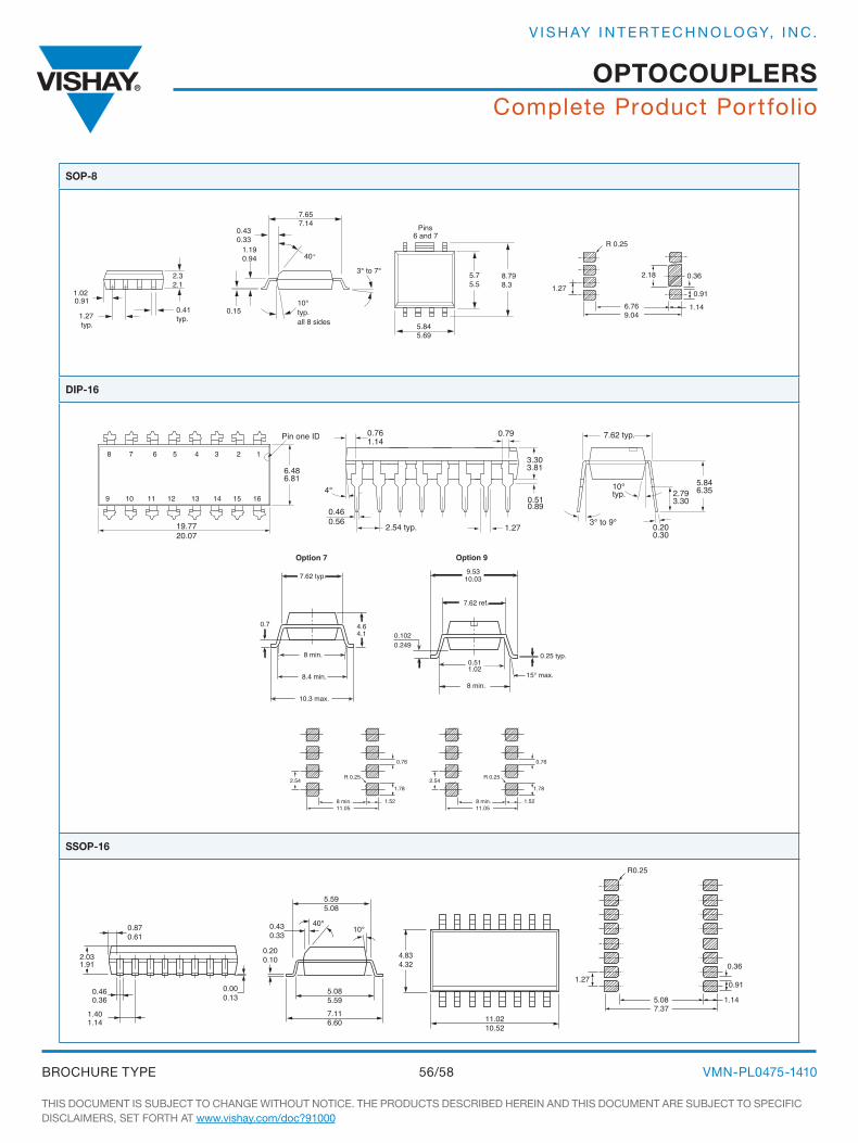
Complete Product Portfolio
THIS DOCUMENT IS SUBJECT TO CHANGE WITHOUT NOTICE. THE PRODUCTS DESCRIBED HEREIN AND THIS DOCUMENT ARE SUBJECT TO SPECIFIC DISCLAIMERS, SET FORTH AT www.vishay.com/doc?91000
VMN-PL0475-141056/58BROCHURE TyPE
OpTOCOupLErS
V I S H AY I N T E R T E C H N O LO GY, I N C .
1.020.91
40°
3° to 7°
10°typ.all 8 sides
Pins6 and 7
5.845.69
5.75.5
8.798.3
7.657.14
0.430.33
1.190.94
0.151.27 typ.
0.41typ.
2.32.1
R 0.25
1.27
2.18 0.36
1.146.769.04
0.91
6.486.81
19.7720.07
0.761.14
4°
2.54 typ.
10°typ.
3° to 9°0.460.56
0.200.30
2.793.30
Pin one ID
3.303.81
8 7 6 5 4 3 2 1
9 10 11 12 13 14 15 16
7.62 typ.
5.846.35
1.27
0.510.89
0.79
6.486.81
19.7720.07
0.761.14
4°
2.54 typ.
10°typ.
3° to 9°0.460.56
0.200.30
2.793.30
Pin one ID
3.303.81
8 7 6 5 4 3 2 1
9 10 11 12 13 14 15 16
7.62 typ.
5.846.35
1.27
0.510.89
0.79
8 min.
0.511.02
7.62 ref.
9.5310.03
0.25 typ.
0.1020.249
15° max.
Option 9
8 min.
7.62 typ.
4.64.1
8.4 min.
10.3 max.
0.7
Option 7
2.54 R 0.25
1.78
0.76
1.528 min.11.05
2.54 R 0.25
1.78
0.76
1.528 min.11.05
0.430.33
5.595.08
40°10°
0.200.10
7.116.60
5.085.59
4.834.32
11.0210.52
0.870.61
0.460.36
0.000.13
1.401.14
2.031.91
1.270.91
0.36
5.08 1.147.37
R0.25
SOp-8
DIp-16
SSOp-16

Complete Product Portfolio
THIS DOCUMENT IS SUBJECT TO CHANGE WITHOUT NOTICE. THE PRODUCTS DESCRIBED HEREIN AND THIS DOCUMENT ARE SUBJECT TO SPECIFIC DISCLAIMERS, SET FORTH AT www.vishay.com/doc?91000
VMN-PL0475-141057/58BROCHURE TyPE
OpTOCOupLErS
V I S H AY I N T E R T E C H N O LO GY, I N C .
reference product Literature
• 4 Pin optocouplers with low input current product sheet www.vishay.com/doc?49168
• Optical isolation for solar power applications guide www.vishay.com/doc?49185
• Phototriac selector guide www.vishay.com/doc?49828
• High-speed SSRs selector guide www.vishay.com/doc?49444
• Solid state relays (SSR) selector guide www.vishay.com/doc?49538
• Photovoltaic MOSFET driver with integrated fast turn-off selector guide www.vishay.com/doc?49261
• Photovoltaic single-component/isolated MOSFET driver solutions guide www.vishay.com/doc?49262
Complete Product Portfolio
THIS DOCUMENT IS SUBJECT TO CHANGE WITHOUT NOTICE. THE PRODUCTS DESCRIBED HEREIN AND THIS DOCUMENT ARE SUBJECT TO SPECIFIC DISCLAIMERS, SET FORTH AT www.vishay.com/doc?91000
VMN-PL0475-141058/58BROCHURE TyPE
OpTOCOupLErS
V I S H AY I N T E R T E C H N O LO GY, I N C .
THE AMErICAS
uNITED STATESVISHAy AMERICAS ONE GREENWICH PLACE SHELTON, CT 06484 UNITED STATES PH: +1-402-563-6866 FAX: +1-402-563-6296
ASIA
SINGApOrEVISHAy INTERTECHNOLOGy ASIA PTE LTD.37A TAMPINES STREET 92 #07-00SINGAPORE 528886 PH: +65-6788-6668 FAX: +65-6788-0988
p.r. CHINAVISHAy CHINA CO., LTD.15D, SUN TONG INFOPORT PLAZA55 HUAI HAI WEST ROADSHANGHAI 200030 P.R. CHINAPH: +86-21-22315555FAX: +86-21-22315551
JApANVISHAy JAPAN CO., LTD.SHIBUyA PRESTIGE BLDG. 4F 3-12-22, SHIBUyA SHIBUyA-KU TOKyO 150-0002 JAPAN PH: +81-3-5466-7150 FAX: +81-3-5466-7160
EurOpE
GErMANYVISHAy ELECTRONIC GMBHDR.-FELIX-ZANDMAN-PLATZ 1 95100 SELB GERMANy PH: +49-9287-71-0 FAX: +49-9287-70435 FrANCEVISHAy S.A.199, BD DE LA MADELEINE 06003 NICE, CEDEX 1 FRANCE PH: +33-4-9337-2727 FAX: +33-4-9337-2726 uNITED KINGDOMVISHAy LTD.SUITE 6C, TOWER HOUSEST. CATHERINE’S COURTSUNDERLAND ENTERPRISE PARKSUNDERLAND SR5 3XJ UNITED KINGDOMPH: +44-191-516-8584FAX: +44-191-549-9556
WORLDWIDE SALES CONTACTS
Recommended