Isha Padhy, Department of CSE, CBIT, Hyderabad
1
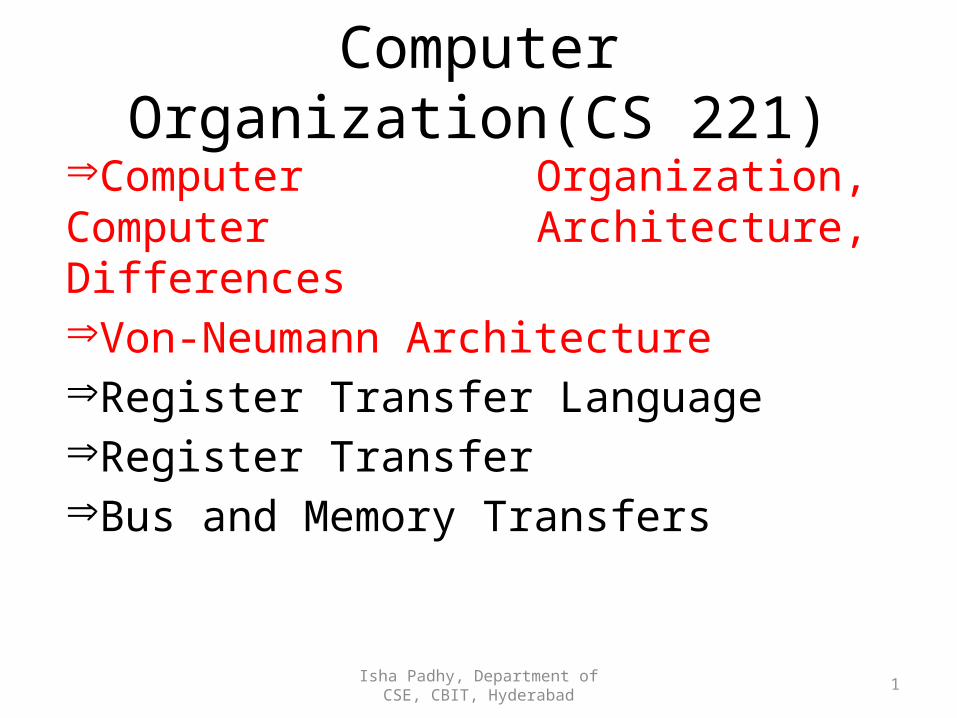
Computer Organization(CS 221)ÞComputer Organization, Computer Architecture, DifferencesÞVon-Neumann ArchitectureÞRegister Transfer LanguageÞRegister TransferÞBus and Memory Transfers
Isha Padhy, Department of CSE, CBIT, Hyderabad
2
• What is a computer?- A computer is a genera lpurpose programmable
electronic machine, having 2 principal characteristics:1. Responds to a specific set of coded instructions in
a well defined manner.2. It can execute a list of instructions termed as
program.• What is the difference between computers in starting
days and now?
Isha Padhy, Department of CSE, CBIT, Hyderabad
3
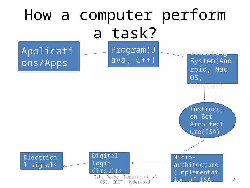
How a computer perform a task?
Instruction Set Architecture(ISA)
Applications/Apps
Program(Java, C++) Operating
System(Android, Mac OS, Windows)
Micro- architecture(Implementation of ISA)
Digital Logic Circuits
Electrical signals
Isha Padhy, Department of CSE, CBIT, Hyderabad
4
Computer organization and architecture
• Architecture describes what the computer does and organization describes how it does it.
• A computer's architecture is its abstract model and is the programmer's view in terms of instructions, addressing modes and registers. A computer's organisation expresses the realization of the architecture.
• Architecture and organisation are independent; you can change the organisation of a computer without changing its architecture.
Computer organization• Describes the function and the way computer components are operated and
the way they are connected together to form the computer system.Computer architecture - the structure and behavior of computer as seen by the user. - instruction formats, the instruction set and techniques for addressing memory.

Isha Padhy, Department of CSE, CBIT, Hyderabad
5
Some questions…
• Why has the speed of computer performance increased so much since 1970?
• Is the gear lever in a car part of its architecture or organization?
• Can u change the organization without changing the architecture?
Isha Padhy, Department of CSE, CBIT, Hyderabad
6
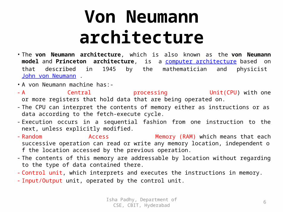
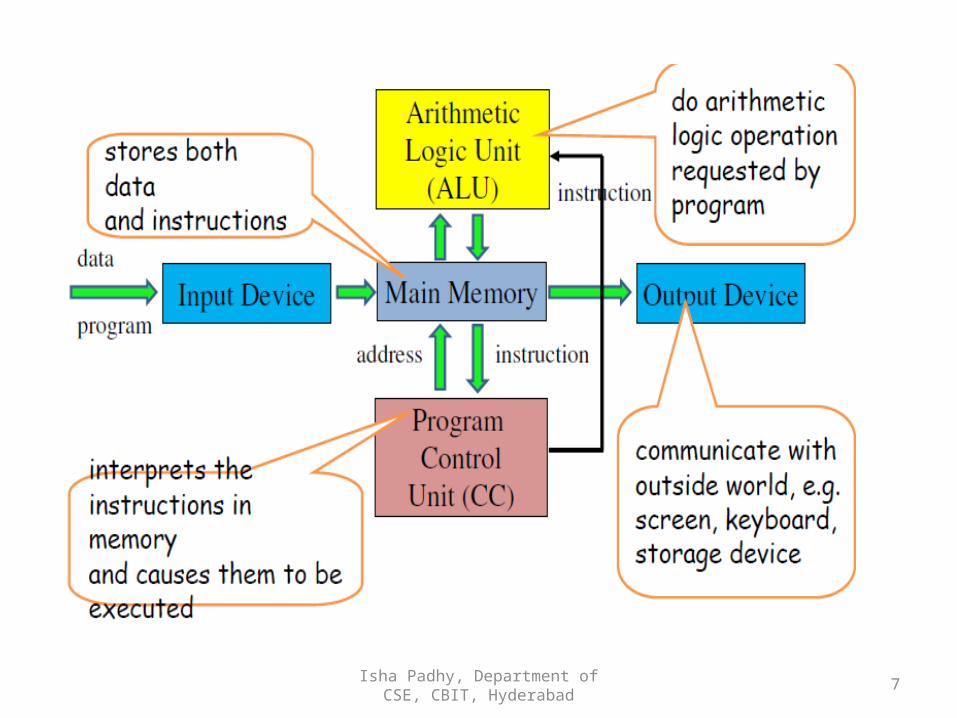
Von Neumann architecture• The von Neumann architecture, which is also known as the von Neumann model and Princeton
architecture, is a computer architecture based on that described in 1945 by the mathematician and physicist John von Neumann .
• A von Neumann machine has:-- A Central processing Unit(CPU) with one
or more registers that hold data that are being operated on.- The CPU can interpret the contents of memory either as instructions or as
data according to the fetch-execute cycle.- Execution occurs in a sequential fashion from one instruction to the next, unless explicitly
modified.- Random Access Memory (RAM) which means that each
successive operation can read or write any memory location, independent of the location accessed by the previous operation.
- The contents of this memory are addressable by location without regarding to the type of data contained there.
- Control unit, which interprets and executes the instructions in memory.- Input/Output unit, operated by the control unit.
Isha Padhy, Department of CSE, CBIT, Hyderabad
7
Isha Padhy, Department of CSE, CBIT, Hyderabad
8
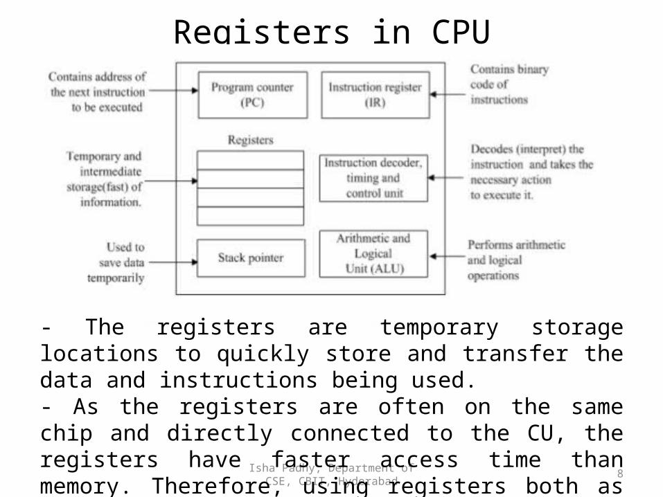
Registers in CPU
- The registers are temporary storage locations to quickly store and transfer the data and instructions being used. - As the registers are often on the same chip and directly connected to the CU, the registers have faster access time than memory. Therefore, using registers both as the source of operands and as the destination of results will improve the performance.
Isha Padhy, Department of CSE, CBIT, Hyderabad
9
Memory unit• The function of the memory is to store programs and data.• There are two classes of storage, called primary and secondary.- Primary storage is a fast memory that operates at electronic speeds. Programs must stay in memory while they are being executed. The memory contains a large number of semiconductor storage cells, each
capable of storing one bit of information.Random access memory: Memory in which any location can be reached in a
short and fixed amount of time after specifying its address is called random access memory (RAM).
- Secondary storage:• Although primary storage is essential, it tends to be expensive.• Thus additional, cheaper, secondary storage is used when large amounts of
data and many programs have to be stored, particularly for information that is accessed infrequently.
• A wide selection of secondary storage devices is available, including magnetic disks,tapes and optical disks (CD-ROMs)
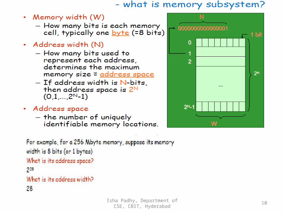
Isha Padhy, Department of CSE, CBIT, Hyderabad
10
Isha Padhy, Department of CSE, CBIT, Hyderabad
11
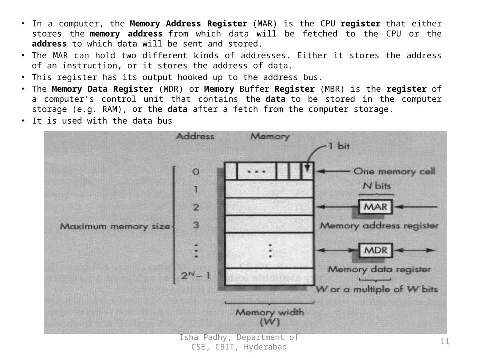
• In a computer, the Memory Address Register (MAR) is the CPU register that either stores the memory address from which data will be fetched to the CPU or the address to which data will be sent and stored.
• The MAR can hold two different kinds of addresses. Either it stores the address of an instruction, or it stores the address of data.
• This register has its output hooked up to the address bus.• The Memory Data Register (MDR) or Memory Buffer Register (MBR) is the register of a computer's
control unit that contains the data to be stored in the computer storage (e.g. RAM), or the data after a fetch from the computer storage.
• It is used with the data bus
12
Arithmetic and logic unit (ALU)• Most computer operations are executed in the arithmetic
and logic unit (ALU) of the processor.• Performs arithmetic operations(+,-,/,*) and logical
operations(AND,OR,NOT)
• For example, Suppose two numbers are to be added. • They are brought into the processor, and the actual addition
is carried out by the ALU.
• The sum may then be stored in the memory or retained in the processor for immediate use.
• When operands are brought into the processor, they are stored in high-speed storage elements called registers.
Isha Padhy, Department of CSE, CBIT, Hyderabad
Isha Padhy, Department of CSE, CBIT, Hyderabad
Control Unit
- Control unit determines the order in which instructions should be executed and controls the retrieval of the proper operands.- It interprets the instructions of the machine.
Isha Padhy, Department of CSE, CBIT, Hyderabad
14
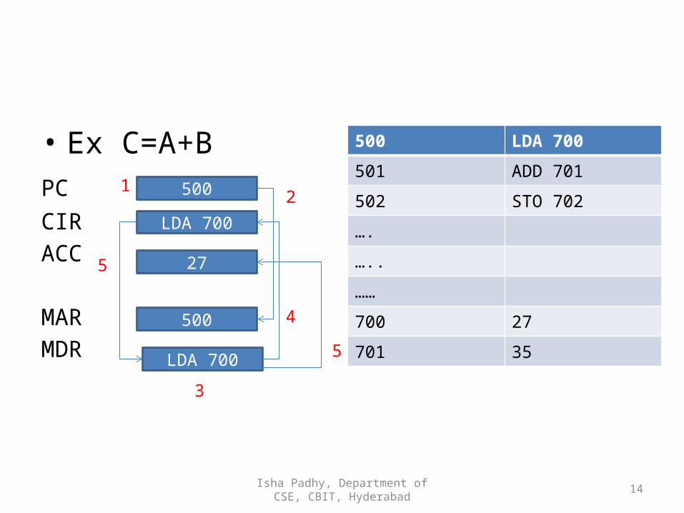
• Ex C=A+BPC CIRACC
MARMDR
500 LDA 700501 ADD 701502 STO 702….…..……700 27701 35
500
LDA 700
27
500
LDA 700
12
3
4
5
5
Isha Padhy, Department of CSE, CBIT, Hyderabad
15
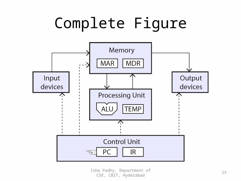
Complete Figure
Isha Padhy, Department of CSE, CBIT, Hyderabad
16
Register Transfer Language• The hardware organization of a digital computer is defined by specifying: The set of register it contains and their function. The sequence of micro- operations performed on the binary information stored in the
registers. The control that initiates the sequence of micro-operations
• A computer system is made of different digital modules which are designed using registers, decoders, control logics.
• Every module has a set of registers and some operations are done on data in these registers.
• RTL is the symbolic notation used to describe the micro-operation transfers among registers.
- Micro-operations are elementary operations performed on the information stored in one or more registers.
- An instruction is fetched from memory, decoded and executed by performing a sequence of micro-operations.
- The micro-operations only specify which data transfers may occur , they don’t specify when or how they may occur.
Isha Padhy, Department of CSE, CBIT, Hyderabad
17
Register Transfer• Registers are denoted by capital letters and are sometimes followed by
numerals• Register are notated by a name of choice. Ex A, R3 or pre-described names
like PC, MAR.• The most sig. bit of an n-bit register is bit n-1; the least sig. is bit 0.• Copying all the contents of one register to another is a register transfer.- Indicated as R2<-R11. In this case the contents of register R1 are copied (loaded) into register
R2.2. A simultaneous transfer of all bits from the source R1 to the destination
R2, during one clock pulse.3. The digital system has the data lines from the source register(R1)to (R2). 4. We can save a specific number to a register.5. Note: the contents of R1 are not altered.6. We cannot transfer information from r1->r1.7. All RTL instruction take one clock cycle to complete.
Isha Padhy, Department of CSE, CBIT, Hyderabad
18
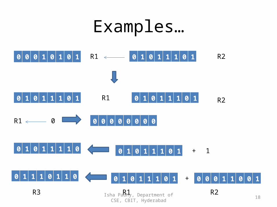
Examples…0 0 0 1 0 1 0 1 R1 0 1 0 1 1 1 0 1 R2
R2R1 0 1 0 1 1 1 0 10 1 0 1 1 1 0 1
R1 0 0 0 0 0 0 0 0 0
0 1 0 1 1 1 0 1 0 0 0 1 1 0 0 10 1 1 1 0 1 1 0 +
R1 R2R3
0 1 0 1 1 1 1 0 0 1 0 1 1 1 0 1 1+
Isha Padhy, Department of CSE, CBIT, Hyderabad
19
Isha Padhy, Department of CSE, CBIT, Hyderabad
20
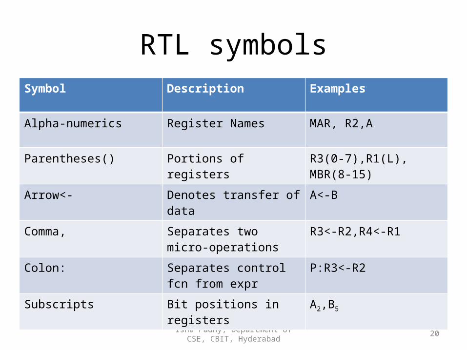
RTL symbolsSymbol Description Examples
Alpha-numerics Register Names MAR, R2,A
Parentheses() Portions of registers R3(0-7),R1(L), MBR(8-15)
Arrow<- Denotes transfer of data A<-B
Comma, Separates two micro-operations
R3<-R2,R4<-R1
Colon: Separates control fcn from expr
P:R3<-R2
Subscripts Bit positions in registers A2,B5
Control Functions
Isha Padhy, Department of CSE, CBIT, Hyderabad 21
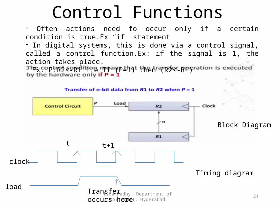
- Often actions need to occur only if a certain condition is true.Ex “if” statement- In digital systems, this is done via a control signal, called a control function.Ex: if the signal is 1, the action takes place.- Ex. P:R2<-R1 i.e If (P=1) then (R2<-R1)
clock
load
t t+1
Transfer occurs here
Timing diagram
Block Diagram
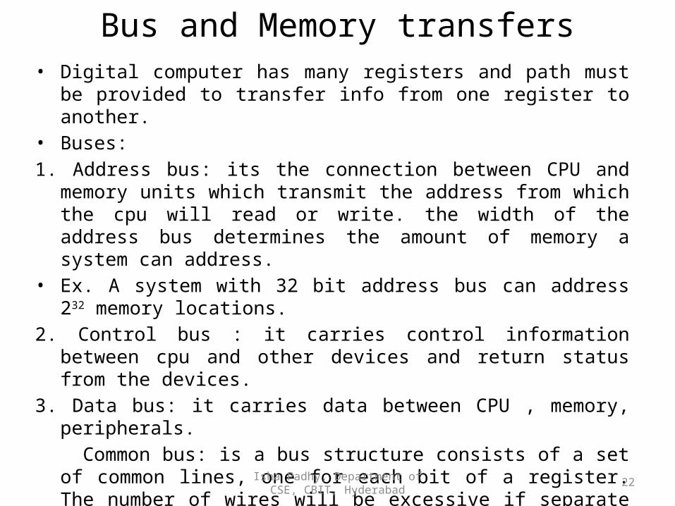
Bus and Memory transfers• Digital computer has many registers and path must be provided to transfer
info from one register to another.• Buses:1. Address bus: its the connection between CPU and memory units which
transmit the address from which the cpu will read or write. the width of the address bus determines the amount of memory a system can address.
• Ex. A system with 32 bit address bus can address 232 memory locations.2. Control bus : it carries control information between cpu and other devices
and return status from the devices.3. Data bus: it carries data between CPU , memory, peripherals. Common bus: is a bus structure consists of a set of common lines, one for
each bit of a register. The number of wires will be excessive if separate lines are used between each register to all other register.
• Control signals determine which register is connected with a bus line.• When a bus is included in the statement, the register transfer is given as
BUS<- C, R1<- BUS So we can say R1<- C i.e C contents are transferred to R1 by activating its load control input.
Isha Padhy, Department of CSE, CBIT,
Hyderabad 22
Isha Padhy, Department of CSE, CBIT, Hyderabad
23
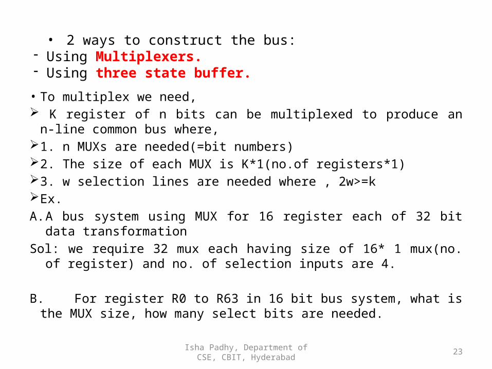
• To multiplex we need, K register of n bits can be multiplexed to produce an n-line common bus
where, 1. n MUXs are needed(=bit numbers) 2. The size of each MUX is K*1(no.of registers*1) 3. w selection lines are needed where , 2w>=k Ex.A. A bus system using MUX for 16 register each of 32 bit data transformationSol: we require 32 mux each having size of 16* 1 mux(no. of register) and no.
of selection inputs are 4.
B. For register R0 to R63 in 16 bit bus system, what is the MUX size, how many select bits are needed.
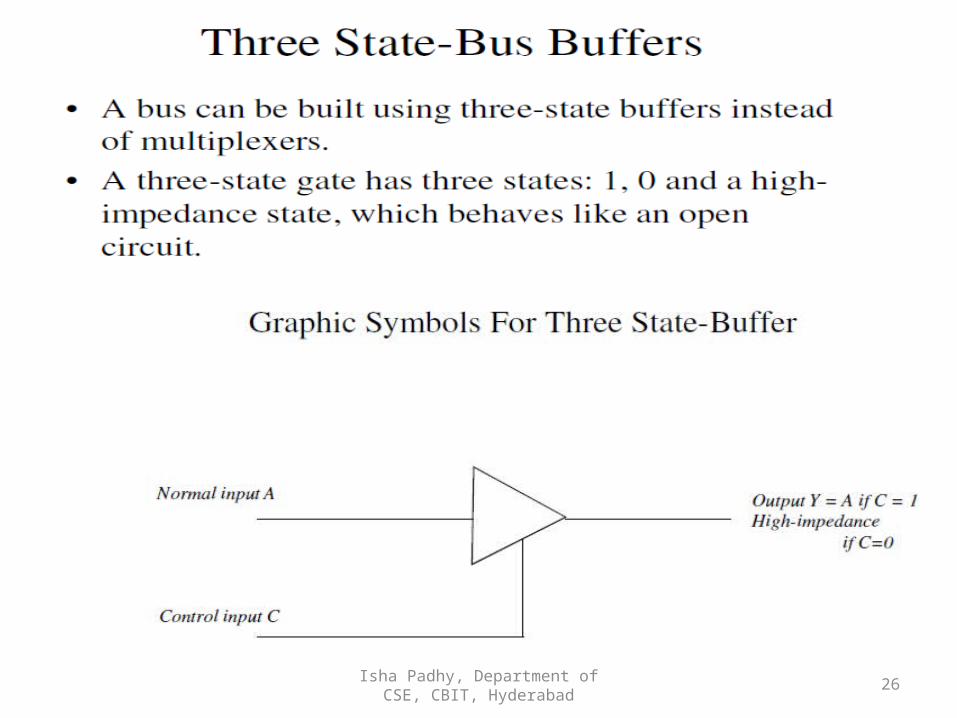
• 2 ways to construct the bus:- Using Multiplexers.- Using three state buffer.
Isha Padhy, Department of CSE, CBIT, Hyderabad
24
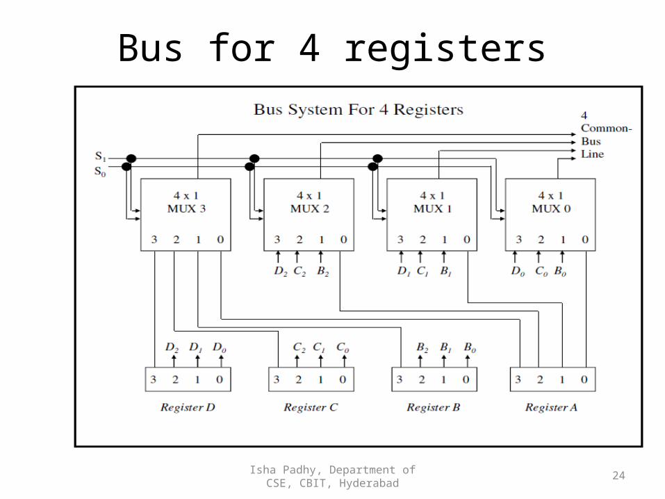
Bus for 4 registers

Isha Padhy, Department of CSE, CBIT, Hyderabad
25
• We get n=4,k=4 so here we use 4 mux each having 4*1 size.
• As each mux is 4*1 , each mux have 2 selection inputs in the bus. We denote by S0, S1 . This selection select the 1 line output from 0 to 3 available in each mux and applied to the o/p that form a bus system.
• Here each register have 4 positive triggered flip-flop set.
When S1S0=00, the 0 data inputs of all 4 mux are selected and applied to the ouputs that form the bus.This causes the bus lines to receive the content of reg A since the outputs of this register are connected to the 0 data inputs of the mux.
Isha Padhy, Department of CSE, CBIT, Hyderabad
26
Isha Padhy, Department of CSE, CBIT, Hyderabad
27
- Enable input=0,all 4 o/ps are 0, bus line= high- impedance state.- Enable input is active, depending the value of S0, S1, one of the output decoder is active, so one of the 3 state buffer i/p is active
Memory transfer
- The transfer of info from a memory word to the outside envoirenment is called a read operation.
- The transfer of new info to be stored into the memory is called a write operation.
- The read operation can be stated as,DR <- M[AR]DR=Data register(Memory transfers data to this register)AR= Address register(Memory gets the address from this register)This causes a transfer of info into DR from the memory word M selected by the address in AR.
- The write operation transfers the content of a data register to a memory word M selected by the address.M[AR]<- R1
Isha Padhy, Department of CSE, CBIT, Hyderabad 28
Isha Padhy, Department of CSE, CBIT, Hyderabad
29
Micro-operations• A micro-operation is an operation performed with the data stored in
registers.• 4 types:-1. Register transfer micro-operations: transfer binary information from
one register to another.2. Arithmetic micro-operations: perform arithmetic operations on
numeric data stored in registers.3. Logic micro-operations: perform bit manipulation operations on
non- numeric data stored in registers.4. Shift micro-operations perform shift operations on data stored in
registers.• In all operations except first one the contents of the register changes.
Isha Padhy, Department of CSE, CBIT, Hyderabad
30
Arithmetic micro-operation• -Addition (R3<- R1+ R2: contents of register R1, R2 are
summed up and stored in R3A <- Ā +1: 2’s complement of A)
• Subtraction (R3<- R1 – A: contents of R1 minus A, transferred to R3.Or R3<- R1+ Ā +1 : 1’s complement of A + 1=2’s compl)
• Increment (R1<- R1+1, increment the content by 1)• Decrement (R1<-R1 – 1, decrement the content by 1)• A micro-operation is one that can be executed by one clock
pulse . Multiply (divide) is implemented by a sequence of add and shift micro-operations (subtract and shift)
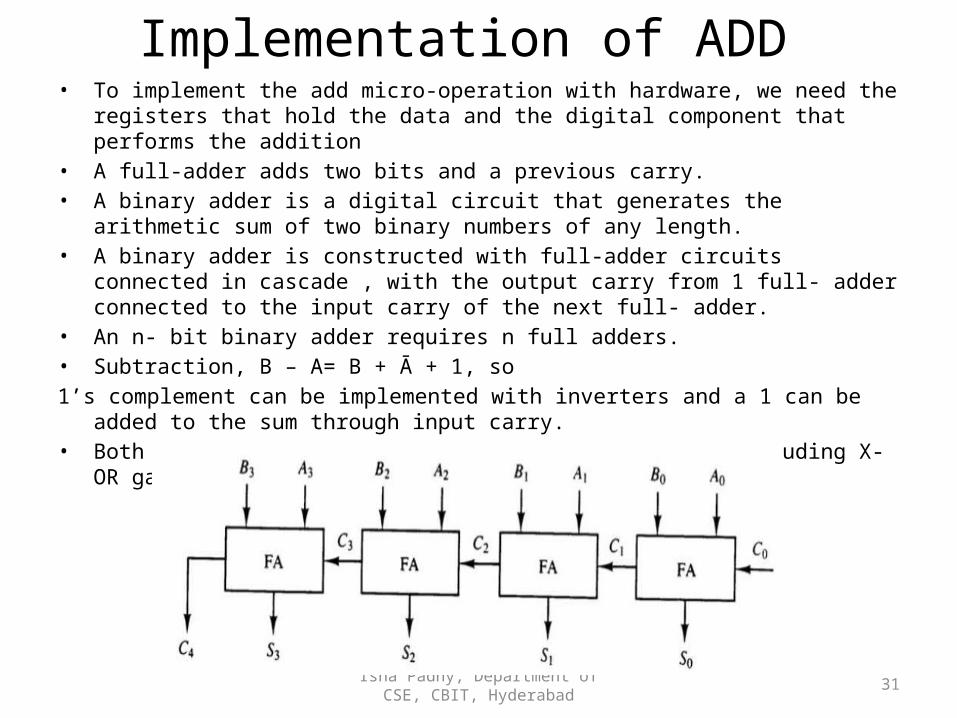
Implementation of ADD • To implement the add micro-operation with hardware, we need the registers that hold the data
and the digital component that performs the addition • A full-adder adds two bits and a previous carry.• A binary adder is a digital circuit that generates the arithmetic sum of two binary numbers of
any length.• A binary adder is constructed with full-adder circuits connected in cascade , with the output
carry from 1 full- adder connected to the input carry of the next full- adder.• An n- bit binary adder requires n full adders. • Subtraction, B – A= B + Ā + 1, so1’s complement can be implemented with inverters and a 1 can be added to the sum through input
carry.• Both add and subtract can be combined into one by including X-OR gate with each full adder.
Isha Padhy, Department of CSE, CBIT, Hyderabad 31
Isha Padhy, Department of CSE, CBIT, Hyderabad
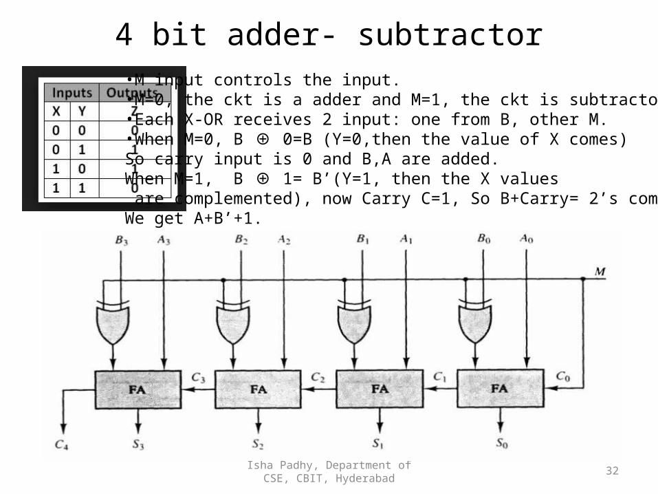
32
4 bit adder- subtractor•M input controls the input.•M=0, the ckt is a adder and M=1, the ckt is subtractor.•Each X-OR receives 2 input: one from B, other M.•When M=0, B 0=B (Y=0,then the value of X comes)⊕So carry input is 0 and B,A are added.When M=1, B 1= B’(Y=1, then the X values⊕ are complemented), now Carry C=1, So B+Carry= 2’s complement.We get A+B’+1.
Isha Padhy, Department of CSE, CBIT, Hyderabad
33
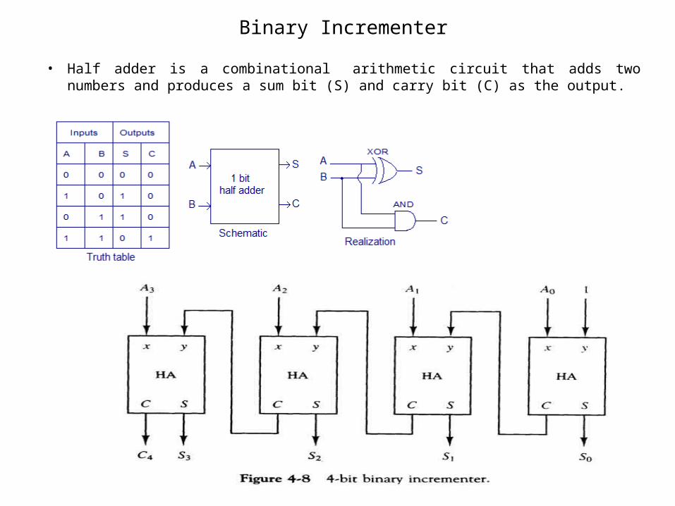
Binary Incrementer
• Half adder is a combinational arithmetic circuit that adds two numbers and produces a sum bit (S) and carry bit (C) as the output.
Isha Padhy, Department of CSE, CBIT, Hyderabad
34
Logic micro-operations
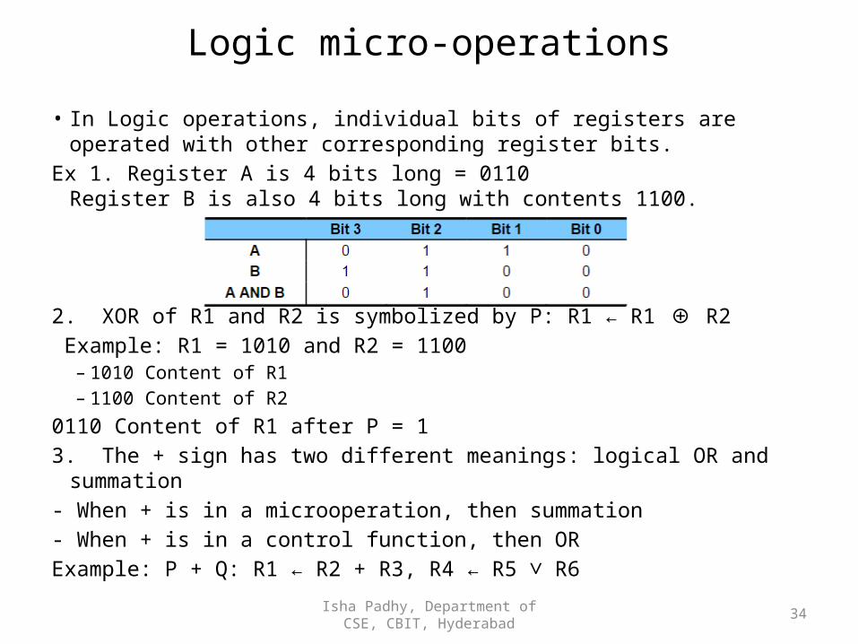
• In Logic operations, individual bits of registers are operated with other corresponding register bits.
Ex 1. Register A is 4 bits long = 0110Register B is also 4 bits long with contents 1100.
2. XOR of R1 and R2 is symbolized by P: R1 ← R1 R2 ⊕ Example: R1 = 1010 and R2 = 1100
– 1010 Content of R1 – 1100 Content of R2
0110 Content of R1 after P = 13. The + sign has two different meanings: logical OR and summation - When + is in a microoperation, then summation - When + is in a control function, then OR Example: P + Q: R1 ← R2 + R3, R4 ← R5 R6 ∨
Isha Padhy, Department of CSE, CBIT, Hyderabad
35
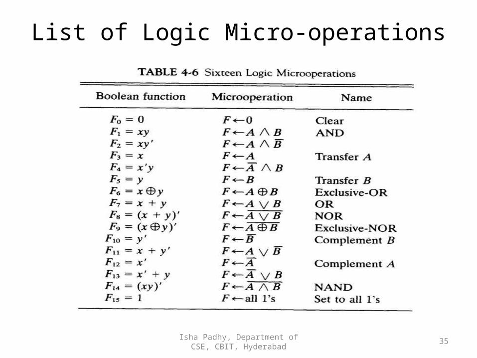
List of Logic Micro-operations
Isha Padhy, Department of CSE, CBIT, Hyderabad
36
• The hardware implementation of logic micro-operations requires that logic gates be inserted for each bit or pair of bits in the registers
• All 16 micro-operations can be derived from using four logic gates AND, OR, XOR, complement.
Isha Padhy, Department of CSE, CBIT, Hyderabad
37
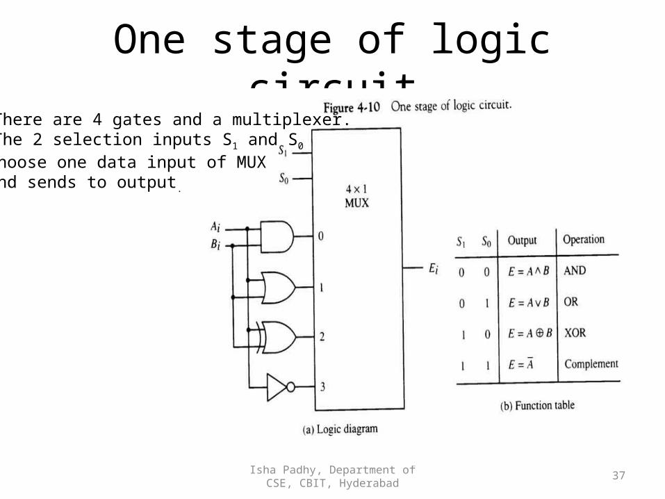
One stage of logic circuit-There are 4 gates and a multiplexer.-The 2 selection inputs S1 and S0
choose one data input of MUX and sends to output.
Isha Padhy, Department of CSE, CBIT, Hyderabad
38
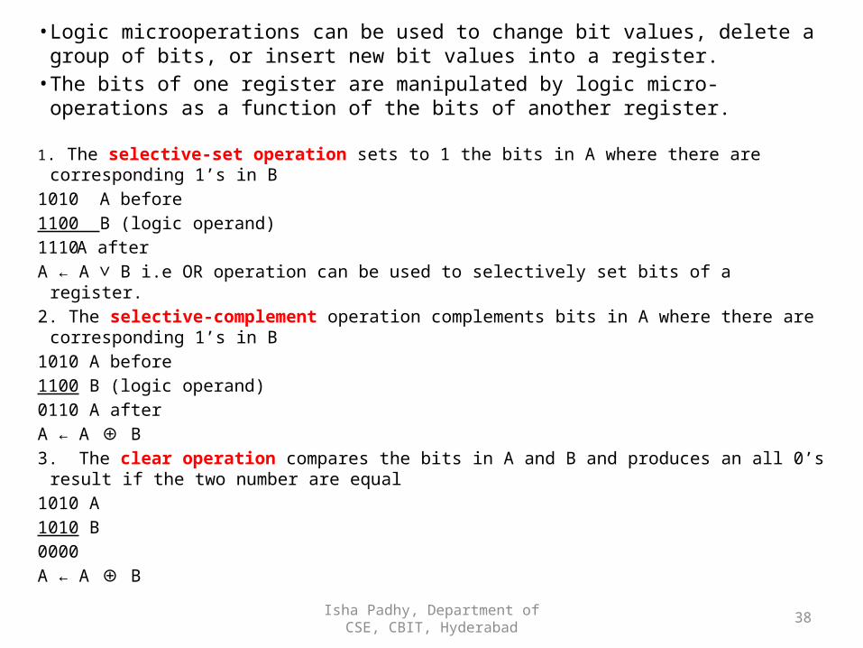
• Logic microoperations can be used to change bit values, delete a group of bits, or insert new bit values into a register.
• The bits of one register are manipulated by logic micro-operations as a function of the bits of another register.
1. The selective-set operation sets to 1 the bits in A where there are corresponding 1’s in B 1010 A before 1100 B (logic operand) 1110 A after A ← A B i.e OR operation can be used to selectively set bits of a register.∨2. The selective-complement operation complements bits in A where there are corresponding 1’s in B 1010 A before 1100 B (logic operand) 0110 A after A ← A B ⊕3. The clear operation compares the bits in A and B and produces an all 0’s result if the two number
are equal 1010 A 1010 B 0000A ← A B ⊕
Isha Padhy, Department of CSE, CBIT, Hyderabad
39
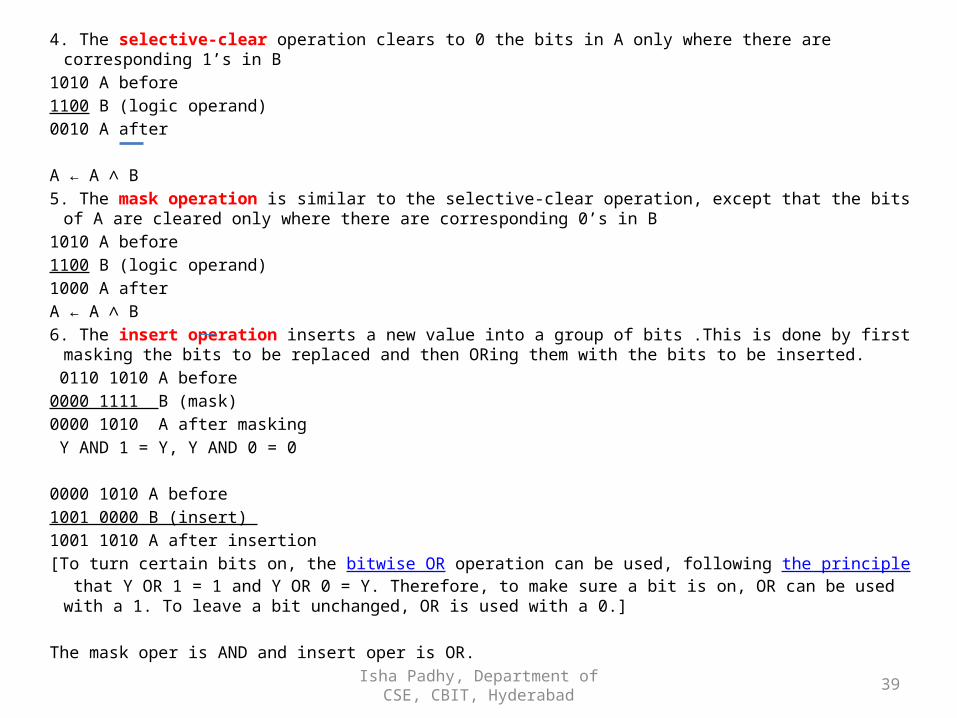
4. The selective-clear operation clears to 0 the bits in A only where there are corresponding 1’s in B 1010 A before 1100 B (logic operand) 0010 A after
A ← A B∧5. The mask operation is similar to the selective-clear operation, except that the bits of A are cleared only where there
are corresponding 0’s in B 1010 A before 1100 B (logic operand) 1000 A after A ← A B ∧6. The insert operation inserts a new value into a group of bits .This is done by first masking the bits to be replaced and
then ORing them with the bits to be inserted. 0110 1010 A before 0000 1111 B (mask)0000 1010 A after masking Y AND 1 = Y, Y AND 0 = 0
0000 1010 A before 1001 0000 B (insert) 1001 1010 A after insertion [To turn certain bits on, the bitwise OR operation can be used, following the principle that Y OR 1 = 1 and Y OR 0 = Y.
Therefore, to make sure a bit is on, OR can be used with a 1. To leave a bit unchanged, OR is used with a 0.]
The mask oper is AND and insert oper is OR.
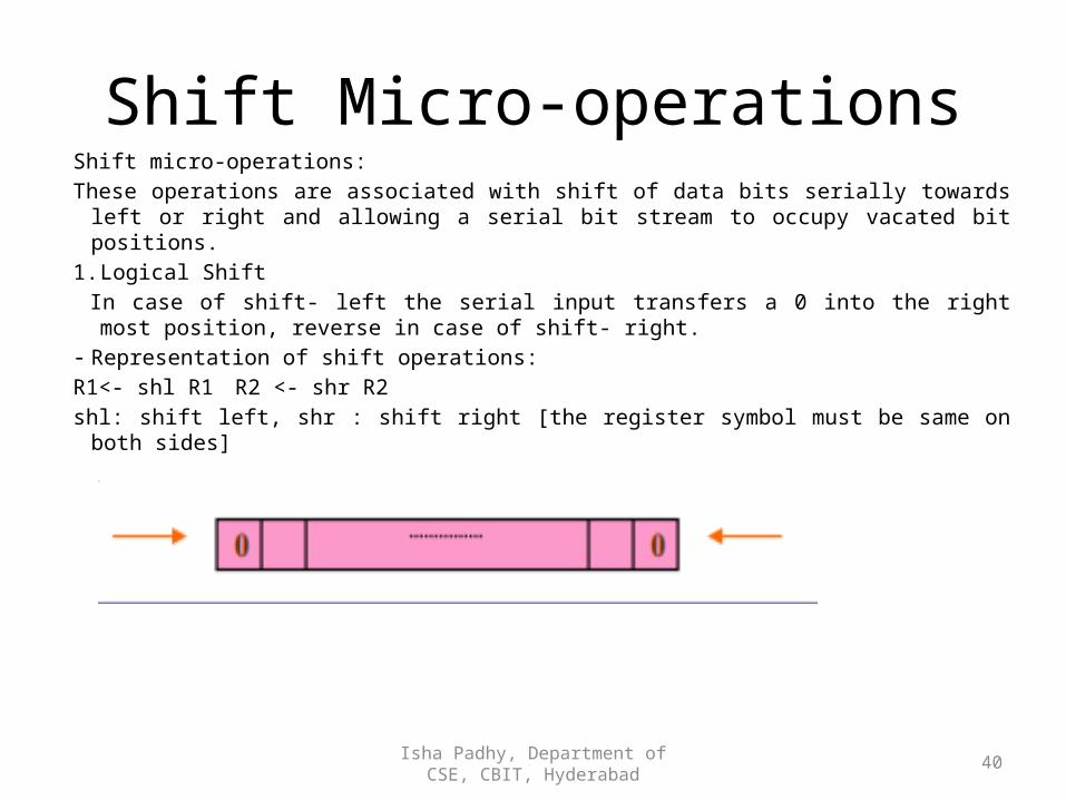
Shift Micro-operationsShift micro-operations: These operations are associated with shift of data bits serially towards left or right and
allowing a serial bit stream to occupy vacated bit positions. 1. Logical Shift In case of shift- left the serial input transfers a 0 into the right most position, reverse in
case of shift- right.- Representation of shift operations:R1<- shl R1 R2 <- shr R2shl: shift left, shr : shift right [the register symbol must be same on both sides]
Isha Padhy, Department of CSE, CBIT, Hyderabad 40
41Isha Padhy, Department of CSE, CBIT, Hyderabad
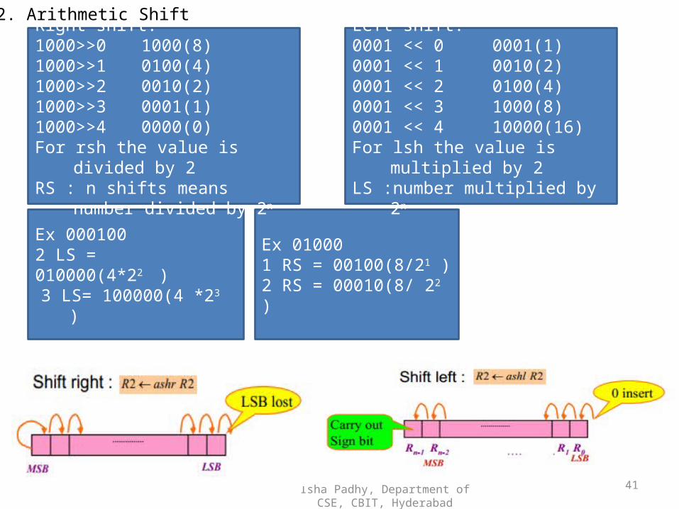
Ex 010001 RS = 00100(8/21 )2 RS = 00010(8/ 22 )
Ex 0001002 LS = 010000(4*22 ) 3 LS= 100000(4 *23 )
Right shift:1000>>0 1000(8)1000>>1 0100(4)1000>>2 0010(2)1000>>3 0001(1)1000>>4 0000(0)For rsh the value is divided by 2RS : n shifts means number divided
by 2n
Left shift:0001 << 0 0001(1)0001 << 1 0010(2)0001 << 2 0100(4)0001 << 3 1000(8)0001 << 4 10000(16)For lsh the value is multiplied by 2LS :number multiplied by 2n
2. Arithmetic Shift
Isha Padhy, Department of CSE, CBIT, Hyderabad 42
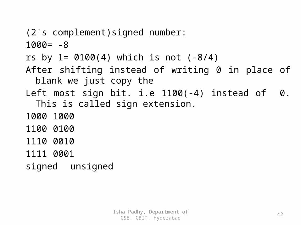
(2's complement)signed number:1000= -8rs by 1= 0100(4) which is not (-8/4)After shifting instead of writing 0 in place of blank we just copy theLeft most sign bit. i.e 1100(-4) instead of 0. This is called sign
extension.1000 10001100 01001110 00101111 0001signed unsigned
Isha Padhy, Department of CSE, CBIT, Hyderabad
43
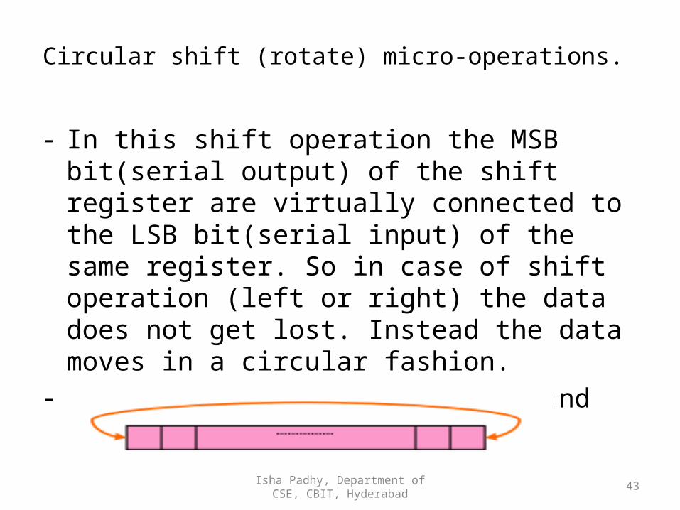
Circular shift (rotate) micro-operations.
- In this shift operation the MSB bit(serial output) of the shift register are virtually connected to the LSB bit(serial input) of the same register. So in case of shift operation (left or right) the data does not get lost. Instead the data moves in a circular fashion.
- Denoted as cil(circular left) and cir(circular right).
Isha Padhy, Department of CSE, CBIT, Hyderabad
44
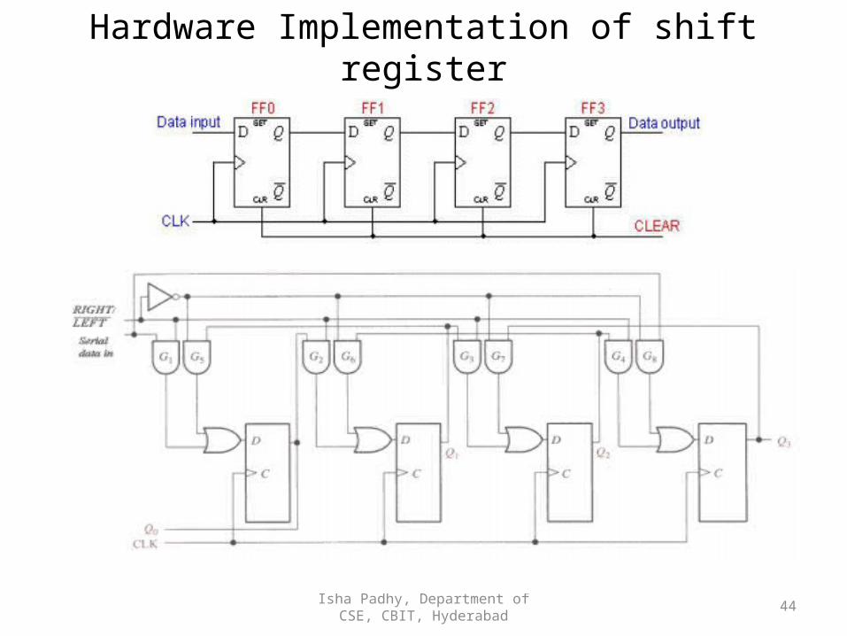
Hardware Implementation of shift register
Isha Padhy, Department of CSE, CBIT, Hyderabad
45
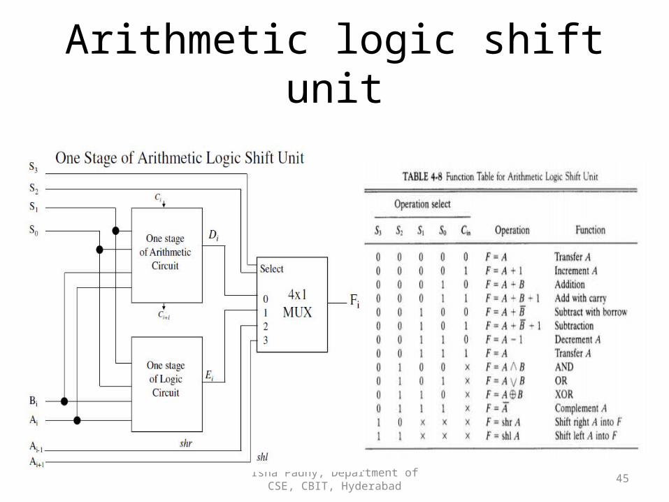
Arithmetic logic shift unit
Isha Padhy, Department of CSE, CBIT, Hyderabad
46
Description of ALU• To perform a micro-operation the contents of specified registers are placed in the inputs of the
common ALU.• The results are send to the concerned register.• ALU is a combinational circuit, where any register transfer operation is done in 1 clock pulse.• ALU consist of Arithmetic circuit, Logical circuit and Shift circuit. - Ai , Bi are inputs at any stage.- Inputs are given to both Arithmetic and logic unit.- S0,S1 selects particular micro-operation.- A 4*1 MUX selects output from arithmetic unit Ei or logic unit Hi.- Data in MUX is selected with S3,S2.- MUX receives other 2 inputs as Ai-1( shift right) and Ai+1(shift- left).- The CKT will be repeated n- times for n-bit operation.- The carry Ci+1 will be connected to Ci of next stage.- Cin is involved in selection process of arithmetic operations.- This provides 8 arithmetic operations(23[S0,S1,Ci]), 4 logic operations(22[S0,S1]), 2 shift
operations. So 14 operations are possible, first 8 arithmetic, next 4 logic and last 2 shift.
Isha Padhy, Department of CSE, CBIT, Hyderabad
47
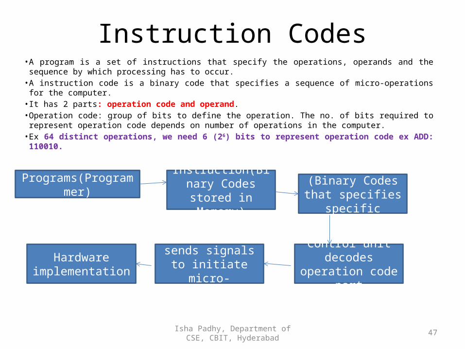
Instruction Codes• A program is a set of instructions that specify the operations, operands and the sequence by which
processing has to occur.• A instruction code is a binary code that specifies a sequence of micro-operations for the computer.• It has 2 parts: operation code and operand.• Operation code: group of bits to define the operation. The no. of bits required to represent
operation code depends on number of operations in the computer.• Ex 64 distinct operations, we need 6 (26) bits to represent operation code ex ADD: 110010.
Programs(Programmer)Instruction(Binary
Codes stored in Memory)
Control unit decodes operation code part
Operation (Binary Codes that specifies specific operation)
Control unit sends signals to initiate micro-operations
Hardware implementation
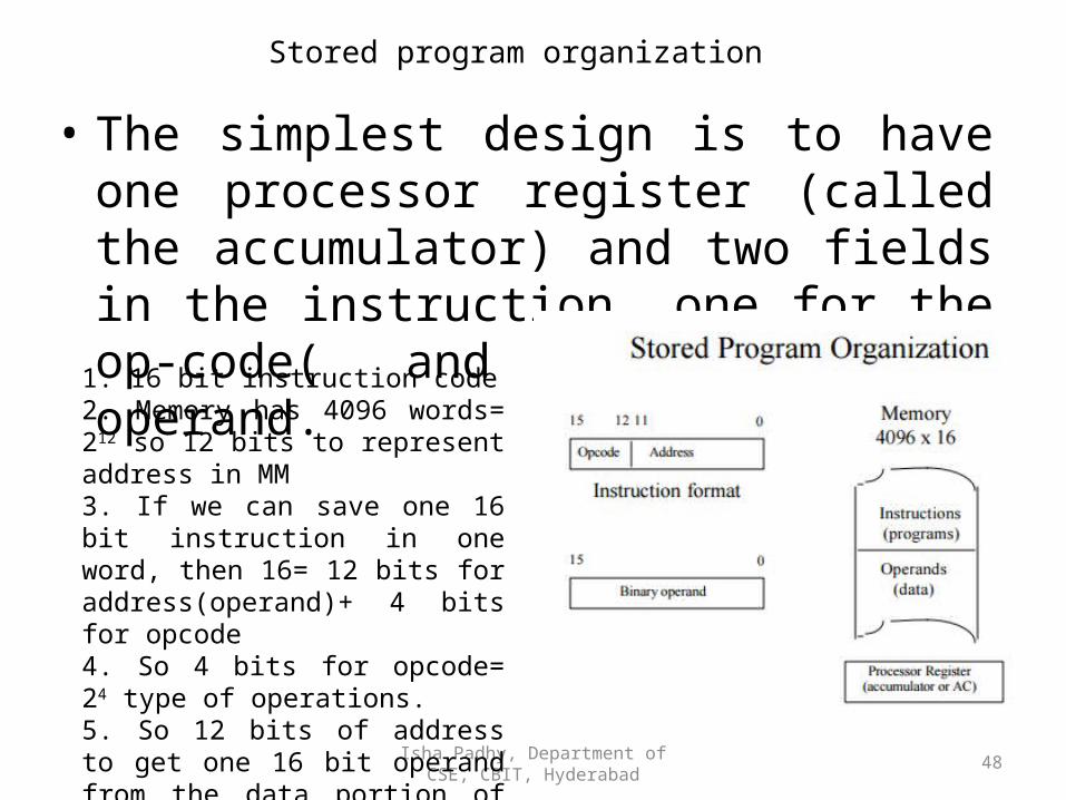
Stored program organization
• The simplest design is to have one processor register (called the accumulator) and two fields in the instruction, one for the op-code( and one for the operand.
Isha Padhy, Department of CSE, CBIT, Hyderabad 48
1. 16 bit instruction code2. Memory has 4096 words= 212 so 12 bits to represent address in MM3. If we can save one 16 bit instruction in one word, then 16= 12 bits for address(operand)+ 4 bits for opcode4. So 4 bits for opcode= 24 type of operations. 5. So 12 bits of address to get one 16 bit operand from the data portion of memory.
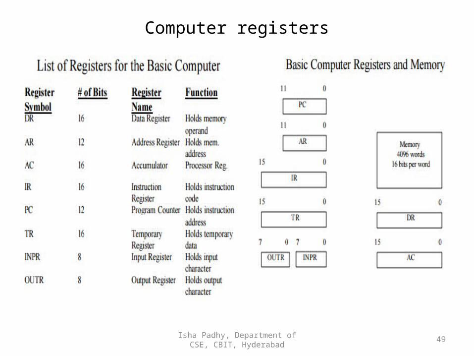
Computer registers
Isha Padhy, Department of CSE, CBIT, Hyderabad 49
Isha Padhy, Department of CSE, CBIT, Hyderabad
50
Isha Padhy, Department of CSE, CBIT, Hyderabad
51
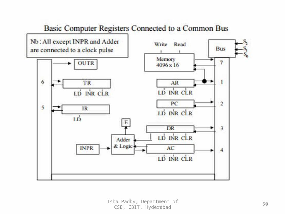
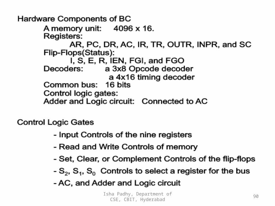
• The basic computer has 8 registers, memory unit, control unit.• 7 register and memory are selected based on S0S1S2.
- The decimal number at each output shows when the register can place the content onto the bus. Ex DR can put its content when S0S1S2=011.The register whose LD is active can receive input from bus. Memory receives the input when write input is enabled. The memory places its 16 bit output when read input is activated and S0S1S2=111.
- Size of DR,AC,IR,TR=16 whereas size of PC,AR= 12 bits. So when contents of AR, PC are placed on to bus the 4 MSB are set to 0. When they receive info from bus only 12 LSB bits are transferred into register. The size of INPR, OUTR have 8 bits and communicate with 8 LSB in the bus.
- INPR: provides info to bus(info from i/p device ,transfers to AC)OUTR: receives info from bus( receives a character from AC, transfers to o/p device).
- The input data and output data from and to 6 registers and memory are done with the bus. The memory address is connected to AR.(So no need of extra address bus required to transfer address). Any register can receive data from memory except AC.
- The 16 inputs of AC come from an adder and logic circuits. The CKT has 3 inputs. 1 set comes from the output of AC. They are used for implementation of register micro-operations s.a. complement AC, Shift AC. 1 set comes from DR. The inputs from DR, AC are used for Arithmetic and logic micro-operations s.a. ADD DR to AC. E holds the carry bit. 1 set comes from input register INPR.
- DR<-AC, AC<-DR can be done in 1 clock cycle.
Isha Padhy, Department of CSE, CBIT, Hyderabad
52
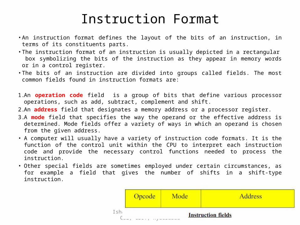
Instruction Format• An instruction format defines the layout of the bits of an instruction, in terms of its constituents
parts.• The instruction format of an instruction is usually depicted in a rectangular box symbolizing
the bits of the instruction as they appear in memory words or in a control register.• The bits of an instruction are divided into groups called fields. The most common fields found
in instruction formats are:
1. An operation code field is a group of bits that define various processor operations, such as add, subtract, complement and shift.
2. An address field that designates a memory address or a processor register.3. A mode field that specifies the way the operand or the effective address is determined. Mode
fields offer a variety of ways in which an operand is chosen from the given address.• A computer will usually have a variety of instruction code formats. It is the function of the
control unit within the CPU to interpret each instruction code and provide the necessary control functions needed to process the instruction.
• Other special fields are sometimes employed under certain circumstances, as for example a field that gives the number of shifts in a shift-type instruction.
Isha Padhy, Department of CSE, CBIT, Hyderabad
53
• Operations specified by computer instructions are executed on some data stored in memory or processor registers,
• Operands residing in processor registers are specified with a register address.
• A register address is a binary number of k bits that defines one of 2k registers in the CPU. Thus a CPU with 16 processor registers R0 through R15 will have a register address field of four bits. The binary number 0101, for example, will designate register R5.
• Computers may have instructions of several different lengths containing varying number of addresses. The number of address fields in the instruction format of a computer depends on the internal organization of its registers.
• Most computers fall into one of three types of CPU organizations: 1. Single accumulator organization. 2. General register organization. 3. Stack organization.
Isha Padhy, Department of CSE, CBIT, Hyderabad
54
CPU organizations1. Single accumulator organization. - All operations are performed with an implied accumulator register. - The instruction format in this type of computer uses one address field. - Ex ADD X //X is the address of the operand
AC ← AC + M[X]2. General register organization- The instruction format in this type of computer needs three register address fields.- ADD R1, R2, R3
To denote the operation R1 ← R2 + R3.- The number of address fields in the instruction can be reduced from three to two if the destination
register is the same as one of the source registers. Thus the instruction ADD R1, R2 Would denote the operation R1 ← R1 + R2.
- Computers with multiple processor registers use the move instruction with a mnemonic MOV to symbolize a transfer instruction. Thus the instruction MOV R1, R2 Denotes the transfer R1 ← R2 (or R2 ← R1, depending on the particular computer). Thus transfer-type instructions need two address fields to specify the source and the destination.
- Each address field may specify a processor register or a memory word. An instruction symbolized by ADD R1, X Would specify the operation R1 ← R + M [X]. It has two address fields, one for register R1 and the other for the memory address X.
3. Stack organization- Computers with stack organization would have PUSH and POP instructions which require an address
field. Thus the instruction PUSH X Will push the word at address X to the top of the stack. The stack pointer is updated automatically. Operation-type instructions do not need an address field in stack-organized computers. This is because the operation is performed on the two items that are on top of the stack. Ex ADD
Isha Padhy, Department of CSE, CBIT, Hyderabad
55
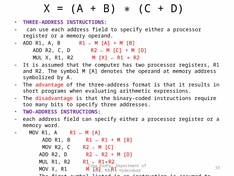
X = (A + B) (C + D) ∗• THREE-ADDRESS INSTRUCTIONS:- can use each address field to specify either a processor register or a memory operand.- ADD R1, A, B R1 ← M [A] + M [B] ADD R2, C, D R2 ← M [C] + M [D] MUL X, R1, R2 M [X] ← R1 R2 ∗- It is assumed that the computer has two processor registers, R1 and R2. The symbol M [A]
denotes the operand at memory address symbolized by A.- The advantage of the three-address format is that it results in short programs when evaluating
arithmetic expressions. - The disadvantage is that the binary-coded instructions require too many bits to specify three
addresses.• TWO-ADDRESS INSTRUCTIONS:- each address field can specify either a processor register or a memory word.- MOV R1, A R1 ← M [A] ADD R1, B R1 ← R1 + M [B] MOV R2, C R2 ← M [C] ADD R2, D R2 ← R2 + M [D] MUL R1, R2 R1 ← R1 R2∗ MOV X, R1 M [X] ← R1- The first symbol listed in an instruction is assumed to be both a source and the destination
where the result of the operation is transferred.
Isha Padhy, Department of CSE, CBIT, Hyderabad
56
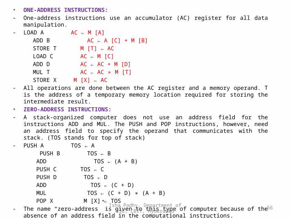
• ONE-ADDRESS INSTRUCTIONS: - One-address instructions use an accumulator (AC) register for all data manipulation. - LOAD A AC ← M [A] ADD B AC ← A [C] + M [B] STORE T M [T] ← AC LOAD C AC ← M [C] ADD D AC ← AC + M [D] MUL T AC ← AC M [T] ∗ STORE X M [X] ← AC- All operations are done between the AC register and a memory operand. T is the address of a temporary
memory location required for storing the intermediate result.• ZERO-ADDRESS INSTRUCTIONS: - A stack-organized computer does not use an address field for the instructions ADD and MUL. The PUSH
and POP instructions, however, need an address field to specify the operand that communicates with the stack. (TOS stands for top of stack)
- PUSH A TOS ← A PUSH B TOS ← B ADD TOS ← (A + B) PUSH C TOS ← C PUSH D TOS ← D ADD TOS ← (C + D) MUL TOS ← (C + D) (A + B) ∗ POP X M [X] ← TOS- The name “zero-address” is given to this type of computer because of the absence of an address field in the
computational instructions.
Isha Padhy, Department of CSE, CBIT, Hyderabad
57
Addressing Modes• The different ways in which a processor can
access data are called addressing modes. The operand can be present in a register, memory location.
• Operands to an instruction:- Source: input value to instruction- Destination: where result has to go.• Separate addressing mode for memory and
register.
Isha Padhy, Department of CSE, CBIT, Hyderabad
58
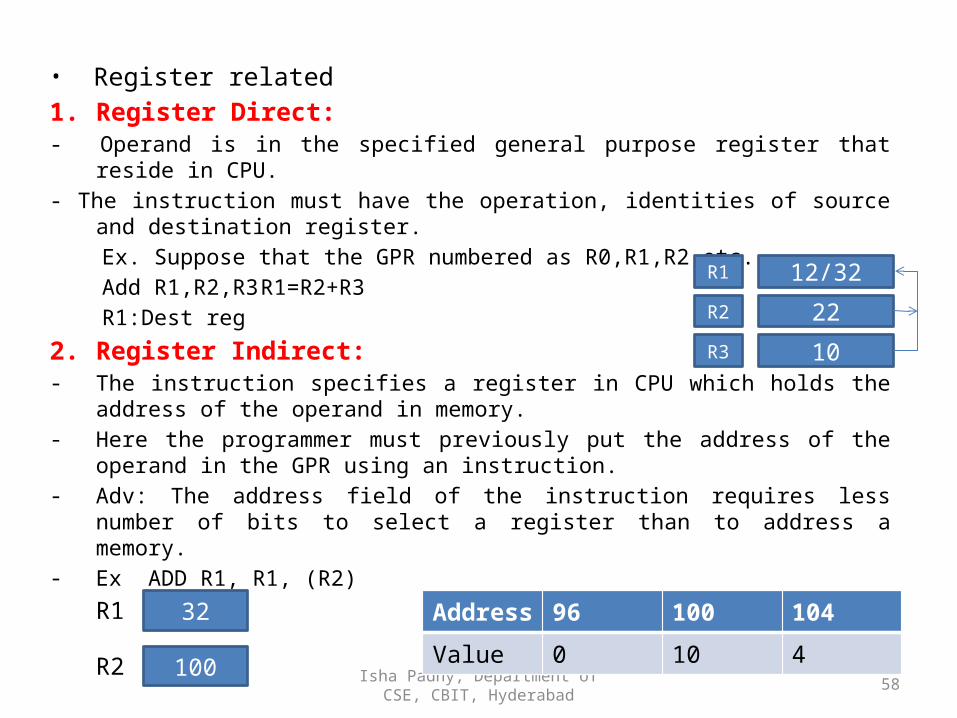
• Register related1. Register Direct: - Operand is in the specified general purpose register that reside in CPU.- The instruction must have the operation, identities of source and destination register. Ex. Suppose that the GPR numbered as R0,R1,R2 etc. Add R1,R2,R3 R1=R2+R3 R1:Dest reg2. Register Indirect:- The instruction specifies a register in CPU which holds the address of the
operand in memory.- Here the programmer must previously put the address of the operand in the GPR
using an instruction. - Adv: The address field of the instruction requires less number of bits to select a
register than to address a memory.- Ex ADD R1, R1, (R2)
12/32
22
10
R1
R2
R3
Address 96 100 104Value 0 10 4
32
100R2
R1
Isha Padhy, Department of CSE, CBIT, Hyderabad
59
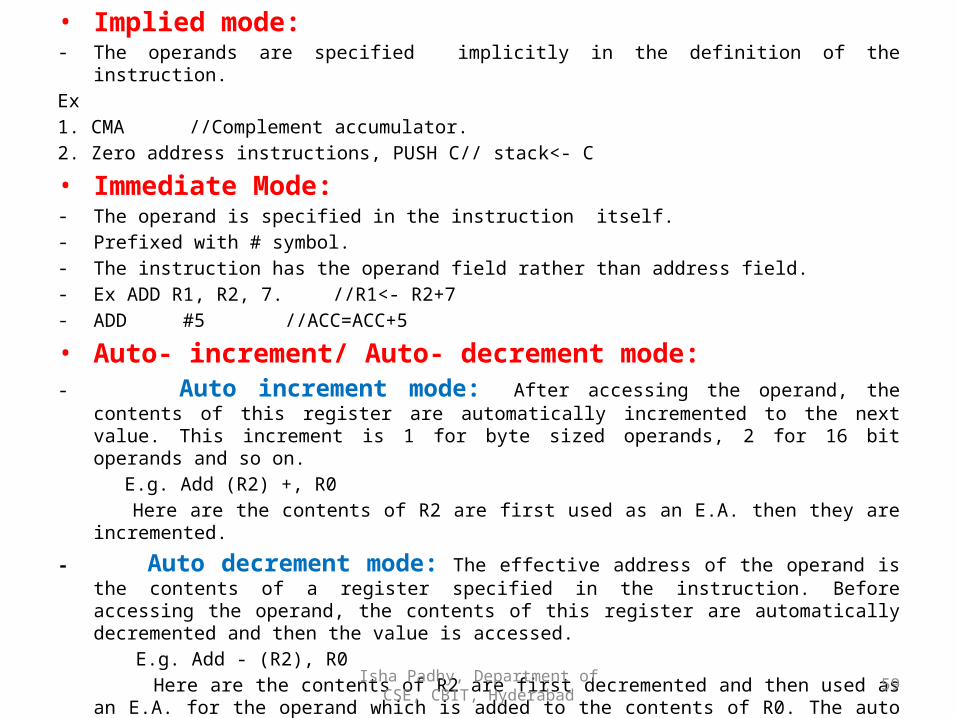
• Implied mode:- The operands are specified implicitly in the definition of the instruction.Ex1. CMA //Complement accumulator.2. Zero address instructions, PUSH C// stack<- C
• Immediate Mode:- The operand is specified in the instruction itself.- Prefixed with # symbol.- The instruction has the operand field rather than address field.- Ex ADD R1, R2, 7. //R1<- R2+7- ADD #5 //ACC=ACC+5• Auto- increment/ Auto- decrement mode:- Auto increment mode: After accessing the operand, the contents of this register are automatically
incremented to the next value. This increment is 1 for byte sized operands, 2 for 16 bit operands and so on. E.g. Add (R2) +, R0 Here are the contents of R2 are first used as an E.A. then they are incremented.
- Auto decrement mode: The effective address of the operand is the contents of a register specified in the instruction. Before accessing the operand, the contents of this register are automatically decremented and then the value is accessed.
E.g. Add - (R2), R0 Here are the contents of R2 are first decremented and then used as an E.A. for the operand which is added
to the contents of R0. The auto increment addressing mode and the auto decrement addressing mode are widely used for the implementation of data structures like Stack.
// The effective address of the operand is the contents of a register or main memory location, location whose address appears in the instruction.
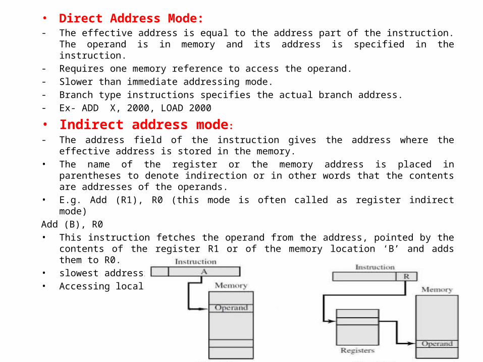
• Direct Address Mode: - The effective address is equal to the address part of the instruction. The operand is in memory and its
address is specified in the instruction.- Requires one memory reference to access the operand.- Slower than immediate addressing mode.- Branch type instructions specifies the actual branch address.- Ex- ADD X, 2000, LOAD 2000
• Indirect address mode:- The address field of the instruction gives the address where the effective address is stored in the
memory.• The name of the register or the memory address is placed in parentheses to denote indirection or in
other words that the contents are addresses of the operands.• E.g. Add (R1), R0 (this mode is often called as register indirect mode) Add (B), R0• This instruction fetches the operand from the address, pointed by the contents of the register R1 or of
the memory location ‘B’ and adds them to R0.• slowest addressing mode.• Accessing local variable like arrays and pointers.
Isha Padhy, Department of CSE, CBIT, Hyderabad 60
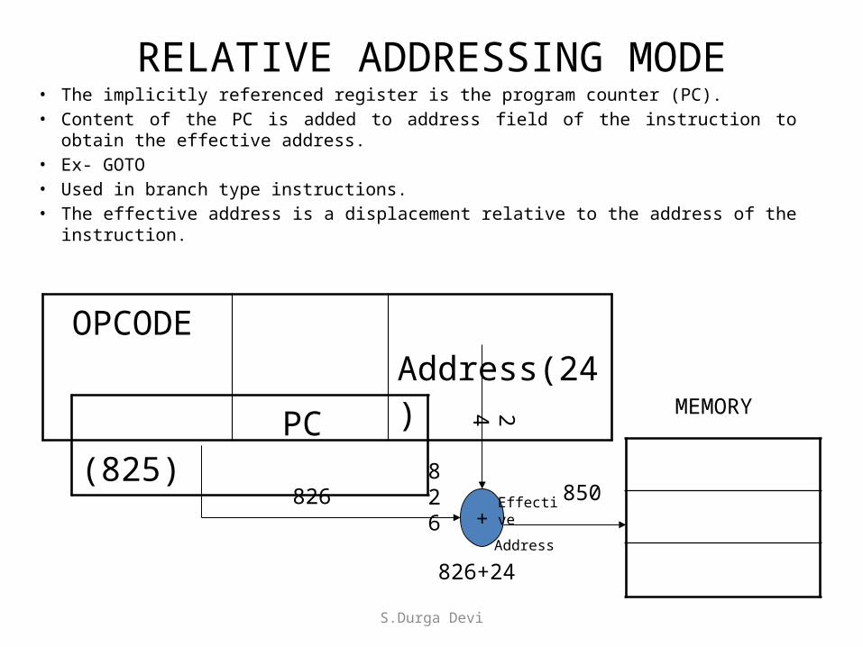
RELATIVE ADDRESSING MODE• The implicitly referenced register is the program counter (PC).• Content of the PC is added to address field of the instruction to obtain the effective
address.• Ex- GOTO • Used in branch type instructions.• The effective address is a displacement relative to the address of the instruction.
OPCODE Address(24)
PC (825)
+Address
Effective
MEMORY
826
24
826
826+24
850
S.Durga Devi
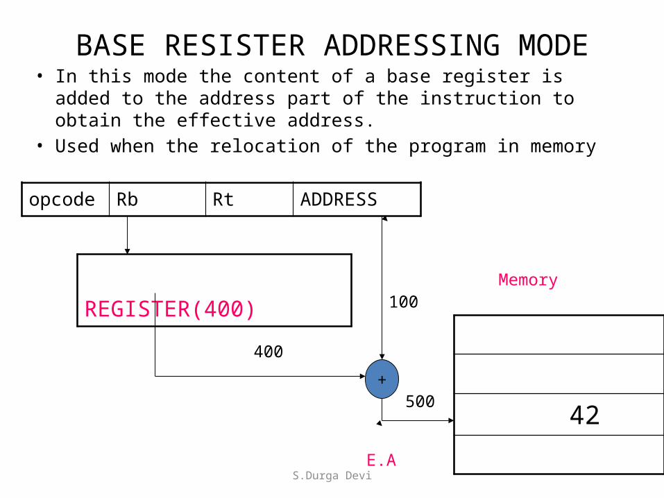
BASE RESISTER ADDRESSING MODE• In this mode the content of a base register is added to the
address part of the instruction to obtain the effective address.• Used when the relocation of the program in memory
opcode Rb Rt ADDRESS
REGISTER(400)
42
Memory
+
400
100
E.A
500
S.Durga Devi
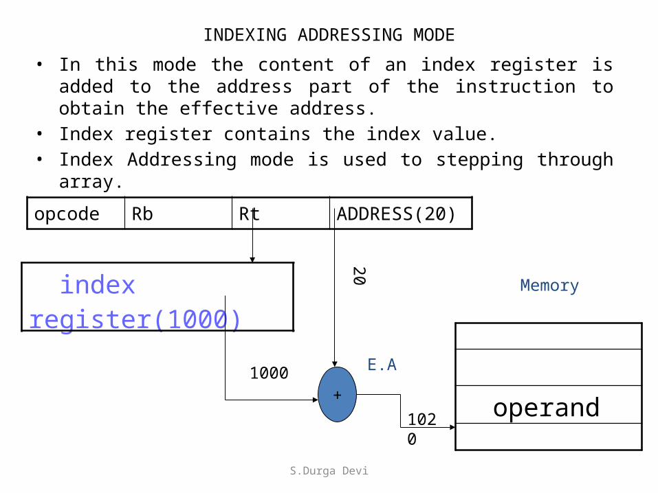
INDEXING ADDRESSING MODE
• In this mode the content of an index register is added to the address part of the instruction to obtain the effective address.
• Index register contains the index value.• Index Addressing mode is used to stepping through array.
opcode Rb Rt ADDRESS(20)
index register(1000)
operand+
1020
E.A1000
20Memory
S.Durga Devi
Isha Padhy, Department of CSE, CBIT, Hyderabad
64
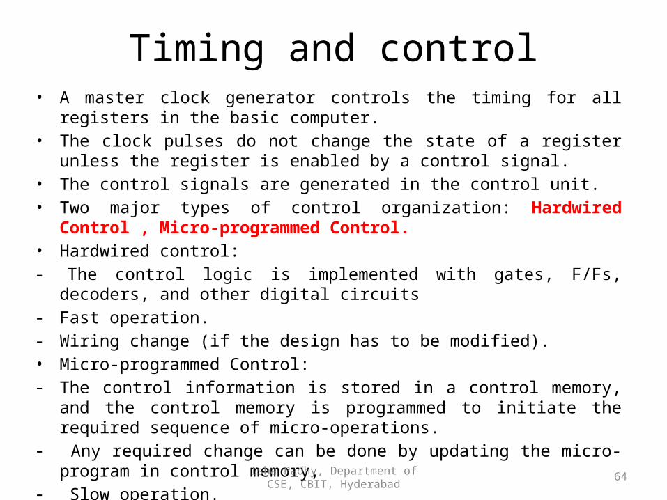
Timing and control• A master clock generator controls the timing for all registers in the basic computer.• The clock pulses do not change the state of a register unless the register is enabled
by a control signal.• The control signals are generated in the control unit.• Two major types of control organization: Hardwired Control , Micro-
programmed Control.• Hardwired control: - The control logic is implemented with gates, F/Fs, decoders, and other digital
circuits - Fast operation.- Wiring change (if the design has to be modified).• Micro-programmed Control:- The control information is stored in a control memory, and the control memory is
programmed to initiate the required sequence of micro-operations.- Any required change can be done by updating the micro-program in control
memory,- Slow operation.
Isha Padhy, Department of CSE, CBIT, Hyderabad
65
Isha Padhy, Department of CSE, CBIT, Hyderabad
66
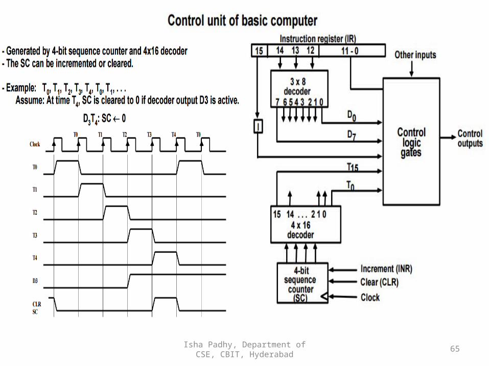
• The control unit consists of 2 decoders, 1 sequence counter, number of control logic gates.
• The instruction in IR is divide into 3 parts: 15 th bit to a FF called I, Operation code, and bits 0---11. The Op-code is decoded using 3*8 decoder(D0…D7).Bits 0..11 are applied to the control logic gates. The output of a 4-bit sequence counter are decoded into 16 timing signals (T0…T15).
• The SC responds to the positive transition of the clock. Initially CLR i/p is active, in 1st positive transition SC=0, timing signal T0 is active as the output of the decoder. This in turn triggers those registers whose control inputs are connected to T0. SC is incremented and the timing signals T0,T1,T2,T3.. .. are created. This continues unless SC is cleared. We can clear the SC with decoder output D3 active, denoted as:D3T4: SC<-0
• Output D3 from the operation decoder becomes active at the end of T2. when T4 is active, the output of AND gate that implements the control function D3T4 becomes active. This signal is applied to CLR input of SC.
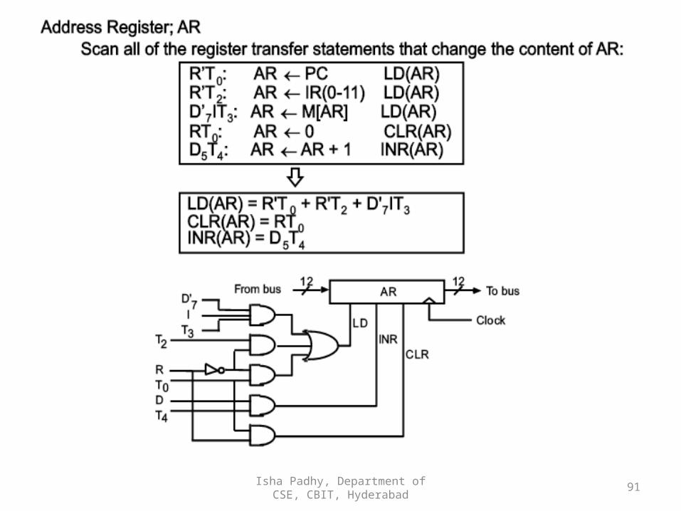
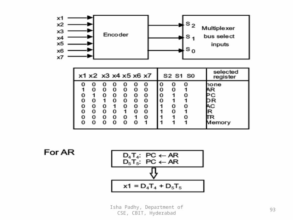
• Ex of register transfer: T0 : AR <- PC (Activities in T 0 will be, Content of PC placed on bus,S2S1S0 =010, LD of AR is active, transfer occurs at the end of positive transition, T0 is .inactive, T1 gets active)
Isha Padhy, Department of CSE, CBIT, Hyderabad
67
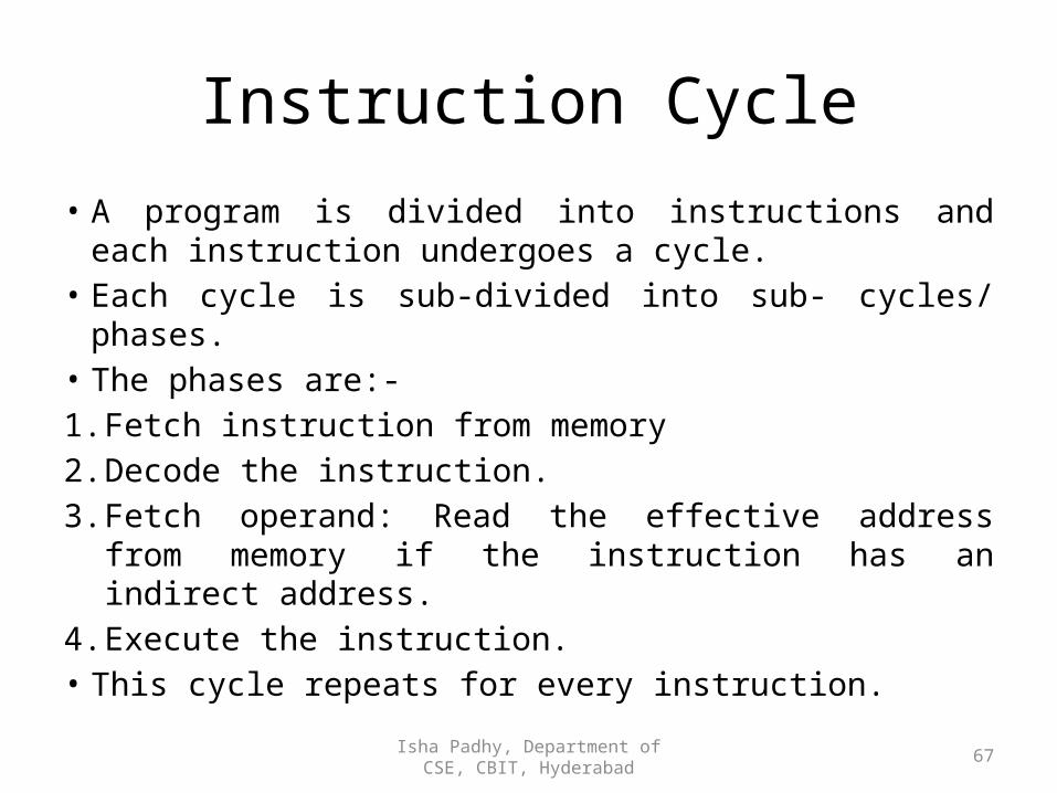
Instruction Cycle• A program is divided into instructions and each
instruction undergoes a cycle.• Each cycle is sub-divided into sub- cycles/ phases.• The phases are:-1. Fetch instruction from memory2. Decode the instruction.3. Fetch operand: Read the effective address from memory
if the instruction has an indirect address.4. Execute the instruction.• This cycle repeats for every instruction.
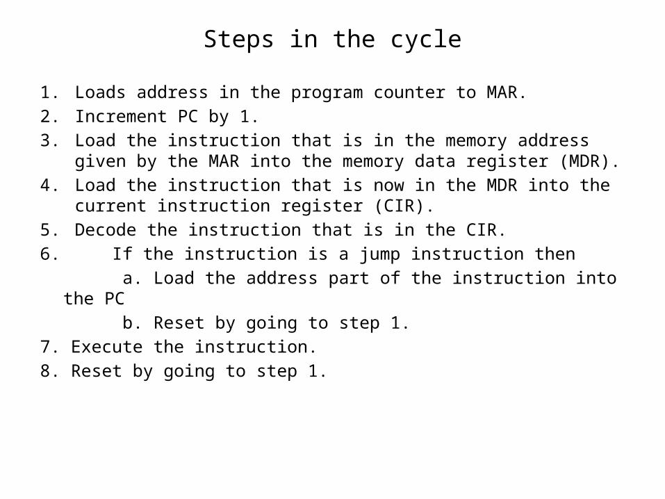
Steps in the cycle
1. Loads address in the program counter to MAR.2. Increment PC by 1.3. Load the instruction that is in the memory address given by the MAR
into the memory data register (MDR).4. Load the instruction that is now in the MDR into the current instruction
register (CIR).5. Decode the instruction that is in the CIR.6. If the instruction is a jump instruction then a. Load the address part of the instruction into the PC b. Reset by going to step 1.7. Execute the instruction.8. Reset by going to step 1.
Example - 1
Isha Padhy, Department of CSE, CBIT, Hyderabad
70
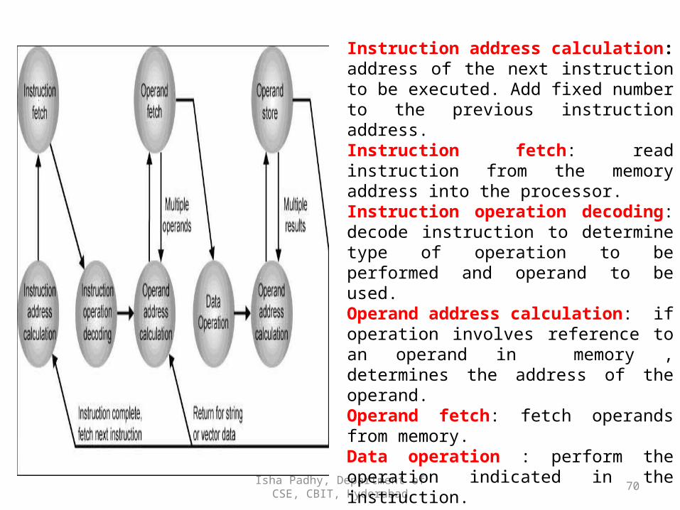
Instruction address calculation: address of the next instruction to be executed. Add fixed number to the previous instruction address.Instruction fetch: read instruction from the memory address into the processor.Instruction operation decoding: decode instruction to determine type of operation to be performed and operand to be used.Operand address calculation: if operation involves reference to an operand in memory , determines the address of the operand.Operand fetch: fetch operands from memory.Data operation : perform the operation indicated in the instruction.Operand store: write the result into memory .
Isha Padhy, Department of CSE, CBIT, Hyderabad
71
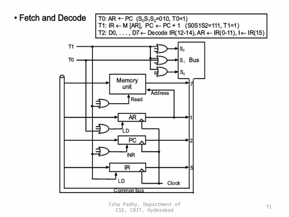
Isha Padhy, Department of CSE, CBIT, Hyderabad
72
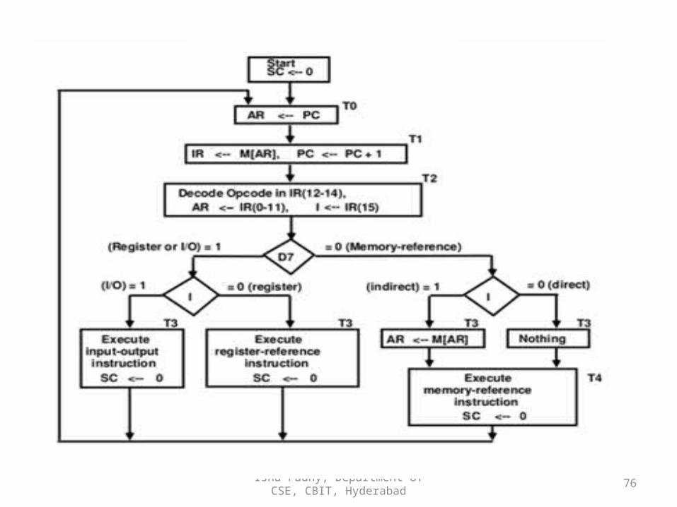
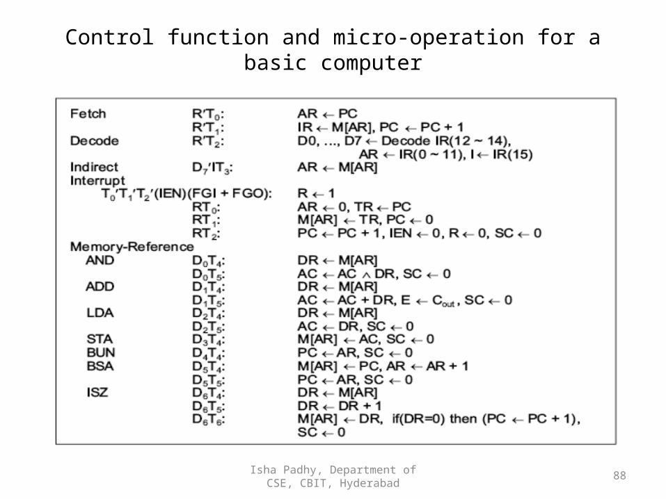
Fetch and Decode- PC holds the address of the 1st instruction.- SC is cleared to 0, the decoder output= T0.- T0: AR <- PC
T1: IR <- M[AR], PC <- PC +1T2: D0…..,D7 <- Decode IR(12-14),AR <- IR(0-11), I <- IR(15)
- At T0, place the contents of PC to bus by making S0S1S2=010. Transfer the contents of the bus to AR by enabling LD input.- At T1, IR <- M[AR], PC <- PC +1. 1. For this enable the read input of memory.2. Place the content of memory onto bus by S0S1S2= 1113. Transfer the content of the bus to IR by enabling LD input of IR.4. Increment PC by enabling the INR input of PC.- T0, T1 are connected to the control inputs of the registers, memory, bus selection inputs.
Address of the instruction transferred to AR
The opcode is decoded
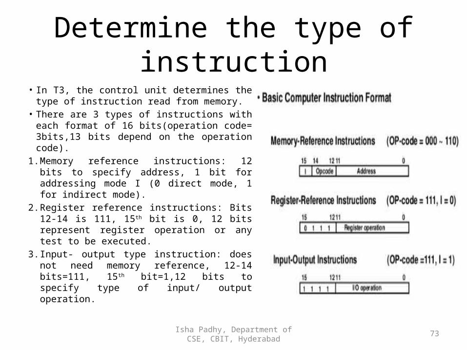
Determine the type of instruction• In T3, the control unit determines the type of
instruction read from memory.• There are 3 types of instructions with each
format of 16 bits(operation code= 3bits,13 bits depend on the operation code).
1. Memory reference instructions: 12 bits to specify address, 1 bit for addressing mode I (0 direct mode, 1 for indirect mode).
2. Register reference instructions: Bits 12-14 is 111, 15th bit is 0, 12 bits represent register operation or any test to be executed.
3. Input- output type instruction: does not need memory reference, 12-14 bits=111, 15th bit=1,12 bits to specify type of input/ output operation.
Isha Padhy, Department of CSE, CBIT, Hyderabad 73
Isha Padhy, Department of CSE, CBIT, Hyderabad
74
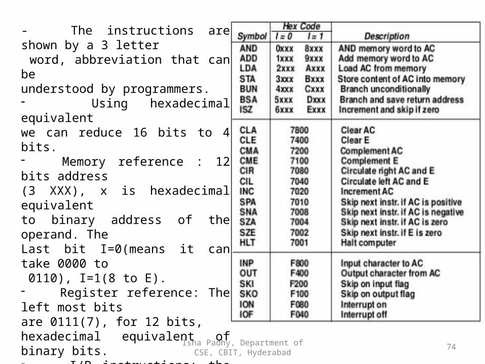
- The instructions are shown by a 3 letter word, abbreviation that can be understood by programmers.- Using hexadecimal equivalent we can reduce 16 bits to 4 bits.- Memory reference : 12 bits address (3 XXX), x is hexadecimal equivalent to binary address of the operand. The Last bit I=0(means it can take 0000 to 0110), I=1(8 to E).- Register reference: The left most bits are 0111(7), for 12 bits,hexadecimal equivalent of binary bits.- I/P instructions: the left most bits are 1111(F).
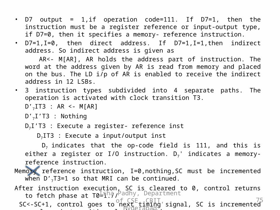
• D7 output = 1,if operation code=111. If D7=1, then the instruction must be a register reference or input-output type, if D7=0, then it specifies a memory- reference instruction.
• D7=1,I=0, then direct address. If D7=1,I=1,then indirect address. So indirect address is given as
AR<- M[AR], AR holds the address part of instruction. The word at the address given by AR is read from memory and placed on the bus. The LD i/p of AR is enabled to receive the indirect address in 12 LSBs.
• 3 instruction types subdivided into 4 separate paths. The operation is activated with clock transition T3.D’7IT3 : AR <- M[AR]D’7I’T3 : NothingD7I’T3 : Execute a register- reference inst
D7IT3 : Execute a input/output inst D7 indicates that the op-code field is 111, and this is either a register or I/O instruction. D7'
indicates a memory-reference instruction.Memory reference instruction, I=0,nothing,SC must be incremented when D’7T3=1 so that MRI
can be continued.After instruction execution, SC is cleared to 0, control returns to fetch phase at T0=1.// SC<-SC+1, control goes to next timing signal, SC is incremented or cleared at positive clock
transition.
Isha Padhy, Department of CSE, CBIT, Hyderabad 75
Isha Padhy, Department of CSE, CBIT, Hyderabad
76
Isha Padhy, Department of CSE, CBIT, Hyderabad
77
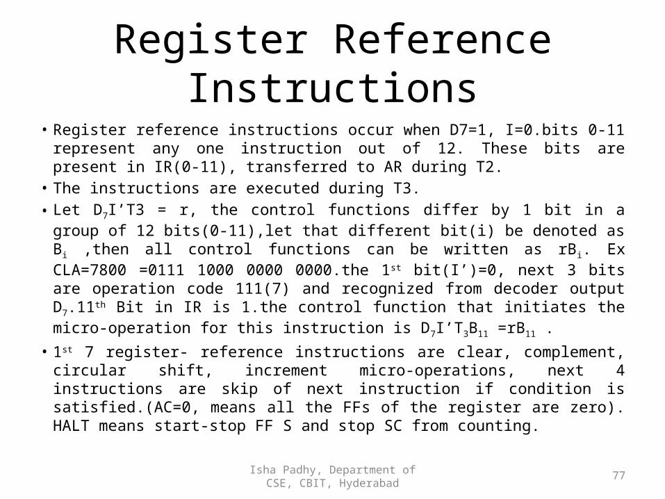
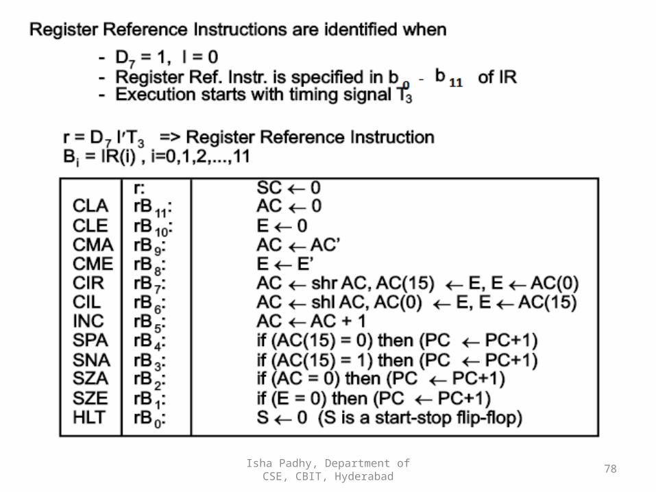
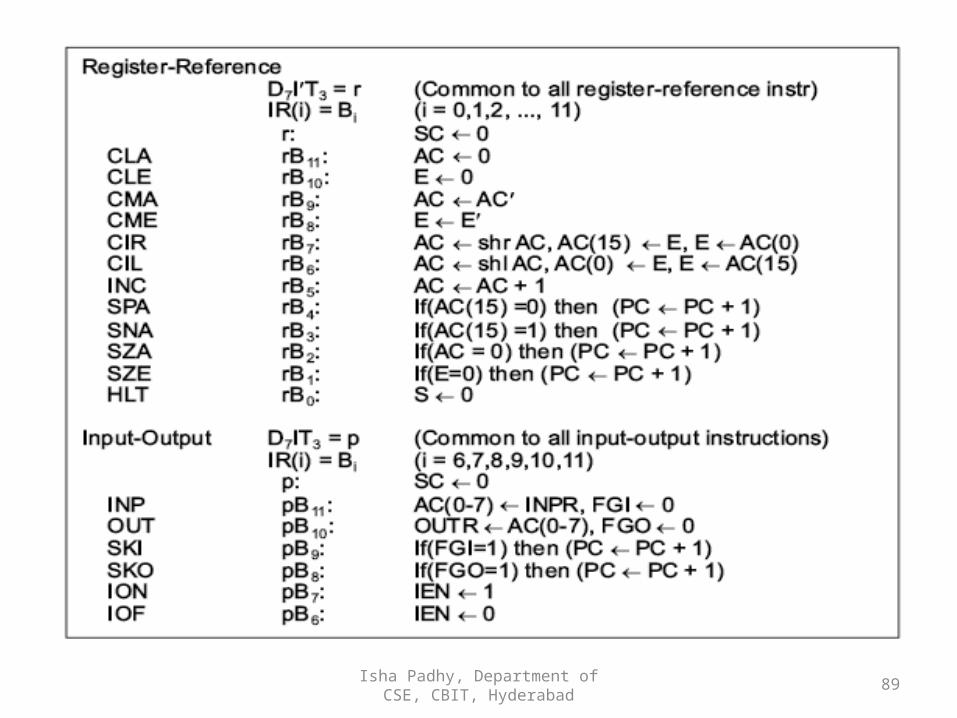
Register Reference Instructions• Register reference instructions occur when D7=1, I=0.bits 0-11 represent any
one instruction out of 12. These bits are present in IR(0-11), transferred to AR during T2.
• The instructions are executed during T3.• Let D7I’T3 = r, the control functions differ by 1 bit in a group of 12 bits(0-
11),let that different bit(i) be denoted as Bi ,then all control functions can be written as rBi. Ex CLA=7800 =0111 1000 0000 0000.the 1st bit(I’)=0, next 3 bits are operation code 111(7) and recognized from decoder output D7.11th Bit in IR is 1.the control function that initiates the micro-operation for this instruction is D7I’T3B11 =rB11 .
• 1st 7 register- reference instructions are clear, complement, circular shift, increment micro-operations, next 4 instructions are skip of next instruction if condition is satisfied.(AC=0, means all the FFs of the register are zero). HALT means start-stop FF S and stop SC from counting.
Isha Padhy, Department of CSE, CBIT, Hyderabad
78

Isha Padhy, Department of CSE, CBIT, Hyderabad
79
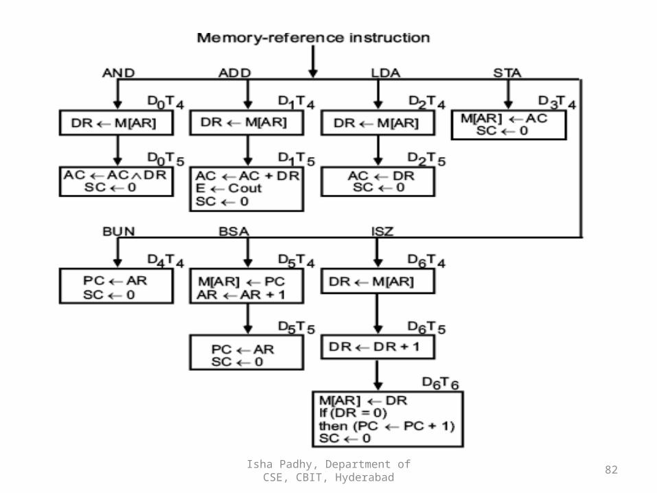
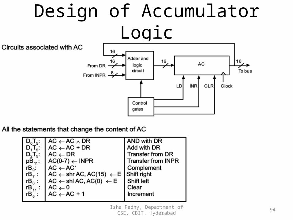
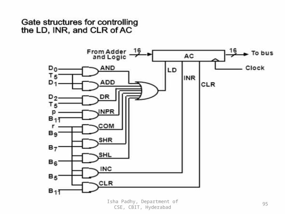
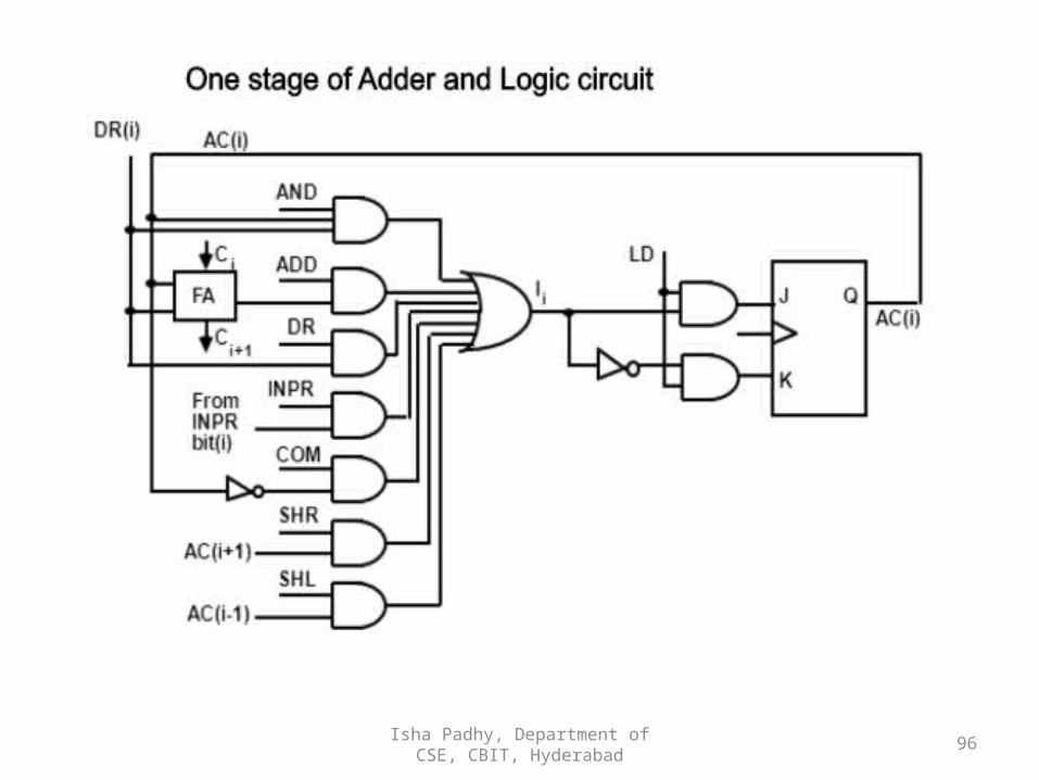
-AND, ADD must all be performed in two steps because AC can only be accessed via DR-E :extended accumulator flip flop, Carry bit is transferred to E-AR holds the effective address of the instruction duringT2 when I=0, T3 when I=1.- The execution of MRI starts at T4.
MEMORY REFERENCE INSTRUCTIONS
Isha Padhy, Department of CSE, CBIT, Hyderabad
80
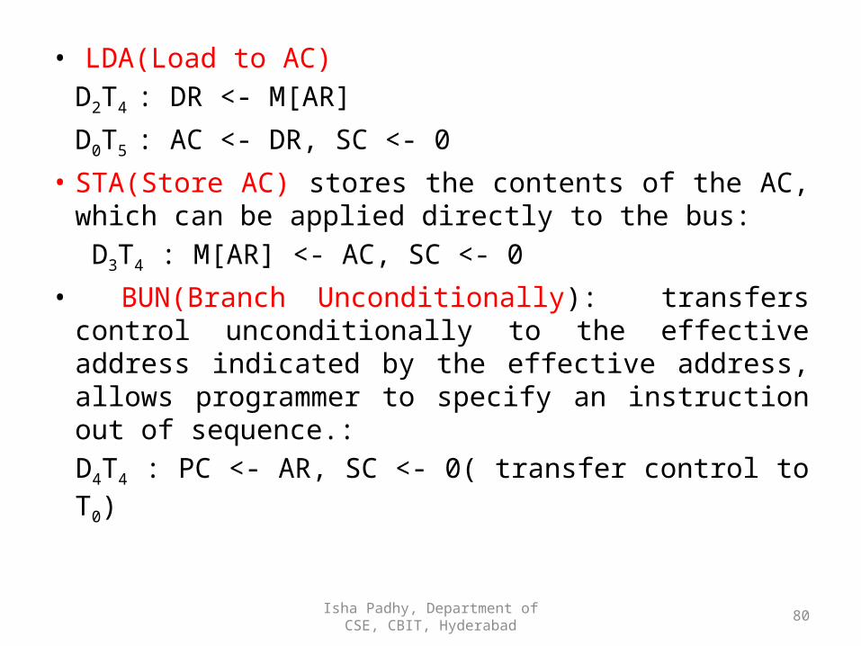
• LDA(Load to AC)D2T4 : DR <- M[AR] D0T5 : AC <- DR, SC <- 0
• STA(Store AC) stores the contents of the AC, which can be applied directly to the bus: D3T4 : M[AR] <- AC, SC <- 0
• BUN(Branch Unconditionally): transfers control unconditionally to the effective address indicated by the effective address, allows programmer to specify an instruction out of sequence.:
D4T4 : PC <- AR, SC <- 0( transfer control to T0)
Isha Padhy, Department of CSE, CBIT, Hyderabad
81
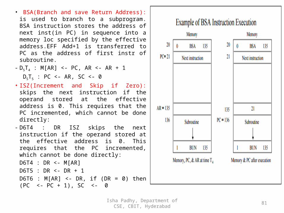
• BSA(Branch and save Return Address): is used to branch to a subprogram. BSA instruction stores the address of next inst(in PC) in sequence into a memory loc specified by the effective address.EFF Add+1 is transferred to PC as the address of first instr of subroutine.
- D5T4 : M[AR] <- PC, AR <- AR + 1 D5T5 : PC <- AR, SC <- 0
• ISZ(Increment and Skip if Zero): skips the next instruction if the operand stored at the effective address is 0. This requires that the PC incremented, which cannot be done directly:
- D6T4 : DR ISZ skips the next instruction if the operand stored at the effective address is 0. This requires that the PC incremented, which cannot be done directly: D6T4 : DR <- M[AR] D6T5 : DR <- DR + 1 D6T6 : M[AR] <- DR, if (DR = 0) then (PC <- PC + 1), SC <- 0
Isha Padhy, Department of CSE, CBIT, Hyderabad
82
Isha Padhy, Department of CSE, CBIT, Hyderabad
83
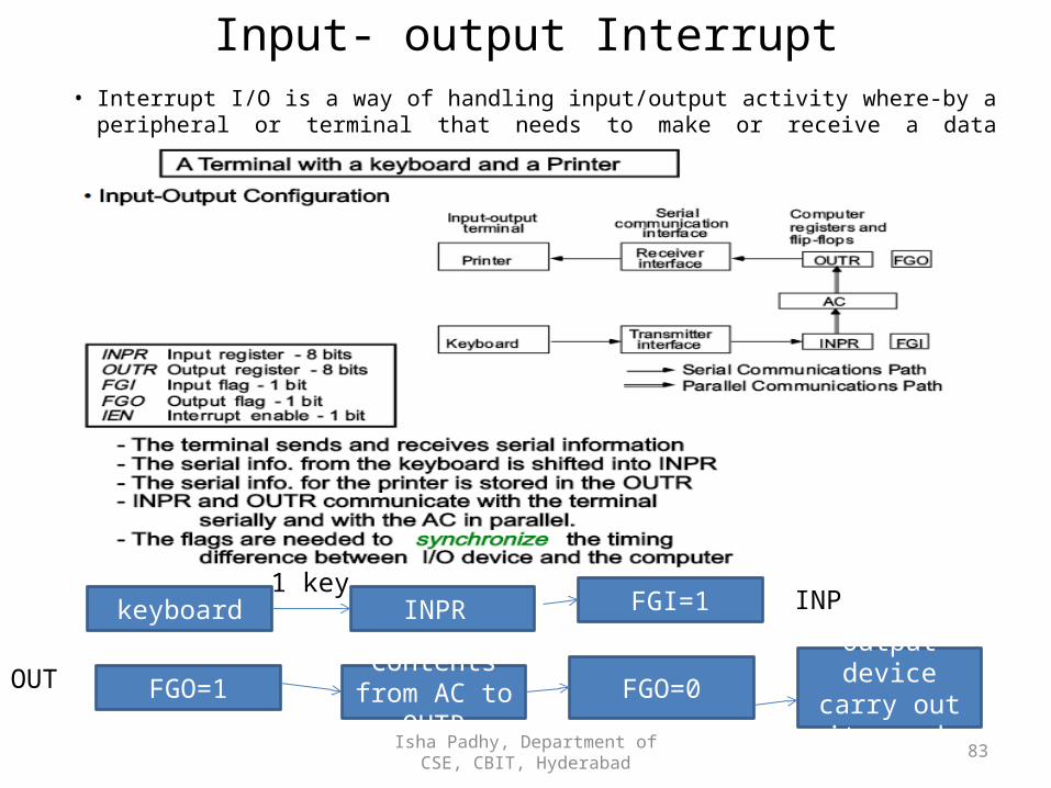
• Interrupt I/O is a way of handling input/output activity where-by a peripheral or terminal that needs to make or receive a data transfer sends a signal.
keyboard INPR FGI=11 key
FGO=1 Contents from AC to OUTR
FGO=0Output device
carry out its work
INP
OUT
Input- output Interrupt
Input- output Instructions
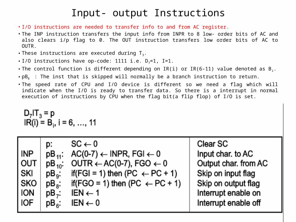
Isha Padhy, Department of CSE, CBIT, Hyderabad 84
• I/O instructions are needed to transfer info to and from AC register.• The INP instruction transfers the input info from INPR to 8 low- order bits of AC and also clears i/p
flag to 0. The OUT instruction transfers low order bits of AC to OUTR.• These instructions are executed during T3.• I/O instructions have op-code: 1111 i.e. D7=1, I=1.• The control function is different depending on IR(i) or IR(6-11) value denoted as B i.• pB8 : The inst that is skipped will normally be a branch instruction to return.• The speed rate of CPU and I/O device is different so we need a flag which will indicate when the I/O is
ready to transfer data. So there is a interrupt in normal execution of instructions by CPU when the flag bit(a flip flop) of I/O is set.
Isha Padhy, Department of CSE, CBIT, Hyderabad
85
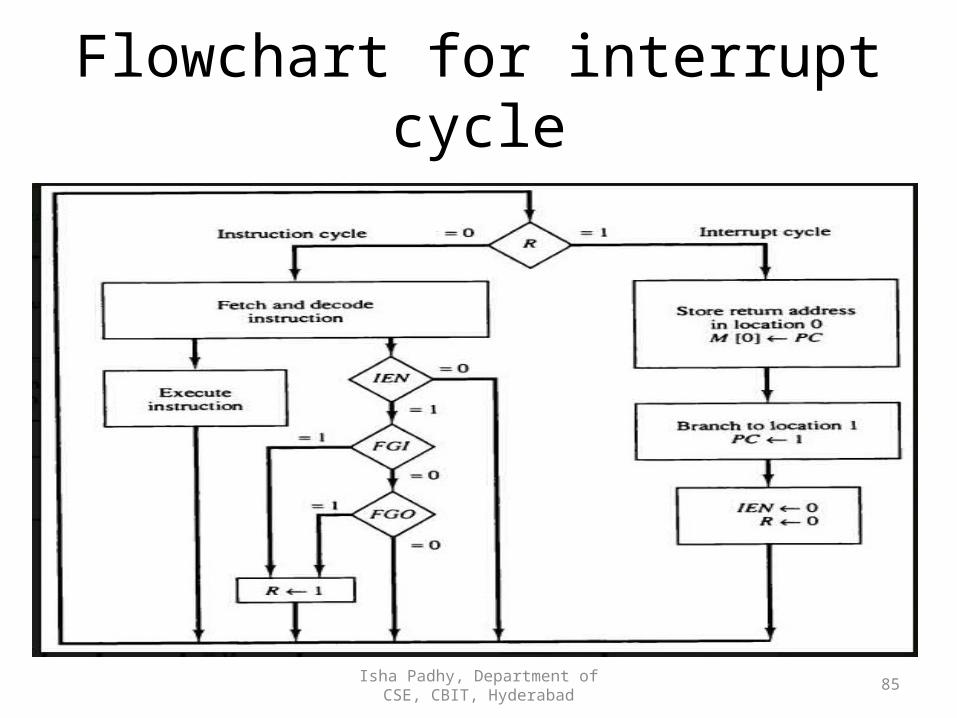
Flowchart for interrupt cycle
Isha Padhy, Department of CSE, CBIT, Hyderabad
86
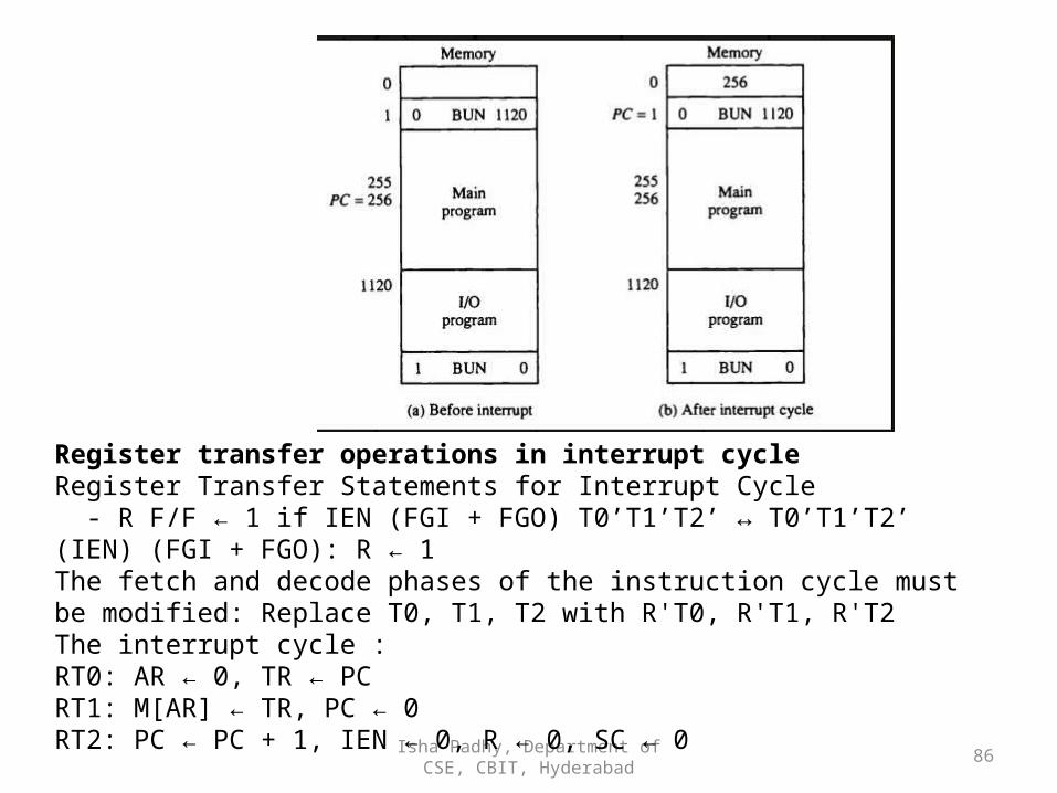
Register transfer operations in interrupt cycleRegister Transfer Statements for Interrupt Cycle - R F/F ← 1 if IEN (FGI + FGO) T0’T1’T2’ ↔ T0’T1’T2’ (IEN) (FGI + FGO): R ← 1The fetch and decode phases of the instruction cycle must be modified: Replace T0, T1, T2 with R'T0, R'T1, R'T2The interrupt cycle : RT0: AR ← 0, TR ← PCRT1: M[AR] ← TR, PC ← 0RT2: PC ← PC + 1, IEN ← 0, R ← 0, SC ← 0
Isha Padhy, Department of CSE, CBIT, Hyderabad
87
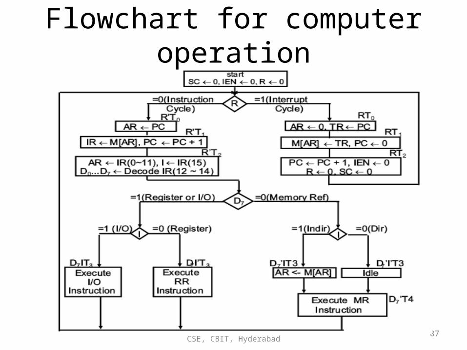
Flowchart for computer operation
Isha Padhy, Department of CSE, CBIT, Hyderabad
88
Control function and micro-operation for a basic computer
Isha Padhy, Department of CSE, CBIT, Hyderabad
89
Isha Padhy, Department of CSE, CBIT, Hyderabad
90
Isha Padhy, Department of CSE, CBIT, Hyderabad
91

Isha Padhy, Department of CSE, CBIT, Hyderabad
92
Isha Padhy, Department of CSE, CBIT, Hyderabad
93
Isha Padhy, Department of CSE, CBIT, Hyderabad
94
Design of Accumulator Logic
Isha Padhy, Department of CSE, CBIT, Hyderabad
95
Isha Padhy, Department of CSE, CBIT, Hyderabad
96
Recommended


![COMPUTER ORGANIZATION Subject Code: 10CS46 - VTU Solutionvtusolution.in/.../cse-iii-computer__organization_[15cs34]-notes.pdf · COMPUTER ORGANIZATION 10CS46 . COMPUTER ORGANIZATION](https://img.pdfslide.net/doc/110x75/5b7970717f8b9a331e8dcaf3/computer-organization-subject-code-10cs46-vtu-15cs34-notespdf-computer.jpg)