CONTROL OF NUCLEATION AND GRAIN
GROWTH IN SOLID-PHASE CRYSTALLIZED
SILICON FOR HIGH-PERFORMANCE THIN FILM
TRANSISTORS
A DISSERTATION SUBMITTED TO THE
DEPARTMENT OF ELECTRICAL ENGINEERING
AND THE COMMITTEE OF GRADUATE STUDIES
OF STANFORD UNIVERSITY IN PARTIAL
FULFULLMENT OF THE REQUIREMENTS FOR
THE DEGREE OF DOCTOR OF PHILOSOPHY
Vivek Subramanian
June 1998.

ii
© Copyright by Vivek Subramanian 1998
All Rights Reserved
iii
I certify that I have read this dissertation and that in my
opinion it is fully adequate, in scope and quality, as a
dissertation for the degree of Doctor of Philosophy.
____________________________________
Krishna C. Saraswat
(Principle Adviser)
I certify that I have read this dissertation and that in my
opinion it is fully adequate, in scope and quality, as a
dissertation for the degree of Doctor of Philosophy.
____________________________________
James D. Plummer
I certify that I have read this dissertation and that in my
opinion it is fully adequate, in scope and quality, as a
dissertation for the degree of Doctor of Philosophy.
____________________________________
Richard A. Kiehl
Approved for the University Committee on Graduate
Studies:
____________________________________

iv

v
Abstract
___________________________________________
Thin film transistors (TFTs) are used as pixel switches in active matrix liquid
crystal displays (AMLCDs). Polycrystalline TFTs may allow driver integration onto the
display substrate, reducing overall cost. High-performance poly-TFTs may allow the
vertical integration of devices for VLSI, increasing packing density and improving
performance through reduced interconnect delay.
Poly-TFT channels are conveniently formed through the solid-phase
crystallization (SPC) of amorphous silicon. Unfortunately, such films are usually of poor
quality, having small grains. The need exists for a means of forming large grains using
SPC.
SPC occurs through nucleation and subsequent grain growth. Large grains are
formed when nucleation is minimized. By manipulating the relative rates of nucleation
and grain growth, high-performance TFTs may be fabricated. In this work, the
mechanisms of deposition and crystallization have been studied experimentally and
theoretically. This knowledge has been used to develop technologies for the
manipulation of nucleation and grain growth.
To facilitate crystallization studies, an acoustic crystallinity sensor has been
developed. Using this, a two-step crystallization process has been demonstrated that
improves process throughput and device performance. A high-temperature nucleation
step is used to reduce incubation time, followed by a low-temperature growth step to
maximize grain size.
The ideal TFT would have a single grain only. This requires an ability to control
grain location. Two techniques to achieve this have been developed. In the first
technique, heating is locally increased in the TFT electrode regions by using overlying
light absorption masks during an initial rapid thermal anneal step, resulting in selective
nucleation. These nuclei are then enlarged laterally at low temperature. In the second
technique, germanium is alloyed with the film in the electrodes to induce nucleation, and
the resulting nuclei are laterally crystallized. Both techniques result in the formation of
vi
large-grain spatially-specified polysilicon, achieved solely through the manipulation of
nucleation and grain-growth. This has enabled the fabrication of high-performance
TFTs. The techniques may even enable the fabrication of single-grain transistors, having
performance approaching that of bulk devices. The potential therefore exists for the
integration of driver circuitry in AMLCDs and for the fabrication of vertically integrated
circuits for advanced VLSI applications.

vii
Acknowledgements
___________________________________________
I would like to thank several people who have made this work possible, and who
have made my years at Stanford enjoyable. First and foremost, I would like to thank my
advisor, Prof. Krishna C. Saraswat, for all his guidance and support. Prof. Saraswat gave
me the freedom to pursue my interests while simultaneous keeping me on track and
focused. I would also like to thank my associate advisor, Prof. Jim Plummer, for his
useful advice and encouragement, and Dr. Jim McVittie and Prof. Fraser-Smith for
serving on my orals committee, and Dr. Rick Kiehl for serving on my reading committee.
This work is inherently experimental, and would not have been possible without
the support of the staff of the Stanford Nanofabrication Facility. Thanks go to Keith
Gaul, for maintaining the SiGe deposition system, and to Len Booth, for maintaining and
operating the Stanford Rapid Thermal Multiprocessor. Thanks also go to Pat Burke for
all his help with the ultratech. I would also like to thank Bob Wheeler for his
administrative support. Bob vocally supported me whenever I wanted to upgrade the
SiGe deposition system, and without his help, the system would not be the flexible
machine it is today. Thanks also go to Karl Brandt, Luke Eisenbach, and Bill Martin for
their help in keeping the lab up and running. The camaraderie I developed with the
maintenance staff made my years in the SNF enjoyable beyond measure.
I would also like to thank the process staff for all their assistance in the lab. I
would like to thank Gladys Sarmiento for running literally hundreds of implants for me
over the last four years, Margaret Prisbe for help with general processing, and Marnel
King for all her help with the e-beam. Thanks also go to Robin King and Nancy Latta for
all their help, and to Paul Jerabek, for making the numerous ultratech plates I have used.
I have interacted with numerous people at CIS through the years, including Joe
Little and Bill Murray. To them go my sincere thanks. Thanks also go to my friends
Nabeel Ibrahim, Jim Schneider, Patrick Yue, and Hung Chen, who dragged me out of the
lab occasionally for coffee, BBQ, bowling, squash and beer. I would like to thank the
numerous members of Prof. Saraswat’s device group, past and present, who have

viii
provided me with help and advice through the years, including Tsu-Jae King, Albert
Wang, Navakanta Bhat, Dan Connelly, Steve Jurichich, Shukri Souri, T. C. Yang, and
Amol Joshi. Thanks especially to Irene Sweeney for her tireless administrative support
on my behalf.
Through the course of this work, I have collaborated with numerous people at
Stanford, including Madan Kumar, Paul Dankosksi, Levent Degertekin, Ann Marshall,
and Glenn Waychunas. They have my gratitude. I would also like to thank Jackson Ho
of Xerox Corporation for all his help with device fabrication, and Dave Williams, Ching
Tang, Ling-Sung Hung, Gary Bottger and Jim Pearson of Eastman Kodak Company for
their support, financial and otherwise. Thanks to John Mehlhaff and Howard
Hovagimian for the opportunities they provided me with early in my Ph.D. The
interaction with them in many ways laid the foundation for this work. I would also like
to thank Bich-Yen Nguyen, Phil Tobin, Bill Taylor, and James Smith of Motorola
APRDL for the wonderful and enlightening summer I spent at Motorola. Thanks also to
DARPA for the continuous support of this project.
Finally, thanks go to my family for providing me with such strong support and
love through the years. Thanks go to my parents and sister for being there for me, and for
just being the wonderful family that they are. Thanks to my wife, Yvette, for her love
and support through the years, and for giving me a smiling, loving face to go home to
after a tough day in the lab. Thanks to my loving cocker spaniel, Rufus, who is
unquestionably the best friend, brother, and companion I could ever ask for.
ix
Table of Contents
___________________________________________
Abstract.......................................................................................................... v
Acknowledgements ..................................................................................... vii
Chapter 1: Introduction ............................................................................... 1
1.1: TFTs: a historical perspective............................................................................... 1
1.2: Applications of thin film transistors ..................................................................... 3
1.2.1: Active matrix liquid crystal displays .......................................................... 3
1.2.2: Vertical integration of active devices ......................................................... 6
1.3: Methodology of study ........................................................................................... 8
1.4: Organization.......................................................................................................... 9
Chapter 2: The Chemical Vapor Deposition and Solid-Phase
Crystallization of Amorphous Silicon....................................................... 11
2.1: Low-pressure chemical vapor deposition of silicon films .................................. 12
2.1.1: Process chemistry..................................................................................... 13
2.1.2: Adsorption processes................................................................................ 15
2.1.3: Initial nucleation on amorphous substrates ............................................. 18
2.1.4: Deposition process ................................................................................... 22
2.1.5: Unified description of amorphous silicon deposition............................... 25
2.2: Solid-phase crystallization of amorphous silicon ............................................... 28
2.2.1: Thermodynamic considerations of nucleation and growth ...................... 28
2.2.2: Effect of pre-existing nuclei on grain size ................................................ 36
2.3: Unification of deposition and crystallization models ......................................... 38
2.4: Defects in solid-phase crystallized polysilicon films.......................................... 45
2.5: Conclusions......................................................................................................... 47
Chapter 3: Detection of nucleation and crystallization in amorphous
silicon............................................................................................................ 49
x
3.1: Background information ..................................................................................... 50
3.1.1: Rapid thermal crystallization ................................................................... 50
3.1.2: Measurement principles ........................................................................... 51
3.2: Experimental methodology................................................................................. 53
3.3: Results and discussion ........................................................................................ 56
3.4: Conclusions......................................................................................................... 60
Chapter 4: Improvement of process throughput in solid-phase
crystallized TFTs using two-step annealing..............................................63
4.1: Conceptual basis for multi-step annealing.......................................................... 63
4.2: Experimental methodology................................................................................. 64
4.3: Results and discussion ........................................................................................ 65
4.4: Conclusions......................................................................................................... 69
Chapter 5: Laterally crystallized polysilicon TFTs for AMLCD
applications using patterned light absorption masks ..............................71
5.1: Conceptual basis for patterned absorption masking ........................................... 72
5.2: Experimental details............................................................................................ 74
5.3: Results and discussion ........................................................................................ 75
5.4: Conclusions......................................................................................................... 84
Chapter 6: Optimization of amorphous precursor characteristics of
silicon-germanium alloys ............................................................................85
6.1: Background information ..................................................................................... 86
6.1.1: Silicon-germanium deposition.................................................................. 86
6.1.2: Design of experiments .............................................................................. 87
6.2: Experimental details............................................................................................ 89
6.3: Results and discussion ........................................................................................ 90
6.4: Conclusions....................................................................................................... 100
Chapter 7: Germanium-seeded laterally crystallized TFTs for vertical
integration of MOSFETs ..........................................................................101
7.1: Conceptual basis for germanium-seeding......................................................... 102

xi
7.2: Experimental details.......................................................................................... 103
7.3: Results and discussion ...................................................................................... 104
7.4: Conclusions....................................................................................................... 111
Chapter 8: Conclusions ............................................................................ 113
8.1: Summary........................................................................................................... 113
8.1.1: Theory of deposition and solid phase crystallization ............................. 114
8.1.2: Detection of nucleation and crystallization in amorphous silicon......... 114
8.1.3: Experimental demonstration of controlled nucleation and growth........ 115
8.2: Recommendations for future work ................................................................... 117
Appendix 1: The Effect of Defects on Electron Transport in
Polycrystalline Silicon-based Devices ..................................................... 119
A1.1: A model of electron trapping in grain boundaries ......................................... 119
A1.2: Electron conduction in polycrystalline thin film transistors .......................... 122
Appendix 2: Thin Film Transistor Fabrication Processes.................... 125
A2.1: Low-temperature TFT fabrication process .................................................... 125
A2.2: Differences between low- and high- temperature processes.......................... 128
Bibliography .............................................................................................. 131

xii

xiii
List of Tables
___________________________________________
2-1: Survey of crystallization activation energies. ............................................................ 33
4-1: Summary of device characteristics ............................................................................ 68
5-1: Device characteristics for 2µm/2µm TFTs................................................................ 76
5-2: Thermal and electrical analogues .............................................................................. 80
6-1: Comparison of theoretical and experimental mobility values. .................................. 91
6-2: Summary of device characteristics ............................................................................ 94
7-1: Summary of device characteristics (W/L=0.9µm/0.7µm)....................................... 107
7-2: Summary of intra-wafer mobility uniformity (W/L=0.9µm/0.7µm)....................... 108

xiv

xv
List of Figures
___________________________________________
1.1: Conceptualization of TFT from Heil’s 1943 patent specification ............................... 2
1.2: Passive matrix addressing scheme. .............................................................................. 3
1.3: Active matrix addressing scheme................................................................................. 4
1.4: Structure of a color AMLCD ....................................................................................... 5
1.5: Inverted-staggered amorphous silicon TFT ................................................................. 5
1.6: Top-gate self-aligned planar TFT ................................................................................ 6
1.7: Standard and vertically integrated inverter cells.......................................................... 7
1.8: Conventional and vertically integrated circuit ............................................................. 8
2.1: Schematic view of silicon deposition process............................................................ 14
2.2: Potential energy vs. distance from adsorption site for silicon deposition.................. 15
2.3: Growth rate of silicon as a function of temperature................................................... 23
2.4: Structure of deposited film......................................................................................... 27
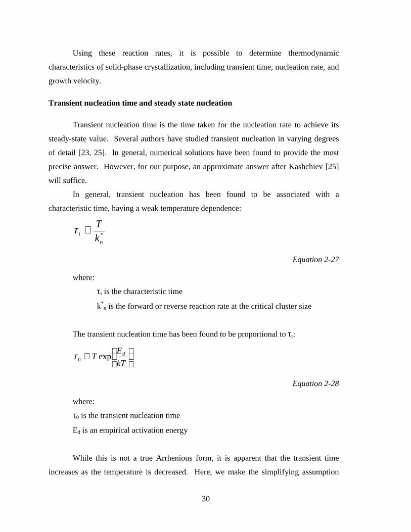
2.5: Regimes of nucleation during solid-phase crystallization ......................................... 32
2.6: Variation in nucleation and growth with crystallization temperature........................ 36
2.7: Temperature dependence of nucleation and growth .................................................. 39
2.8: Fitting of model to crystallite size data from Aoyama et al ....................................... 40
2.9: Theoretical and experimental variation in device mobility with crystallization
temperature................................................................................................................. 44
2.10: Configuration of elliptical crystallites, showing formation of (11) twin planes ...... 46
3.1: Cross section of acoustic sensor system..................................................................... 51
3.2: Thermodynamic properties of the system, showing film-dependent absorption ....... 53
3.3: Cross section of Stanford Rapid Thermal Multiprocessor......................................... 54
3.4: Time of flight curves for low and high lamp powers relative to time of flight at
room temperature ....................................................................................................... 55
3.5: Temperature vs. time curves for annealing of initially amorphous and
polycrystalline films................................................................................................... 57
3.6: TEM and SAD for sample annealed to “A”: amorphous........................................... 58
3.7: TEM and SAD for sample annealed to “B”: crystallite formation ............................ 58

xvi
3.8: TEM and SAD for sample annealed to “C”: partial crystallization........................... 59
3.9: TEM and SAD for sample annealed to “D”: complete crystallization ...................... 59
3.10: Progressive tightening of diffraction rings............................................................... 60
4.1: Thermal cycles used during various crystallization anneals ...................................... 65
4.2: Plan-view TEM showing film at start of quench in two-step process ....................... 66
4.3: Electrical transfer characteristics for PMOS TFTs .................................................... 67
4.4: Electrical transfer characteristics of NMOS TFTs..................................................... 67
5.1: Silicon absorption and radiant spectra for typical RTA lamps .................................. 72
5.2: Heat flow during RTA using patterned absorption masks ......................................... 73
5.3: Process flow for laterally crystallized TFTs (inset: TEM of seeded grain growth)... 75
5.4: Electrical characteristics of 2µm/2µm TFTs.............................................................. 76
5.5: Electrical characteristics of 20µm/20µm NMOS TFTs. ............................................ 77
5.6: Variation in NMOS field effect mobility with channel length .................................. 78
5.7: Variation in NMOS field-effect mobility improvement with device size.................. 78
5.8: Plan-view of mask structures to achieve (a) standard (b) laterally crystallized (c)
small grain (d) large-grain TFTs................................................................................ 80
5.9: Extraction of electrical equivalent of heat flow ......................................................... 81
6.1: Definition of experimental design space.................................................................... 88
6.2: Cross-section of SiGe TFT......................................................................................... 89
6.3 Response surface of NMOS mobility.......................................................................... 91
6.4: Response surface of PMOS mobility ......................................................................... 92
6.5: Transfer characteristic of sample NMOS TFT........................................................... 93
6.6: Transfer characteristics of sample PMOS TFTs ........................................................ 93
6.7: Schematic view of atomistic deposition model.......................................................... 95
6.8: Characterization of onset of gas-phase nucleation in Si and Si0.8Ge0.2...................... 97
6.9: Schematic view of (a) gas-phase nucleation and (b) the effect of Ge catalysis on
the same...................................................................................................................... 97
7.1: Process flow for Ge-seeded laterally crystallized TFT fabrication.......................... 103
7.2: AFM image showing polycrystalline seed points after defect etcha........................ 104
7.3: Plan-view TEM showing growth of seeded grains with seed structure boundary
overlaid in white....................................................................................................... 105

xvii
7.4: Electrical characteristics of NMOS TFTs (W/L=0.9µm/0.7µm)............................. 106
7.5: Electrical characteristics of PMOS TFTs (W/L=0.9µm/0.7µm) ............................. 106
7.6: Variation in NMOS field-effect mobility with channel length ................................ 107
7.7: Variation in NMOS mobility improvement with device size .................................. 108
7.8: NMOS mobility distributions for seeded and unseeded devices ............................ 109
7.9: Schematic view of lateral crystallization in the device channel .............................. 110
A1. 1: Grain structure, charge distribution and band diagram assumed in grain
boundary trapping model ......................................................................................... 120
A1. 2: Mechanism of leakage in polycrystalline TFTs ................................................... 122
A2. 1: Cross-section of wafer after channel deposition and crystallization.................... 125
A2. 2: Cross-section of device after active island patterning.......................................... 126
A2. 3: Cross-section of device after gate oxide deposition............................................. 126
A2. 4: Cross-section of device after gate electrode deposition ....................................... 126
A2. 5: Cross-section of device after gate patterning ....................................................... 126
A2. 6: Cross-section of device after terminal implantation ............................................ 127
A2. 7: Cross-section of device after deposition of passivation oxide ............................. 127
A2. 8: Cross-section of device after contact hole formation........................................... 127
A2. 9: Cross-section of device after metal deposition .................................................... 128
A2. 10: Cross-section of finished device ........................................................................ 128

xviii

1
Chapter 1
Introduction
___________________________________________
Polycrystalline silicon thin film transistors (TFTs) have received attention in
recent years because of their increasing use in active matrix liquid crystal displays
(AMLCDs). The ability to fabricate high-performance TFTs may enable their use in a
wide range of new applications, including microelectronic circuits. Thus, there is great
interest in improving the performance of polycrystalline TFTs. The goal of this work is
to study the basic physics of various processes used in the fabrication of polycrystalline
TFTs, and to exploit these phenomena to develop elegant means of improving TFT
performance. In this chapter, a historical perspective of TFTs is provided. Then the
applications of TFTs in modern microelectronics are reviewed. Next, a generalized
methodology of study as used in this work is introduced, providing the motivation for this
work. This is used to develop the organization of subsequent chapters.
1.1: TFTs: a historical perspective
Thin film transistors were among the first semiconductor-based three-terminal
electronic devices ever described. Indeed, the first U.S. patent on thin film transistors
was issued in 1933 [1], and the first European patent was issued one year later [2]. The
conceptualization of the thin film transistor from Heil’s 1934 patent is shown below
(Figure 1.1). The materials originally proposed for use in thin film transistors were
polycrystalline films of tellurium and various II-VI compounds. With the passage of
time, however, research on thin film transistors was superseded by work on point contact
devices, culminating in the development of the bipolar junction transistor at Bell labs [3].
After the initial success of the bipolar junction transistor, research on field-effect devices
reemerged in the late 1950s and early 1960s [4], including MOSFETs and TFTs. The
first functional MOSFETs and TFTs were described within a short space of time [5, 6],

2
and the two technologies were soon competing with the existing bipolar technologies. By
the late 1960s, MOSFETs had emerged as the dominant technology in microelectronics.
This was probably due to the fact that more resources had been put into the development
of MOSFETs. Also research on MOSFETs was performed on familiar semiconductor
materials, while TFT research was performed on poorly characterized polycrystalline II-
VI compounds [7]. Research on TFTs continued only at RCA and Westinghouse, with
RCA dropping out in 1971. RCA actually demonstrated some of the first applications of
thin film transistors, including an integrated multi-pixel image sensor [8]. Additionally,
some of the first work on complementary circuits was performed at RCA using TFTs [9].
Research on TFTs continued into the 1970s at Westinghouse, particularly using CdSe.
Field Plate
Thin Semiconductor Layer
Metal Electro
de
Metal Electrode
Figure 1.1: Conceptualization of TFT from Heil’s 1943 patent specification
During the late 1960s and early 1970s, much of the initial work on TFT-addressed
displays was performed. In fact, Westinghouse developed a design for a TFT-driven
electroluminescent display as early as 1968 [10]. RCA also published ideas on TFT-
driven displays [11], but never actually attempted to fabricate them. Research on TFTs
continued into the late 1970s at Westinghouse under contract from the Armed Forces.
However, support for TFT research at Westinghouse waned, and the project was
terminated in 1979.

3
At this point, amorphous silicon (α-Si) emerged as a candidate material for TFTs.
Significant effort was put into this material for photovoltaic applications. With the
advent of the notebook computer, research on flat panel displays accelerated. To enable
the development of active matrix displays, effort was put into the development of α-Si
TFT-based addressing technologies. Recently, TFTs based on polycrystalline silicon
have received increased attention for use as high-density pixel switches. They may also
be used to integrate driver circuitry onto the same glass substrate as the rest of the
display, reducing process complexity and cost [12]. Polycrystalline TFTs are required for
this, since α-Si TFTs do not provide sufficient drive current to operate a display at
required speeds. This has been the motivation for poly-TFT research in recent years.
1.2: Applications of thin film transistors
1.2.1: Active matrix liquid crystal displays
The driving force for TFT development has been the increased importance of
active matrix liquid crystal displays [13]. In general, liquid crystal displays can be
categorized into two types: passive-matrix displays and active-matrix displays. In the
former, the liquid crystal matrix is multiplexed by orthogonal rows of transparent
conducting strips sandwiching the pixel element. This is shown below (Figure 1.2).
Substrate
ActiveColumn
ActivePixel
Active Row
Figure 1.2: Passive matrix addressing scheme.

4
The disadvantage of direct multiplexing is that the voltage at one pixel element
affects all other elements sharing the same conductor. This is known as cross-talk. Since
the optical response of the liquid crystal element is a function of the voltage applied to
the crystal, this imposes a limit on the resolution achievable using this technology [14].
For high-resolution full-color displays, passive addressing is therefore unusable. For this
application, active matrix displays are required.
Substrate
PixelTFT
SupplyGate
Control Signal
Figure 1.3: Active matrix addressing scheme
In an AMLCD, an individual semiconductor device addresses each pixel. Thin
film transistors are ideal for this purpose, since they can be integrated onto transparent
substrates, enabling the use of tranmissive display schemes. The use of active addressing
schemes eliminates the cross-talk problems associated with passive addressing schemes,
and hence enables the fabrication of displays having higher resolution than available
using passive addressing. Figure 1.3 shows a typical AMLCD addressing scheme. The
liquid crystal drive signal is directly applied to the pixel electrode through the
semiconductor device, resulting in faster response times and hence in higher achievable
resolution. By independently controlling the voltage on each pixel, it is possible to
achieve high contrast displays with good gray scale response. Figure 1.4 shows the
components of a typical backlit color AMLCD [15].

5
Back Light
PolarizerAddressing Matrix &
Liquid Crystal
Cover Sheet
Color Filter
Polarizer
Final Image
Figure 1.4: Structure of a color AMLCD
Currently, active matrix displays based on amorphous silicon TFTs are the
dominant technology because of their ease of fabrication and excellent glass
compatibility. Since glass warps at temperatures around 600°C [16], an upper limit on
peak processing temperature and thermal budget is imposed. For this reason, amorphous
TFT technologies have been more popular than polycrystalline TFTs technologies, due to
their lower processing temperatures. Figure 1.5 shows the most common amorphous
TFT structure, the inverted-staggered TFT.
Substrate
Gate Metal
Gate Insulator (SiN)
Channel (a-Si)Etch Stop
Source (n+ Si) Drain (p+ Si)
Figure 1.5: Inverted-staggered amorphous silicon TFT

6
Amorphous TFTs typically have low carrier mobilities, and thus have insufficient
drive current for use in high-density displays. As the number of addressed lines in the
display is increased, the pixel charging time is decreased for a constant frame time. This
results in a higher required drive current, making the use of amorphous TFTs impractical.
Therefore, for high-resolution displays, polycrystalline TFTs are mandated.
Additionally, high-performance polycrystalline TFTs may enable the integration of driver
circuitry onto the display substrate, reducing overall cost and packaging complexity [12].
Polycrystalline TFTs are typically fabricated using a top-gate self-aligned planar
structure, shown below (Figure 1.6).
Substrate
ChannelDrain
Gate Oxide
Gate
Source
Figure 1.6: Top-gate self-aligned planar TFT
The disadvantage of polycrystalline TFTs is their high thermal budget and
processing temperature relative to amorphous TFTs. Significant research is currently in
progress to reduce the required overall thermal budget requirement of polycrystalline
silicon TFTs.
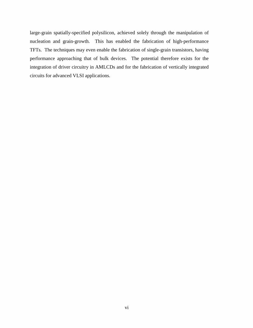
1.2.2: Vertical integration of active devices
Provided it is possible to fabricate high-performance TFTs, another important
application of TFTs emerges - vertical integration of active devices for VLSI
applications. Increasing chip area and decreasing feature size have resulted in
interconnect delay becoming a significant fraction of the overall chip delay. Numerous
techniques are under consideration to decrease interconnect delay, including the use of
low resistivity interconnect materials [17], low-k dielectrics [18], and increased packing

7
density using various techniques to increase the level of achievable integration for a
given device generation. Of these, the increase of packing density using vertical
integration of devices is particularly interesting, as it offers the additional benefits of
decreasing block-level routing complexity (through the ability to layer blocks) and
dramatically decreasing the consumed silicon real-estate. Various simple vertically
integrated cells have been demonstrated in the past, such as vertically integrated SRAM
cells [19]. A typical vertically-integrated inverter cell is shown below (Figure 1.7).
Conventional 2-D integration: low packing TFT-based 3-D integration: high packingdensity density
Figure 1.7: Standard and vertically integrated inverter cells
Vertical integration of devices using thin film transistors is a promising means of
achieving 3-D integration. Unfortunately, TFT performance is typically substantially
worse than that of bulk devices, limiting the use of such cells to non-critical paths only.
Additionally, for deep sub-micron VLSI applications, statistical variation in device
performance is introduced by the random distribution of grains in the device [20], since
the grain size is on the order of the device size. This variation in performance results in
unacceptably poor uniformity. Uniformity can be improved by reducing the grain size;
however, this degrades device performance substantially. These are important issues that
will be discussed in some detail in a later chapter. However, provided it is possible to
solve these problems, vertical integration of active devices using TFTs should enable a
substantial improvement in circuit performance through a reduction in interconnect delay.
Figure 1.8 illustrates this reduction in interconnect length through vertical integration.
8
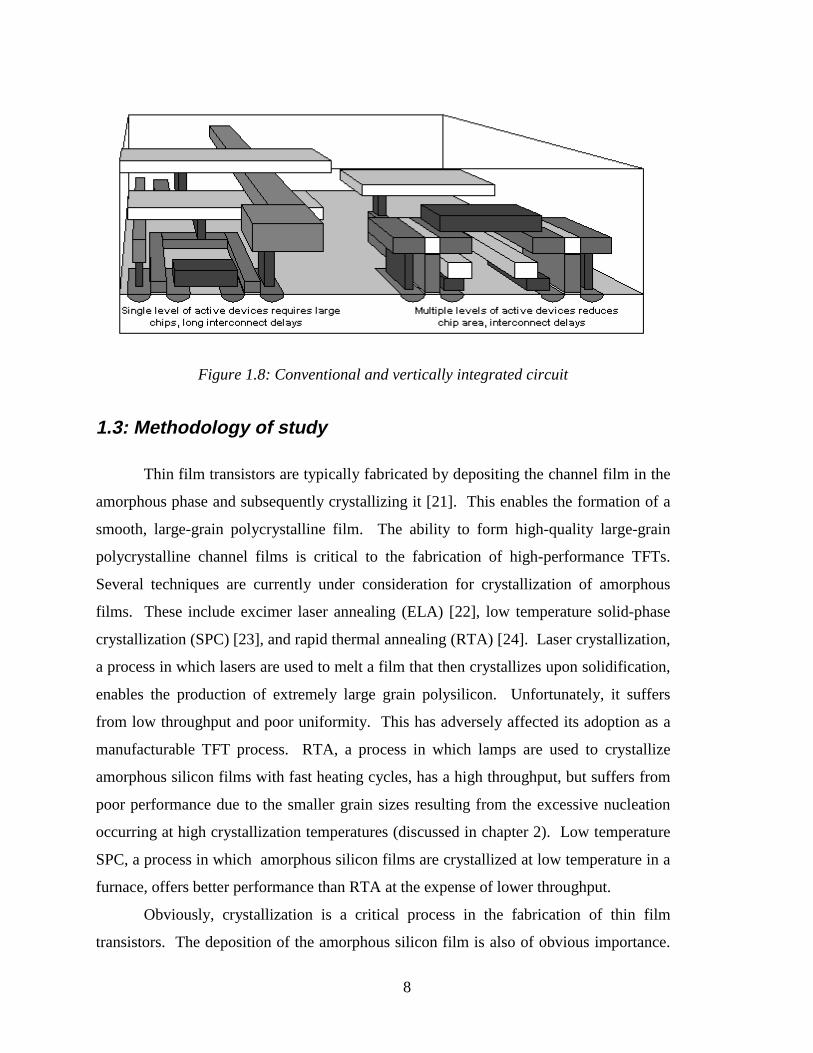
Figure 1.8: Conventional and vertically integrated circuit
1.3: Methodology of study
Thin film transistors are typically fabricated by depositing the channel film in the
amorphous phase and subsequently crystallizing it [21]. This enables the formation of a
smooth, large-grain polycrystalline film. The ability to form high-quality large-grain
polycrystalline channel films is critical to the fabrication of high-performance TFTs.
Several techniques are currently under consideration for crystallization of amorphous
films. These include excimer laser annealing (ELA) [22], low temperature solid-phase
crystallization (SPC) [23], and rapid thermal annealing (RTA) [24]. Laser crystallization,
a process in which lasers are used to melt a film that then crystallizes upon solidification,
enables the production of extremely large grain polysilicon. Unfortunately, it suffers
from low throughput and poor uniformity. This has adversely affected its adoption as a
manufacturable TFT process. RTA, a process in which lamps are used to crystallize
amorphous silicon films with fast heating cycles, has a high throughput, but suffers from
poor performance due to the smaller grain sizes resulting from the excessive nucleation
occurring at high crystallization temperatures (discussed in chapter 2). Low temperature
SPC, a process in which amorphous silicon films are crystallized at low temperature in a
furnace, offers better performance than RTA at the expense of lower throughput.
Obviously, crystallization is a critical process in the fabrication of thin film
transistors. The deposition of the amorphous silicon film is also of obvious importance.

9
The potential therefore exists for the manipulation of these processes to achieve high-
performance in TFTs without having to resort to non-manufacturable processes. This is
the fundamental motivation for this work. As shall be shown in chapter 2, crystallization
occurs through two phenomena - nucleation and grain growth. Potentially, these
phenomena may be manipulated to form large grain polysilicon. In particular, they may
be manipulated spatially to achieve controlled growth of grains. This opens up a host of
possibilities, including that of the formation of single-grain devices having performance
nearing that of bulk devices. The key, therefore, is to thoroughly study solid phase
crystallization of silicon and exploit the crystallization processes to form high-
performance devices. This, in fact, is the thesis of this entire work.
1.4: Organization
Chapter 2 provides the theoretical basis for this work. The chemical vapor
deposition and solid phase crystallization of amorphous silicon are theoretically analyzed
to provide a conceptual basis for the rest of this work. In particular, the concepts of
nucleation and grain growth are discussed in some detail. The kinetics of crystallization
processes are studied using atomistic models of nucleation and growth. These models are
used to develop a complete model of solid phase crystallization. This is combined with a
comprehensive model of deposition to obtain a unified model of deposition and
subsequent solid-phase crystallization. Defect formation mechanisms within solid-phase
crystallized silicon are also discussed.
Having developed a theory of crystallization in chapter 2, chapter 3 proceeds to
demonstrate a novel sensor for the detection of these processes. An acoustic temperature
and crystallinity sensor is demonstrated and characterized. Potential applications for the
sensor are also discussed.
Using the sensor developed in chapter 3, a two-step crystallization process for the
improvement of process throughput is demonstrated in chapter 4. This forms a simple
proof of concept of the possibilities for exploiting nucleation and grain growth processes
to achieve high-performance devices. A two-step crystallization anneal is used to
substantially improve process throughput while simultaneously improving device

10
performance. This is achieved through the control of nucleation and grain growth to
maximize grain size while minimizing the incubation time during crystallization.
The process used in chapter 4 does not control the spatial occurrence of
nucleation. Therefore, there is no possibility of achieving control of the location of
grains. In chapter 5, this next logical step is taken. Using a similar two-step
crystallization process, spatial control is achieved by a technique called lateral
crystallization using patterned light absorption masks. Selective heating is used to
spatially control the occurrence of nucleation and hence achieve control of grain location.
This enables the fabrication of extremely high-performance devices. By this means, the
conceptual basis for lateral crystallization is introduced. The use of such processes to
tune device performance for its intended application is discussed.
Chapters 3 through 5 all demonstrate the control of nucleation and grain growth
during the crystallization process. In chapter 6, the same effect is achieved through
control of the deposition conditions for the amorphous film. The deposition conditions
are optimized to maximize grain size and fabricate high-performance devices. Atomistic
models of deposition are used to explain the experimental results and a comprehensive
model of optimization and optimization extents is developed. This is performed for the
silicon-germanium system, since it is an extremely promising system for the fabrication
of low thermal budget TFTs, and enables the demonstration of key surface attachment
concepts.
In chapter 7, some of the properties of the silicon-germanium system are
exploited to demonstrate another new type of lateral crystallization - germanium-seeded
lateral crystallization. Using this technology, nucleation is selectively induced to form
large grain spatially specified polysilicon. Devices having extremely high-performance
approaching that of bulk devices are fabricated, potentially suitable for use in the vertical
integration of active devices for VLSI applications.
Finally, in chapter 8, the contributions of this work are summarized and possible
further areas of investigation are discussed.

11
Chapter 2
The Chemical Vapor Deposition and Solid-Phase
Crystallization of Amorphous Silicon
___________________________________________
The deposition of silicon from a gaseous source is one of the most important
processes in modern microelectronics. Chemical vapor deposition is used in epitaxy,
deposition of polycrystalline silicon, and deposition of amorphous silicon. Epitaxial
layers are used in modern bipolar technologies to form buried doped layers [1], and are
also gaining use in advanced isolation [2] and source / drain engineering processes [3] for
CMOS. Polycrystalline silicon has traditionally been used as a gate electrode for MOS
devices [4], and is also used as an emitter contact in some bipolar technologies [5].
Amorphous silicon is used as an active layer in thin film transistors (TFTs) for flat panel
display applications [6] and in solar cells [7]. Thus, a proper physically based
understanding of the deposition of silicon is critical to advancement of numerous
microelectronics processes.
Various techniques exist for the deposition of silicon, including low-pressure
chemical vapor deposition (LPCVD), plasma-enhanced chemical vapor deposition
(PECVD), metallo-organic chemical vapor deposition (MOCVD), and ultra-high vacuum
chemical vapor deposition (UHVCVD). Of these, low-pressure chemical vapor
deposition is the dominant technology in microelectronics, particularly for the deposition
of amorphous and polycrystalline silicon. LPCVD offers several advantages over other
deposition technologies, including simplicity of technology, easy scalability to large
volumes and batch sizes, and good film characteristics. Additionally, a large and fairly
cohesive body of work studying and modeling the LPCVD of silicon exists. In this work,
the deposition of silicon by LPCVD is studied exclusively.
In recent years, the crystallization of amorphous silicon films has become a
technologically important process. Crystallized amorphous silicon films are used in

12
polysilicon TFTs [8] for active matrix liquid crystal display (AMLCD) applications.
Crystallized amorphous silicon is also seeing increased use as a gate material in
MOSFET technologies, due to its smooth surface relative to as-deposited polysilicon [9].
Various techniques to crystallize amorphous silicon exist, including low-temperature
solid phase crystallization (LT-SPC) [10], rapid thermal annealing (RTA) [11], and
excimer laser annealing (ELA) [12]. Each has its own advantages and disadvantages.
ELA results in extremely large grain polysilicon with a low defect density. However, it
is an extremely slow, inherently serial process, and also has poor uniformity. RTA has a
very high throughput, but results in the formation of small-grain polysilicon. LT-SPC
offers performance between that of RTA and ELA, but is an extremely slow process.
However, it is well suited for batch processing, and this somewhat mitigates the slow
process throughput. In this work, thermal solid-phase crystallization techniques (LT-SPC
and RTA) are used exclusively. Provided certain problems are solved relating to these
processes, their long-term promise is excellent relative to ELA.
In this chapter, the physics of the low-pressure chemical vapor deposition and
solid phase crystallization of amorphous silicon are discussed. Atomistic models are
used to enable an intuitive understanding of the deposition and crystallization processes.
Models of the deposition and crystallization are developed, and these are used to identify
important phenomena affecting the characteristics of crystallized silicon films. The
implications of these phenomena on thin film transistor device technologies are
discussed, with several important conclusions being introduced. These form the basis for
the experimental work detailed in subsequent chapters.
2.1: Low-pressure chemical vapor deposition of silicon films
LPCVD of silicon is achieved using a variety of source gases. The various
hydrides and halides of silicon are the most common, including silane (SiH4),
dichlorosilane (SiH2Cl2) and disilane (Si2H6). Of these, silane is definitely the most
widely used. The importance of disilane is rapidly increasing for the deposition of
amorphous silicon, for reasons that will be discussed in a later chapter. However, the
silane-based deposition of silicon has the best-understood chemistry. The analysis of this
system is considerably simpler than the analysis of halide-based deposition. For this
13
reason, in this work, to develop an intuitive, physically-based model of Si deposition, the
silane-based deposition of silicon is considered exclusively.
2.1.1: Process chemistry
The deposition of silicon from silane is thought to occur through several
intermediate reactions [13]. The silane molecule dissociates into several different silicon
hydrides. To simplify analysis, it is convenient to assume that one of the reactions is
dominant, and ignore all the other hydrides. In this work, as in other works on the subject
[14], it shall be assumed that SiH2 is the primary intermediate silicon hydride involved in
the main chemical pathway. The overall process proceeds as follows:
In the gas-phase, the silane dissociates [15]:
224
1
1
HSiHSiHk
k
+←→
−
Equation 2-1
where:
k1 and k-1 are the forward and backward reaction rate constants respectively
The SiH2 then physisorbs to the substrate. Here, it may undergo surface diffusion,
evaporation, or chemisorption to an adsorption site. The chemisorption reaction is:
22 **2
2
SiHSiHk
k
⋅←→
+−
Equation 2-2
where:
* is the adsorption site
k2 and k-2 are the forward and backward reaction rate constants respectively
The adsorbed species then releases the hydrogen to form a new adsorption site.
This process may occur after a substantial delay, depending on the temperature, etc [16].

14
↑+⋅→⋅ 23
2 ** HSiSiH k
Equation 2-3
where:
*⋅Si is a new adsorption site, one monolayer higher
k3 is the forward reaction rate constant
The adsorption site may be a on growing step (true in epitaxy) or may be on a flat
surface (true in the deposition of amorphous silicon). In the deposition of polysilicon,
both site reactions are expected to occur. The process is shown schematically below.
Locally organizedentity formed bydiffusing species
Desorbing Species
Adsorbing Species
Surface DiffusingSpeciesBuried atom
(no organization)
Figure 2.1: Schematic view of silicon deposition process
In general, the silane decomposition (Equation 2-1) is expected to occur readily in
the gas phase at typical Si deposition temperatures (>500°C). Therefore, the surface
reactions are the rate-limiting steps. Prior to proceeding with a detailed analysis of the
deposition reaction rates, an atomistic understanding of the adsorption / desorption
processes is useful. As shall be shown later, these processes critically determine the
quality of the amorphous precursor film and therefore the quality of the crystallized
silicon film.

15
2.1.2: Adsorption processes
The two-stage adsorption reaction of the reacting silicon hydrides on the growing
substrate surface is easily illustrated in an energy-position diagram [17], shown below:
Distance Coordinate
Po
ten
tial
En
erg
y0
A
B
CD
G
E
F
qpEp
Figure 2.2: Potential energy vs. distance from adsorption site for silicon deposition
where:
Chemisorption is ABC
Physisorption is DEF
The precursor state is E
The final state is B
After physisorption, several processes may occur prior to chemisorption:
1. The adsorbate may desorb off the surface.
2. The adsorbate may diffuse along the surface to a different site
3. The adsorbate may stay at the current site till it is chemisorbed
The diffusion along the surface is the critical reaction affecting the final
characteristics of the deposited film. This process determines the amount of organization
at the growing interface, directly determining whether the deposited film is
(poly)crystalline or amorphous.

16
If the area concentration of surface sites per unit time is Ns and the deposition flux
is J, then the lifetime on the surface prior to adsorption is (assuming the species does not
desorb):
J
Nt s
L =
Equation 2-4
where:
tL is the diffusion lifetime on the surface
Ns is the adsorption site surface density per unit time
J is the deposition flux
If the assumption that the lifetime of the adatom prior to desorption is much
greater than tL is maintained, then the mean diffusion distance before being buried is:
( )2
1
4 LsBS tDX =
Equation 2-5
where:
Ds is the surface diffusion coefficient
tL is the diffusion lifetime
XSB is the mean diffusion distance
Now, from this equation, it is possible to predict regimes during which a
deposited film will be (poly)crystalline or amorphous. If the diffusion distance is
substantially less than the distance between adsorption sites, then there will be little
organization on the surface by adatoms prior to being buried. This will result in an
amorphous film. If, on the other hand, the adatoms have sufficient time to organize on
the surface prior to sticking, then the resulting film will be (poly)crystalline.

17
Mathematically:
Amorphous Deposition: 24 s
sN
JD ≤
Equation 2-6
Polycrystalline Deposition: 24 s
sN
JD >>
Equation 2-7
In fact, the less the organization, the more “amorphous” the film. Thus, the above
relationships can be used to establish a quality factor for amorphous films. To relate the
above equations to deposition temperature and pressure, the flux and diffusivity are
rewritten as [18]:
Tm
PJ
κπ2=
Equation 2-8
where:
P is the partial pressure of the impinging species
m is the mass of the impinging species
κ is Boltzmann’s constant
−=
T
EDD A
Si κθ exp0
Equation 2-9
where:
D0 is a pre-exponential term
EA is an activation energy
θ is the fraction of open surface sites

18
Additionally, to incorporate the energetics of the bonding process itself, a reaction
rate term must be added to account for the chemical bonding reaction and hydrogen
desorption reactions. This can be achieved by including an additional energy activation
term. Thus, a “quality factor” can be established, relating the deposition conditions to the
quality of the amorphous film.
+−
==
T
EEDNTm
P
ND
JQ
RAs
sSi
κθκπ exp2 0
22
Equation 2-10
where:
ER is an activation energy accounting for the various reaction processes.
The quality or “amorphousness” of the film increases as Q increases. Several
conclusions can be drawn from this equation:
1. The film becomes more amorphous as the pressure increases
2. The film becomes more amorphous over large temperature decreases
3. The effect of small temperature decreases depends on the various pre-exponential and
linear parameters
The above conclusions are generally valid. However, it should be noted that the
surface conditions are not constant throughout growth. In particular, growth
characteristics are different for the first few monolayers of deposition, when the substrate
(SiO2 is used exclusively in this work) has not been fully covered with a stable film. An
analysis of this growth regime is therefore important, as it will affect the growth of
subsequent layers, and will also affect solid-phase crystallization, as shall be seen later.
2.1.3: Initial nucleation on amorphous substrates
The deposition of silicon on amorphous substrates, specifically on SiO2, proceeds
as a net result of adsorption and desorption of silicon-containing species from the gas-
phase. To simplify analysis, the following assumptions are useful:

19
1. The adsorbent surface is planar and the total number of adsorption sites is constant
under all experimental conditions.
2. The adsorption is restricted to a monolayer.
3. On impact with a free site, the adsorbate is adsorbed with zero activation energy.
4. An occupied site comprises one adsorbed molecule at a single site.
5. Collisions of gaseous molecules with an adsorbed site are perfectly elastic.
6. Desorption of an adsorbed molecule occurs as soon as it has acquired sufficient
thermal energy to equal the heat of adsorption.
7. The adsorptive properties of all surface sites are identical.
8. There are no lateral interactions between neighboring adsorbed molecules.
The above assumptions in fact define a Langmuir adsorption isotherm [17]. The
adsorption and desorption rates are:
)( ssa
a
s nNPkdt
dn−=
Equation 2-11
sd
d
s nkdt
dn=
Equation 2-12
where:
ns is the concentration of adsorbates on the surface
ka is the adsorption rate constant per site at unit pressure
kd is the desorption rate constant per site
From these equations, the time dependence of adlayer build-up is established:
sadsas nPkkPNk
dt
dn)( +−=
Equation 2-13

20
If the assumption is made that kaPNs and kd + kaP are constant, i.e., the adsorption
and desorption are time-independent, then the solution is:
[ ]{ }tPkkPkk
PNktn ad
ad
sas )(exp1
)()( +−−
+=
Equation 2-14
In real semiconductor systems, at least some modifications to the results of the
simple assumptions above are expected, including:
1. kd/ka will be a function of ns because of surface relaxation and reconstruction.
2. There will be additional losses from the pool of monomer adspecies due to dimer,
trimer, etc. species formation plus losses by diffusion to any nearby ledges.
These result in:
[ ]{ } ∑∞
=
−⋅+−=
211
1 )(m
smsssa
s
dt
mdnnPnKPNk
dt
dn
Equation 2-15
where the various ns terms account for higher order effects
For many semiconductor systems, it has been found that the K(ns1) term is
dominant. Tiller [17] performed an analysis of a single-component surface species by
making the assumption that the gas atoms adsorbed on the surface behave as a two-
dimensional gas with a spreading pressure ϕ. This results in the analogue of a van der
Waals’ equation of state in two dimensions:
b
T
b
a θκθθϕ =−
′
+ )1(22
Equation 2-16
where
A
bn′=θ , is the surface coverage
Equation 2-17

21
A is the substrate area
n’ is the number of adsorbed atoms
b is the area per adsorbed atom
a’ is related to the molecule-molecule binding energy in the adlayer
Using the Gibbs adsorption equation
b
T
A
nT
Pd
d θκκϕ −=′
−=ln
Equation 2-18
results in
)exp()1
exp(1 12*
θθ
θθ
θKK
P
P −−
−=
Equation 2-19
where
Tb
aK
κ′
= 21
Equation 2-20
is the adatom-adatom binding energy
K2-1 is proportional to the adatom-substrate binding energy
P* is the equilibrium vapor pressure of the adsorbed substance.
Based on the above equation, the following regimes of growth can be defined:
1. K2-1 >> K1 - desorption energy is high compared to heat of sublimation, resulting in
layer-by-layer growth
2. K1 ≅ K2-1 - classical nucleation regime; coverage is less than one monolayer
3. K2-1 << K1 - very low desorption energy compared to heat of sublimation resulting in
very low surface coverage; very high supersaturation is required to produce
heterogeneous nucleation via very small clusters.

22
The above regimes have important implications on the solid-phase crystallization
of amorphous silicon. If the initial sticking to the surface is poor, then layer-by-layer
growth may result initially. The net result of this is the formation of locally organized
entities in the first few monolayers of deposited film, which act as crystallization sites
during solid-phase crystallization processes. In fact, as shall be shown later, most SPC
experiments result in crystallization starting at the bottom interface of the film; this is a
direct consequence of the initial local organization.
To appreciate the physical basis for the difference in the deposition conditions
affecting the first few monolayers and those affecting all subsequent layers, it is
necessary to proceed with an analysis of the deposition process and chemistry.
2.1.4: Deposition process
The deposition of silicon, as stated earlier, occurs through a series of
decomposition, adsorption, and desorption reactions. Experimentally, the deposition of
silicon has been found to occur in two regimes:
1. Diffusion limited regime - growth is limited by reactant supply from the gas-phase
2. Surface controlled regime - growth is limited by reaction at the growing interface
In addition, the surface controlled regime has been found to be further divided
into two regimes depending on the level of surface hydrogen present:
1. Hydrogenated surface layer present - growth is strongly limited by the desorption of
hydrogen from the surface to form a new adsorption site.
2. Hydrogenated surface layer absent - growth is limited by adsorption reaction.
These regimes of deposition have been demonstrated experimentally. Depending
on the regime of deposition, the growth rate has a different activation energy. Bloem and
Giling [19] summarized various results to show the regimes of deposition, shown below:
23
log
R
1/T
DiffusionLimited
SurfaceControlled
HydrogenatedSurface Layer
Absent
Present
~210 kJ / mole
~140 kJ / mole
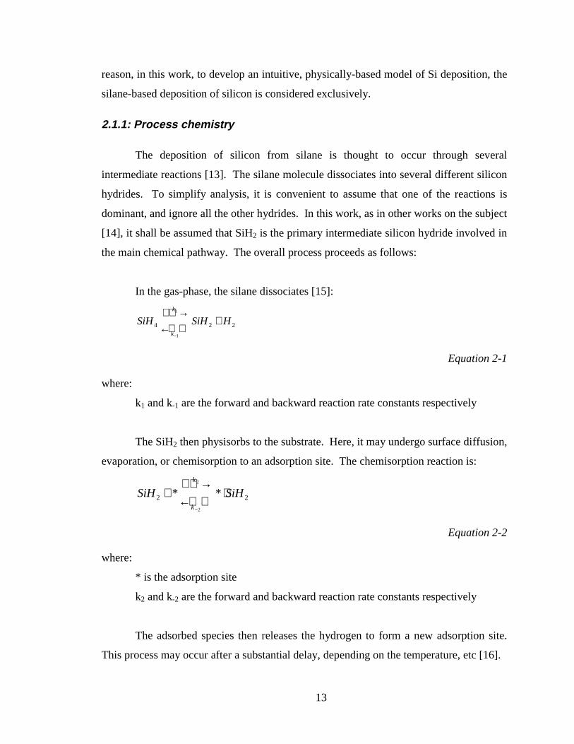
Figure 2.3: Growth rate of silicon as a function of temperature
The change in activation energy between the two surface-controlled regimes is
accompanied by a change in emissivity. There is a surplus emissivity for the hydrogen-
desorption limited regime. This has been explained as being caused by the presence of a
hydrogen-terminated surface [19]. This termination is purely kinetic in nature; as soon as
the growth stops, the excess hydrogen “boils” off. To quantify the effect of this hydrogen
on the deposition rate, the individual components of the activation energy can be
calculated using numerical values from Bloem and Giling [19]:
Activation Energies:
1. Gas-phase reaction of SiH4=SiH2+H2 ∆H1= +218kJ/mole
2. Adsorption of SiH2 on the Si surface ∆H2= -216kJ/mole
3. Formation of second Si-Si bond ∆H3= -216kJ/mole
4. Desorption of 2H from Si-H bonds ∆H4= +2 × 180kJ/mole
Total ∆Htot= +146kJ/mole
Thus, the surplus in the activation energy, calculated from the experimentally
observed activation energy (Figure 2.3) and identified as the component added by
hydrogen desorption, is approximately 60kJ/mole. In the figure above, this corresponds
24
to the difference in slopes of the deposition rate curve above and below the dashed line.
This value of desorption activation energy is in good agreement with experimental data
[20], validating the model of hydrogen-desorption limited deposition at low temperatures.
To deposit amorphous silicon by LPCVD, all depositions are performed in this regime,
and hence, in this work, all depositions are assumed to be hydrogen-desorption limited.
This assumption allows the development of a new limited model of deposition,
suitable for analysis of the effect of pressure on depositions occurring in this regime [21].
To proceed, the following assumptions are made:
1. All depositions are limited by the availability of adsorption sites on the growing
surface.
2. Adsorption site formation is limited by the desorption of hydrogen.
3. The partial pressure of hydrogen in the gas-phase is low; all produced hydrogen is
rapidly removed from near the substrate.
Through these assumptions, it is possible to model the deposition as a surface-
catalyzed process, where the open surface sites are catalysts. Since the reaction is limited
by hydrogen desorption, and the desorption is fixed for a given temperature and pressure,
it is possible to decouple the desorption process and bury the desorption coefficient in the
silicon-hydride adsorption reaction (Equation 2-2). Then, combining the two surface
reactions (Equation 2-2 and Equation 2-3), a standard Michaelis-Menten catalyzed
reaction rate equation can be developed [22]:
Pk
PEkR
M
tot
+⋅⋅= 3
Equation 2-21
where:
k3 is the rate constant from the desorption equation (Equation 2-3)
Etot is the total number of surface sites available at any given time
P is the deposition pressure (or partial pressure, if a carrier gas is used)
kM is a constant
R is the deposition rate
25
Etot is a function of the hydrogen desorption. If the hydrogen partial pressure is
low (true for typical LPCVD with no carrier gas, as used in this work), then this is
essentially independent of pressure and is purely a function of temperature. Furthermore:
2
32
k
kkkM
+= −
Equation 2-22
where:
k-2 is the reverse rate constant from the adsorption equation (Equation 2-2)
k3 is the rate constant from the desorption equation (Equation 2-3)
k2 is the forward rate constant from the adsorption equation (Equation 2-2)
Since the hydrogen desorption is buried with k2, k2 decreases as the amount of
hydrogen desorption decreases. This in turn makes a plot of the deposition rate vs.
pressure more linear. If the hydrogen desorption is high, then the plot develops a strong
“knee”. This phenomenon becomes important in a later chapter, when the deposition of
silicon-germanium is studied.
In the deposition of amorphous silicon, the hydrogen-desorption-limited growth
has various effects:
1. The chemisorption rate is reduced as the substrate temperature is reduced, increasing
the diffusing lifetime of the physisorbed species; merely decreasing the temperature
will not improve amorphous silicon film quality ad infinitum, even though the
diffusivity decreases.
2. During the initial stages of deposition on a substrate, organization will be enhanced.
Deposition on the stable (through surface reconstruction and other phenomena)
substrate interface is slow compared to desorption. Therefore, physisorbed species
have an enhanced initial diffusing lifetime, resulting in increased initial organization.
2.1.5: Unified description of amorphous silicon deposition
Having described the various phenomena affecting the deposition of silicon, it is
possible to develop a unified description of the deposition of amorphous silicon on

26
amorphous substrates. As shall be shown later, the effect of the amorphous silicon on the
final characteristics of the SPC polysilicon is substantial; therefore, such a unified
description of deposition is crucial to optimizing the characteristics of the final
crystallized film.
Amorphous silicon deposition on an amorphous substrate, by definition, does not
proceed through a step-based growth mechanism such as that which occurs during silicon
homoepitaxy [19]. Therefore, the growth occurs through a process of nucleation, growth,
and coalescence. The critical process affecting the quality of the amorphous silicon is
nucleation.
Nucleation (and growth in general) occurs through a process of physisorption of a
mobile silicon-hydride species. This species then diffuses on the surface and may
subsequently desorb or stick. The extent of diffusion determines the level of organization
achieved in the growing film prior to the atom in question being buried. To achieve a
more amorphous film, the amount of organization occurring must be reduced. This can
be done in various ways:
1. The surface diffusivity may be reduced by reducing the substrate temperature.
2. The lifetime on the surface may be reduced by increasing the arriving flux, hastening
the burial of the diffusing species.
3. The chemisorption rate may be increased by increasing the concentration of
adsorption sites through increased hydrogen desorption.
The net result of any or all of these modifications is a reduction in the amount of
organization occurring at the growing film surface, increasing the amorphous quality of
the final film. As shall be shown, this is critical to obtaining large-grain solid-phase
crystallized silicon films.
Having established the various stages of deposition and the effects of the same on
the characteristics of the deposited film, it is possible to summarily describe the structure
of a typical amorphous silicon film deposited by LPCVD. Consider the deposition of
such a film onto an amorphous substrate such as silicon dioxide. During the initial stages
of growth (first few monolayers), the substrate surface is not fully covered. Since the
substrate surface is passivated due to surface reconstruction, the initial density of

27
chemisorption sites is low and deposition proceeds slowly. Additionally, slower
deposition occurs for another technological reason. In a typical hot-wall reactor, when
the source gas is first turned on, its partial pressure is low as it takes a finite amount of
time for the source gas to replace the inert carrier gas initially in the reactor. During this
time, deposition is slow, since the flux, which is proportional to the source gas partial
pressure, is reduced. For these two reasons, for the initial few monolayers, the amount of
local organization occurring is high, and the deposited film is “less” amorphous.
After the substrate surface is fully covered and the gas pressure has stabilized, the
growth proceeds normally, resulting in a “more” amorphous film. At the end of the
deposition step, the source gas flow is cut off, and again the partial pressure drops in a
finite time, resulting in slower deposition, though this is less significant than during the
initial stage of deposition, since reduced adsorption site concentration due to surface
reconstruction is not a significant issue. Since hydrogen desorption is the deposition
limiting step anyway, gas-phase supply is less of an issue than any surface effects
anyway. The overall deposition results in the film structure shown below (Figure 2.4).
Substrate (Oxide)
Amorphous film
Substrate
Increased diffusion dueto stable surface
LessFlux
Initial Stage
Film
LessFlux
Final Stage
Film
Normal
Substrate
Locally organizedcrystallites
Figure 2.4: Structure of deposited film
The film structure has several important implications for solid-phase
crystallization processes, as will be discussed later in this chapter.

28
2.2: Solid-phase crystallization of amorphous silicon
Having discussed the deposition of amorphous silicon from a gaseous source, it is
now possible to develop a model of solid phase crystallization of this deposited film,
accounting for the variation in the “amorphousness” of the film itself. To do this, the
model shall be developed in two stages:
1. A model of crystallization shall be developed assuming basic transient nucleation
theory, ignoring the effect of pre-existing organized sites.
2. The effect of pre-existing organized sites on the grain density shall be analyzed.
To begin, a conventional thermodynamic model of nucleation and growth shall be
specified based on atomistic considerations.
2.2.1: Thermodynamic considerations of nucleation and growth
From classical nucleation theory, modified to include transient nucleation theory
in condensed systems [23], the initiation of a phase transformation occurs through
frequent nucleation of microcrystallites. Most of these microcrystallites are energetically
unstable and therefore shrink and annihilate due to their large surface-to-volume ratio.
However, from statistical thermodynamic considerations, a few microcrystallites become
large enough to achieve stability due to the reduction in free energy associated with the
increase in size. In general, the free energy of formation of a cluster of n atoms or
molecules is given by:
σnn AGnG +′∆=∆
Equation 2-23
where ∆G’ is the difference in the Gibbs free energies between the new and old
phases, per molecule (hence, it is negative)
An is the surface area of the cluster of n atoms
σ is the interfacial free energy per unit area (positive).

29
Equation 2-23 indicates that the free energy of a cluster increases to a maximum
value as the size of the cluster is increased, and then reduces. This cluster size is in
unstable equilibrium; smaller clusters (or embryos) tend to shrink and larger clusters (or
nuclei) tend to grow.
Classical theory suggests that there is no back flow in reaction; that is, nuclei (as
opposed to embryos) are not annihilated. In fact, this intuitively and physically makes
little sense. Transient nucleation theory corrects for this by introducing a forward and
backward reaction rate for critical and super-critical crystallites as well. In general, since
the growth process occurs through atomic hops, it is possible to develop an atomic model
of the reaction process.
The unbiased atomic jump rate (in amorphous silicon, since the jump is from the
amorphous to the crystalline phase) is given by [24]:
−∝
kT
Edexpν
Equation 2-24
where Ed is the activation energy of self-diffusion in amorphous silicon.
Now, in a system where the free energy of the cluster of n+1 atoms exceeds that
of a cluster of n atoms, the biased atomic jump rates for the forward and backward
reactions are [24]:
( )
∆−∆
−
∝ ++→ kT
GG
kT
Enk nnd
nn 2expexp 13
2
1
Equation 2-25
( )
∆−∆
−
∝ +→+ kT
GG
kT
Enk nnd
nn 2expexp 13
2
1
Equation 2-26
where n is the number of atoms in the cluster.
30
Using these reaction rates, it is possible to determine thermodynamic
characteristics of solid-phase crystallization, including transient time, nucleation rate, and
growth velocity.
Transient nucleation time and steady state nucleation
Transient nucleation time is the time taken for the nucleation rate to achieve its
steady-state value. Several authors have studied transient nucleation in varying degrees
of detail [23, 25]. In general, numerical solutions have been found to provide the most
precise answer. However, for our purpose, an approximate answer after Kashchiev [25]
will suffice.
In general, transient nucleation has been found to be associated with a
characteristic time, having a weak temperature dependence:
*n
t k
T∝τ
Equation 2-27
where:
τt is the characteristic time
k*n is the forward or reverse reaction rate at the critical cluster size
The transient nucleation time has been found to be proportional to τt:
∝
kT
ET dexp0τ
Equation 2-28
where:
τ0 is the transient nucleation time
Ed is an empirical activation energy
While this is not a true Arrhenious form, it is apparent that the transient time
increases as the temperature is decreased. Here, we make the simplifying assumption

31
that the nucleation is negligible before a specific time and then rises rapidly to its steady
state value. This time is commonly described as the “incubation time”, and increases
with decreasing temperature. This will have important consequences when the concept
of lateral crystallization is introduced in chapter 5. In that chapter, crystallization is
performed at a very low temperature to maximize the incubation time within practical
limits.
Kelton [23] performed a detailed numerical simulation of transient nucleation to
obtain the theoretical temperature dependence of steady state nucleation as:
( )
∆+−∝
kT
GETr nd
n
*
exp)/1(
Equation 2-29
where rn is the steady-state nucleation rate
Based on Kelton’s simulations, various conclusions can be drawn:
1. The simple form of the transient nucleation time equation (Equation 2-28) is
generally valid, i.e., incubation time increases with decreasing temperature in a
roughly Arrhenious manner.
2. The critical cluster size is itself a function of temperature and increases with
increasing temperature, resulting in a decrease in the nucleation rate at high
temperatures.
3. Addition of a pre-existing embryo and nucleus population increases the amount of
nucleation.
These three phenomena have important consequences:
1. To minimize nucleation and maximize the incubation time, crystallization should be
done at as low a temperature as practical.
2. Pre-existing organized entities must be minimized to minimize nucleation.
3. Ideally, crystallization should be done at an extremely high temperature with an
instantaneous ramp-up. This results in a low nucleation rate due to the large critical
cluster size, accompanied by a high growth rate, as will be shown below. In practice,
32
however, this is impossible, since several nuclei form and grow during the ramp
process.
Figure 2.5 shows the various regimes of nucleation as a function of crystallization
temperature.
log
rn (
cm-3
sec
-1)
1/T
Critical ClusterSize Limited
Atomic HopLimited
RoughlyArrheniousBehavior
ExperimentallyObservable Regime
Figure 2.5: Regimes of nucleation during solid-phase crystallization
Growth rate
The growth rate is the enlargement rate for existing grains and can be calculated
from the net forward reaction rate for a large cluster. For such a cluster, the addition of
an atom will not substantially alter the surface energy. The free energy change is then -
∆G’. From the attachment equations (Equation 2-25 and Equation 2-26), by assuming
∆G’ >> 2kT, we have:
nnnn kkdt
dn→++→ −= 11
Equation 2-30
′∆−−
′∆
−∝
kT
G
kT
G
kT
En
dt
dn d
2exp
2exp
)exp3
2
Equation 2-31

33
′∆−−∝
kT
GE
ndt
dn d 2exp3
2
Equation 2-32
Since n is proportional to the cube of the radius of the growing phase:
′∆−−∝=
kT
GE
dt
drv
d
g2exp
Equation 2-33
Where vg is the phase growth rate
Clearly, the growth rate exhibits an Arrhenious dependence. Prior to proceeding
with our model development, it is appropriate to survey the literature values of the
Arrhenious coefficients. The sources used are Iverson and Reif [24], Zellama et al [26],
Koster [27], Blum and Feldman [28], and Csepregi [29].
Table 2-1: Survey of crystallization activation energies.
Work Transient Time Nucleation Rate CharacteristicCrystallizationTime
Growth Rate
Iverson & Reif 2.7eV1 5.1eV2 3.9eV 3.3eVZellama et al 4.9eV3 2.4-4.9eVKoster 4.9eV 2.9eVBlum & Feldman 3.1eVCsepregi 2.35eV4
1 This results in a self-diffusion activation energy of 2.8eV2 Maximum free energy of formation of a cluster, ∆Gn
* is 2.4eV3 Reports a high activation energy of 9eV for films deposited at room temperature, probably caused by the fact thattransient nucleation was not considered. For room temperature depositions, density of pre-existing nuclei isexpected to be low, resulting in a longer transient time.4 For <111> epitaxial regrowth
Various conclusions can be drawn from the above data:
34
1. The activation energy of growth is less than the activation energy of nucleation.
Therefore, nucleation can be minimized relative to growth by performing the
crystallization at the lowest practical temperature.
2. Transient time activation energy is significant compared to the nucleation activation
energy and therefore cannot be ignored.
3. In general, the agreement between the various sources is fairly good. Any
discrepancies can be explained by the theory established here.
Crystalline fraction
The rate of nucleation per unit amorphous area is ∈rn, where ∈ is the film
thickness. If the nucleation and growth rates are time-independent (true after transient
time), then the crystalline fraction is:
( )
−−−=
3
30exp1)(
c
tt
ττχ
Equation 2-34
where τc is the characteristic crystallization time:
3
1
2
3
−
∈
= ngc rv
πτ
Equation 2-35
This is a form of the Avrami-Johnson-Mehl equation [30, 31, 32].
Grain density
Since the nucleation rate is proportional to the amorphous fraction and to the 2-D
nucleation rate, the density of grains can be written as:
[ ] tdtrtt
nG ′⋅′−∈= ∫0
)(1)(τ
χρ
Equation 2-36

35
∫ ′′−=∈u
cnG udurt0
3 )exp()( τρ
Equation 2-37
Final grain size
The final grain size can be calculated as:
[ ] 1)(lim −
∞→= t
tA GG ρ
Equation 2-38
3
23
1
3
43
∈
Γ
=n
gG r
vA
π
Equation 2-39
where Γ is Euler’s gamma function
This gives an extrapolated final grain diameter of:
GG Ad
=π4
Equation 2-40
Equation 2-39 provides us with a quantitative relationship between grain size,
nucleation, and grain growth. From this equation, it is apparent that the intuitive
argument that grain growth can be maximized by minimizing nucleation relative to grain
growth is correct.
Having established the temperature dependencies of nucleation and grain-growth,
it is appropriate to compare the same to obtain an intuitive understanding of the
crystallization process. From the summary of literature data (Table 2-1), it is apparent
that the activation energy of nucleation is greater than that of grain growth. Thus, the
slopes of the two curves will be different. Additionally, at higher temperatures, the

36
critical cluster size of a stable nucleus is large; this becomes the limiting factor in
nucleation, and the nucleation rate decreases at elevated temperatures.
From the stated trends, it is clear that the largest grain size, resulting from the
maximum grain-growth to nucleation ratio, would occur at high temperatures (where
grain growth would be high but nucleation would be low), assuming it were possible to
reach those high temperatures instantaneously. Obviously, this is not the case, and even
rapid ramp-ups will result in substantial nucleation during the ramp process. Therefore,
from a practical standpoint, the best conditions to achieve large-grain polysilicon occur at
low temperatures, when nucleation is substantially less than grain growth. The
disadvantage of this is that both processes are slow, and therefore crystallization takes a
long time. This is an issue that will be addressed in chapter 4. Figure 2.6 shows the
tradeoffs associated with using different crystallization temperatures schematically.
log
rn (
cm-3
sec
-1)
1/T
log
vg (
cm s
ec-1
)
Ideal Regime(impossible due to finitetemperature ramp rate)
Practical Regime(disadvantage: long
anneal time)
Crystallization Goals: MinimizeNucleation Relative to Growth
Figure 2.6: Variation in nucleation and growth with crystallization temperature
Having established a basic model for crystallization, it is now possible to account
for the presence of pre-existing populations of embryos and nuclei.
2.2.2: Effect of pre-existing nuclei on grain size
Equation 2-34 describes the relationship between crystalline fraction and the
characteristic crystallization time. This time is itself a function of the growth rate and the
nucleation rate (Equation 2-35). If the presence of a pre-existing nucleus population is

37
assumed, then the effect of the same on crystalline fraction and grain density can be
analyzed in a similar fashion. First, if we assume no homogeneous nucleation, then the
crystalline fraction in the film purely from the pre-existing nuclei is:
−−=
2
exp1s
s
t
τχ
Equation 2-41
where τs is the characteristic time of crystallization in a seeded film:
sg
sv ρπ
τ2
1=
Equation 2-42
These seeded grains compete with spontaneously nucleated grains:
( )
>
−
−−−
<
−−
=
0
23
0
0
2
,exp1
,exp1
)(
τττ
τ
ττ
χ
ttt
tt
t
sn
s
Equation 2-43
where τn is the characteristic crystallization time due to nucleation.
The density of grains versus time is:
[ ]∫ ′′−∈+=t
nsg tdtrt0
)(1)(τ
χρρ
Equation 2-44
where:
∈ is the film thickness
rn is the nucleation rate, as per previous section.
From these equations, we can draw several conclusions:

38
1. The existence of a pre-existing nucleus population will tend to increase the grain
density (decreasing the average grain size) if the crystalline fraction of the film is
small or intermediate at the end of the incubation time. The reduction in grain size
will be a function of the density of pre-existing nuclei.
2. Pre-existing nucleus populations will have little effect on the average grain size if the
incubation time is small.
3. If the incubation time is large, then the pre-existing nuclei can actually enhance the
average grain size, since the pre-existing grains may actually fully crystallize the film,
in which case the average grain size will be purely a function of the pre-existing
nucleus density.
This third point is extremely important and forms the basis for several chapters in
this work. If nucleation, or a pre-existing nucleus population, can be induced into a film
with a long incubation time, then substantial grain size enhancement is possible. This is
the basis for seeded lateral crystallization, which will be discussed in detail in later
chapters.
2.3: Unification of deposition and crystallization models
At this point, it is possible to attempt an intuitive unification of the models of
deposition and crystallization to understand the effect of deposition conditions on the
structure of the final polysilicon film. The main effect of the deposition conditions is to
change the density of pre-existing nuclei within the amorphous film. Nakazawa [33]
demonstrated that the growth rate is essentially independent of deposition conditions,
though the nucleation rate shows a strong dependence on deposition temperature. This is
in agreement with the models of deposition and crystallization developed in this chapter.
Intuitively, since growth rate is purely a diffusive mechanism, it should not show any
dependence on film conditions provided the free and interfacial energies themselves
show little dependence on the amorphous matrix conditions. Nucleation rate, on the
other hand, is strongly dependent on the population of pre-existing nuclei and embryos,
and therefore shows a strong dependence on the film deposition conditions. This is
clearly visible in Nakazawa’s data, shown below (Figure 2.7)

39
0
1
2
3
4
5
420 440 460 480 500
Deposition Temperature (°C)
Nu
clea
tio
n R
ate
(x10
8 cm2 /s
eco
nd
)
0
1
2
3
4
5
Gro
wth
Rat
e (Å
/sec
ond)
Nucleation RateGrowth Rate
Figure 2.7: Temperature dependence of nucleation and growth (from Nakazawa [33])
Since the primary effect of the deposition conditions is to alter the population
distribution of pre-existing nuclei and embryos, the quality factor (Equation 2-10) may be
employed in a simple test of the efficacy of the models developed here.
Various assumptions are made:
1. A sub-set of all pre-existing nuclei grow to form grains in the final polysilicon
film (a reasonable assumption based on the analysis in previous sections).
2. Homogeneously nucleated nuclei are themselves formed from pre-existing
embryos (again, a reasonable assumption based on nucleation theory).
3. Spatial variations in embryo density (Figure 2.4) are consistent across the
deposition conditions considered here (a valid assumption if the same
substrate conditions and deposition equipment are used).
Then, the final grain size should be a pure function of the quality factor, scaled by
a linear function. This then provides a novel method for quantitatively relating the grain
size of the crystallized film to the deposition and crystallization conditions. To test this,
the model was fitted to data from Aoyama et al [34], as shown below. Clearly, the fit is
quite good, given the simplifying assumptions made. To test the physicality of the fit, the
fitting parameters can be analyzed. The linear scaling terms are largely dependent on the

40
biases introduced by the grain size estimation technique, and hence do not provide any
insight into the physicality of the fitting function. The values of interest are the predicted
activation energies associated with the exponential terms. The fitting function provides a
numerical value for the difference in the two activation energies of approximately 0.1eV.
From the work of Bloem and Giling [19], the bonding activation energy term is found to
be approximately 2.1eV. This suggests a surface diffusion activation energy of
approximately 2.0eV. Most studies of surface diffusion of silicon deal with crystalline
silicon [35, 36, 37, 38, 39, 40]. Similar studies for the diffusion of Si adsorbed species on
growing amorphous silicon surfaces do not exist. However, it is possible to extrapolate
expected values of activation energies based on those experimentally determined for
single crystal silicon. Typical values for single crystal silicon are in the range 0.6eV -
2.7eV [36, 39] depending on the direction of diffusion and substrate temperature. In
general, as the hopping distance between sites increases, the activation energy increases
above the lower limit [37]. Additionally, as the substrate temperature decreases, the
activation energy decreases below the upper limit [39]. This indicates that the value of
the activation energy of surface diffusion predicted by the fitting function is quite
realistic, attesting to the physicality of the same.
0
00
0 0
0
0
0
50
100
150
200
250
300
500 550 600Temperature (C)
Figure 2.8: Fitting of model to crystallite size data from Aoyama et al [34]

41
Aoyama’s experiments were performed using SiH4 to deposit amorphous silicon
films on glass substrates by LPCVD. His depositions were performed at 300mtorr -
1000mtorr. Thus, the range of depositions considered by Aoyama were similar to those
considered in most of this work. The analysis above suggests that, in fact, the unification
of the models of deposition and crystallization based on the alteration of pre-existing
nuclei and embryo populations provides acceptable results. Therefore, the quality factor
(Equation 2-10) may indeed be used as a means of evaluating deposition condition
viability. The various scaling factors can be determined for a given deposition system
and substrate. The substrate factors will be a function of the substrate contamination,
surface roughness, termination, etc.
Having studied the effect of deposition parameters on crystalline structure, it is
appropriate to study the effect of crystallization temperature on crystalline structure to
complete our demonstration of the efficacy of the models discussed here. In appendix 1,
the effect of defects on electron transport in polysilicon are discussed. A useful test of
the models developed here would therefore be to attempt to fit the model to experimental
electrical results obtained from TFTs.
As discussed in appendix 1, the field-effect mobility of TFTs is a function of the
trap density within the TFT channel. These may be inter-grain traps (grain boundaries)
or intra-grain traps (discussed below). If we assume that grain boundaries dominate, then
it is possible to relate grain size to crystallization parameters. To achieve this, however,
it is necessary to ensure that the crystallization processes do not affect all other factors
(intra-grain defects, grain boundary trapping behavior, etc.). This can be experimentally
accomplished by subjecting the crystallized films to a post-crystallization high-
temperature anneal. The anneal temperature can be chosen to anneal out any differences
in intra-grain defects resulting from the different crystallization temperatures without
altering the basic grain-size distribution. Experimentally, a short anneal to 1000°C has
been found to suffice. The device mobility can be correlated to crystallization parameters
as follows:
The mobility of a grain is a combination of the mobility of the grain itself and the
mobility of the grain boundaries:
42
GBGG µµµ111
0
+=
Equation 2-45
where:
µG is the mobility of the overall grain
µG0 is the intra-grain mobility
µGB is the mobility of the grain boundary
If we assume that the area of the grain boundaries parallel to the direction of
current flow is negligible (a good assumption for typical SPC films), then we can write
the overall channel film mobility as:
GB
GB
GCH
dLL
µµµ+=
0
Equation 2-46
where:
µCH is the mobility of the channel
L is the channel length
dGB is proportional to the grain boundary density
If µG is substantially more than µGB (true due to the post-anneal discussed above),
then the device mobility can be described:
GB
GBFE d
µµ ∝
Equation 2-47
where:
µFE is the device field-effect mobility

43
The proportionality (rather than an equality) is used to due to the fact that other
mobility degrading phenomena, such as scattering by interface traps, etc., have not been
considered in the above analysis.
Equation 2-47 can be written in terms of the grain area:
GGB Aµµ ∝
Equation 2-48
where:
AG is the grain area.
Equation 2-39 allows a relationship between mobility and crystallization
parameters to be established. By including the Arrhenious dependence of nucleation and
growth, we obtain:
( )
−∝
kT
EEA growthnucl
G 3
2exp
Equation 2-49
where:
Enucl is the activation energy of nucleation
Egrowth is the activation energy of grain-growth
The activation energy of nucleation can be determined by TEM or the acoustic
crystallization detection tool described in chapter 3. Experimentally, a value of 4.8eV
was determined using the acoustic crystallization detection tool. Then, the above model
was fitted to experimental results obtained from TFTs fabricated using high-temperature
post-crystallization processing to minimize other scattering mechanisms. A linear scaling
factor was used to account for these scattering phenomena. The best fit was obtained for
an activation energy differential of 1.3eV, which corresponds to a grain-growth activation
energy of 3.5eV, which is reasonably close to the values summarized from other sources
(Table 2-1). The accuracy of the fit is apparent from a plot of the theoretical and

44
experimental variations in device field-effect mobility with crystallization temperature,
shown below (Figure 2.9).
0
00
00 0
0
10
20
30
40
50
60
500 600 700 800Crystallization Temperature (C)
0 Experimental
Theory
Figure 2.9: Theoretical and experimental variation in device mobility with crystallization
temperature
At this point, it is important to consider the spatial distribution of the pre-existing
nuclei and embryo populations based on experimentally observed grain-formation
kinetics. In general, it has been observed experimentally that the majority of grains
formed in solid-phase crystallized silicon films are initiated at the bottom interface. As
mentioned previously, this is easily explained by considering the various stages of film
deposition. As shown previously (Figure 2.4), the density of pre-existing nuclei and
embryos is expected to be highest near the bottom interface. These grow to form grains
in the final polysilicon film. If the nuclei are closely spaced relative to the film thickness,
then a columnar structure results. If the spacing is larger, then three-dimensional growth
occurs initially, followed by two-dimensional growth once the top surface is reached.
Such grains may be interspersed with grains formed homogeneously within the film
itself. The general result is that most grains will be approximately as long as the film is
thick on the short axis, and may be substantially longer on the long axis (most grains in

45
solid-phase crystallized silicon films are elliptical). This is in contrast to as-deposited
polysilicon, where the film thickness usually represents the upper bound on grain
dimensions.
2.4: Defects in solid-phase crystallized polysilicon films.
At this point, it is appropriate to examine deviations from the theory discussed in
this chapter. The theory developed so far considers only one type of defect in polysilicon
- the grain boundary. Electrically, grain boundaries have a substantial impact on device
performance, as discussed in appendix 1, and hence, in this chapter, theoretical
mechanisms for reducing the grain boundary density (i.e., increasing the average grain
size) have been developed. Grain boundaries act as scattering sites and hence reduce
carrier mobility, degrading device performance [41]. Additionally, grain boundaries act
as traps, increasing device leakage [42]. For these reasons, reduction of grain boundary
density in polysilicon TFTs is extremely important.
Besides grain boundaries, another important class of defects exist - intra-grain
defects. Particularly in large-grain polysilicon, these defects may have a substantial
effect on device performance. The most important intra-grain defect in solid-phase
crystallized silicon films is the microtwin. Haji [43] et al, actually established that the
primary growth mechanism in solid-phase crystallized polysilicon is through the
formation of twin boundaries.
The formation of (111) twin boundaries permits fast propagation of the vertical
{111} planes along the [112] direction because at the twin boundary, only two atoms are
needed to form a hexar ring. Therefore, growth occurs through the formation of multiple
twins. This configuration is very favorable for the free growth perpendicular to this
direction, along [110], because from the fast growing planes, only the (110) planes are
bounded in {111} planes perpendicular to them, making them the most difficult to
extinguish. The overall growth process is shown below (Figure 2.10).
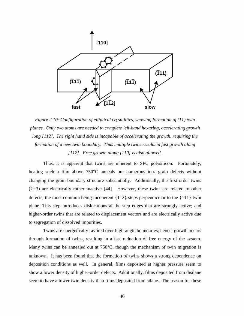
46
(111) (111)
(111)
[112]
[110]
fast slow
Figure 2.10: Configuration of elliptical crystallites, showing formation of (11) twin
planes. Only two atoms are needed to complete left-hand hexaring, accelerating growth
long [112]. The right hand side is incapable of accelerating the growth, requiring the
formation of a new twin boundary. Thus multiple twins results in fast growth along
[112]. Free growth along [110] is also allowed.
Thus, it is apparent that twins are inherent to SPC polysilicon. Fortunately,
heating such a film above 750°C anneals out numerous intra-grain defects without
changing the grain boundary structure substantially. Additionally, the first order twins
(Σ=3) are electrically rather inactive [44]. However, these twins are related to other
defects, the most common being incoherent {112} steps perpendicular to the {111} twin
plane. This step introduces dislocations at the step edges that are strongly active; and
higher-order twins that are related to displacement vectors and are electrically active due
to segregation of dissolved impurities.
Twins are energetically favored over high-angle boundaries; hence, growth occurs
through formation of twins, resulting in a fast reduction of free energy of the system.
Many twins can be annealed out at 750°C, though the mechanism of twin migration is
unknown. It has been found that the formation of twins shows a strong dependence on
deposition conditions as well. In general, films deposited at higher pressure seem to
show a lower density of higher-order defects. Additionally, films deposited from disilane
seem to have a lower twin density than films deposited from silane. The reason for these

47
phenomena is unclear; however, they may be exploited to reduce defect density within
SPC polysilicon, and, coupled with the theory developed in this chapter, may enable the
fabrication of high performance TFTs fabricated through control of the polysilicon
formation characteristics.
2.5: Conclusions
In this chapter, the theoretical basis for the low-pressure chemical vapor
deposition and subsequent solid-phase crystallization of silicon has been reviewed.
Theories developed by various other authors have been examined and have been used as
a basis to develop a unified theory of deposition and crystallization that provides a novel
means of quantifying the effect of crystallization and deposition conditions on final
crystallinity.. This theory has been used to explain experimentally-observed
crystallization phenomena, and has also been extended to explain trends seen in the
electrical performance of TFTs fabricated using different crystallization conditions. The
developed theory has been found to adequately describe the effects of deposition and
crystallization parameters on the properties of solid-phase crystallized silicon films and
TFTs fabricated from the same. Using these theories, it should be possible to optimize
the deposition and subsequent solid-phase crystallization of amorphous silicon films to
enable the fabrication of high-performance TFTs.

48
49
Chapter 3
Detection of nucleation and crystallization in
amorphous silicon
___________________________________________
In chapter 1, solid-phase crystallization and its applications to modern
microelectronics were introduced. As discussed in that chapter, solid-phase
crystallization is technologically important as a means of forming polycrystalline silicon
for the fabrication of high-performance thin film transistors. These may be used in next-
generation active matrix liquid crystal displays and, potentially, for the vertical
integration of active devices in VLSI. In both these applications, the quality of the final
polycrystalline film is extremely important. Therefore, the control of crystallization is a
crucial process for the maximization of film quality, and also for the minimization of
thermal budget to enable the integration of these devices into advanced low thermal
budget processes.
In chapter 2, the theoretical basis for crystallization was developed. As was
shown, crystallization occurs through two processes -- nucleation and grain growth. The
relative rates of these processes may potentially be controlled to maximize final film
quality. Therefore, a means of detecting nucleation and final crystallization in-situ is
highly desirable. In this chapter, a novel sensor enabling the simultaneous detection of
crystallinity and measurement of temperature during rapid thermal crystallization is
demonstrated and characterized [1]. The use of this sensor for detection of nucleation is
shown. Based on the sensor characteristics, various potential applications of the sensor to
solid-phase crystallization are discussed. These will be explored more fully in
subsequent chapters.
In this chapter, some background information on the sensor and its development
is provided. Then, the experimental methodology is explained along with details of the

50
sensor construction. Results of the sensor characterization are summarized and
implications of the same are discussed.
3.1: Background information
The sensor described in this work is an extension of a previously developed
acoustic temperature sensor [2]. This sensor has previously been used for in-situ
temperature monitoring in semiconductor processing. The sensor has been demonstrated
to function over the entire range of temperatures used in typical semiconductor
processing. It is superior to alternative temperature-sensing methods such as pyrometers.
The acoustic technique is virtually independent of the optical parameters of the sample,
enabling isolation of emissivity and surface absorption variations from the temperature
measurements. Since optical property variations due to phase transitions determine the
heating profile, the basis for the extension of the acoustic temperature sensor to
crystallinity sensing exists in systems utilizing transparent substrates.
3.1.1: Rapid thermal crystallization
Rapid thermal crystallization is a type of solid-phase crystallization. In this
process, the light from a lamp is used to heat and crystallize an amorphous silicon film on
a transparent substrate [3]. The process is promising, since it is possible to produce high-
performance TFTs without sacrificing process throughput. There has been progress in
recent years in the development of a glass-compatible RTA-based TFT technology [4].
The ability to measure temperature accurately is critical to ensuring glass compatibility
and enabling process control and modeling. Additionally, the ability to monitor
crystallinity in-situ may help reduce thermal budgets and, coupled with the high ramp-
rates used in RTA, may be used for sophisticated multi-step crystallization anneals.

51
3.1.2: Measurement principles
Acoustic Temperature Measurement:
The elastic constants of many common semiconductor processing materials have
linear temperature sensitivity on the order of 10-4/°C, which is large enough to make
accurate measurements [5]. The acoustic temperature sensor uses Ao mode Lamb waves
in the 200 KHz-1.5 MHz range to monitor the changes in elastic constants with
temperature. To couple the Lamb waves to the substrate, the quartz support pins of an
RTA system were modified by bonding a PZT-5H transducer at one end and shaping the
other end in the form of a tip in order to have a reliable contact with the substrate. Figure
3.1 shows the cross-section of the entire sensing system.
Lamb Wave
Quartzsupport pin
ExtensionalWaves
PZTTransducer Transmitter Receiver
Figure 3.1: Cross section of acoustic sensor system
The acoustic waves are generated by the PZT-5H transducer by applying an
electrical pulse at its terminals. The waves are then guided in the quartz rod. Part of the
acoustic energy is coupled to the Ao mode in the substrate at the rod-substrate contact
and the rest is reflected to form an echo signal at the transducer terminals. The Lamb
waves propagating in the substrate are detected at another contact point and converted to
an electrical signal at the receiver. The time of flight (TOF) for the Lamb wave

52
propagation is determined by measuring the time difference between particular zero
crossings in the echo and the received signals. This enables isolation of velocity changes
in the quartz pins, determined from the echo signal, from velocity changes in the
substrate. The Lamb wave velocity, and therefore the TOF, is determined by the elastic
constants. By monitoring TOF, the temperature of the substrate can be monitored. Using
a theoretical model to link TOF to the elastic constants and temperature coefficients, the
average temperature along the measurement path can be estimated in-situ with ±1°C
accuracy.
Since the temperature measurement depends only on the variation in elastic
properties, the measurement is independent of optical parameters including emissivity.
Also, the acoustic energy is fully confined in the sample plate eliminating interference
from external sources. At a frequency of 250 kHz, the Ao mode has a wavelength of
approximately 5 mm in a 0.5 mm thick fused silica substrate plate. This results in a
uniform acoustic power flow along the thickness of the substrate. Since the deposited
films are very thin (100 - 150nm) compared to the substrate, the measured temperature is
dominated by the bulk substrate temperature and the effect of surface films is negligible.
Crystallinity Tracking:
The isolation of optical variations from temperature measurement provides a
unique means of tracking crystallinity in-situ. The optical absorption coefficient of thin
amorphous Si films is higher than the absorption of an equivalent polycrystalline film.
Hence, thin amorphous Si films are significantly more opaque than polycrystalline films
of the same thickness. As a result of this, the absorption of light from the heating lamp by
the film drops substantially during the amorphous-polycrystalline phase transition.
Quartz/glass substrates are essentially transparent to the optical frequencies used for
RTA. Therefore, heating of the quartz/glass occurs primarily through conduction from
the surface film. Figure 3.2 shows the thermodynamic cross section of the system and
the heating characteristics for bare and Si-film-coated fused silica substrates. Clearly, the
heating of the substrates occurs primarily through conduction from the Si film, making
the temperature of the substrate a strong function of film absorption. Therefore, the drop
in heat absorption by the surface film results in a decrease in temperature. This can be

53
detected accurately using the acoustic sensors. The rapidly changing surface optical
characteristics make the use of emissivity for this simultaneous detection impractical. On
the other hand, the acoustic technique described here is suitable for monitoring
crystallinity and temperature for a large variety of films.
-1.8
-1.6
-1.4
-1.2
-1.0
-0.8
-0.6
-0.4
-0.2
0.00 200 400 600 800 1000 1200
Time (sec)
No
rmal
ized
Tim
e o
f F
ligh
t (u
sec)
Increasing Temperature
Blank Quartz Wafer(~175C)
Quartz wafer with 150nm polysilicon (~650C)
Heat from Lamp
Substrate heating by conduction
Heat absorption by film (determined by film properties)
Heat loss to surroundings
Figure 3.2: Thermodynamic properties of the system, showing film-dependent absorption
3.2: Experimental methodology
To develop the crystallinity sensor, experiments were performed to study its
sensing capabilities. Several crystallization anneals were performed, and the extent of
crystallization was studied.
The samples used for this experiment were prepared on fused silica substrates.
100nm low temperature oxide (LTO) was deposited by LPCVD on the substrates. This
provided a clean and smooth surface for Si film deposition, and mimics the conventional
process used for both quartz and glass substrate AMLCDs. 150nm amorphous Si was

54
deposited on the films by LPCVD at 550°C/200mtorr using SiH4. The samples were
annealed in the Stanford Rapid Thermal Multiprocessor [6]. Figure 3.3 shows a
schematic cross-section of the same. This cold-walled RTP reactor uses 3 independently
controlled [7] rings of tungsten halogen bulbs. Using this system, it is possible to obtain
a uniform heat flux to silicon substrates, making use of the sensing system for
independent control of the rings.
Figure 3.3: Cross section of Stanford Rapid Thermal Multiprocessor
For 100-mm silicon and fused silica wafers, the lamp flux within the center 50-
mm of the wafer maps to around 950°C and 650°C respectively at maximum power. The
lamp powers were chosen to ensure that crystallization occurred on the time scale of 15
minutes, acceptable for crystallization monitoring. After an 8-second preheat (to prevent
the high initial current in the cold filament from burning out the lamp) and a 30-second
ramp up, the powers were held constant in all three zones to simplify the detection of the
phase change. The powers were chosen to enable sufficient temporal resolution of the
phase change process. A tradeoff exists between faster nucleation and the ability to avoid
over-annealing. Figure 3.4 shows relative TOF curves for low and high power anneals,

55
illustrating the extension in temporal resolution with decreasing power. The TOF data
from the acoustic sensors was monitored in real-time at 10 Hz.
-2.0
-1.8
-1.6
-1.4
-1.2
-1.0
-0.8
-0.6
-0.4
-0.2
0.00 100 200 300 400 500 600
Time (sec)
Tim
e o
f F
ligh
t (u
sec)
High Lamp Power
Low Lamp Power
Figure 3.4: Time of flight curves for low and high lamp powers relative to time of flight
at room temperature
The acoustic sensor is isolated from the RTA chamber by a water-cooled stainless
steel base plate. The ends of the quartz rods with the bonded piezoelectric transducer are
isolated by o-rings to prevent contamination in the chamber. The cooling is necessary to
protect the transducer from the high temperatures that cause degradation of the transducer
material. The 3-mm diameter acoustic sensor operates around 250 kHz with 40%
fractional bandwidth. Three sensing pins are placed asymmetrically around the edge of
the wafer to enable multi-path measurements for tomography [8]. The distance between
the sensor locations used in this experiment was 9.2 cm, resulting in an approximately
40 µsec travel time for the Ao mode Lamb waves. Unlike other solid materials, the
velocity of Lamb waves increase with increasing temperature in fused silica. Figure 3.4

56
illustrates this clearly. The relation between the TOF and the temperature is linear in the
range from room temperature to more than 700°C.
In order to infer temperature from the TOF data accurately in real time, scaling
factors are required. For this purpose, the temperature coefficients for the substrates used
in the experiments were obtained experimentally. An acoustic sensor operating around
500 kHz was placed in an oven, where isothermal conditions can be obtained, and the
temperature of a fused silica substrate was varied in the 20-75°C range while recording
the TOF. Then, using a theoretical model, the coefficients were inverted from this TOF
data. Calculated coefficients have an estimated 4 % error due to temperature-dependent
behavior of the transducers and uncertainties in the oven temperature and distance
measurements. Using the parameters of the acoustic sensor in the RTA chamber and the
measured elastic temperature coefficients, the TOF to temperature conversion factor was
calculated to be -3.11 nsec/°C.
The correlation between TOF and crystallinity was studied using TEM. The films
were etched off the underlying substrate using HF and floated onto a Cu grid. These
films were analyzed at different magnifications to determine relative crystallinity.
Diffraction patterns were also obtained for comparison by using the TEM in selective
area diffraction (SAD) mode.
3.3: Results and discussion
Figure 3.5 shows the temperature vs. time plot for the recipe used. The peak
temperature of the fused silica wafers was measured to be 588°C with a standard
deviation of 12°C, determined over several runs, providing a repeatability of
approximately 2%. This variation was due to variations in actual ambient and chamber
temperatures, as well as sensor resolution limits and noise. Note that this temperature
was averaged over the entire acoustic path length. Since the RTP lamp was designed for
silicon substrates and not transparent substrates, uniformity is sub-optimal and local
temperatures vary substantially, as determined by tomography and visual inspection.
Clearly, the temperature drops during the amorphous-polycrystalline transition. This
temperature drop was found to be completely repeatable by annealing several films. In
all cases, the amorphous-polycrystalline transition was associated with a characteristic

57
temperature drop. Films that were initially polycrystalline, on the other hand, do not
exhibit this drop in temperature and do not heat up as much initially, verifying the higher
absorbance of the amorphous films. Samples were withdrawn at points A, B, C and D
during the anneal cycle and studied using TEM. For all samples, plan-view TEMs of the
Si films were captures, along with selective area diffraction (SAD) patterns.
0
100
200
300
400
500
600
700
0 200 400 600 800 1000 1200
Time (sec)
Tem
per
atu
re (
Cel
siu
s)
Initially Amorphous Film
Polycrystalline Film
A B C D
Figure 3.5: Temperature vs. time curves for annealing of initially amorphous and
polycrystalline films
TEM micrographs and diffraction patterns for samples annealed to the points
indicated are shown below (Figure 3.6-Figure 3.9). The sample annealed to point ‘A’
along the temperature-time curve is still completely amorphous (Figure 3.6). This is in
agreement with the theory developed in chapter 2 and elsewhere [9] that suggests that
crystallization begins only after a specific incubation time. This is verified by the fact
that the selective area diffraction (SAD) image for the same sample is entirely diffuse,
indicative of an absence of any significant crystalline structure within the film.

58
Figure 3.6: TEM and SAD for sample annealed to “A”: amorphous
The high sensitivity of the technique is apparent upon examination of the samples
annealed to point ‘B’ (Figure 3.7). Small nuclei are present within the sample. Most of
the film is amorphous. Yet, the temperature curve shows a drop immediately afterwards.
Figure 3.7: TEM and SAD for sample annealed to “B”: crystallite formation
Further into the anneal, at point ‘C’ (Figure 3.8), samples have large grains
surrounded by patches of amorphous material, indicative of incomplete crystallization.

59
Figure 3.8: TEM and SAD for sample annealed to “C”: partial crystallization
Upon re-stabilization of the temperature at point ‘D’, the samples are fully
crystallized and have no large amorphous regions visible. Additional annealing does not
increase grain size any further. The diffraction rings are well defined (Figure 3.9), an
indication of complete crystallization.
Figure 3.9: TEM and SAD for sample annealed to “D”: complete crystallization
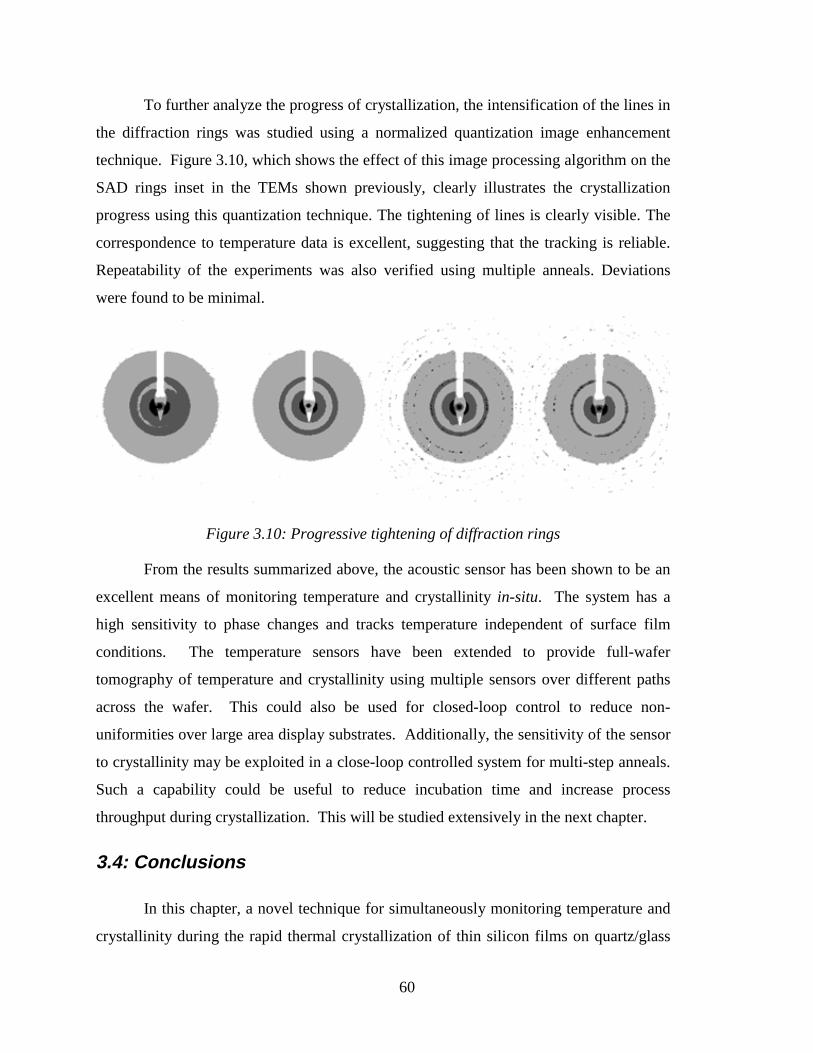
60
To further analyze the progress of crystallization, the intensification of the lines in
the diffraction rings was studied using a normalized quantization image enhancement
technique. Figure 3.10, which shows the effect of this image processing algorithm on the
SAD rings inset in the TEMs shown previously, clearly illustrates the crystallization
progress using this quantization technique. The tightening of lines is clearly visible. The
correspondence to temperature data is excellent, suggesting that the tracking is reliable.
Repeatability of the experiments was also verified using multiple anneals. Deviations
were found to be minimal.
Figure 3.10: Progressive tightening of diffraction rings
From the results summarized above, the acoustic sensor has been shown to be an
excellent means of monitoring temperature and crystallinity in-situ. The system has a
high sensitivity to phase changes and tracks temperature independent of surface film
conditions. The temperature sensors have been extended to provide full-wafer
tomography of temperature and crystallinity using multiple sensors over different paths
across the wafer. This could also be used for closed-loop control to reduce non-
uniformities over large area display substrates. Additionally, the sensitivity of the sensor
to crystallinity may be exploited in a close-loop controlled system for multi-step anneals.
Such a capability could be useful to reduce incubation time and increase process
throughput during crystallization. This will be studied extensively in the next chapter.
3.4: Conclusions
In this chapter, a novel technique for simultaneously monitoring temperature and
crystallinity during the rapid thermal crystallization of thin silicon films on quartz/glass
61
substrates has been presented. Previously developed acoustic sensors are used to
measure the variation of sound velocity with temperature, enabling the extraction of the
variation in elastic coefficients with temperature. From measured constants, it is possible
to extract the temperature of the substrates used. This technique for measuring
temperature is independent of surface emissivity and hence enables the tracking of film
crystallinity based on variations in optical absorbance, a new application of the sensor.
The technique has been demonstrated to be highly repeatable and sensitive. Phase
changes can be tracked from the onset of nucleation to full crystallization. This should
result in optimized techniques for the production of high performance, high throughput
glass compatible TFTs for AMLCD applications.

62

63
Chapter 4
Improvement of process throughput in solid-
phase crystallized TFTs using two-step annealing
___________________________________________
In chapter 3, a novel sensor for the detection of crystallinity and temperature
during rapid thermal crystallization of amorphous silicon on transparent substrates was
introduced. This sensor was shown to be sensitive to nucleation-type events, making it a
promising feedback control sensor for multi-step annealing. Since the onset of
crystallization can be detected, the potential exists for the use of independent anneal steps
to optimize initial nucleation and subsequent grain growth. In this chapter, thin film
transistors fabricated using such a control system are demonstrated as a proof of concept
[1]. A process is developed using multi-step annealing to substantially reduce process
time while improving device performance. The process exploits the independent control
of nucleation and grain growth achieved using the acoustic sensor.
In this chapter, a conceptual basis for multi-step annealing is introduced, along
with the experimental methodology for the fabrication of multi-step-annealed thin film
transistors. Electrical performance of the resulting devices is reviewed, placing emphasis
on the improvement in performance accompanying the substantial improvement in
process throughput. These results provide a demonstration of the concept of multi-step
annealing using in-situ control.
4.1: Conceptual basis for multi-step annealing
As was shown in chapter 2, both nucleation and grain growth are energy-activated
processes with characteristic activation energies. For the SPC Si system, the nucleation
activation energy is larger than the grain-growth activation energy. Therefore, SPC is
typically done at a low temperature to maximize grain size [2]. Unfortunately, this

64
results in a reduction in throughput through an increase in incubation time and a decrease
in the grain growth rate.
Rapid thermal crystallization, while offering high throughput, results in smaller
grain sizes due to the elevated temperatures used. Therefore, a method for reducing the
incubation time without sacrificing grain-growth thermodynamic conditions is highly
desirable. Multi-step annealing is well suited to this requirement [3]. A short high-
temperature step is used to nucleate the film, followed by a low-temperature step to
maximize grain size. Obviously, the ability to detect nucleation as the signal to initiate
the temperature quench is critical. The suitability of the acoustic sensor for use in this
role has been amply demonstrated in the previous chapter.
4.2: Experimental methodology
1000Å α-Si was deposited on fused silica wafers by LPCVD at 550°C/500mtorr
from SiH4. The wafers were annealed in the Stanford Rapid Thermal Multiprocessor [4].
The acoustic sensor was used for temperature / crystallinity tracking [5]. The samples
were heated to a substrate temperature of 700°C using tungsten halogen lamps. Note that
this temperature represents the average temperature measured along the acoustic path.
Additionally, the film temperature is expected to be somewhat different due to the
presence of vertical temperature gradients caused by the poor conductivity of fused silica.
Upon nucleation, the lamps were turned off and the wafers were placed into a furnace at
500°C for complete crystallization. Control samples were also processed. These were
either completely crystallized in the RTA or in the furnace. During the furnace anneals,
the extent of crystallization was checked every 24 hours. All crystallization was
performed in an argon ambient. Figure 4.1 illustrates the thermal processes. From this
figure, the decrease in temperature resulting from the onset of crystallization during RTA
is clearly visible. This decrease is used as the control signal for initiating the temperature
quench. The accuracy and the repeatability of this technique were established in the
previous chapter.

65
0
100
200
300
400
500
600
700
800
0 5 10 15 20Time (minutes)
Tem
per
atu
re (
C)
170hr
Single-step
RTA
Two-step
Onset of Crystallization.Temperature dip is due decrease in absorption.
Figure 4.1: Thermal cycles used during various crystallization anneals
Upon crystallization, the films were patterned and TFTs were fabricated using a
≤600°C planar top-gate self-aligned process, detailed in appendix 2. LPCVD SiO2 was
used as a gate dielectric, along with a SiGe gate electrode. This material was chosen for
its ease of dopant activation and high deposition rate. Ion implantation and furnace-based
dopant activation were used for source / drain / gate doping. Finally, the devices were
passivated in a hydrogen plasma. Electrical measurements were made. Plan-view TEMs
and selective area diffraction (SAD) measurements were also made at various stages
throughout the crystallization process.
4.3: Results and discussion
Figure 4.2 shows a plan-view TEM of the film at the point of the temperature
quench initiated by the acoustic sensor. Clearly, the film is at the onset of crystallization.
A few small crystallites (black in Figure 4.2) are present in a sea of amorphous material.
These act as growth-initiation centers during the low-temperature anneal.

66
Figure 4.2: Plan-view TEM showing film at start of quench in two-step process
Quenching to a low temperature retards further nucleation, and hence, post-SPC
grain size is larger than that for a single-step SPC film, which undergoes uniform
homogeneous nucleation. Average grain size measurements from plan-view TEM
indicate an increase in grain size of approximately 15%. This is accompanied by a seven-
fold reduction in crystallization time. For comparison, films crystallized using RTA
alone were also analyzed. The grain size is less than that for both one-step and two-step
furnace annealed films. The grain size was estimated by measuring the average area of
100 grains and determining the diameter of a circular grain of equal area.
Electrical characteristics for typical PMOS (Figure 4.3) and NMOS (Figure 4.4)
TFTs are shown below. Devices fabricated using two-step crystallization are superior to
one-step furnace crystallized TFTs. The improvement resulting from the two-step
process is visible in both the sub-threshold and on-state characteristics, suggesting a
general improvement in film quality and supporting the results seem in TEM. This
improvement in electrical performance is seen in several (>30) devices measured across
the wafer, indicative of good uniformity. Both the one-step and two-step annealed
devices exhibit better performance than TFTs fabricated using RTA crystallization, as is
expected from thermodynamic considerations. This is also in agreement with grain-size
measurements made using TEM.

67
-30-25-20-15-10-50510 -11
10 -10
10 -9
10 -8
10 -7
10 -6
10 -5
10 -4
Two-step SPCSingle-step SPCRTA
VG (Volts)
I D (A
)
PMOS
Figure 4.3: Electrical transfer characteristics for PMOS TFTs
-5 0 5 10 15 20 25 3010 -12
10 -11
10 -10
10 -9
10 -8
10 -7
10 -6
10 -5
10 -4
10 -3
Two-step SPCSingle-step SPCRTA
VG (Volts)
I D (A
)
NMOS
Figure 4.4: Electrical transfer characteristics of NMOS TFTs
Table 4-1 provides a summary of the parameters for the various devices. In all
cases, performance is best for devices fabricated using the two-step crystallization
process. Increases in field-effect mobility and sub-threshold slope accompany the
substantial improvement in process throughput. Threshold voltage is improved in PMOS
devices and is essentially unchanged in NMOS devices. This is probably a result of an

68
asymmetric distribution of grain-boundary states within the band-gap. Leakage current is
not changed substantially.
Table 4-1: Summary of device characteristics
Process Crystallization
Time
Grain
Size
Device Performance (W/L=20µm/20µm)
PMOS NMOS
µFE
(cm2/V⋅s)
sts
(V/dec)
VT
(V)
Imin
(pA/µm)
µFE
(cm2/V⋅s)
sts
(V/dec)
VT
(V)
Imin
(pA/µm)
RTA 15min 3500Å 18 1.8 -12.4 1.1 27 0.92 5 0.47
1-step
SPC
<168hr 4200Å 21 2.3 -9.9 6.1 34 0.69 5.6 0.24
2-step
SPC
<24hr 5000Å 28 1.4 -8.9 1.5 41 0.56 5.7 0.27
µFE is defined at |VDS|=0.1V, |VGS|<30V
VT is defined at |VDS|=10V, |ID|=100nA
Grain size is estimated from TEM by averaging the areas of 100 grains and calculating the diameter of a circle of equal area.
From the results shown above, the advantages of multi-step annealing are
obvious. A substantial improvement in process throughput along with an improvement in
device performance is achievable using this technology. The enhancement in
performance is a demonstration of concept of the multi-step annealing technology. The
incubation time is drastically reduced due to the initial high temperature step.
Subsequent nucleation is retarded by the temperature quench. This forms the conceptual
basis for controlled multi-step annealing.
An ultimate limit on this technology is imposed by the fact that the entire film is
heated during the initial nucleation step. Therefore, nucleation occurs randomly
throughout the film, and grain size enhancement is achieved because of probabilistic
considerations during the temperature quench. This places an ultimate limit on the
maximum possible grain-size enhancement. The next logical step, therefore, is to
develop a technology that allows selective nucleation of the film. This forms the basis of
the next chapter.

69
4.4: Conclusions
In this chapter, a controlled multi-step crystallization process has been used to
fabricate high-performance TFTs. A substantial improvement in process throughput and
device performance has been achieved using this technology. This provides a
demonstration of the concept of multi-step annealing. The two-step process allows
independent optimization of anneal steps for both nucleation and grain-growth processes.
Further optimization should enable greater improvements. Fast, high-temperature
nucleation should reduce substrate heating during RTA by increasing the temperature
gradient across the glass. This should allow the use of cheaper low-temperature glasses
to obtain a high-throughput, uniform polysilicon TFT process.

70
71
Chapter 5
Laterally crystallized polysilicon TFTs for AMLCD
applications using patterned light absorption
masks
___________________________________________
The two-step crystallization process used in chapter 4 results in a random
distribution of nuclei throughout the channel film as a result of the initial RTA step. In
this respect, the process is no different from a conventional low-temperature SPC
process. The nuclei formed during the high-temperature step subsequently enlarge to
enhance grain size. An ultimate limit on grain size enhancement is imposed by the fact
that the entire film has been exposed to the high-temperature step and will therefore
nucleate after the passage of some time during the low-temperature step. Hence, the
process is statistically limited in the maximum possible achievable grain-size
enhancement. A technique is therefore desirable to nucleate the channel films without
exposing the non-nucleated film to the same thermal cycle. This is the subject of this
chapter.
As in the last chapter, the acoustic sensor is used to detect crystallization in-situ.
However, in this chapter, a novel technique is used to increase heating selectively in
specific regions of the wafer. These regions nucleate first and form the starting points for
large laterally-crystallized grains grown during subsequent low-temperature annealing.
The technique used to achieve this is called patterned absorption masking [1]. Using this
technique, devices having extremely high-performance have been fabricated. In this
chapter, the conceptual basis for patterned absorption masking is introduced followed by
the process flow for the fabrication of high-performance TFTs using patterned absorption
masking. Experimental results obtained from such TFTs are reviewed, demonstrating the
performance enhancement achieved using this technique. Extensions to the technology

72
are discussed along with its applications to the fabrication of large area active matrix
displays.
5.1: Conceptual basis for patterned absorption masking
At tungsten-halogen wavelengths, silicon is a poor absorber of light. A large
fraction of the light is transmitted through the thin silicon film, resulting in inefficient
heating of the substrate. The absorption coefficient of silicon is shown below (Figure
5.1), along with the radiant spectra for a typical tungsten-halogen and Xenon arc lamp
[2].
Figure 5.1: Silicon absorption and radiant spectra for typical RTA lamps

73
Besides the intrinsically inefficient heating due to poor heat transfer, substantial
heat is also lost to the surroundings through convective and radiative losses. The ability
to locally increase the heating of the silicon through increased light absorption enables
the selective nucleation of the channel films. This local increase in light absorption is
facilitated using patterned thick layers of an absorbing material over the region to be
nucleated; heat is conducted to this region from the absorbing layer, resulting in a
temperature gradient in the channel film away from the heat absorbing seed point. This is
shown schematically below (Figure 5.2). The temperature gradient, induced by the
patterned absorption masks, results in nucleation under the mask without exposing the
surrounding region to the same thermal cycle. This system can therefore be used for
controlled seeding and grain-size enhancement using lateral crystallization.
Channel Film
Etch Stop SiO2
Mask Layer
Loss to surroundings
Conductionto Channel
Film
Lateral T gradientConduction to
substrate,Vertical Tgradient
Direct HeatAbsorptionby channel
Heat absorption by mask
Figure 5.2: Heat flow during RTA using patterned absorption masks

74
5.2: Experimental details
100nm amorphous silicon was deposited on fused silica substrates by LPCVD at
525°C/1000mtorr from SiH4. An etch stop layer of 20nm LPCVD SiO2 (LTO) was
deposited on top of the amorphous silicon, followed by 300nm of an amorphous silicon
masking layer. Amorphous silicon was used for simplicity; materials with higher
absorption coefficients, such as SiGe, could be used to enhance the masking effect.
The masking layer was patterned to form islands over the regions to be used as
the TFT drains. The wafers were then subjected to an RTA nucleation step in the
Stanford Rapid Thermal Multiprocessor [3]. The time required for the RTA step was
determined using the acoustic sensor. Wafers with no masking layer were found to
nucleate in 380 seconds. Wafers with a blanket masking layer were found to nucleate in
75 seconds. Interestingly, the substrate temperature was found to be essentially the same
in both cases, 750°C, indicative of a substantial vertical temperature gradient. Device
wafers with patterned masking layers were nucleated in 300 seconds. This verifies the
heat loss to the surrounding unmasked films through a conductive process and establishes
the presence of a temperature gradient. Using a test pattern of broad (1mm) lines and
spaces, the selective nucleation was visually identifiable, with the unmasked regions
being more opaque than the masked regions upon mask removal.
After nucleation, the wafers were crystallized in a furnace at 500-550°C in argon.
The masking layers were then etched off. The etch stop SiO2 was removed in HF, and
standard top-gate self-aligned planar TFTs were fabricated using a glass-compatible
(<600°C) process. The complete process flow is shown below (Figure 5.3). For
comparison, control devices were fabricated using LT-SPC and RTA.
Electrical measurements were made on the devices to determine performance
characteristics. Plan-view TEMs were also made on test structures to verify the seeding
process (inset, Figure 5.3). This figure shows the partially grown seeded region in an
amorphous matrix.

75
Transparent Substrate
Channel α-Si
Transparent Substrate
Mask α-Si
Etch Stop SiO2
Transparent Substrate
Channel α-Si
α-Si
Temperature Gradient
Homogenous Nucleation(elongated grains due to gradient)
Lateral Crystallization
1) Deposit channel
2) Deposit etch stop & mask
3) Pattern mask
4) Nucleate using RTA
5) Crystallize using LT-SPC
6) Remove mask & etch stop
7) Fabricate TFT
Figure 5.3: Process flow for laterally crystallized TFTs (inset: TEM of seeded grain
growth)
5.3: Results and discussion
Device transfer characteristics for a 2µm / 2µm device are shown below (Figure
5.3). From this figure, it is apparent that the performance of absorption-masked devices
is substantially better than that of conventional devices, both in terms of on-current and
sub-threshold performance.

76
1.E-12
1.E-11
1.E-10
1.E-09
1.E-08
1.E-07
1.E-06
1.E-05
1.E-04
-10 -5 0 5 10 15 20VG (V)
I D (
A)
Control
Seeded
VD=5V
VD=0.1V
(a) W/L=2µm/2µm
Figure 5.4: Electrical characteristics of 2µm/2µm TFTs
The electrical characteristics are summarized below (Table 5-1). Both NMOS
and PMOS field-effect mobility values show an improvement of greater than 50% for the
laterally crystallized devices. Sub-threshold slope also shows an improvement of
approximately 25%. Leakage current stays essentially unchanged within the noise limits
of the measurement system.
Table 5-1: Device characteristics for 2µm/2µm TFTs
NMOS PMOSParameter
Conventional Laterally
Crystallized
Conventional Laterally
Crystallized
µFE (cm2/V-s) 41 65 15 24
Imin (pA/µm) 6 8 -8 -6
sts (V/dec.) 0.64 0.49 -1.0 -0.77

77
Maximum performance enhancement was achieved for small devices. Device
transfer characteristics for a 20µm / 20µm device are shown below (Figure 5.5). From
this figure, it is apparent that, though there is some improvement in performance of these
larger devices, the improvement is less than that seen for smaller devices. In all cases,
however, there is clear improvement in both on-state and sub-threshold performance.
1.E-12
1.E-11
1.E-10
1.E-09
1.E-08
1.E-07
1.E-06
1.E-05
1.E-04
1.E-03
-10 0 10 20 30VG (V)
I D (
A)
Control
Seeded
VD=10V
VD=0.1V
(b) W/L=20µm/20µm
Figure 5.5: Electrical characteristics of 20µm/20µm NMOS TFTs.
A measure of the extent of lateral crystallization can be obtained by analyzing the
variation in performance improvement with device geometry; this is done below. Figure
5.6 shows the variation in mobility vs. channel length. Figure 5.7 shows the variation in
mobility improvement vs. device geometry, relative to the control devices. This mobility
improvement is calculated as a fraction of the field-effect mobility of the conventional
control device. From these figures, it is clear that smaller devices show greater
improvement than larger devices, and that the trend is monotonic in nature. Also, it is
evident that for devices larger than several microns, the amount of improvement is
constant, indicative of the enhanced grain structure shown in the process flow. This is
discussed below.

78
30
35
40
45
50
55
60
65
70
0 5 10 15 20
Drawn Channel Length, L (µm)
Fie
ld-e
ffec
t M
ob
ility
, µF
E (
cm2 /V
-s)
Control
Seeded
Figure 5.6: Variation in NMOS field effect mobility with channel length
2 4 6 8 10 15 20
1
2
6
10
20
0
10
20
30
40
50
60
70
imp
rove
men
t (%
)
L (µm)
W (µm)
Figure 5.7: Variation in NMOS field-effect mobility improvement with device size
In all cases, seeded devices have better performance than unseeded devices. The
increase in performance improvement with decreasing device size is explained by the fact
that the laterally crystallized region of the channel becomes an increasing fraction of the

79
channel length and width as geometry is reduced. Therefore, this technique works best
for small devices. For larger devices, there is still some improvement achieved using the
absorption masks. This is explained by the fact that the laterally crystallized region
extends into the drain field of the TFT for devices of all sizes. This reduces scattering in
the same, improving performance in all cases. Additionally, TEM analysis indicates that
all grains are elongated slightly, including those wholly formed away from the absorption
masks. It is suspected that this phenomenon is a result of the temperature gradient
experienced by the film during RTA. This elongation of grains may also partially explain
the improvement in performance seen in larger devices.
The main advantage of this seeding technique in comparison to other techniques
is its simplicity. Since no seeding material is in physical contact with the channel film,
this is a non-contact seeding technique, suffering from no potential contamination issues.
Additionally, since the seeding is performed using commonly available equipment and
materials and involves only one extra lithographic step, the cost of implementation of this
technique is expected to be low.
Patterned absorption masking is also promising as a technique to tune the device
characteristics across a single substrate. Lateral crystallization as demonstrated in this
work can be used to fabricate high performance TFTs. Controlled seeding of large grains
enhances performance without causing substantial statistical variation in channel
structure. Unmasked structures can be used to fabricate standard TFTs. A fully masked
structure can be used to cause extensive nucleation throughout the TFT, resulting in a
small-grain TFT structure with low statistical variation in mobility, useful when small
TFTs are desired. To facilitate the use of lateral crystallization on larger TFTs, a matrix
of masking points can be used, resulting in a larger average grain size. These structures
are shown schematically below (Figure 5.8).

80
S D
Gate
S D
Gate
S D
Gate
MaskS D
Gate
B) Laterally Cryst.A) Standard
C) Small grain D) Large grain
Mask
Mask
Figure 5.8: Plan-view of mask structures to achieve (a) standard (b) laterally crystallized
(c) small grain (d) large-grain TFTs
To enable a proper understanding of the absorption masking process, it is useful
to perform an analysis of the heat flow within the system. This is conveniently done by
using an electrical equivalent circuit. A pattern of lines and spaces is simplified into a
simple line and space pattern by exploiting symmetry considerations, which dictate that
no heat will flow across the symmetry planes. This simplified system is then replaced by
an equivalent electrical circuit. Figure 5.9 shows this process schematically. In this
figure, various analogues are made, as detailed below.
Table 5-2: Thermal and electrical analogues
Thermal Parameter Electrical EquivalentTemperature T Voltage VHeat flow H Current IThermal resistance
Ak
x
⋅∆ Electrical Resistance R
Conductive loss
dx
dTAkH ⋅⋅=
Resistive loss
R
VI =
Heat stored tHQ ∆⋅= Charge stored tIQ ∆⋅=Temperature change QcTT P ∆⋅+= 0
Voltage change
C
QVV += 0

81
Substrate
Channel Film
Mask
ThermalCapacity
4C
Conduction4R
ConductionR
ThermalCapacity
CConductive loss to
substrateIsub
Heat fromlamp4Ilamp
ConvectivelossIconv
Radiative lossIrad
Reduction by symmetry
Heat fromlampIlamp
Conductive loss tosubstrate
Isub
ConvectivelossIconv
Radiative lossIrad
Figure 5.9: Extraction of electrical equivalent of heat flow
The important points to note are:
1. The generation of heat in the film and mask is essentially proportional to the film and
mask thickesses respectively, for systems with films and masks made of identical
materials.
2. Losses from the film and mask regions are essentially the same if lateral radiative and
convective losses are ignored.
82
To prove that a temperature gradient is indeed induced in the film, consider the
case in which there are no losses. In this situation, after an initial transient, there will be
no temperature gradient, as the capacitors will charge up. For thin Si films, this transient
is quite small, typically on the order of milliseconds or seconds, and definitely not on the
order of hundreds of seconds as used in device fabrication. To account for this, the effect
of losses must be included.
Consider the other extreme, in which the losses exceed the heat input. This
situation would result in cooling rather than heating, and is therefore incorrect. Consider
then the case in which there is substantial heat loss, but it is less than the heat input to the
system. For example, consider the case where the heat loss is greater than the heat
generated within the film, but is less than the heat generated within the mask. In this
case, the system essentially is limited by the resistive divider formed by the conductance
resistances and the loss current sources. Hence, a temperature gradient can be sustained
for infinite time in this case. In real systems, losses are not this high, and in fact, losses
will typically be less than the heat generation within the film. In this case, the gradient
will slowly decrease, but may be substantial for tens or even hundreds of seconds,
depending on the ratio of heat loss to heat generation. Since the heat loss is essentially
proportional to the surface area, and the heat generation is essentially proportional to the
volume, the net gradient is a function of the surface to volume ratios of the mask and
film. Since the mask is much thicker than the film and therefore has a smaller area to
volume ratio, a temperature gradient can be sustained from the mask to the film for long
periods of time, depending on the precise loss and heating parameters. These may be
optimized to enhance the gradient. The heating profiles may also be optimized to exploit
the transient nature of the gradient. In general, performing such an analysis provides a
clear guideline for optimization of the absorption masking technology in general.
The experiments detailed in this chapter can be quantitatively analyzed using a
technique similar to that discussed above. The resistive / capacitive network shown
above (Figure 5.9) can be simplified to a lumped model for convenience, to enable an
intuitive appreciation of the process. The parameters for the system were conveniently
determined using a test structure of lines and spaces implemented on the wafers in
question. Table 5-2 enables the determination of the RC time constant representing the

83
time before the unmasked regions in the lines and spaces array heat up, based on known
values of silicon conductivity (approximately 150W/m⋅K) and heat capacity
(approximately 700J/kg⋅K). If we ignore the effect of heat losses, this time is found to be
only 0.4 seconds, in agreement with results determined by other authors for transient
rapid thermal annealing using highly efficient arc lamps [2]. However, if we account for
losses due to the inefficient heating of thin Si films by tungsten-halogen lamps (Figure
5.1), this time constant increases substantially. For example, by considering only
radiative losses to the chamber, the calculated RC time constant increases substantially,
to 140 seconds, as shown below.
ConstCRLossless =⋅
Equation 5-1
( )4TAH Radiation ∆⋅⋅⋅=∈ σ
Equation 5-2
where:
∈ is the emissivity of Si (approximately 0.6)
σ is Boltzmann’s constant
A is the surface area
∆T is the temperature difference relative to the ambient
An equivalent resistance may be conveniently substituted for the current source
used above (Figure 5.9), by taking the derivative of the temperature (voltage) relative to
the loss (current). This may then be inserted into the equivalent circuit. By
approximating the heat as a Thevenin’s equivalent circuit, the relationship between the
time constants is established.
+⋅=
Loss
LossLosslessLossy R
RRRCRC
Equation 5-3
84
Clearly, as the loss increases relative to the intrinsic heat flow, the lossy time
constant will increase relative to the ideal time constant (Equation 5-1), as is evident
from the calculated results. Experimentally, the lines and spaces array provides an
estimated time to wide-spread nucleation of approximately 400 seconds, which is
reasonably close to the predicted value, given the fact that the above analysis ignores
convective losses entirely.
This analysis can be extended further to predict the probability of nucleation by
using the activation energy discussed in chapter 2. By integrating the nucleation rates
over the entire thermal cycle (ignoring the ramp-time), after the passage of RC time the
probability of nucleation away from the mask is approximately 2% of that under the
mask. This, in fact, is the reason absorption masking-based seeding is possible, and thus,
the theoretical basis for this technique is established.
5.4: Conclusions
In this chapter, a novel lateral crystallization technique has been described which
utilizes a two-step crystallization process. Patterned light absorption masks are used
during an initial rapid thermal annealing step to initiate nucleation in the drain region of
TFT channel films through increased heating of the amorphous silicon under the masks.
Upon detection of nucleation, the films are annealed at low temperature, resulting in
lateral crystallization into the channel region of the transistors. This results in a
substantial improvement in device performance.
The effect of device geometry on the amount of improvement has been analyzed,
and novel mask structures have been proposed to enable fabrication of widely differing
TFTs on a single substrate. The non-contact nature of this seeding technique, coupled
with its simplicity, makes it a promising technique for the fabrication of high
performance TFTs for AMLCD applications. The technique also demonstrates the use of
sophisticated anneal techniques to independently control the nucleation of a crystallizing
silicon film relative to the grain-growth.

85
Chapter 6
Optimization of amorphous precursor
characteristics of silicon-germanium alloys
___________________________________________
At this point, it is appropriate to digress somewhat and discuss the effect of the
quality of the amorphous film on the electrical characteristics of the finished TFT. In
previous chapters, various techniques to enhance grain size have been discussed.
Intuitively, and from the theory described in chapter 2, the quality of the amorphous film
is expected to affect the quality of the crystallized film. As identified in that chapter, the
quality of an amorphous silicon film is a strong function of the deposition conditions.
The effect of deposition conditions on the quality of amorphous silicon has been studied
extensively [1]. Therefore, in this chapter, a similar study will be performed on the
deposition of silicon-germanium for three reasons. Firstly, silicon-germanium (Si1-xGex,
hereafter referred to as SiGe) is a promising candidate for use as a TFT channel film [2].
Secondly, in chapter 7, silicon-germanium will be used to demonstrate a new type of
lateral crystallization, germanium-seeded lateral crystallization. Thirdly, as a deposition
system, SiGe is affected by several interesting phenomena, making it a useful test vehicle
for the deposition / crystallization theories developed in chapter 2.
SiGe TFTs fabricated using low-temperature solid-phase crystallization (LT-SPC)
have already been demonstrated [3]. For LT-SPC applications, SiGe is particularly
advantageous, as it requires substantially shorter annealing cycles than required for the
crystallization of Si. SiGe TFTs fabricated using scanned rapid thermal annealing (RTA)
have also been demonstrated [4]. SiGe is advantageous for scanned RTA processes, as it
requires lower crystallization temperatures, reducing glass warpage. To date, using
conventional SPC processing with no pre-amorphization implant, SiGe TFT performance
has generally been worse than poly-Si TFT performance [3]. SiGe TFT performance has
been improved substantially through the use of a thin Si interlayer to improve the gate

86
oxide interface [5]. However, little has been done to improve the intrinsic quality of the
SiGe channel film itself; the binary nature of the SiGe system complicates optimization
and modeling substantially.
In this chapter, the results of response surface characterization studies performed
on the low-pressure chemical vapor deposition (LPCVD) of SiGe for the fabrication of
TFTs are described. First, background information on the deposition of silicon-
germanium and on the use of statistical design of experiments is provided. Experiments
performed using such a design are described, and the results of these experiments are
used to develop a qualitative atomistic model of the deposition, explaining the noted
variation in electrical results with changes in the deposition conditions. Optimization
strategies for the fabrication of high-performance SiGe TFTs are developed and the
limitations of such strategies are discussed and quantitatively analyzed.
6.1: Background information
6.1.1: Silicon-germanium deposition
Silicon-germanium is easily deposited by LPCVD from silane (SiH4) and
germane (GeH4). To obtain amorphous films, deposition temperatures are usually lower
than those required for the LPCVD of amorphous silicon [2]. This has been explained as
a catalysis effect of germane [6]. Germanium species on the growing surface result in
increased hydrogen desorption at any given temperature. Since this desorption is the rate
limiting process in the deposition of silicon, this results in the observed increase in
deposition rate.
The transition temperature for deposition in the amorphous phase to deposition in
the polycrystalline phase is also lowered for SiGe. Therefore, SiGe depositions for the
formation of TFT channel films are typically done at lower temperatures than those used
for Si films. This ensures the formation of high-quality amorphous silicon-germanium
films. Upon crystallization, these films form large grain poly-SiGe, suitable for the
fabrication of polycrystalline TFTs.
Several factors affect the quality of the deposited amorphous SiGe. The
deposition rate is a function of the temperature, pressure, and germanium fraction in the
87
film. The germanium fraction in the film is itself a function of temperature and germane
partial pressure relative to silane partial pressure. Therefore, the deposition of SiGe is a
complex function of temperature, pressure and germane and silane partial pressures, and
has been studied extensively [7]. The quality of the amorphous film is a function of the
deposition parameters, as per the theory developed in chapter 2. Additionally, for the
deposition of SiGe on SiO2, it is necessary to deposit a thin seed layer of silicon on the
oxide surface. This ensures the formation of a smooth channel film. Germanium
deposition on oxide is not energetically favorable; therefore, failure to use a seed layer
results in the deposition of rough films due to the initial clustering of germanium species
on the growing surface. The use of a silicon seed layer solves this problem, but increases
the complexity of the analysis.
Given the numerous factors affecting the deposition and quality of amorphous
silicon-germanium films, a systematic analysis of the same using standard factorial
experimental design schemes is tedious and impractical; the problem is suitable for
preliminary analysis using a multifactorial design of experiments
6.1.2: Design of experiments
To enable the analysis of the deposition of SiGe, several process parameters of
importance were identified using a Plackett-Burman screening experiment [8]. In this
design, two discrete experimental conditions are chosen for a variety of experimental
variables. The conditions are placed at the extrema of the expected experimental space,
and certain sets of conditions are eliminated based on the assumption that they will
exhibit themselves in combinations of other sets of conditions. This therefore provides a
convenient means of identification of parameters of potential importance from a reduced
set of experiments. The quantitative accuracy of this technique is low, but it provides the
ability to detect important trends, since it is highly unlikely that the variables will
completely reflect back on themselves at the two chosen conditions. Based on the results
of this experiment, detailed in [9], various parameters in need of further study were
identified. These are the deposition pressure, temperature, and seed layer thickness. For
reduced design complexity and size, germanium fraction was eliminated as a variable.
All TFTs were fabricated with a 17% Ge fraction. This fraction was chosen based on its

88
high hall mobility [10], compatibility with conventional cleaning solutions, and ease of
deposition. An experimental design space was selected for the three variables. The
temperature range was chosen based on the requirements of amorphous film deposition
(defined the upper limit) and reasonable deposition rates (defined the lower limit). The
pressure range was selected based on the technological restrictions imposed by the
deposition system. The seed layer thickness range was chosen based on the thickness
ensuring full surface coverage (defined the lower limit). The upper limit of seed layer
thickness was chosen to be small, based on the results of the screening experiment.
Upon definition of the experimental design space, a design was developed using
standard design techniques. Provided certain assumptions are made about the nature of
variations (e.g., second order, logarithmic, or exponential dependencies), several
experimental conditions can be eliminated from standard multifactorial designs by
carefully choosing the positions of the experimental conditions. For example, by
assuming first and second order trends and interactions, a design space can be completely
deconvolved from a design that has experimental conditions set at the vertices of a cube
(for a three variables design), with additional conditions at a specific ratio along the
individual axes. The precise number of points used determines the accuracy of the
model. The design chosen here enables detection of first and second order trends. More
sophisticated models could also be applied to the design results to enable detection of
various non-linear effects. The design space is shown schematically below (Figure 6.1).
Figure 6.1: Definition of experimental design space

89
6.2: Experimental details
All devices were fabricated on fused silica wafers. 100nm LPCVD (LTO) SiO2
was deposited on the substrates, for use as a barrier / smoothing layer. On this,
amorphous channel films were deposited based on the conditions described above (Figure
6.1). The equipment used for deposition was a hot-wall tubular LPCVD system. The Si
seed layer deposition was followed by the SiGe deposition without breaking vacuum.
Subsequently, the films were crystallized in a furnace at 550°C in an argon ambient.
After crystallization, the active regions were patterned. 100nm LPCVD (SiO2) was
deposited as the gate dielectric and annealed in Ar at 550°C for 6 hours. This was
followed by 250nm Si0.6Ge0.4, which was used as the gate electrode. This film was
chosen based on its high deposition rate at low temperatures (500°C) and its ease of
dopant activation (<2 hours at 550°C). Gates were defined, and doping was performed
using ion-implantation. Dopants were activated at 550°C. All dopants were activated
within 4 hours. After dopant activation, devices were passivated with LTO, contacts
were formed, and metallization was performed using Al. The maximum process
temperature was therefore 550°C, ensuring compatibility with low-cost glass substrates.
The wafers were plasma hydrogenated in a parallel plate system for 8 hours, and
electrical measurements were made. A cross-section of the device structure is shown
below (Figure 6.2). Plan-view TEM analysis was also performed on selected samples to
determine the average grain size.
Fused Silica Substrate
LTO Barrier / Smoothing Layer
SiGe Channel
SiGe GateElectrode
Source Drain
LTO Gate oxide
Si Seed LayerIon Implanted
Figure 6.2: Cross-section of SiGe TFT

90
To test the accuracy of the model results, further devices were also fabricated as
test devices. Deposition condition points were chosen away from the model vertices,
near the edges of the experimental space, and near the center point. Results were
compared to model predictions to determine model accuracy.
To accompany the device fabrication experiments, several experiments were also
performed to analyze the properties of the deposition process. Films of both amorphous
silicon and silicon-germanium were deposited on oxidized silicon substrates at various
temperatures and pressures, and the deposition rates under these conditions was
monitored. The deposition equipment was also monitored for the onset of gas-phase
nucleation (discussed later). This was done by examining the substrates and the
deposition equipment itself for the presence of particulates of deposited Si and SiGe.
6.3: Results and discussion
Various electrical parameters were extracted from the measured current-voltage
curves, including field-effect mobility, leakage current, sub-threshold slope, and
threshold voltage. Response surfaces were generated for the various parameters using
first and second order effects and interactions. Over the ranges of temperature, pressure
and seed thickness used, it was expected that such models would provide good predictive
ability. In general, it was found that all parameters demonstrated similar trends versus
temperature and pressure, i.e., conditions that resulted in high mobility also resulted in
steep sub-threshold slope. It was also found that seed thickness generally has little effect
on device performance over the ranges studied. Temperature and pressure, on the other
hand, greatly affect device performance. The effect of temperature and pressure on
device performance is shown below (Figure 6.3 and Figure 6.4). These figures show the
variation in NMOS and PMOS field-effect mobility with changes in deposition
temperature and pressure. The plots are the theoretical response surfaces generated from
the experimental data gathered at the specified deposition conditions. Figure 6.3 also
shows the location of some of the data points used in analsis.

91
0
10
20
30
40
N_µ FE_PT
µFE (cm2/V-s)
250
1000
Pressure (mtorr)
460
510
Temperature (°C)
Figure 6.3 Response surface of NMOS mobility
To test the accuracy of the model, predicted values of field-effect mobility can be
compared to experimentally determined values of the same.
Table 6-1: Comparison of theoretical and experimental mobility values.
Deposition Conditions NMOS Field-effect mobility
(cm2/V-s)
Temperature(°C)
Pressure(mtorr)
Seed Thickness(Å)
Theory Experiment
485 625 50 18 19
485 1000 50 27 26
485 250 50 16 13
510 625 50 4.8 5.8
460 625 50 22 18

92
0
10
20
30
40
50
P_µ FE_PT
µFE (cm2/V-s)
250
1000
Pressure (mtorr)
460
510
Temperature (°C)
Figure 6.4: Response surface of PMOS mobility
From the response surfaces, it is apparent that performance improves with
increasing pressure and decreasing temperature. At the lowest ranges of temperature and
pressure, there is a saturation in improvement; indeed, some degradation is evident under
some conditions. At intermediate temperatures and high pressures, performance is
maximum, and importantly, performance improvement is not saturated, suggesting that
further improvement can be achieved by increasing the ranges of pressure studied.
Confirmation experiments verify these trends, suggesting that the predictive capabilities
of the response surfaces are good. Within the ranges of temperature, pressure, and seed
thickness used, SiGe TFTs having higher performance than previously achieved using
any similar technology have been demonstrated. The transfer characteristics for sample
NMOS and PMOS TFTs are shown below (Figure 6.5 and Figure 6.6). Electrical
parameters are summarized as well (Table 6-2).

93
1.E-12
1.E-11
1.E-10
1.E-09
1.E-08
1.E-07
1.E-06
1.E-05
1.E-04
1.E-03
-10 -5 0 5 10 15 20 25 30
VGS (V)
I D (
A)
VDS=10V
VDS=0.1V
(a) NMOS (W/L=20µm/20µm)
Figure 6.5: Transfer characteristic of sample NMOS TFT
1.E-12
1.E-11
1.E-10
1.E-09
1.E-08
1.E-07
1.E-06
1.E-05
1.E-04
1.E-03
-30-25-20-15-10-50510
VGS (V)
-ID (
A)
VDS=-10V
VDS=-0.1V
(b) PMOS (W/L=20µm/20µm)
Figure 6.6: Transfer characteristics of sample PMOS TFTs

94
Table 6-2: Summary of device characteristics
Parameter Range of results
NMOS PMOS
Worst Best Worst Best
Field-effect mobility, µFE (cm2/V-s) 5 38 6 44
Threshold Voltage, VT (V) 12 5.5 -1.5 -8.5
Sub-threshold slope, sts (V/decade) 2.4 1.5 2.3 1.1
leakage current, Ioff (pA/µm) 12 7 3 0.8
Field-effect mobility is defined as the maximum mobility achieved for VDS=|0.1V|, VGS<40V
Threshold Voltage is defined at ID=100nA⋅(W/L), VDS=|10V|
Sub-threshold slope and leakage current are defined at VDS=10V
For any given deposition condition, the uniformity of device electrical
performance was found to be good. In general, since the test devices used for electrical
parameter extraction were large (W/L=20µm/20µm), variations in electrical behavior due
to statistical variations in grain distributions were averaged out. Standard deviation was
typically less than 10% for a sample size of approximately 20 devices. Based on
confirmation experiments, the accuracy of the response surfaces has been found to be
excellent over the ranges of temperature and pressure studied. Some deviation in actual
and predicted values is evident near the boundaries of the experimental space. Predictive
accuracy is better than 10% near the center of the experimental space, and is better than
20% near the edges. In all cases, the trend prediction has been found to be accurate, with
only a slight quantitative discrepancy. Indeed, the trend prediction has been found to be
satisfactory beyond the experimental space as well. In particular, the effects of pressure
are predicted with less than 20% deviation to ranges nearing 2 Torr. The model’s
predictive ability for the effects of temperature is less accurate, with deviations exceeding
25% at temperatures 25°C beyond the experimental ranges studied here.
The trends determined experimentally are easily explained using conventional Si-
based atomistic models of LPCVD [11], as developed in chapter 2. With decreasing
temperature, the surface diffusivity of physisorbed Si species is reduced. This reduces

95
the amount of surface organization that occurs before chemical bonding, thereby reducing
the number of locally organized entities formed within the amorphous film. During
crystallization, this corresponds to a reduction in nucleation sites present within the film,
resulting in TFTs having larger average grain size, and hence, better performance.
Increased deposition pressure results in an increased flux to the surface, and hence
reduces the physisorbed lifetime on the surface prior to chemical bonding. Therefore,
this also decreases the concentration of locally organized entities. The process is shown
schematically below (Figure 6.7). At the lowest temperatures and highest pressures, the
concentration of locally organized entities within the amorphous film is low enough that
homogeneous nucleation within the amorphous matrix starts to dominate, resulting in the
saturation and rebound observed in the electrical characteristics of the TFTs. This is
easily explained using the model of pre-existing nucleus formation described in chapter 2
in section 2.2.2. At low temperatures and high pressures, the concentration of nuclei
within the amorphous film is extremely low and nucleation occurs primarily through
homogeneous means. As the pressure is reduced, some nuclei are introduced into the
amorphous matrix. These grow during the incubation time to increase the average grain
size within the film, and hence, at low temperatures, going from an intermediate to a high
pressure actually degrades the device performance.
Substrate
AmorphousLayer
Formation
LocallyOrganizedNucleation
Site
ImpingingFlux
Physisorptionand Surface
Diffusion
Figure 6.7: Schematic view of atomistic deposition model

96
This model is supported by a qualitative analysis of grain size obtained via TEM.
In all cases, grains are typically elliptical in nature. Grain size was estimated by
averaging the area of 100 grains and determining the diameter of a circle of equal area.
Average grain size for the best channel films was found to be approximately 6500Å,
while the average grain size for the worst channel films was found to be somewhat lower,
approximately 4000Å. In general, while the largest grains in all films appear to be
roughly the same size, the density of smaller grains is higher for the poor quality films,
resulting in the decrease in average grain size. Additionally, all grains show evidence of
intra-grain defects, seen by other authors for SPC films [12]; the concentration of these
defects is visually higher in the poor quality films deposited at higher temperatures and
lower pressures. Both of these observations are expected results of the locally organized
entity incorporation discussed above and in chapter 2, since the presence of sub-critical
organized entities in the amorphous film increases nucleation and dendritic growth.
The atomistic model discussed above suggests a clear optimization strategy for
SiGe TFTs, i.e., an increase in the deposition pressure and a decrease in the deposition
temperature. Clearly, such a strategy has practical limitations. In particular, at higher
deposition pressures, gas-phase nucleation occurs, resulting in rough, defective, and poor
quality films. In this regime, however, results suggest that SiGe may offer some
advantages over Si. As mentioned above, Ge is a catalyst for the deposition of Si. It
causes increased hydrogen desorption, increasing the deposition rate. This effect is
therefore a surface effect. The effect of Ge on gas-phase reactions between Si atoms is
not expected to be the same, since the process would require a greater germane partial
pressure than present, resulting in reduced probability based on simple atomistic models.
For a given deposition rate at a low pressure of say, 100mtorr, SiGe can be
deposited at a lower temperature than Si. As the pressure is increased, the deposition
rates of both SiGe and Si increase. However, at high pressures, the onset of gas-phase
nucleation occurs in the Si deposition system. This point is offset to higher pressures in
SiGe deposition, based on the lower deposition temperature, and hence lower gas-phase
reactivity. This essentially amounts to an increase in the optimization space for SiGe
deposition over that available for Si deposition. Based on the response surfaces described
previously, this corresponds to an increased maximum device performance.

97
Figure 6.8 shows the relative deposition rates and onset of gas-phase nucleation of
Si and SiGe versus pressure for a similar deposition rate at low pressure.
0
5
10
15
20
25
30
35
40
45
50
0 200 400 600 800 1000 1200
Deposition Pressure (mtorr)
Dep
osi
tio
n R
ate
(A/m
in)
Si, 550C
20% SiGe, 500C
Gas-phase nucleation occurs in Si
No gas-phase nucleation in SiGe
Figure 6.8: Characterization of onset of gas-phase nucleation in Si and Si0.8Ge0.2
Figure 6.9 shows a schematic of the atomistic processes of catalysis. The
differences in the shape of the deposition rate vs. pressure curves shown above (Figure
6.8) are strongly indicative of the catalysis process. The SiGe deposition curve shows a
typical catalyzed reaction behavior [13].
Substrate
H
Impinging Flux
No Gas-phase
nucleationdue to lowertemperature,
reactivity
Surface reaction increased byGe-mediated hydrogen
desorption
GeSi
Substrate
SpeciesConcentration,
Reactivity istoo high!!
Formation ofcluster ingas-phase
Over-abundance of
nucleationsites, voids,
rough surface
Impinging Flux
(a) (b)
Figure 6.9: Schematic view of (a) gas-phase nucleation and (b) the effect of Ge catalysis
on the same

98
The deposition is well described by a Michaelis-Menten equation as described in
chapter 2, except surface sites are now provided by Ge-mediated H-desorption:
Pk
PEkR
M
tot
+⋅⋅
= 2
Equation 6-1
where:
k2 and kM are constants
Etot is the total amount of catalysis sites available
P is the deposition pressure
R is the deposition rate
Here, as in chapter 2, we make the simplifying assumption that the main rate-
limiting reaction occurs in two stages:
xk
k
x SiHSiH ⋅←→
+−
**1
1
Equation 6-2
↑⋅+⋅→⋅ HxSiSiH kx ** 2
Equation 6-3
where:
* is a bonding surface site
SiHx is a silicon hydride species physisorbed to the surface
k1, k-1, k2 are rate constants
We assume that the first reaction includes the formation of the bonding site, *,
within the rate constant k1. As shown in chapter 2, for typical Si and SiGe reactions, this
is hydrogen desorption limited. Assuming concentration-dependent reactions:
1
21
k
kkkM
+= −
Equation 6-4

99
For the case where hydrogen desorption is restricted, k1 is small, and kM becomes
large. As kM becomes larger, the reaction rate equation (Equation 6-1) results in more
linear behavior with pressure. Figure 6.8 shows that this is indeed the case for Si.
The total number of Ge-catalysis sites available is a function of the equilibrium
surface coverage by germanium, the H-desorption from these sites (assuming that H-
desorption from these sites is much faster than desorption from Si-sites) and the total
number of surface sites. Thus, at a constant germanium fraction, this number is
essentially constant, resulting in the characteristic curve shown previously (Figure 6.8).
The Si deposition curve, on the other hand, exhibits a much more linear variation with
pressure at the temperature used. Higher temperatures are required to deposit Si than
those required to deposit SiGe at the same deposition rate and pressure. This results in
increased gas-phase reactivity and hence an increased probability of gas-phase
nucleation. Again, the catalyst effect of Ge is not evident in the gas-phase for low
germane partial pressures, since the effect is a surface effect. For Ge to catalyze the gas-
phase reaction, a substantially higher germane partial pressure is required. At typical
deposition temperatures, the gas-fraction of Ge-species is substantially less than the film-
fraction of Ge. For example, to deposit Si0.8Ge0.2 at 500°C, a germane flow fraction of
approximately 5% is required. Thus, there is a reduced probability of gas-phase
nucleation for a given deposition rate and deposition pressure. The ability to sustain
higher deposition rates in SiGe LPCVD without suffering from gas-phase nucleation
suggests that it should be possible to extend the reaction window and improve TFT
performance beyond the ranges of temperature and pressure available for the
optimization of Si deposition.
From the summarized experimental data (Table 6-2), it is evident that the field-
effect mobility achieved within the range of optimization studied here is higher than
achieved in previous works on glass-compatible SiGe TFTs. Additionally, the field-
effect mobility falls within the range of results seen for standard silicon SPC processes.
This has been achieved with a substantially lower thermal budget. Control silicon
devices fabricated using the same process had typical mobilities in the range 35-40
cm2/V-s. Thus, on-state performance for SiGe devices is comparable to that of Si
devices. Sub-threshold slope, on the other hand, is quite high for SiGe devices
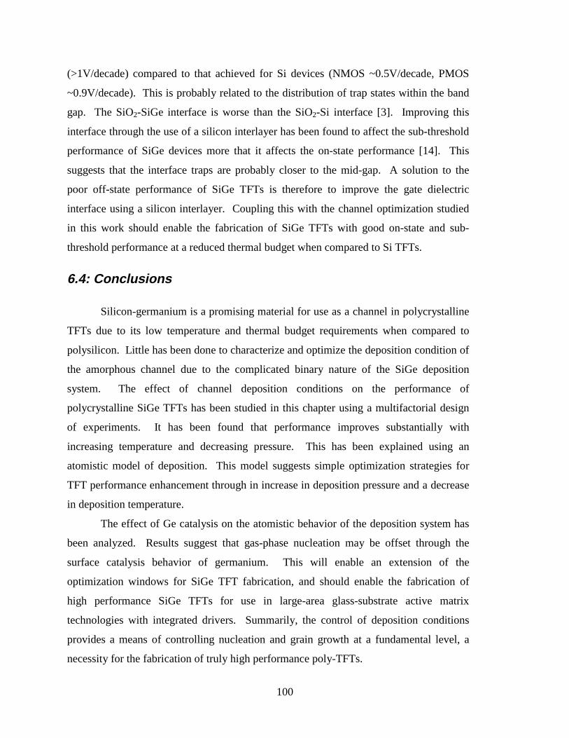
100
(>1V/decade) compared to that achieved for Si devices (NMOS ~0.5V/decade, PMOS
~0.9V/decade). This is probably related to the distribution of trap states within the band
gap. The SiO2-SiGe interface is worse than the SiO2-Si interface [3]. Improving this
interface through the use of a silicon interlayer has been found to affect the sub-threshold
performance of SiGe devices more that it affects the on-state performance [14]. This
suggests that the interface traps are probably closer to the mid-gap. A solution to the
poor off-state performance of SiGe TFTs is therefore to improve the gate dielectric
interface using a silicon interlayer. Coupling this with the channel optimization studied
in this work should enable the fabrication of SiGe TFTs with good on-state and sub-
threshold performance at a reduced thermal budget when compared to Si TFTs.
6.4: Conclusions
Silicon-germanium is a promising material for use as a channel in polycrystalline
TFTs due to its low temperature and thermal budget requirements when compared to
polysilicon. Little has been done to characterize and optimize the deposition condition of
the amorphous channel due to the complicated binary nature of the SiGe deposition
system. The effect of channel deposition conditions on the performance of
polycrystalline SiGe TFTs has been studied in this chapter using a multifactorial design
of experiments. It has been found that performance improves substantially with
increasing temperature and decreasing pressure. This has been explained using an
atomistic model of deposition. This model suggests simple optimization strategies for
TFT performance enhancement through in increase in deposition pressure and a decrease
in deposition temperature.
The effect of Ge catalysis on the atomistic behavior of the deposition system has
been analyzed. Results suggest that gas-phase nucleation may be offset through the
surface catalysis behavior of germanium. This will enable an extension of the
optimization windows for SiGe TFT fabrication, and should enable the fabrication of
high performance SiGe TFTs for use in large-area glass-substrate active matrix
technologies with integrated drivers. Summarily, the control of deposition conditions
provides a means of controlling nucleation and grain growth at a fundamental level, a
necessity for the fabrication of truly high performance poly-TFTs.

101
Chapter 7
Germanium-seeded laterally crystallized TFTs for
vertical integration of MOSFETs
___________________________________________
In chapter 5, the concept of lateral crystallization was introduced. Lateral
crystallization using patterned light absorption masks was demonstrated. This technique
demonstrates the power and flexibility of lateral crystallization as a means of fabricating
high-performance TFTs. Unfortunately, it is only usable for films deposited on
transparent substrates and hence cannot be used to achieve lateral crystallization of films
deposited on standard silicon substrates for such applications as vertical integration of
active devices. In this chapter, a technique to achieve lateral crystallization independent
of the substrate transparency is introduced. The technique utilizes the concept of seeding.
Seeded lateral solid-phase crystallization is not a new concept. Metal-induced
crystallization has been studied in the past, using such metals as nickel [1].
Unfortunately, the integration of such a process into a CMOS technology is problematic
due to the deleterious effect of nickel on device performance [2]. A metal-
contamination-free technique to achieve lateral crystallization could be integrated into a
standard CMOS process with significantly less difficulty. In this chapter, lateral
crystallization is demonstrated through the use of germanium seeding [3]. The technique
is free of metallic seeding agents, and therefore is easily integrated into a CMOS
technology. Additionally, the technique performs extremely well for small devices,
making it very promising for next generation VLSI applications. The actual process is
remarkably simple and is a batch process, and can therefore be used with a relatively
small increase in cost. The process has been used to fabricate high-performance TFTs
suitable for vertical integration applications. In this chapter, the conceptual basis for
germanium seeding is introduced. Then, the process for the fabrication of germanium-
seeded TFTs is detailed. Electrical results of device performance are presented and

102
analyzed. The applicability of germanium-seeded TFTs to vertical integration
applications is discussed.
7.1: Conceptual basis for germanium-seeding
The long incubation time associated with the amorphous to (poly)crystalline
transition is generally considered a disadvantage associated with low temperature SPC.
However, it can be exploited to achieve lateral crystallization. Nucleation can be
artificially induced in selected regions of the amorphous films using seeding agents.
These nuclei can then be enlarged while the rest of the film is still in the incubation stage,
making it possible to form abnormally large grains with controlled location. The laterally
crystallized grains cannot grow infinitely; after the passage of the incubation time,
homogenous nucleation will be induced in the rest of the film.
As introduced in chapter 6, silicon-germanium (SiGe) alloys exhibit a variation in
thermodynamic properties from those of silicon to those of germanium. This applies to
crystallization as well; silicon-germanium alloys crystallize much more rapidly than pure
silicon at a given temperature [4]. This fact has been used to reduce the incubation time
of amorphous silicon films for thin film transistors by replacing the amorphous silicon
with a bi-layer of SiGe and Si [5]. This same fact can also be used to enable the use of
germanium as a seeding agent for the lateral crystallization of amorphous silicon; the
germanium reacts with the Si to form a SiGe layer at the Ge-Si interface, which in turn
nucleates the lateral crystallization.
Volumetrically, the germanium needed to induce nucleation in silicon is quite
small. Given the exponential dependencies involved in nucleation and growth (as
discussed in chapter 2) and the reduction in thermal budget requirements caused by the
addition of germanium to silicon (as discussed in chapter 6), the formation of a small
amount of high Ge-fraction alloy at the interface is sufficient to cause nucleation.
Furthermore, Ge is not an excessively fast diffuser in Si, unlike typical metallic seeding
agents. Therefore, any effect of Ge is essentially confined to the Ge-Si interfacial region
and its surroundings.
These phenomena can be utilized to enable the germanium-seeded lateral
crystallization of amorphous silicon, used to fabricate high-performance TFTs.

103
7.2: Experimental details
To simulate the intended application of the devices, all devices in this study were
fabricated on oxidized silicon wafers. The overall process flow is shown below (Figure
7.1).
LTO
LTO
Deposit amorphous channel film
Deposit and pattern sacrificial oxide
Deposit germanium selectively
Crystallize at low temperature
Oxidized Silicon Substrate
a-Si
Germanium
Strip LTO, Ge and build TFT
Lateral crystallization Self-nucleation
Substrate
Channel
Gate
Source Drain
LTO
Gate Oxide
ALTERNATIVE: Single-sided Seed
GermaniumLTO
Figure 7.1: Process flow for Ge-seeded laterally crystallized TFT fabrication
100nm amorphous silicon was deposited by LPCVD at 500°C / 1000mtorr from
SiH4. These deposition conditions were chosen as they were previously identified as
resulting in films having a long nucleation incubation time. On these silicon films, 50nm
LPCVD (LTO) SiO2 was deposited for use as a sacrificial layer. Square seeding windows
of 1µm side were opened in this layer. The windows were positioned either over the
drain of the TFT structure or over both the source and drain of the same. Then, Ge was
deposited by LPCVD at 500°C/100mtorr from GeH4. Under these conditions, the Ge was
deposited as a polycrystalline material. The deposition of Ge from GeH4 is inherently
selective on Si vs. SiO2. Therefore, the Ge deposited only within the previously opened
seeding windows. Immediately after Ge deposition, the wafers were annealed in argon at
500°C-550°C to fully crystallize the channel films. For comparison, wafers without any
Ge seeding were crystallized simultaneously. After crystallization, the remaining Ge was

104
removed in H2SO4:H2O2, and the sacrificial oxide was removed in HF. Standard planar
top-gate self-aligned TFTs were then fabricated. 30nm thermal SiO2 was used as the gate
dielectric, and 250nm in-situ doped polysilicon was used as the gate electrode. Note the
high temperatures used in this process compared to those used in previous chapters.
These were used since the devices discussed here are intended for use in vertically
integrated circuits rather than displays, and hence do not have the glass-warpage
constraints of devices intended for AMLCD applications. Junctions were formed using
implantation of boron and phosphorus. No LDD or spacer technology was used. The
peak process temperature was 900°C. After device fabrication, electrical performance of
the TFTs was evaluated. Plan-view TEMs of the channel films were also made to
determine the seeding efficiency.
7.3: Results and discussion
To determine the extent of crystallization into the channel films, AFM images
were taken of defect-etched seeded films after a partial crystallization. As is evident
from the AFM image shown below (Figure 7.2), polycrystalline silicon is formed at the
seed point and is not etched as rapidly as the surrounding amorphous film, resulting in a
height differential. Focused EDAX of the same film indicates the presence of less than
1% Ge within the seeded regions and its total absence in the remaining Si.
Figure 7.2: AFM image showing polycrystalline seed points after defect etcha

105
A plan-view TEM of a further-annealed seeded region is shown below (Figure
7.3). It is evident from this figure that grains are formed in the seeded region and extend
into the still-amorphous matrix. Note that numerous grains may grow out of each seed
point, depending on the size of the point. These grains have numerous defects within
them. Some of these defects are annealed out during the subsequent high temperature
processing.
Figure 7.3: Plan-view TEM showing growth of seeded grains with seed structure
boundary overlaid in white
Electrical characteristics of 0.9µm/0.7µm NMOS and PMOS devices are shown
below (Figure 7.4 and Figure 7.5). It is evident that there is substantial improvement in
device performance. The seeded devices shown in these plots were seeded in both the
source and drain regions. To compare the performance of the seeded devices with the
unseeded devices, various device parameters were calculated and are summarized (Table
7-1). Clearly, the seeded devices are superior to the unseeded ones.
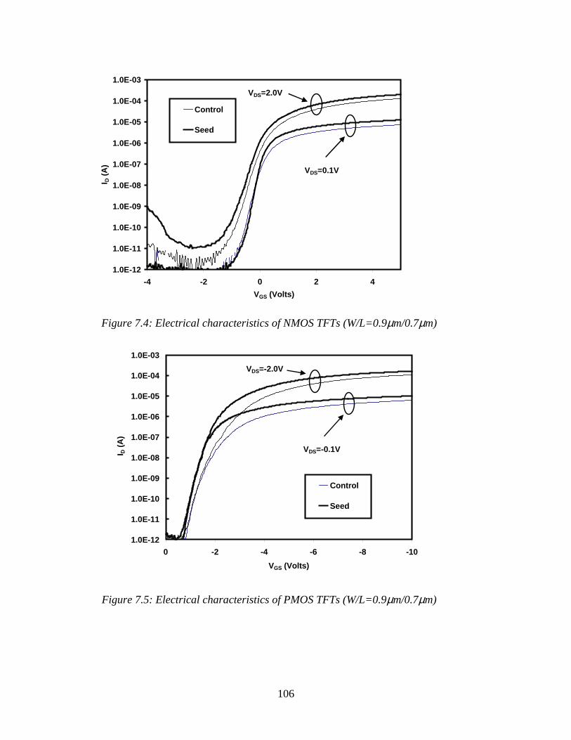
106
1.0E-12
1.0E-11
1.0E-10
1.0E-09
1.0E-08
1.0E-07
1.0E-06
1.0E-05
1.0E-04
1.0E-03
-4 -2 0 2 4
VGS (Volts)
I D (
A)
Control
Seed
VDS=0.1V
VDS=2.0V
Figure 7.4: Electrical characteristics of NMOS TFTs (W/L=0.9µm/0.7µm)
1.0E-12
1.0E-11
1.0E-10
1.0E-09
1.0E-08
1.0E-07
1.0E-06
1.0E-05
1.0E-04
1.0E-03
-10-8-6-4-20
VGS (Volts)
I D (
A)
Control
Seed
VDS=-0.1V
VDS=-2.0V
Figure 7.5: Electrical characteristics of PMOS TFTs (W/L=0.9µm/0.7µm)

107
Table 7-1: Summary of device characteristics (W/L=0.9µm/0.7µm)
Parameter NMOS PMOS
Unseeded Dual-seeded Unseeded Dual-seeded
Field-effect mobility
(cm2/V-s)
100 254 70 101
Sub-threshold slope
(V/dec.)
0.22 0.22 0.25 0.22
Leakage current
(pA/µm)
5 7 1 1
To determine the extent of lateral crystallization, the variation in mobility with
device dimensions was analyzed. The variation in NMOS mobility vs. channel length for
both dual-seeded (seeded in both the source and the drain) and single-seeded (seeded in
only the drain) devices vs. control devices is shown below (Figure 7.6). From this figure,
it is apparent that seeded devices perform better than unseeded devices in all cases. The
extent of improvement increases dramatically for smaller devices. For larger devices,
dual-seeded structures are superior. However, a crossover occurs, and single-seeded
devices are better at shorter channel lengths, for reasons discussed later.
0
50
100
150
200
250
300
350
0 2 4 6 8 10 12 14 16 18 20
Channel Length (µm)
Fie
ld-e
ffec
t M
ob
ility
(cm
2 /V-s
)
Unseeded
Single Seed
Dual Seed
Figure 7.6: Variation in NMOS field-effect mobility with channel length

108
The effect of overall device geometry on seeding efficiency was also analyzed.
The variation in NMOS mobility improvement is shown below (Figure 7.7) as a function
of both channel length and width. Note that the smallest devices show the most
improvement, as noted above. A crucial factor affecting the implementation of any
lateral crystallization technology is that of uniformity. The mobility distribution achieved
using the two seeding structures is contrasted to unseeded devices below (Table 7-2).
1 2 4 6 8 10 15 20
1
26
10
0
20
40
60
80
100
120
140
160
Improvement in µFE (%)
Channel Length (µm)
Channel Width (µm)
Figure 7.7: Variation in NMOS mobility improvement with device size
Table 7-2: Summary of intra-wafer mobility uniformity (W/L=0.9µm/0.7µm)
Process Mobility
(cm2/V-s)
Variation
(σ2)
Notes
Unseeded 100 40% Typical distribution
Dual-Seeded 254 20% Slightly lopsided
Single-Seeded 303 40% Extremely long tail
The efficiency of seeding is apparent (Figure 7.2); every seed point exhibits the
existence of polycrystalline material. These nucleated regions result in the formation of
109
laterally crystallized grains away from the seed point into the device channel. Different
orientations have different growth rates, and therefore, high growth rate orientations tend
to dominate. This leads to the prevalence of a majority of devices with essentially one
laterally crystallized grain extending into the channel from each seed point, resulting in
the relatively good uniformity seen for dual-seeded devices. Figure 7.8 shows the
distributions of field-effect mobility for unseeded and seeded NMOS devices.
0
1
2
3
4
5
6
7
8
50 70 90 110
130
150
170
190
210
230
250
270
290
310
330
350
Field-effect mobility, µFE (cm2/V-s)
Po
pu
lati
on
ControlDual SeedSingle Seed
Figure 7.8: NMOS mobility distributions for seeded and unseeded devices
The difference in performance and uniformity obtained from dual-seeded and
single-seeded devices is explained upon consideration of the effect of device geometry
upon performance. For large devices, the laterally crystallized region is a relatively small
fraction of the overall channel; typical laterally crystallized grains are approximately 1µm
long. Therefore, the resulting improvement in performance is marginal for larger
devices. Since the dual-seeded devices have two laterally crystallized regions, they
exhibit better performance than the single-seeded devices, which have only one laterally
crystallized region. As the channel length and width are reduced, the laterally
crystallized region becomes a larger fraction of the overall device. This is shown

110
schematically below (Figure 7.9). For extremely small devices, the channel becomes
almost a single grain (for the single-seeded devices) or two grains (for the dual-seeded
structures). This results in the crossover in performance noted in previously.
Small Device
Seeded device show greatimprovement
Large Device
Seeded devices show little improvement
SeedPoint
SeedPoint
Laterallycrystallized grain
is small fraction ofchannel
Laterallycrystallized grainis large fraction of
channel
Figure 7.9: Schematic view of lateral crystallization in the device channel
The uniformity of dual-seeded small devices is better than unseeded devices
because the two seeded grains impinge to form a two-grain structure in the majority of
devices. This is because the overall laterally crystallized region can extend as much as
2µm, due to the summation of the two grains, and is therefore much larger than the
channel dimensions. In single-seeded devices, on the other hand, the grain size is the
same or less than the device size (upon inclusion of the separation of the seed point from
the channel, approximately 1µm). Therefore, though performance is improved in many
devices, uniformity is poor due to the statistical variations in the extent of lateral
crystallization. This also explains the one-sided population distribution noted previously.
Based on the results and analysis detailed above, it is apparent that excellent
performance can be obtained using this technology, through the elimination of grain
boundaries from within the channel of the devices. However, as is apparent from the
TEM image (Figure 7.3), several intra-grain defects are still in existence. These degrade
the device performance to below that of bulk devices and result in the poor sub-threshold
slope noted.
To develop this technology to its full potential, it will be necessary to reduce the
number of intra-grain defects within the channel. One way of achieving this is through
111
the replacement of silane with disilane, allowing for more optimized low temperature,
high deposition rate (and therefore more amorphous) films. This will result in a lower
density of defects through a reduction in the nucleation rate, and also in an increased
average grain size [6]. The increase in average grain size will result in improved
uniformity for smaller devices. Furthermore, the use of this technology in deep-
submicron devices, as mandated by VLSI, should enable the fabrication of extremely
high performance devices offering good uniformity.
The overall thermal budget used in the crystallization process is low. The
maximum temperature excursion is 550°C, excluding the gate oxidation step.
Replacement of this thermal oxide dielectric with a high quality deposited dielectric will
further reduce the thermal budget, making the process fully compatible with the bulk
devices existing on lower levels in a vertically integrated circuit. The use of advanced
plug technologies should enable the interconnection of these devices, resulting in the
development of a vertically integrated, high performance CMOS technology for next-
generation giga-scale integration applications.
7.4: Conclusions
In this chapter, a novel technique to fabricate high-performance laterally
crystallized thin film transistors has been described. Germanium seeding is used to
nucleate the lateral crystallization of amorphous silicon films using a low thermal budget,
CMOS-compatible process. The resulting film is used as the channel film for the
fabrication of high-performance TFTs. The seeding technique excels at short channel
lengths, making it extremely promising as a means of fabricating devices offering near-
single-crystal performance on insulating layers. Therefore, the technique can be used to
enable the vertical integration of CMOS devices for 3-D VLSI applications.
Experimental results show that the technique can be used in the fabrication of
essentially single-grain transistors. Extension of the technology using advanced
deposition processes and deep-submicron devices should enable the development of a
technology for the manufacture of high performance TFTs for vertically integrated circuit
applications, enabling higher chip speeds through reduced interconnect delays and
substantially increased packing densities.

112

113
Chapter 8
Conclusions
___________________________________________
In this work, the control of nucleation and grain growth has been studied as a
means of forming high-quality polycrystalline silicon. Various techniques to achieve this
control have been investigated and demonstrated. Using these techniques, high-
performance TFTs have been fabricated with applications in flat panel displays and the
vertical integration of active devices for VLSI applications. Two techniques to fabricate
spatially-specified large grain polysilicon have been demonstrated for the first time.
Additionally, a novel acoustic crystallinity and temperature sensor has been demonstrated
and characterized as part of this work.
8.1: Summary
Amorphous silicon can be deposited by LPCVD and subsequently crystallized in
the solid phase to form large grain polysilicon for use in the fabrication of thin film
transistors. Crystallization occurs through a process of nucleation and subsequent grain
growth. Both these processes have characteristic activation energies which can be
explained upon consideration of atomistic attachment phenomena. The precise values of
these activation energies are functions of the crystallization conditions and the deposition
conditions of the amorphous film.
Since nucleation and grain growth are essentially independent and competitive
processes, the potential exists for the modification of their relative rates to alter the
quality of the final polysilicon film. This may be done thermally by altering the
annealing temperature conditions over time to change the relative rates of nucleation and
grain growth. The thermal exposure may be varied spatially as well, by using selective
heating techniques. The rate modification may also be achieved artificially by changing
the activation energies through a material interaction.

114
In this work, the theory and implementation of such crystallization control
processes have been studied extensively. These processes have been used to fabricate
high-performance thin film devices for display and vertical integration applications. The
results of these investigations are summarized below.
8.1.1: Theory of deposition and solid phase crystallization
The deposition of silicon has been studied extensively in the past. Most of this
work has concentrated on epitaxy and the deposition of polycrystalline silicon. Some
analysis of the deposition of amorphous silicon has also been performed, though less
detail. Using an analysis of atomistic attachment processes, the kinetics of the deposition
of amorphous silicon have been analyzed. Combining gas phase and surface processes, a
methodology for estimating the quality of an amorphous film based on its deposition
conditions has been developed. The effect of the initial stages of deposition has been
studied in particular. These results have been used to explain the various experimental
results reported in the literature.
The solid-phase crystallization of amorphous silicon has also been studied.
Performing an analysis of the attachment kinetics at the crystalline-amorphous interface,
the kinetics of solid-phase crystallization have been analyzed. These results have been
combined with the aforementioned deposition analysis to develop a unified model of the
low-pressure chemical vapor deposition and subsequent solid-phase crystallization of
amorphous silicon. The mechanisms of defect formation during solid-phase
crystallization have also been reviewed.
8.1.2: Detection of nucleation and crystallization in amorphous silicon
To aid in the experimental demonstration of the theory developed above, an
acoustic crystallinity and temperature sensor has been developed. An existing acoustic
temperature sensor has been utilized to detect crystallinity by exploiting the heat
absorption changes induced in films deposited on transparent substrates during the
amorphous to crystalline transition. The sensor has been extensively characterized. It
has been found that the sensor is sensitive enough to detect nucleation-type events.

115
Therefore, the sensor may be used in experiments to demonstrate the concepts developed
above.
8.1.3: Experimental demonstration of controlled nucleation and growth
The bulk of this work has been dedicated to the development of various
technologies that exploit the control of nucleation and grain growth to enable the
fabrication of high-performance thin film transistors. These technologies, besides being
useful in themselves, act as demonstrations of the theoretical concepts developed in the
initial sections of this work.
• Two-step annealing for process throughput improvement - the first
experimental demonstration of concept was a logical extension to the
experiments performed to characterize the acoustic crystallinity sensor. Since
the sensor enables the detection of nucleation, it was possible to improve
throughput by rapidly nucleating a film at elevated temperature, using the
sensor for end-point detection. Since a large fraction of the overall
crystallization time consists of the incubation time prior to nucleation, this
resulted in a substantial improvement in process throughput. Thus, using the
two-step annealing process, nucleation was initially enhanced (at high
temperature) to short-circuit the incubation stage and subsequently retarded
(at low temperature) to ensure formation of large grains. Indeed, the rapid
temperature-quench actually resulted in an enhancement in average grain size.
• Lateral crystallization using patterned light absorption masks - since the
above experiment was inherently limited in scope by the fact that nucleation
occurred randomly throughout the film, the next logical step was to attempt to
spatially control nucleation. This was achieved thermally using light
absorption masks to increase heating in specific regions of the film. These
regions nucleated first, and were subsequently grown laterally to form large-
grain spatially-specified polysilicon. By placing the nucleation regions at the
electrodes of a TFT and crystallizing into the channel, it was possible to
fabricate TFTs having extremely high-performance. This technique thus
explored the concept of lateral crystallization achieved through spatial control

116
of nucleation. The technique also allows for the tuning of device performance
on a single substrate by changing the structure of the absorption mask.
• Optimization of amorphous precursor characteristics of SiGe alloys - all the
experiments summarized above attempt to enhance performance by
controlling the crystallization processes. From the theory developed in this
work, such control should also be possible by changing the deposition
conditions of the amorphous film. Experiments were performed using silicon-
germanium films. These were chosen since they are extremely promising for
flat panel display applications due to their low thermal budget requirements.
Additionally, they provide a demonstration vehicle for various surface
attachment phenomena. Experiments were performed to determine the effect
of deposition temperature and pressure on final device performance. It was
determined that the experimental results matched theoretical expectations
extremely well. These results indicate that the theory developed in this work
may be used to optimize the characteristics of silicon-germanium TFTs for
display applications. Additionally, gas-phase and surface reactivity
phenomena were used to explore and model the optimization boundaries
during deposition. These results were also found to agree with theoretical
expectations.
• Germanium-seeded laterally crystallized TFTs - since silicon-germanium
alloys have lower thermal budget requirements than silicon during
crystallization, it is possible to spatially alter nucleation rates using selectively
located germanium islands. The silicon-germanium alloy forms at the
interface of the silicon and germanium. This nucleates first and can then be
grown out laterally to form large-grain spatially-specified polysilicon. Again,
by placing these islands at the terminals of TFTs, it is possible to achieve
lateral crystallization into the channel. In fact, using this technique, the
potential exists for the fabrication of single-grain TFTs. Devices having on-
state performance approaching that of bulk devices have been demonstrated.
117
This last experiment is a fitting final demonstration of the concepts developed in
this work. With further optimization, it may be possible to fabricate single-grain devices,
making the possibility of high-performance displays with integrated drivers and vertically
integrated VLSI circuits a reality. All this is possible through the control of nucleation
and grain growth during solid-phase crystallization of silicon.
8.2: Recommendations for future work
This work explores and demonstrates concepts in solid phase crystallization and
its control. To enable the realization of the full potential of the technologies explored
here, further research is needed in the following areas:
• Unification of the models of deposition crystallization -- a complete
quantitative unification of the models of deposition and crystallization is
required to enable proper optimization of deposition and crystallization
conditions. In particular, further experimental and theoretical work is required
to study the effects of the initial stages of deposition. As identified in this
work, this stage of growth has a critical effect on final film quality and
therefore, the study of this stage is vital. Further research on the electrical
behavior of the various defects in polysilicon is also highly desirable.
• The acoustic crystallinity sensor and throughput reduction -- the
characterization of the sensor is fairly complete; however, further work is
required on the sensor implementation. Integration of the sensor into a
closed-loop control system is crucial if it is to be used for nucleation detection
during two-step annealing. Further research is required into the two-step
anneal process itself to determine the optimal time point for the quench. This
should enable further improvements in both process throughput and device
performance.
• Patterned light absorption masking -- this technique, as currently
implemented, is not truly glass-compatible. To achieve glass compatibility,
implementation of this technique must be performed using scanned rapid
thermal annealing. The use of more absorbent materials as the absorption
masks is also in need of investigation. Quantitative theoretical and

118
experimental work is required to model the absorption masking process,
enabling proper optimization of the technology.
• Germanium seeding -- the current limits of this technique are imposed by
homogenous nucleation within the silicon film itself. Therefore, substantial
work is required to minimize the required grain size relative to the incubation
time. The use of disilane as a silicon source is in need of investigation to
enable an increase in average homogenous grain size, indicative of an
increased grain growth to nucleation ratio. This will allow the use of faster
crystallization anneals. Additionally, the devices must be scaled to sub-
micron dimensions to exploit the full capabilities of this technology.

119
Appendix 1
The Effect of Defects on Electron Transport in
Polycrystalline Silicon-based Devices
___________________________________________
In chapter 2, the theoretical basis for the formation of polycrystalline silicon was
discussed. Theory was developed that explained the formation and spatial distribution of
grain boundaries. In several subsequent chapters, the implications of the control of grain
boundary distribution on device performance were experimentally demonstrated.
Intuitively, a reduction in grain boundary population density would be expected to
improve device performance. However, some physical explanation of this is also
desirable. Therefore, in this appendix, the effect of grain boundary defects on electron
transport in polycrystalline silicon semiconductor devices is briefly reviewed. The basic
theoretical explanations of electron transport across grain boundaries are first introduced.
Then, the extension of these models to explain conduction in thin film transistors is
briefly developed. Thus, a physical explanation of the phenomenon exploited throughout
this work is provided.
A1.1: A model of electron trapping in grain boundaries
Several authors have studied the trapping of carriers in grain boundaries [1, 2, 3].
In general, for simplicity of analysis, polysilicon is assumed to be composed of a linear
chain of identical crystallites having a grain size, L. The grain boundary thickness is
assumed to be negligible compared to L. The grain boundaries are assumed to contain a
concentration of traps Nt, located at energy Et with respect to the intrinsic Fermi level.
The traps are assumed to be initially neutral and become charged by trapping a carrier.
Using an abrupt depletion approximation, a simplified band structure of polycrystalline
silicon can be developed. This is shown below (Figure A1. 1).

120
Crystallite
EF
EC
Ei
EV
EB
Grain Boundary
Q
Figure A1. 1: Grain structure, charge distribution and band diagram assumed in grain
boundary trapping model
Transport properties are calculated in one dimension by assuming that the current
is governed by thermionic emission above the grain boundary barrier. The current
density across the barrier is therefore [1]:
−
= kT
EVkT
vnqJ B
dc exp0
2
Equation A1-5
where:
J is the current density
n0 is the concentration of free carriers in the grain
EB is the barrier height
Vd is the voltage drop across the grain
νc is a thermal collection velocity defined by:
121
2
1
*2
=
m
kTvc π
Equation A1-6
with m* being the effective mass of the carriers.
The conductivity described by thermionic emission above the grain boundary
barrier is therefore [1]:
−
=kT
Eqn Bexp00µσ
Equation A1-7
where:
µ0 is a mobility term describing barrier scattering:
kT
qLvc=0µ
Equation A1-8
Some carrier scattering is introduced by the grain boundary barrier itself, resulting
in the mobility term in the above equation. If additional scattering mechanisms are
allowed at the grain boundaries, then the mobility term can be modified as:
sb µµµ111
0
+=
Equation A1-9
where:
µs accounts for additional scattering terms.
The mobility in a single grain is therefore given by [4]:
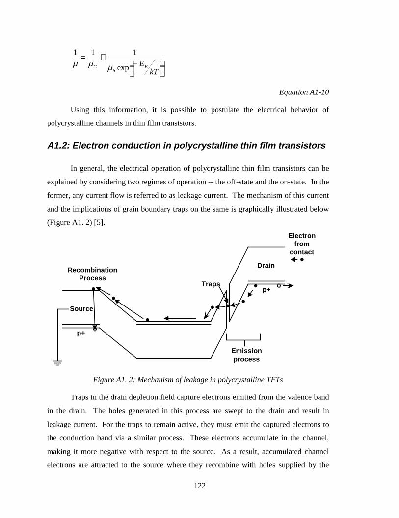
122
−+=
kTEB
bG exp
111
µµµ
Equation A1-10
Using this information, it is possible to postulate the electrical behavior of
polycrystalline channels in thin film transistors.
A1.2: Electron conduction in polycrystalline thin film transistors
In general, the electrical operation of polycrystalline thin film transistors can be
explained by considering two regimes of operation -- the off-state and the on-state. In the
former, any current flow is referred to as leakage current. The mechanism of this current
and the implications of grain boundary traps on the same is graphically illustrated below
(Figure A1. 2) [5].
p+
p+Traps
Emissionprocess
Electronfrom
contact
Drain
Source
RecombinationProcess
Figure A1. 2: Mechanism of leakage in polycrystalline TFTs
Traps in the drain depletion field capture electrons emitted from the valence band
in the drain. The holes generated in this process are swept to the drain and result in
leakage current. For the traps to remain active, they must emit the captured electrons to
the conduction band via a similar process. These electrons accumulate in the channel,
making it more negative with respect to the source. As a result, accumulated channel
electrons are attracted to the source where they recombine with holes supplied by the

123
ground. This process continues, resulting in experimentally observable device leakage.
The actual emission process may involve thermionic emission, thermionic field emission,
tunneling, or some combination of the three. By using the simple thermionic emission
theory developed in the previous section, the leakage current can be written as [4]:
−
=kT
El
VwtqNI BDbDL expµ
where:
VD is the drain-source voltage
w is the channel width
l is the channel length
The assumption inherent in this equation is that the mobility within the grain is
substantially greater than the grain boundary mobility, hence the use of µb. Using a
similar analysis, the on-state performance can be analyzed. Application of a gate voltage
of the appropriate polarity will cause a charge influencing both the barrier height and the
source-drain current. For an intrinsic channel device, the source-drain current can be
written as [4]:
∈
=G
ctG
DbD kTN
LNqN
l
VwqI
8exp
22
µ
where:
NG is the gate-induced charge concentration per unit area
The implications of these equations are as follows:
1. An increase in the density of grain boundaries will tend to increase leakage
current through an increase in trapping sites.
2. An increase in the density of grain boundaries will tend to decrease on-state
current through a reduction in channel mobility.
3. In particular, grain boundaries in the drain field will have a substantial impact
on off-state performance. The same will be true for any other trapping sites
present in the drain field.

124
4. Any other types of scattering sites will also tend to degrade on-state
performance.
Thus, through this analysis, the physical nature of conduction in polycrystalline
devices is apparent. Clearly, the key to performance improvement is a reduction in grain
boundary and other trap densities. In fact, this is the goal of this work and hence, the
physical justification for this work has been obtained.

125
Appendix 2
Thin Film Transistor Fabrication Processes
___________________________________________
Throughout this work, polycrystalline thin film transistors are used as the
demonstration vehicle for various crystallization concepts. Electrical behavior of TFTs is
used as a measure of the efficacy of the crystallization technique in question. To ensure
true comparison, a baseline TFT process was first developed. Two variations of this
process have been used in this work - a low temperature process for devices intended for
display applications, and a high temperature process for devices intended for vertically-
integrated VLSI applications. In this appendix, the process for the low temperature
fabrication of TFTs is explained in some detail. Then, the low-temperature and high-
temperature processes are contrasted. Thus, a comprehensive explanation of the device
fabrication processes used throughout this work is provided.
A2.1: Low-temperature TFT fabrication process
The low-temperature process used in this work was developed to enable the
fabrication of glass-compatible TFTs for AMLCD applications. Thus, to prevent glass
warpage, the maximum process temperature was limited to 600°C. The process begins
with the deposition of the channel film on an oxidized silicon or fused silica substrate.
This channel film is then crystallized using one of the techniques described in this work.
At this point, the sample consists of a blanket polycrystalline film on the insulating
substrate. Figure A2. 1 provides a cross-section of the sample at this point in the process.
Substrate
Channel Film
Figure A2. 1: Cross-section of wafer after channel deposition and crystallization

126
Next, the channel film is patterned and etched using an anisotropic polysilicon
etch, performed using SF6 and C2H5Cl. Figure A2. 2 shows the device cross-section at
this point.
Substrate
Channel Island
Figure A2. 2: Cross-section of device after active island patterning
Next, a gate oxide is deposited at 450°C by LPCVD from SiH4 and O2, and
annealed at 550-600°C. Figure A2. 3 shows the device cross-section at this point.
Substrate
ChannelGate Oxide
Figure A2. 3: Cross-section of device after gate oxide deposition
Next, the gate electrode is deposited by LPCVD. Typically, Si0.6Ge0.4 is used due
to its high deposition rate at low temperature (500°C). Figure A2. 4 shows the device
cross-section at this point in the process.
Gate Polysilicon
Substrate
ChannelGate Oxide
Figure A2. 4: Cross-section of device after gate electrode deposition
After gate deposition, the gate electrode is patterned using an anisotropic silicon
etch (Figure A2. 5).
Substrate
Channel
Gate
Gate Oxide
Figure A2. 5: Cross-section of device after gate patterning
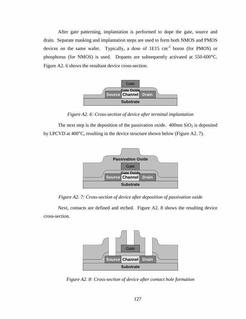
127
After gate patterning, implantation is performed to dope the gate, source and
drain. Separate masking and implantation steps are used to form both NMOS and PMOS
devices on the same wafer. Typically, a dose of 1E15 cm-2 boron (for PMOS) or
phosphorus (for NMOS) is used. Dopants are subsequently activated at 550-600°C.
Figure A2. 6 shows the resultant device cross-section.
Substrate
Channel
Gate
Source DrainGate Oxide
Figure A2. 6: Cross-section of device after terminal implantation
The next step is the deposition of the passivation oxide. 400nm SiO2 is deposited
by LPCVD at 400°C, resulting in the device structure shown below (Figure A2. 7).
Passivation Oxide
Substrate
Channel
Gate
Source DrainGate Oxide
Figure A2. 7: Cross-section of device after deposition of passivation oxide
Next, contacts are defined and etched. Figure A2. 8 shows the resulting device
cross-section.
Substrate
Channel
Gate
Source Drain
Figure A2. 8: Cross-section of device after contact hole formation

128
After contact hole formation, 1µm Al is deposited by sputtering, resulting in the
structure below (Figure A2. 9).
Aluminum
Substrate
Channel
Gate
Source Drain
Figure A2. 9: Cross-section of device after metal deposition
The final lithographic step is the patterning of the metal. The patterned metal is
typically wet-etched to form the finished device structure (Figure A2. 10).
Substrate
Channel
Gate
Source Drain
Figure A2. 10: Cross-section of finished device
At this point, the wafers are subjected to a forming gas anneal to 400°C, followed
by plasma hydrogenation at 300°C in a parallel plate hydrogen plasma. This is the final
step in the low-temperature TFT process.
A2.2: Differences between low- and high- temperature processes
The low-temperature process described in the previous section is intended for use
in applications requiring compatibility with glass substrates. To achieve this, several
design compromises were made. These result in a degradation in electrical performance

129
of the finished devices. If glass compatibility is not required, then some of these
compromises can be avoided, resulting in an improvement in baseline device
performance. The steps that are different in the high-temperature process are:
1. Gate dielectric - High temperature devices have a 30nm thermal oxide gate dielectric
with a high temperature (900°C) oxide anneal
2. Dopant activation - High temperature devices undergo dopant activation at 800°C,
resulting on more complete dopant activation
Through the use of these steps, high-temperature devices achieve a higher gate
oxide quality and lower series resistance. The high temperature steps also result in some
annealing of the polycrystalline channel film itself.

130

131
Bibliography
___________________________________________
Chapter 1
[1] J. E. Lilienfeld, US Patent 1 900 018, 1993.
[2] O Heil, British Patent 439 457, 1935 (German Patent date 1934).
[3] W. Shockley, “The path to the conception of the junction transistor”, IEEE. Trans.
Electron. Dev., vol. ED-23, pp. 597, 1976.
[4] J. S. Kilby, “Invention of the integrated circuit”, IEE. Trans. Electron. Dev., vol. ED-
23, pp. 648. 1976.
[5] D. Kahng and M. M. Atalla, “Silicon-silicon dioxide field induced surface devices”,
presented at IRE-AIEE Solid State Dev. Res. Conf., Pittsburgh, PA, 1960.
[6] P. K. Weimer, “The TFT - A new thin-film transistor”, Proc. IRE, vol. 50, pp. 1462,
1962.
[7] T. P. Brody, “The thin film transistor - A late flowering bloom”, IEEE Trans.
Electron. Dev., vol. ED-31, pp. 1614, 1984.
[8] P. K. Weimer, “Systems and technologies for solid-state image sensors”, RCA Rev.,
vol. 32, pp. 251, 1971.
[9] P. K. Weimer, US Patent 3 191 061, 1965.
[10] T. P. Brody and D. J. Page, “Flexible transistors, large-scale integration and
displays”, Government Microcircuit Applications Conf. Dig., pp. 92, 1969.
[11] B. J. Lechner et al, “Liquid crystal matrix displays”, Proc. IEEE, vol. 59, pp. 1566,
1971.
[12] S. Jurichich, S. C. Wood, and K. C. Saraswat, “Cost modelling of low-temperature
large-area polysilicon thin film transistor liquid crystal display manufacturing”, Proc.
SPIE, vol. 3014, pp. 160, 1997.

132
[13] H. Maeda, K. Fujii, N. Yamagishi, H. Fujita, S. Ishihara, K. Adachi, and E. Takeda,
“A 15-in. full-color high-resolution TFT-LCD”, Society for Information Display Intl.
Symp. Dig. Technical Papers., vol. 23, pp. 47, 1992.
[14] P. Alt and P. Pleshko, “Scanning limitations of liquid-crystal displays”, IEEE Trans.
Electron. Dev., vol. ED-21, pp. 146, 1974.
[15] E. Kaneko, Liquid crystal TV displays applications of liquid crystal displays. D.
Reidel, Boston, 1987.
[16] M. Anma and F. Okamoto, “Compaction of glass substrates for active-matrix
LCDs”, Society for Information Display Intl. Symp. Dig. Technical Papers, vol. 24, pp.
971, 1993.
[17] T. Ohm, T. Hoshi, T. Yoshie, T. Takewaki, M. Otsuki, T. Shibata, T. Nitta, “Large-
electromigration-resistance copper interconnect technology for sub-half-micron ULSI’s”,
IEEE International Electron. Dev. Meeting Tech. Dig., pp. 285, 1991.
[18] H. Igarashi, H. Oyamatsu, M. Kodera, N. Kaji, T. Matsuno, I. Shibata, M.
Kinugawa, M. Kakumu, “Manufacturable and reliable fluorine-doped low-k interlayer
dielectric process for high performance logic LSI”, 1996 Symposium on VLSI Technology
Digest of Technical Papers, pp. 85, 1996.
[19] T. Yamanaka, T. Hashimoto, N. Hasegawa, T. Tanaka, N. Hashimoto, A. Shimizu,
N. Ohki, K. Ishibashi, K. Sasaki, T. Nishida, T. Mine, E. Takeda, T. Nagano, “Advanced
TFT SRAM technology using phase-shift lithography”, IEEE Trans. Electron. Dev., vol.
42, pp. 1305, 1995.
[20] T. Noguchi, “Appearance of single-crystalline properties in fine-patterned Si thin
film transistors (TFTs) by solid phase crystallization (SPC)”, Jap. J. Appl. Phys. Part 2
(Letters), vol. 32, pp. L1584, 1993.
[21] I-W. Wu, “Polycrystalline silicon thin film transistors for liquid crystal displays.”,
Solid State Phenomena, vol. 37-38, pp. 553, 1194.
[22] K. Sera, F. Okumura, H. Uchida, S. Itoh, S. Kaneko, and K. Hotta, “High-
performance TFT’s fabricated by XeCl excimer laser annealing of hydrogenated
amorphous silicon film.”, IEEE Trans. Electron Dev., vol. 106, pp. 2868, 1989.

133
[23] D. N. Kouvatsos, A. T. Voutsas, and M. K. Hatalis, “High-performance thin-film
transistors in large grain size polysilicon deposited by thermal decomposition of
disilane”, IEEE Trans. Electron Dev., vol. 43, pp. 1399, 1996.
[24] M. Bonnel, N. Duhamel, M. Guendouz, L. Haji, B. Loisel, and P. Ruault, “Poly-Si
thin film transistors fabricated with rapid thermal annealed silicon films.”, Jpn. J. Appl.
Phys., vol. 30, pp. L1924, 1991
Chapter 2
[1] V.dela Torre, J. Foerstner, B. Lojek, K. Sakamoto, S. L. Sundaram, N. Tracht, B.
Vasquez, and P. Zdebel, “MOSAIC V - A very high performance bipolar technology”,
Proc. 1991 IEEE Bipolar Circuits and Technology Meeting, pp. 21, 1991.
[2] T. I. Kamins and S-Y. Chiang, “CMOS device isolation using the selective-etch-and-
refill-with-EPI (SEREPI) process”, IEEE Electron Dev. Lett., vol. EDL-6, pp. 617, 1985.
[3] S. S. Wong, D. R. Bradbury, D. C. Chen, and K. Y. Chiu, “Elevated source / drain
MOSFET”, IEDM Technical Digest, pp. 634, 1984.
[4] R. H. Dennard, F. H. Gaensslen, H-N. Yu, V. L. Rideout, E. Bassous, and A.
LeBlanc, “Design of ion-implanted MOSFET’s with very small physical dimensions”,
IEEE J. Solid-State Circuits, vol. SC-9, pp. 256, 1974.
[5] T. Shiba, T. Uchino, K. Ohnishi, and Y. Tamaki, “In situ phosphorus-doped
polysilicon emitter technology for very high-speed small emitter bipolar transistors”,
IEEE Trans. Electron. Dev., vol. 43, pp. 889, 1996.
[6] N. Ibaraki, “a-Si TFT technologies for AMLCDs”, in Flat Panel Display Materials,
Editor: J. Batey, Mat. Res. Soc. Symp. Proc., pp. 3, 1994.
[7] T. Yoshida, Y. Ichikawa, and H. Sakai, “Amorphous silicon solar cell technologies”,
Optoelectronics - Devices and Technologies, vol. 9, pp. 577, 1994.
[8] T. Morita, S. Tsuchimoto, and N. Hashizume, “The low temperature polysilicon TFT
technology for manufacturing of active matrix liquid crystal displays”, in Flat Panel
Display Materials, Editor: J. Batey, Mat. Res. Soc. Symp. Proc., pp. 71, 1994.

134
[9] G. Harbeke, L. Krausbauer, E. F. Steigmeier, A. E. Widmer, H. F. Kappert, and G.
Neugebauer, “Growth and physicl properties of LPCVD polycrystalline silicon films”, J.
Electrochem. Soc., vol. 131, pp. 675, 1984.
[10] M. K. Hatalis and D. W. Greve, “Large grain polysilicon by low-temperature
annealing of low-pressure chemical vapor deposited amorphous silicon films”, J. Appl.
Phys., vol. 63, pp. 2260, 1988.
[11] M. Bonnel, N. Duhamel, M. Guendouz, L. Haji, B. Loisel and P. Ruault, “Poly-Si
thin-film transistors fabricated with rapid thermal-annealed silicon films” ̧Jpn. J. Appl.
Phys., vol. 30, no. 11B, pp. L1924, 1991.
[12] K. Shimuz, O. Sugiura, and M. Matsumura, “On-chip bottom-gate polysilicon and
amorphous silicon thin-film transistors using excimer laser annealing”, Jpn. J. Appl.
Phys., vol. 29, pp. L1775, 1990.
[13] D. W. Greve and M. Racanelli, “Growth rate of doped and undoped silicon by ultra-
high vacuum chemical vapor deposition”, J. Electrochem. Soc., vol. 138, pp. 1744, 1991.
[14] A. T. Voutsas and M. K. Hatalis, “Structure of as-deposited LPCVD silicon films at
low deposition temperatures and pressures”, J. Electrochem. Soc., vol. 139, pp. 2659,
1992.
[15] I-M R. Lee, G. W. Neudeck, and C. G. Takoudis, “Low pressure chemical vapor
deposition of epitaxial silicon-germanium, epitaxial silicon and poly-silicon”, CVD XIII
Proceedings of the thirteenth international conference on chemical vapor deposition,
1996, pp. 107-112.
[16] M. McEllistrem, M. Allgeier, and J. J. Boland, “Dangling bond dynamics on the
silicon (100) - 2 × 1 surface: dissociation, diffusion, and recombination”, Science, vol.
279, pp. 545, 1998.
[17] W. A. Tiller, The Science of Crystallization : Microscopic Interfacial Phenomena,
Cambridge University Press, pp. 176. 1991.
[18] J. Bloem, “Nucleation and growth of silicon by CVD”, J. Cryst. Growth, vol. 50, pp.
581-604, 1980.
[19] J. Bloem and L. J. Giling, “Epitaxial growth of silicon by chemical vapor
deposition”, VLSI Electronics Microstructure Science, vol. 12, pp. 89-139, 1985.
135
[20] K. D. Brodska and C. Kleint, Thin Solid Films, vol. 34, pp. 131, 1976.
[21] V. Subramanian and K. C. Saraswat, “Optimization of Silicon-Germanium TFTs
through the control of amorphous precursor characteristics”, submitted to IEEE Trans.
Electron Dev., 1997
[22] G. M. Barrow, Physical Chemistry, 5th Ed., McGraw-Hill, New York, pp. 708.,
1988.
[23] K. F. Kelton, A. L. Greer, and C. V. Thompson, “Transient nucleation in consensed
systems”, J. Chem. Phys., vol. 79, pp. 6261, 1983.
[24] R. B. Iverson and R. Reif, “Recrystallization of amorphized polycrystalline silicon
films on SiO2: Temperature dependence of the crystallization parameters”, J. Appl. Phys.,
vol. 62, pp. 1675, 1987.
[25] D. Kashchiev, “Solution of the non-steady state problem in nucleation kinetics”,
Surface Science, vol. 14, pp. 209, 1969.
[26] K. Zellama, P. Germain, S. Squelard and J. C. Bourgoin, “Crystallization in
amorphous silicon”, J. Appl. Phys., vol 50, pp. 6995-7000, 1979.
[27] U. Koster, “Crystallization of amorphous silicon films”, Phys. Status Solidi A, vol.
48, pp. 313, 1978.
[28] N. A. Blum and C. Feldman, “The crystallization of amorphous silicon films”, J.
Non-Cryst. Solids, vol. 11, pp. 242, 1972.
[29] L. Csepregi, E. F. Kennedy, and J. W. Mayer, “Substrate-orientation dependence of
the epitaxial reogrowth rate from Si-implanted amorphous Si”, J. Appl. Phys., vol. 49, pp.
3906, 1978.
[30] M. Avrami, “Kinetics of Phase Change. I”, J. Chem. Phys., vol. 7, pp. 1103, 1939.
[31] M. Avrami, “Kinetics of Phase Change. II”, J. Chem. Phys., vol. 8, pp. 212, 1939.
[32] M. Avrami, “Kinetics of Phase Change. I”, J. Chem. Phys., vol. 9, pp. 177, 1939.
[33] K. Nakazawa, “Recrystallization of amorphous silicon films deposited by low-
pressure chemical vapor deposition from Si2H6 gas”, J. Appl. Phys., vol. 69, pp. 1703,
1991.

136
[34] T. Aoyama, G. Kawachi, N. Konishi, T. Suzuki, Y. Okajima, and K. Miyaoto,
“Crystallization of LPCVD silicon films by low temperature annealing”, J. Electrochem.
Soc., vol. 136, pp. 1169, 1989.
[35] E. M. Pearson, T. Halicioglu, and W. A. Tiller, “Adatom diffusion and adatom-ledge
interaction on the Si(111) surface using a semiempirical potential energy function”, J.
Crystal Growth, vol. 83, pp. 499, 1987.
[36] G. Brocks, P. J. Kelly,and R. Car, “Binding and diffusion of a Si adatom on the
Si(100) surface”, Phys. Rev. Lett., vol. 66, pp. 1729, 1991.
[37] D. Srivastava and B. J. Garrison, “The dynamics of surface rearrangements in Si
adatom diffusion on the Si(100)(2*1) surface”, J. Chem. Phys., vol. 95, pp. 6885, 1991.
[38] M. E. Keeffe, C. C. Umbach, and J. M. Blakely, “Surface self-diffusion on Si from
the evolution of periodic atomic step arrays”, J. Phys. Chem. Solids, vol. 55, pp. 965,
1994.
[39] T. Doi, M. Ichikawa, S. Hosoki, and K. Ninomiya, “Activation energies of Si
adsorbate diffusion on a Si(001) surface”, Surface Science, vol. 343, pp. 24, 1995.
[40] H. Watanabe and M. Ichikawa, “Kinetics of vacancy diffusion on Si(111) surfaces
studied by scanning reflection electron microscopy”, Phys. Rev. B, vol. 54, pp. 5574,
1996.
[41] T. Serikawa, S. Shirai, A. Okamoto, and S. Suyama, “Hall effect measurements on
fine-grain poly-Si thin-film transistors made from laser-irradiated sputter-deposited Si
film”, Jpn. J. Appl. Phys., vol. 30, no 2A, pp. L172, 1991.
[42] K. R. Olasupo and M. K. Hatalis, “Leakage current mechanism in sub-micron
polysilicon thin-film transistors”, IEEE Trans. Electron Dev., vol. 43, pp. 1218, 1996.
[43] L. Haji, P. Joubert, J. Stoemenos, N. A. Economou, “Mode of growth and
microstructure of polycrystalline silicon obtained by solid-phase crystallization of an
amorphous silicon film”, J. Appl. Phys., vol. 75, pp. 3944, 1994.
[44] O. E. Valassiades, C. A. Dimitriades, L. Papadimitriou, Ph. Komninou, Th.
Karakostas, K. J. Chrissafis, and N. A. Economou, “Electrical characteristics of specific
grain boundaries in polycrystalline Si”, Fifth E. C. Photovoltaic Solar Energy
Conference, Kavouri Greece 17-21 Oct., ed: W. Palz and F. Fittipaldi, pp. 1043, 1983.

137
Chapter 3
[1] V. Subramanian, P. Dankoski, F. L. Degertekin, B. T. Khuri-Yakub, and K. C.
Saraswat, “In situ monitoring of crystallinity and temperature during rapid thermal
crystallization of silicon on glass”, J. Electrochem. Soc., vol. 144, pp. 2216, 1997.
[2] Y. J. Lee, B. T. Khuri-Yakub, and K. C. Saraswat, “Temperature measurement in
rapid thermal processing using the acoustic temperature sensor”, IEEE Trans. Semicon.
Manufacturing., vol. 9, pp. 115, 1996.
[3] M. Bonnel, N. Duhamel, M. Guendouz, L. Haji, B. Loisel, and P. Ruault, “Poly-Si
thin-film transistors fabricated with rapid thermal-annealed silicon films”, Jpn. J. Appl.
Phys., vol. 30, no 11B, pp. L1924, 1991.
[4] J. Fair, J. Mehlhaff, R. Fulks, and I-W. Wu, “Rapid thermal processing for flat-panel
displays”, in Int. Flat-Panel Display Conf., SEMICON/WEST, pp. A109, 1992.
[5] H.J. Mcskimmin, J. Appl. Phys, 8, 988 (1953).
[6] K. C. Saraswat, P. P. Apte, L. Booth, Y. Chen, P. C. P. Dankoski, F. L. Degertekin,
G. F. Franklin, B. T. Khuri-Yakub, M. M. Moslehi, C. Schaper, P. J. Gyugyi, Y. J. Lee, J.
Pei, S. and C. Wood, “Rapid thermal multiprocessing for a programmable factory for
adaptable manufacturing of ICs”, IEEE Trans. on Semiconductor Manufacturing, vol. 7,
pp. 159, 1994.
[7] Y. Chen, L. Booth, C. Schaper, B. T. Khuri-Yakub, and K. Saraswat, “3D modeling
of rapid thermal processors for design optimization of a new flexible RTP system”,
IEDM Technical Digest, pp. 545, 1994.
[8] F. L. Degertekin, J. Pei, B. T. Khuri-Yakub, and K. C. Saraswat, “In situ acoustic
temperature tomography of semiconductor wafers”, Appl. Phys. Lett., vol. 75, pp. 3235,
1994.
[9] T. Kretz, D. Pribat, P. Legagneux, F. Plais, O. Huet and M. Magis “Deposition and
crystallization behaviour of amorphous silicon thin films obtained by pyrolysis of
disilane gas at very low pressure”, Flat Panel Display Materials, edited by J. Batey, A.
Chiang, and P. H. Holloway (Mat. Res. Symp. Proc., Pittsburgh, PA), pp. 123, 1994.

138
Chapter 4
[1] V. Subramanian, P. Dankoski, F. L. Degertekin, B. T. Khuri-Yakub, and K. C.
Saraswat, “Controlled two-step solid-phase crystallization for high-performance
polysilicon TFTs”, IEEE Electron Dev. Lett., vol. 18, pp. 378, 1997.
[2] M. K. Hatalis and D. W. Greve, “High-performance thin-film transistors in low-
temperature crystallized LPCVD amorphous silicon films”, IEEE Electron Dev. Lett., vol
EDL-08, pp. 361, 1987.
[3] K-S. Nam, Y-H. Song, J-T. Baek, H-J. King, and S-S. Lee, “Thin-film transistors with
polycrystalline silicon prepared by a new annealing method”, Jpn. J. Appl. Phys., vol. 32,
no 5A, pp. 1908, 1993.
[4] K. C. Saraswat, P. P. Apte, L. Booth, Y. Chen, P. C. P. Dankoski, F. L. Degertekin,
G. F. Franklin, B. T. Khuri-Yakub, M. M. Moslehi, C. Schaper, P. J. Gyugi, Y. J. Lee, J.
Pei, S. C. Wood, “Rapid thermal multiprocessing for a programmable factory for
adaptive manufacturing of IC’s”, IEEE Trans. Semiconductor Manufacturing, vol. 7, p.
159, 1994.
[5] V. Subramanian, P. Dankoski, F. L. Degertekin, B. T. Khuri-Yakub, and K. C.
Saraswat, “In situ monitoring of crystallinity and temperature during rapid thermal
crystallization of silicon on glass”, J. Electrochem. Soc., vol. 144, pp. 2216, 1997.
Chapter 5
[1] V. Subramanian and K. C. Saraswat, “Laterally crystallized polysilicon TFTs using
patterned light absorption masks”, 55th Annual Device Research Conference Digest, pp.
54, 1997.
[2] Personal communications with Howard Hovagimian, Intevac RTP systems, Rocklin,
CA.
[3] K. C. Saraswat, P. P. Apte, L. Booth, Y. Chen, P. C. P. Dankoski, F. L. Degertekin,
G. F. Franklin, B. T. Khuri-Yakub, M. M. Moslehi, C. Schaper, P. J. Gyugi, Y. J. Lee, J.
Pei, S. C. Wood, “Rapid thermal multiprocessing for a programmable factory for

139
adaptive manufacturing of IC’s”, IEEE Trans. Semiconductor Manufacturing, vol. 7, p.
159, 1994.
Chapter 6
[1] D. N. Kouvatsos, A. T. Voutsas, and M. K. Hatalis, “High-performance thin-film
transistors in large grain size polysilicon deposited by thermal decomposition of
disilane”, IEEE Trans. Electron. Dev., vol. 43, pp. 1399, 1996.
[2] T.-J. King and K. C. Saraswat, “Deposition and properties of low-pressure chemical-
vapor deposited polycrystalline silicon-germanium films”, J. Electrochem. Soc., vol. 141,
pp. 2235, 1994.
[3] T.-J. King and K. C. Saraswat, “Polycrystalline silicon-germanium thin-film
transistors.”, IEEE Trans. Electron Dev., vol. 41, pp. 1581, 1994.
[4] S. Jurichich, T.-J. King, K. C. Saraswat, and J. Mehlhaff, “Low thermal budget
polycrystalline silicon-germanium thin-film transistors fabricated by rapid thermal
annealing”, Jap. J. Appl. Phys., vol. 33, pp. L1139, 1994.
[5] A. J. Tang, J. A. Tsai, R. Reif, and T.-J. King, “A novel poly-silicon-capped poly-
silicon-germanium thin-film transistor.”, IEDM Technical Digest, pp. 513, 1995.
[6] P. M. Garone, J. C. Sturm, P. V. Schwatrz, S. A. Schwatrz, and B. J. Wilkens,
“Silicon vapor phase epitaxial growth catalysis by the presence of germane.”, Appl. Phys.
Lett., vol. 56, pp. 1275-1277, 1990.
[7] M. Cao, A. Wang, and K. C. Saraswat, “Low pressure chemical vapor deposition of
Si1-xGex on SiO2.”, J. Electrochem. Soc., vol. 142, pp. 1566, 1995.
[8] R. L. Plackett and J. P. Burman, “The design of optimum multifactorial
experiments.”, Biometrika, vol. 33, pp. 305, 1946.
[9] V. Subramanian, K. Saraswat, H . Hovagimian, and J. Mehlhaff, “Optimization and
modeling of silicon-germanium thin film transistors for AMLCD applications using a
Plackett-Burman experimental design.”, First International Workshop on Statistical
Metrology, Honolulu, Hawaii, June 9, 1996.

140
[10] J. A. Tsai, A. J. Tang, T. Noguchi, and Reif, “Effect of Ge on material and electrical
properties of polycrystalline Si1-xGex for thin-film transistors.”, J. Electrochem. Soc., vol.
142, pp. 3220, 1995.
[11] F. Hottier and R. Cadoret, “Surface processes in low pressure chemical vapour
deposition”, J. Cryst. Growth, vol. 52, pp. 199, 1981.
[12] L. Haji, P. Joubert, J. Stoemenos, and N. A. Economou, “Mode of growth and
microstructure of polycrystalline silicon obtained by solid-phase crystallization of an
amorphous silicon film”, J. Appl. Phys., vol. 74, pp. 3944, 1994.
[13] G. M. Barrow, Physical Chemistry, 5th Ed., McGraw-Hill, New York, pp. 708, 1988.
[14] A. Wang and K. C. Saraswat, “Effect of a silicon interlayer in low temperature poly-
SiGe thin film transistors”, Proceedings of the SPIE, vol. 3014, pp. 133, 1997.
Chapter 7
[1] S-W. Lee and S-K. Joo, “Low temperature poly-Si thin-film transistor fabrication by
metal-induced lateral crystallization”, IEEE Electron Dev. Lett., vol. 17, pp. 160, 1996.
[2] S. Naito and T. Nakashizu, “Electric degradation and defect formation of silicon due
to Cu, Fe, and Ni contamination”, Defect Engineering in Semiconductor Growth,
Processing, and Device Technology, Proc. Mat. Res. Soc., pp. 641, 1992.
[3] V. Subramanian and K. C. Saraswat, “A novel technique for 3-D integration: Ge-
seeded laterally crystallized TFTs”, 1997 Symposium on VLSI Technology Digest of
Technical Papers, pp. 97, 1997.
[4] T.-J. King, K. C. Saraswat, J. R. Pfiester, “PMOS transistors in LPCVD
polycrystalline silicon-germanium films”, IEEE Electron Dev. Lett., vol. 12, pp. 584,
1991.
[5] J. H. Kim, J. Y. Lee, H. S. Kim, Y.-H. Song, K.-S. Nam, “Fabrication of thin film
transistors using a Si/Si1-xGex/Si triple layer film on SiO2 substrate”, IEEE Electron Dev.
Lett., vol. 17, pp. 205, 1996.
[6] D. N. Kouvatsos, A. T. Voutsas, and M. K. Hatalis, “High-performance thin-film
transistors in large grain size polysilicon deposited by thermal decomposition of
disilane”, IEEE Trans. Electron. Dev., vol. 43, pp. 1399, 1996.

141
Appendix 1
[1] J. Y. W. Seto, “The electrical properties of polycrystalline silicon films”, J. Appl.
Phys., vol. 46, pp. 5247, 1975.
[2] G. Baccarani, B. Riccò, and G. Spadini, “Transport properties of polycrystalline
silicon films”, J. Appl. Phys., vol. 49, pp. 5565, 1978.
[3] M. Peisl and A. W. Wieder, “Conductivity in polycrystalline silicon - physics and
rigorous numerical treatment”, IEEE Trans. Electron. Dev., vol. ED-30, pp. 1792. 1983.
[4] J. Levinson, F. R. Shepherd, P. J. Scanlon, W. D. Westwood, G. Este, and M. Rider,
“Conductivity behavior in polycrystalline semiconductor thin film transistors”, J. Appl.
Phys., vol. 53, pp. 1193, 1982.
[5] K. R. Olasupo and M. K. Hatalis, “Leakage current mechanism in sub-micron
polysilicon thin-film transistors”, IEEE Trans. Electron. Dev., vol. 43, pp. 1218, 1996.
Recommended