〇Product structure : Silicon monolithic integrated circuit 〇This product has no designed protection against radioactive rays
.
1/30 © 2016 ROHM Co., Ltd. All rights reserved. TSZ22111 • 14 • 001
www.rohm.com TSZ02201-0J3J0AJ01200-1-2
22.Apr.2016 Rev.002
2.7V to 5.5V Input, 4.0A Integrated MOSFET Single Synchronous Buck DC/DC Converter BD9B400MUV
General Description BD9B400MUV is a synchronous buck switching regulator with built-in low on-resistance power MOSFETs. This IC, which is capable of providing current up to 4A, features fast transient response by employing constant on-time control system. It offers high oscillating frequency at low inductance. With its original constant on-time control method which operates low consumption at light load, this product is ideal for equipment and devices that demand minimal standby power consumption.
Features
Synchronous Single DC/DC Converter Constant on-time control suitable to Deep-SLLM Over Current Protection Short Circuit Protection Thermal Shutdown Protection Under Voltage Lockout Protection Adjustable Soft Start Power Good Output VQFN016V3030 Package (backside heat dissipation)
Applications Step-down Power Supply for DSPs, FPGAs,
Microprocessors, etc. Laptop PCs/Tablet PCs/Servers LCD TVs Storage Devices (HDDs/SSDs) Printers, OA Equipment Entertainment Devices Distributed Power Supply, Secondary Power Supply
Key Specifications Input Voltage Range: 2.7V to 5.5V Output Voltage Range: 0.8 V to VPVIN x 0.8 V Maximum Operating Current: 4A (Max) Switching Frequency: 2MHz/1MHz (Typ) High-Side MOSFET ON Resistance: 30mΩ (Typ) Low-Side MOSFET ON Resistance: 30mΩ (Typ) Standby Current: 0μA (Typ)
Package(s) W (Typ) x D (Typ) x H (Max) VQFN016V3030 3.00 mm x 3.00 mm x 1.00 mm
Typical Application Circuit
Figure 1. Application Circuit
VQFN016V3030
EN
PVIN
BOOT
FREQ
BD9B400MUV
PGD
SW
FB
VIN
VOUT
AVIN
SS
PGD
MODE
AGND
PGND
Enable22µF
0.1µF
CSS
R2
R1
0.1µF
22µF×2CFB
1.0µH
Datasheet

2/30 © 2016 ROHM Co., Ltd. All rights reserved. www.rohm.com
TSZ22111 • 15 • 001
BD9B400MUV
TSZ02201-0J3J0AJ01200-1-2
22.Apr.2016 Rev.002
Pin Configuration(s)
Pin Description(s)
Pin No. Pin Name Function
1, 2 PVIN Power supply terminals for the switching regulator. These terminals supply power to the output stage of the switching regulator. Connecting a 22µF ceramic capacitor is recommended.
3, 4 PGND Ground terminals for the output stage of the switching regulator.
5 AGND Ground terminal for the control circuit.
6 FB An inverting input node for the error amplifier and main comparator. See page 22 for how to calculate the resistance of the output voltage setting.
7 FREQ
Terminal for setting switching frequency. Connecting this terminal to ground makes switching to operate constant on-time corresponding to 2.0MHz. Connecting this terminal to AVIN makes switching to operate constant on-time corresponding to 1.0MHz. Please fix this terminal to AVIN or ground in operation.
8 MODE
Terminal for setting switching control mode. Connecting this terminal to AVIN forces the device to operate in the fixed frequency PWM mode. Connecting this terminal to ground enables the Deep-SLLM control and the mode is automatically switched between the Deep-SLLM control and fixed frequency PWM mode. Please fix this terminal to AVIN or ground in operation.
9 SS Terminal for setting the soft start time. The rise time of the output voltage can be specified by connecting a capacitor to this terminal. See page 23 for how to calculate the capacitance.
10, 11, 12 SW
Switch nodes. These terminals are connected to the source of the High-Side MOSFET and drain of the Low-Side MOSFET. Connect a bootstrap capacitor of 0.1 µF between these terminals and BOOT terminal. In addition, connect an inductor of 0.47µH to 1µH (FREQ=L), 1μH to 1.5μH (FREQ=H) considering the direct current superimposition characteristic.
13 BOOT Terminal for bootstrap. Connect a bootstrap capacitor of 0.1 µF between this terminal and SW terminals. The voltage of this terminal is the gate drive voltage of the High-Side MOSFET.
14 PGD A “Power Good” terminal, an open drain output. Use of pull up resistor is needed. See page 17 for how to specify the resistance. When the FB terminal voltage reaches more than 80% of 0.8 V, the internal Nch MOSFET turns off and the output turns High.
15 EN Enable terminal. Turning this terminal signal Low (0.8V or lower) forces the device to enter the shutdown mode. Turning this terminal signal High (2.0V or higher) enables the device. This terminal must be terminated.
16 AVIN Terminal for supplying power to the control circuit of the switching regulator. Connecting a 0.1µF ceramic capacitor is recommended. This terminal must be connected to PVIN.
- E-Pad A backside heat dissipation exposed pad. Connecting to the internal PCB ground plane by using multiple vias provides excellent heat dissipation characteristics.
Figure 2. Pin Assignment
(TOP VIEW)
PGND 4
1
2
3
PVIN
PGND
SS9
12
11
10 SW
1316 15 14
5 6 7 8
AG
ND
FR
EQ
MO
DE
SW
SW
BO
OT
PG
D
EN
AV
IN
PVIN
FB
E-Pad

3/30 © 2016 ROHM Co., Ltd. All rights reserved. www.rohm.com
TSZ22111 • 15 • 001
BD9B400MUV
TSZ02201-0J3J0AJ01200-1-2
22.Apr.2016 Rev.002
Block Diagram(s)
Figure 3. Block Diagram
ControlLogic
+DRV
VREF
TSD
UVLO
On Time
On Time Modulation
FB
MODEPGD
PGND
SW
PVIN
EN
VOUT
3
8
15
1
6
11
14
4
2
16
10
12
AVIN
5AGND
9
13BOOT
SS
7FREQ
PGOOD
Soft Start
ErrorAmplifier
Main Comparator
HOCPLOCPSCP

4/30 © 2016 ROHM Co., Ltd. All rights reserved. www.rohm.com
TSZ22111 • 15 • 001
BD9B400MUV
TSZ02201-0J3J0AJ01200-1-2
22.Apr.2016 Rev.002
Description of Block(s)
VREF
The VREF block generates the internal reference voltage.
UVLO
The UVLO block is for Under Voltage lockout protection. It will shut down the IC when VIN falls to 2.45 V (Typ) or lower. The threshold voltage has a hysteresis of 100mV (Typ).
TSD
The TSD block is for thermal protection. The thermal protection circuit shuts down the device when the internal temperature of IC rises to 175°C (Typ) or higher. Thermal protection circuit resets when the temperature falls. The circuit has a hysteresis of 25°C (Typ).
Soft Start
The Soft Start circuit slows down the rise of output voltage during start-up and controls the current, which allows the prevention of output voltage overshoot and inrush current. A built-in soft start function is provided and a soft start is initiated in 1msec (Typ) when the SS terminal is open.
Control Logic + DRV
This block is a DC/DC driver. A signal from On Time is applied to drive the MOSFETs.
PGOOD
When the FB terminal voltage reaches more than 80% of 0.8 V, the Nch MOSFET of the built-in open drain output turns off and the output turns High.
HOCP/LOCP/SCP
After soft start is completed and in condition where output voltage is below 70% (Typ) of voltage setting, it counts the number of times of which current flowing in High side FET or Low side FET reaches over current limit. When 512 times is counted it stops operation for 1m sec (Typ) and re-operates. Counting is reset when output voltage is above 80% (Typ) of voltage setting or when EN, UVLO, SCP function is re-operated.
Error Amplifier
Adjusts Main Comparator input to make internal reference voltage equal to FB terminal voltage.
Main Comparator
Main comparator compares Error Amplifier output and FB terminal voltage. When FB terminal voltage becomes low it outputs High and reports to the On Time block that the output voltage has dropped below control voltage.
On Time
This is a block which creates On Time. Requested On Time is created when Main Comparator output becomes High. On Time is adjusted to restrict frequency change even with I/O voltage change.

5/30 © 2016 ROHM Co., Ltd. All rights reserved. www.rohm.com
TSZ22111 • 15 • 001
BD9B400MUV
TSZ02201-0J3J0AJ01200-1-2
22.Apr.2016 Rev.002
Absolute Maximum Ratings (Ta = 25°C)
Parameter Symbol Rating Unit
Supply Voltage VPVIN, VAVIN -0.3 to +7 V
EN Terminal Voltage VEN -0.3 to +7 V
MODE Terminal Voltage VMODE -0.3 to +7 V
FREQ Terminal Voltage VFREQ -0.3 to +7 V
PGD Terminal Voltage VPGD -0.3 to +7 V
Voltage from GND to BOOT VBOOT -0.3 to +14 V
Voltage from SW to BOOT ⊿VBOOT -0.3 to +7 V
FB Terminal Voltage VFB -0.3 to +7 V
SW Terminal Voltage VSW -0.3 to VPVIN + 0.3 V
Output Current IOUT 4.5 A
Operating Temperature Range Topr -40 to 85 C
Storage Temperature Range Tstg -55 to 150 C
Caution: Operating the IC over the absolute maximum ratings may damage the IC. The damage can either be a short circuit between pins or an open circuit
between pins and the internal circuitry. Therefore, it is important to consider circuit protection measures, such as adding a fuse, in case the IC is operated
over the absolute maximum ratings.
Thermal Resistance(Note 1)
Parameter Symbol Thermal Resistance (Typ)
Unit 1s(Note 3) 2s2p(Note 4)
VQFN016V3030
Junction to Ambient θJA 189.0 57.5 °C/W
Junction to Top Characterization Parameter(Note 2) ΨJT 23 10 °C/W
(Note 1)Based on JESD51-2A(Still-Air) (Note 2)The thermal characterization parameter to report the difference between junction temperature and the temperature at the top center of the outside
surface of the component package. (Note 3)Using a PCB board based on JESD51-3.
Layer Number of Measurement Board
Material Board Size
Single FR-4 114.3mm x 76.2mm x 1.57mmt
Top
Copper Pattern Thickness
Footprints and Traces 70μm
(Note 4)Using a PCB board based on JESD51-5, 7.
Layer Number of Measurement Board
Material Board Size Thermal Via(NOTE 5)
Pitch Diameter
4 Layers FR-4 114.3mm x 76.2mm x 1.6mmt 1.20mm Φ0.30mm
Top 2 Internal Layers Bottom
Copper Pattern Thickness Copper Pattern Thickness Copper Pattern Thickness
Footprints and Traces 70μm 74.2mm x 74.2mm 35μm 74.2mm x 74.2mm 70μm
(Note 5) This thermal via connects with the copper pattern of all layers..
Recommended Operating Conditions (Ta= -40°C to +85°C)
Parameter Symbol Min Typ Max Unit
Supply Voltage VPVIN, VAVIN 2.7 - 5.5 V
Output Current (Note 6) IOUT - - 4 A
Output Voltage Range VRANGE 0.8 - VPVIN × 0.8 V
(Note 6) Pd, ASO should not be exceeded

6/30 © 2016 ROHM Co., Ltd. All rights reserved. www.rohm.com
TSZ22111 • 15 • 001
BD9B400MUV
TSZ02201-0J3J0AJ01200-1-2
22.Apr.2016 Rev.002
Electrical Characteristics (Unless otherwise specified Ta=25°C, VAVIN = VPVIN = 5V, VEN = 5V, VMODE = GND)
Parameter Symbol Min Typ Max Unit Conditions
AVIN pin
Standby Supply Current ISTB - 0 10 µA EN=GND
Operating Supply Current ICC - 45 80 µA FREQ=AVIN, IOUT=0mA
Non switching
UVLO Detection Threshold VUVLO1 2.35 2.45 2.55 V VIN falling
UVLO Release Threshold VUVLO2 2.425 2.55 2.7 V VIN rising
UVLO Hysteresis VUVLOHYS 50 100 200 mV
Enable
EN Input High Level Voltage VENH 2.0 - - V
EN Input Low Level Voltage VENL - - 0.8 V
EN Input Current IEN - 5 10 µA EN=5V
Reference Voltage, Error Amplifier
FB Terminal Voltage VFB 0.792 0.8 0.808 V
FB Input Bias Current IFB - - 1 µA FB=0.8V
Internal Soft Start Time TSS 0.5 1.0 2.0 ms SS terminal is open
Soft Start Terminal Current ISS 0.5 1.0 2.0 µA
Control
FREQ Input High Level Voltage VFRQH VAVIN-0.3 - - V
FREQ Input Low Level Voltage VFRQL - - 0.3 V
MODE Input High Level Voltage VMODEH VAVIN-0.3 - - V
MODE Input Low Level Voltage VMODEL - - 0.3 V
On time1 ONT1 96 120 144 ns VOUT=1.2V, FREQ=GND
On time2 ONT2 192 240 288 ns VOUT=1.2V, FREQ=AVIN
Power Good
Power Good Rising Threshold VPGDH 75 80 85 % FB rising,
VPGDH=FB/VFBx100
Power Good Falling Threshold VPGDL 65 70 75 % FB falling,
VPGDL=FB/VFBx100
Output Leakage Current ILKPGD - 0 5 µA PGD=5V
Power Good On Resistance RPGD - 100 200 Ω
Power Good Low Level Voltage PGDVL - 0.1 0.2 V IPGD=1mA
SW
High Side FET On Resistance RONH - 30 60 mΩ BOOT - SW = 5 V
Low Side FET On Resistance RONL - 30 60 mΩ
High Side Output Leakage Current RILH - 0 10 µA No switching
Low Side Output Leakage Current RILL - 0 10 µA No switching
7/30 © 2016 ROHM Co., Ltd. All rights reserved. www.rohm.com
TSZ22111 • 15 • 001
BD9B400MUV
TSZ02201-0J3J0AJ01200-1-2
22.Apr.2016 Rev.002
Typical Performance Curves
0
10
20
30
40
50
60
-40 -20 0 20 40 60 80
Temperature [°C]
ICC [μ
A]
0.0
0.5
1.0
1.5
2.0
2.5
3.0
-40 -20 0 20 40 60 80
Temperature [°C]IS
TB
Y [μ
A]
0
10
20
30
40
50
60
70
80
90
100
1 10 100 1000 10000
Load Current [mA]
Effic
ien
cy[%
]
0
10
20
30
40
50
60
70
80
90
100
1 10 100 1000 10000
Load Current [mA]
Effic
ien
cy [%
]
MODE=L
MODE=H
MODE=L
MODE=H
Figure 4. Operating Supply Current vs Temperature Figure 5. Stand-by Supply Current vs Temperature
Figure 6. Efficiency vs Load Current
(VIN=5V, VOUT=1.2V, L=1.0µH, FREQ=L)
Figure 7. Efficiency vs Load Current
(VIN=5V, VOUT=1.2V, L=1.0µH, FREQ=H)
VOUT=1.2V, FREQ=L
VOUT=1.2V, FREQ=H
VIN=5V
VIN=3.3V
VIN=5V
VIN=3.3V

8/30 © 2016 ROHM Co., Ltd. All rights reserved. www.rohm.com
TSZ22111 • 15 • 001
BD9B400MUV
TSZ02201-0J3J0AJ01200-1-2
22.Apr.2016 Rev.002
Typical Performance Curves - continued
0.792
0.794
0.796
0.798
0.800
0.802
0.804
0.806
0.808
-40 -20 0 20 40 60 80
Temperature [°C]
VF
B [V
]
2.36
2.40
2.44
2.48
2.52
2.56
2.60
-40 -20 0 20 40 60 80
Temperature [°C]
VU
VLO
[V
]
0
10
20
30
40
50
60
70
80
90
100
1 10 100 1000 10000
Load Current [mA]
Effic
ien
cy [%
]
0
10
20
30
40
50
60
70
80
90
100
1 10 100 1000 10000
Load Current [mA]E
ffic
ien
cy [%
]
Figure 8. Efficiency vs Load Current
(VIN=5V, VOUT=3.3V, L=1.0µH, FREQ=L)
Figure 9. Efficiency vs Load Current
(VIN=5V, VOUT=3.3V, L=1.0µH, FREQ=H)
Figure 10. FB Voltage vs Temperature Figure 11. UVLO Threshold vs Temperature
MODE=L
MODE=H
MODE=L
MODE=H
VOUT=3.3V, FREQ=L
VOUT=3.3V FREQ=H
VIN=5V
VIN=3.3V
Release
Detect
9/30 © 2016 ROHM Co., Ltd. All rights reserved. www.rohm.com
TSZ22111 • 15 • 001
BD9B400MUV
TSZ02201-0J3J0AJ01200-1-2
22.Apr.2016 Rev.002
Typical Performance Curves - continued
Figure 14. FREQ Threshold vs Temperature Figure 15. FREQ Input Current vs Temperature
Figure 12. EN Threshold vs Temperature Figure 13. EN Input Current vs Temperature
0.5
1.0
1.5
2.0
2.5
3.0
3.5
-40 -20 0 20 40 60 80
Temperature [°C]
VF
RE
Q [V
]
VIN=5V
VIN=3.3V
0.0
0.5
1.0
1.5
2.0
2.5
-40 -20 0 20 40 60 80
Temperature [°C]
IFR
EQ
[μ
A]
VIN=5V
0.0
0.2
0.4
0.6
0.8
1.0
1.2
1.4
1.6
1.8
2.0
-40 -20 0 20 40 60 80
Temperature [°C]
VE
N [V
]
UP
DOWN
0.0
2.0
4.0
6.0
8.0
10.0
-40 -20 0 20 40 60 80
Temperature [°C]IE
N [μ
A]
VIN=3.3V
VIN=5V
VIN=3.3V
VIN=5.0V VIN =5.0V

10/30 © 2016 ROHM Co., Ltd. All rights reserved. www.rohm.com
TSZ22111 • 15 • 001
BD9B400MUV
TSZ02201-0J3J0AJ01200-1-2
22.Apr.2016 Rev.002
Typical Performance Curves - continued
0.5
1.0
1.5
2.0
2.5
3.0
3.5
-40 -20 0 20 40 60 80
Temperature [°C]
VM
OD
E [V
]
3.0
3.5
4.0
4.5
5.0
5.5
6.0
-40 -20 0 20 40 60 80
Temperature [°C]IM
OD
E [μ
A]
20.0
22.5
25.0
27.5
30.0
32.5
35.0
37.5
40.0
-40 -20 0 20 40 60 80
Temperature [°C]
RO
NH
[m
Ω]
20.0
22.5
25.0
27.5
30.0
32.5
35.0
37.5
40.0
-40 -20 0 20 40 60 80
Temperature [°C]
RO
NL [m
Ω]
Figure 18. High Side ON-Resistance vs Temperature Figure 19. Low Side ON-Resistance vs Temperature
Figure 16. MODE Threshold Voltage vs Temperature Figure 17. MODE Input Current vs Temperature
VIN=5V
VIN=3.3V
VIN=5V
VIN=5V
VIN=3.3V
VIN=5V
VIN=3.3V

11/30 © 2016 ROHM Co., Ltd. All rights reserved. www.rohm.com
TSZ22111 • 15 • 001
BD9B400MUV
TSZ02201-0J3J0AJ01200-1-2
22.Apr.2016 Rev.002
Typical Performance Curves - continued
0.0
0.5
1.0
1.5
2.0
2.5
3.0
-40 -20 0 20 40 60 80
Temperature [°C]
ISS [μ
A]
0.0
0.5
1.0
1.5
2.0
-40 -20 0 20 40 60 80
Temperature [°C]
TS
S [m
se
c]
60
65
70
75
80
85
-40 -20 0 20 40 60 80
Temperature [°C]
VP
GD
[%
]
60
70
80
90
100
110
120
-40 -20 0 20 40 60 80
Temperature [°C]P
GD
ON
[Ω]
Figure 22. Soft Start Time vs Temperature Figure 23. SS Terminal Current vs Temperature
Figure 20. PGD Threshold vs Temperature Figure 21. PGD ON-Resistance vs Temperature
RISING
FALLING VIN=5V
VIN=3.3V
VIN=5V
VIN=3.3V
VIN=5V
VIN=3.3V
12/30 © 2016 ROHM Co., Ltd. All rights reserved. www.rohm.com
TSZ22111 • 15 • 001
BD9B400MUV
TSZ02201-0J3J0AJ01200-1-2
22.Apr.2016 Rev.002
Typical Performance Curves - continued
800
850
900
950
1000
1050
1100
1150
1200
3.0 3.5 4.0 4.5 5.0 5.5
VIN Input Voltage [V]
fSW
[kH
z]
0
200
400
600
800
1000
1200
0 1000 2000 3000 4000
Load Current [mA]
fSW
[kH
z]
0
400
800
1200
1600
2000
2400
0 1000 2000 3000 4000
Load Current [mA]
fSW
[kH
z]
1600
1700
1800
1900
2000
2100
2200
2300
2400
3.0 3.5 4.0 4.5 5.0 5.5
VIN Input Voltage [V]
fSW
[kH
z]
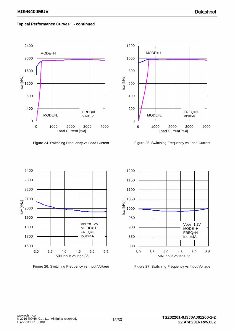
Figure 26. Switching Frequency vs Input Voltage
Figure 27. Switching Frequency vs Input Voltage
Figure 24. Switching Frequency vs Load Current
Figure 25. Switching Frequency vs Load Current
MODE=L
MODE=H
FREQ=H VIN=5V MODE=L
MODE=H
FREQ=L VIN=5V
VOUT=1.2V MODE=H FREQ=L IOUT=4A
VOUT=1.2V MODE=H FREQ=H IOUT=4A

13/30 © 2016 ROHM Co., Ltd. All rights reserved. www.rohm.com
TSZ22111 • 15 • 001
BD9B400MUV
TSZ02201-0J3J0AJ01200-1-2
22.Apr.2016 Rev.002
Typical Performance Curves - continued
Figure 30. Power Up Waveform with VIN (FREQ=H, RLOAD=0.3Ω)
Figure 31. Power Down Waveform with VIN (FREQ=H, RLOAD=0.3Ω)
Figure 28. Power Up Waveform with EN (FREQ=H, RLOAD=0.3Ω)
Figure 29. Power Down Waveform with EN (FREQ=H, RLOAD=0.3Ω)
Time=1ms/div
VIN=5V/div
EN=5V/div
VOUT=1V/div
SW=5V/div
VIN=5V/div
EN=5V/div
VOUT=1V/div
SW=5V/div
Time=1ms/div
VIN=5V/div
EN=5V/div
VOUT=1V/div
SW=5V/div
VIN=5V/div
EN=5V/div
VOUT=1V/div
SW=5V/div
Time=1ms/div Time=1ms/div

14/30 © 2016 ROHM Co., Ltd. All rights reserved. www.rohm.com
TSZ22111 • 15 • 001
BD9B400MUV
TSZ02201-0J3J0AJ01200-1-2
22.Apr.2016 Rev.002
Typical Performance Curves - continued
Figure 35. Switching Waveform (VIN=5V, VOUT=1.2V, FREQ=H, IOUT=4A)
Figure 32. Switching Waveform (VIN=5V, VOUT=1.2V, FREQ=L, IOUT=0.1A)
Figure 33. Switching Waveform (VIN=5V, VOUT=1.2V, FREQ=L, IOUT=4A)
Figure 34. Switching Waveform (VIN=5V, VOUT=1.2V, FREQ=H, IOUT=0.2A)
Time=1µs/div
VOUT=20mV/div
SW=2V/div
VOUT=20mV/div
SW=2V/div
Time=1µs/div
Time=1µs/div
VOUT=20mV/div
SW=2V/div
VOUT=20mV/div
SW=2V/div
Time=1µs/div
15/30 © 2016 ROHM Co., Ltd. All rights reserved. www.rohm.com
TSZ22111 • 15 • 001
BD9B400MUV
TSZ02201-0J3J0AJ01200-1-2
22.Apr.2016 Rev.002
Typical Performance Curves - continued
-3.0
-2.0
-1.0
0.0
1.0
2.0
3.0
0.0 1.0 2.0 3.0 4.0
Load Current [A]
Ou
tpu
t V
olta
ge
De
via
tio
n[%
]-3.0
-2.0
-1.0
0.0
1.0
2.0
3.0
2.5 3.0 3.5 4.0 4.5 5.0 5.5
VIN Input Voltage[V]
Ou
tpu
t V
olta
ge
De
via
tio
n[%
]
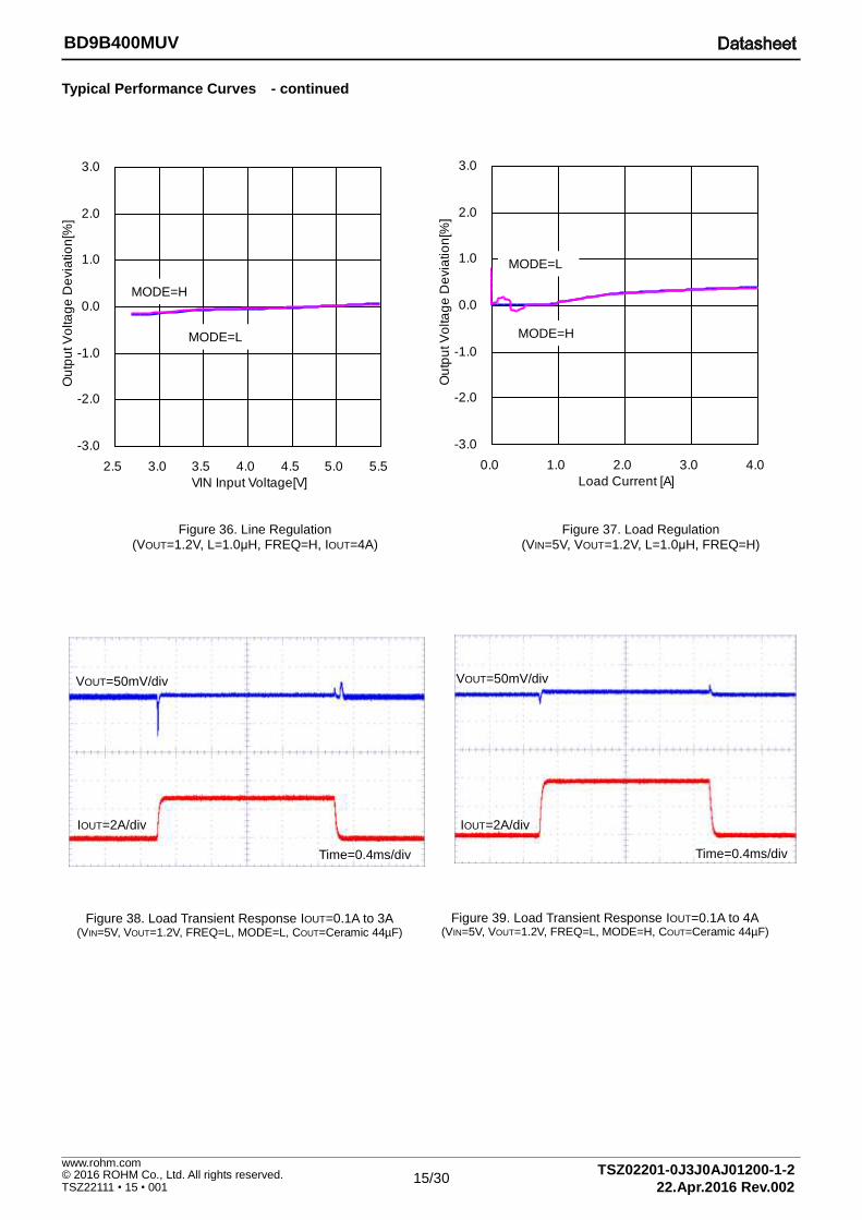
Figure 36. Line Regulation (VOUT=1.2V, L=1.0μH, FREQ=H, IOUT=4A)
Figure 37. Load Regulation (VIN=5V, VOUT=1.2V, L=1.0μH, FREQ=H)
Figure 38. Load Transient Response IOUT=0.1A to 3A (VIN=5V, VOUT=1.2V, FREQ=L, MODE=L, COUT=Ceramic 44µF)
Figure 39. Load Transient Response IOUT=0.1A to 4A (VIN=5V, VOUT=1.2V, FREQ=L, MODE=H, COUT=Ceramic 44µF)
MODE=H
MODE=L
MODE=L
MODE=H
VOUT=50mV/div VOUT=50mV/div
IOUT=2A/div IOUT=2A/div
Time=0.4ms/div Time=0.4ms/div

16/30 © 2016 ROHM Co., Ltd. All rights reserved. www.rohm.com
TSZ22111 • 15 • 001
BD9B400MUV
TSZ02201-0J3J0AJ01200-1-2
22.Apr.2016 Rev.002
Function explanation(s)
1. Basic Operation (1) DC/DC Converter operation
BD9B400MUV is a synchronous rectifying step-down switching regulator that achieves faster transient response by employing constant on-time control system. It utilizes switching operation in PWM (Pulse Width Modulation) mode for heavier load, while it utilizes Deep-SLLM (Deep_Simple Light Load Mode) control for lighter load to improve efficiency.
Figure 40. Efficiency (Deep-SLLM Control and PWM Control)
① Deep-SLLM Control
②PWM Control
VOUT 20mV/div
SW 2.0V/div
VOUT 20mV/div
SW 2.0V/div
② PWM Control
Effic
iency η
[%]
Output Current IOUT [A]
① Deep-SLLM Control
Figure 41. Switching Waveform at Deep-SLLM Control (VIN=5.0V, VOUT=1.2V, IOUT=100mA)
Figure 42. Switching Waveform at PWM Control (VIN=5.0V, VOUT=1.2V, IOUT=4A)

17/30 © 2016 ROHM Co., Ltd. All rights reserved. www.rohm.com
TSZ22111 • 15 • 001
BD9B400MUV
TSZ02201-0J3J0AJ01200-1-2
22.Apr.2016 Rev.002
(2) Enable Control
The IC shutdown can be controlled by the voltage applied to the EN terminal. When VEN reaches 2.0 V(Typ), the internal circuit is activated and the IC starts up. To enable shutdown control with the EN terminal, the shutdown interval (Low level interval of EN) must be set to 100 µs or longer. Startup by EN must be at the same time or after the input of power supply voltage.
Figure 43. Start Up and Down with Enable
(3) Power Good
When the output voltage reaches more than 80% of the voltage setting, the open drain NMOSFET, internally connected to the PGD terminal, turns off and the PGD terminal turns to Hi-z condition. Also when the output voltage falls below 70% of voltage setting, the open drain NMOS FET turns on and PGD terminal pulls down with 100Ω. Connecting a pull up resistor (10KΩ to 100KΩ) is recommended.
Figure 44. Power Good Timing Chart
(4) Soft Start
When EN terminal is turned High, Soft Start operates and output voltage gradually rises. With the Soft Start Function, over shoot of output voltage and rush current can be prevented. Rising time of output voltage when SS terminal is open is 1msec (Typ). Capacitor connected to SS terminal makes rising time more than 1msec. Please refer to page 23 for the method of setting rising time.
Figure 45. Soft Start Timing Chart
VEN
0
VOUT
0Soft start 1 msec
(typ.)
VENH
VENL
EN terminal
Output setting voltage
t
t
EN
VOUT
PGD
Voltage Setting×80%Voltage Setting×70%
EN
VOUT
FB0.8V×90%
1m sec(typ.)※When SS terminal is Open
0.8V

18/30 © 2016 ROHM Co., Ltd. All rights reserved. www.rohm.com
TSZ22111 • 15 • 001
BD9B400MUV
TSZ02201-0J3J0AJ01200-1-2
22.Apr.2016 Rev.002
2. Protection The protective circuits are intended for prevention of damage caused by unexpected accidents. Do not use them for continuous protective operation (1) Over Current Protection (OCP) / Short Circuit Protection (SCP)
Setting (Typ) of over current protection are 7A (lower MOSFET) and 9.5A (upper MOSFET). When OCP is triggered, over current protection is realized by restricting On / Off Duty of current flowing in upper and lower MOSFET by each switching cycle. Also, if Over current protection operates 512 cycles in a condition where FB terminal voltage reaches below 70% of internal standard voltage, Short Circuit protection (SCP) operates and stops switching for 1msec (Typ) before it initiates restart. However, during startup, Short circuit protection will not operate even if the IC is still in the SCP condition.
Table 1. Over Current Protection / Short Circuit Protection Function
EN terminal PGD Startup Over current
protection Short circuit protection
More than 2.0V L
While start up Valid Invalid
Startup completed Valid Valid
H * Valid Invalid
Less than 0.8V * * Invalid Invalid
Figure 46. Short Circuit Protection (SCP) Timing Chart
VOUT
FB
High side OCP threshold
Inside IC OCP signal(Low side)
Inside IC OCP signal(High side)
PGD 512 Cycle
Low side OCP threshold
Coil current
Low sideMOSFET gate
High sideMOSFET gate
1ms(Typ)

19/30 © 2016 ROHM Co., Ltd. All rights reserved. www.rohm.com
TSZ22111 • 15 • 001
BD9B400MUV
TSZ02201-0J3J0AJ01200-1-2
22.Apr.2016 Rev.002
(2) Under Voltage Lockout Protection (UVLO)
The Under Voltage Lockout Protection circuit monitors the AVIN terminal voltage. The operation enters standby when the AVIN terminal voltage is 2.45V (Typ) or lower. The operation starts when the AVIN terminal voltage is 2.55V (Typ) or higher.
Figure 47. UVLO Timing Chart
(3) Thermal Shutdown
When the chip temperature exceeds Tj=175C (Typ), the DC/DC converter output is stopped. The circuits are
automatically restored to normal operation when the chip temperature falls. It has a hysteresis of 25C (Typ). The thermal shutdown circuit is intended for shutting down the IC from thermal runaway in an abnormal state with the
temperature exceeding Tjmax=150C. It is not meant to protect or guarantee the soundness of the application. Do not use the function of this circuit for application protection design.
VIN
0V
VOUT
High side
MOSFET gate
FB
terminal
Soft start
hys
UVLO OFF
UVLO ON
Normal operation Normal operationUVLO
Low side
MOSFET gate

20/30 © 2016 ROHM Co., Ltd. All rights reserved. www.rohm.com
TSZ22111 • 15 • 001
BD9B400MUV
TSZ02201-0J3J0AJ01200-1-2
22.Apr.2016 Rev.002
Application Example(s)
EN
PVIN
BOOT
FREQ
BD9B400MUV
PGD
SW
FB
VOUT
AVIN
SS
PGD
PGND
MODE
C2
C8
L1C10
AGND
R7
R8
C14
VIN
C9
C4
R5
Figure 48. Application Circuit
Table 2. Recommended Component Values (VIN=5V, FREQ=H)
Reference Designator
VOUT Description
1.0V 1.2V 1.5V 1.8V 3.3V
R5 100kΩ 100kΩ 100kΩ 100kΩ 100kΩ -
R7 51kΩ 75kΩ 160kΩ 150kΩ 75kΩ -
R8 200kΩ 150kΩ 180kΩ 120kΩ 24kΩ -
C2(Note 7) 22μF 22μF 22μF 22μF 22μF 10V, X5R, 3216
C4 0.1μF 0.1μF 0.1μF 0.1μF 0.1μF 25V, X5R, 1608
C8(Note 8) 0.1μF 0.1μF 0.1μF 0.1μF 0.1μF -
C9 22μF 22μF 22μF 22μF 22μF 6.3V, X5R, 3225
C10 22μF 22μF 22μF 22μF 22μF 6.3V, X5R, 3225
C14 120pF 120pF 150pF 150pF 180pF -
L1 1.0μH 1.0μH 1.0μH 1.0μH 1.0μH TOKO, FDSD0630
Table 3. Recommended Component Values (VIN=5V, FREQ=L)
Reference Designator
VOUT Description
1.0V 1.2V 1.5V 1.8V 3.3V
R5 100kΩ 100kΩ 100kΩ 100kΩ 100kΩ -
R7 51kΩ 75kΩ 160kΩ 150kΩ 75kΩ -
R8 200kΩ 150kΩ 180kΩ 120kΩ 24kΩ -
C2(Note 7) 22μF 22μF 22μF 22μF 22μF 10V, X5R, 3216
C4 0.1μF 0.1μF 0.1μF 0.1μF 0.1μF 25V, X5R, 1608
C8(Note 8) 0.1μF 0.1μF 0.1μF 0.1μF 0.1μF -
C9 22μF 22μF 22μF 22μF 22μF 6.3V, X5R, 3225
C10 22μF 22μF 22μF 22μF 22μF 6.3V, X5R, 3225
C14 100pF 100pF 120pF 120pF 120pF -
L1 1.0μH 1.0μH 1.0μH 1.0μH 1.0μH TOKO, FDSD0630
(Note 7) For capacitance of input capacitor take temperature characteristics, DC bias characteristics, etc. into consideration to set minimum value to no less than 10μF. (Note 8) For capacitance of bootstrap capacitor take temperature characteristics, DC bias characteristics, etc. into consideration to set minimum value to no less than 0.047μF.
※Evaluation using the actual machine must be done for above constant is only a value on our evaluation board.

21/30 © 2016 ROHM Co., Ltd. All rights reserved. www.rohm.com
TSZ22111 • 15 • 001
BD9B400MUV
TSZ02201-0J3J0AJ01200-1-2
22.Apr.2016 Rev.002
Selection of Components Externally Connected
1. Output LC Filter Constant
In order to supply a continuous current to the load, the DC/DC converter requires an LC filter for smoothing the output voltage. It is recommended to use inductors of values 0.47µH to 1.0µH when FREQ=L or 1.0µH to 1.5µH at FREQ=H.
Figure 49. Waveform of current through inductor Figure 50. Output LC filter circuit
Inductor ripple current ΔIL
Where: VIN= 5V VOUT= 1.2V L=1.0µH fSW=1MHz (switching frequency)
The saturation current of the inductor must be larger than the sum of the maximum output current and 1/2 of the inductor ripple current ∆IL. The output capacitor COUT affects the output ripple voltage characteristics. The output capacitor COUT must satisfy the required ripple voltage characteristics. The output ripple voltage can be represented by the following equation. where RESR is the Equivalent Series Resistance (ESR) of the output capacitor. * The capacitor rating must allow a sufficient margin with respect to the output voltage. The output ripple voltage can be decreased with a smaller ESR. A ceramic capacitor of about 22 µF to 47 µF is recommended.
*Be careful of total capacitance value, when additional capacitor CLOAD is connected in addition to output capacitor COUT.
Use maximum additional capacitor CLOAD (Max) condition which satisfies the following condition.
Maximum starting inductor ripple bottom current ILSTART can be expressed using the following equation.
VOUTL
COUT
PVIN
Driver
mA 912=L×f×V
1×)V(V×V=Δ
SWIN
OUTINOUT -LI
A(min)limitCurrentOver FET side Low<
ILcurrentrippleinductorstartingMaximum START
5.4
bottom
2
ΔI )Icapacitor(outputtocurrentCharge+current(IoutputstartingMaximum=IL L
CAP)OMAXSTART -
V)f×C×8
1+(R×ΔI=ΔV
SWOUT
ESRLRPL
IL
Average inductor current
t
IOUTMAX
Inductor saturation current > IOUTMAX + ΔIL / 2
ΔIL

22/30 © 2016 ROHM Co., Ltd. All rights reserved. www.rohm.com
TSZ22111 • 15 • 001
BD9B400MUV
TSZ02201-0J3J0AJ01200-1-2
22.Apr.2016 Rev.002
Charge current to output capacitor ICAP can be expressed using the following equation.
For example, given VIN= 5V, VOUT= 3.3V, L= 1.5µH, switching frequency fSW= 1.2MHz(Max), Output capacitor COUT= 44µF, Soft Start time TSS= 0.5ms(Min), and load current during soft start IOSS= 4A, maximum CLOAD can be computed using the following equation.
If the value of CLOAD is large, and cannot meet the above equation, adjust the value of the capacitor CSS to meet the
condition below.
(Refer to the following items (3) Soft Start Setting equation of time TSS and soft-start value of the capacitor to be
connected to the CSS.)
For example, given VIN = 5V, VOUT = 3.3V, L = 1.5µH, load current during soft start IOSS = 4A, switching frequency fSW =
1.2MHz (Max), Output capacitor COUT = 44µF, VFB = 0.792V(Max), ISS = 3.6µA(Max), with CLOAD = 220uF, capacitor CSS
is computed as follows.
※CLOAD has an effect on the stability of the DC/DC converter.
To ensure the stability of the DC/DC converter, make sure that a sufficient phase margin is provided.
2. Output Voltage Setting
The output voltage value can be set by the feedback resistance ratio. For stable operation, it is recommended to use feedback resistance R1 of more than 20kΩ.
Figure 51. Feedback Resistor Circuit
VOUT
R1
R2
FB
Error Amplifier
0.8V
V0.8×R2
R2+R1=VOUT
[ ]ASS
OUTLOADOUTCAP T
V×)C+(C=I
μF 78.9C-V
T × /2)ΔII-(4.5< (max)C OUT
OUT
SSLOSSLOAD
Ω
OUT
R1×0.8-V
0.8=R2
OUTSS
SSOUT
FBLOSSLOAD C-C×
I×V
V×/2)ΔII-(4.5<(max)C
pF 2710=)C+(C×V×/2)ΔII-(4.5
I×V>C OUTLOAD
FBLOSS
SSOUTSS

23/30 © 2016 ROHM Co., Ltd. All rights reserved. www.rohm.com
TSZ22111 • 15 • 001
BD9B400MUV
TSZ02201-0J3J0AJ01200-1-2
22.Apr.2016 Rev.002
3. Soft Start Setting
Turning the EN terminal signal High activates the soft start function. This causes the output voltage to rise gradually while the current at startup is placed under control. This allows the prevention of output voltage overshoot and inrush current. The rise time depends on the value of the capacitor connected to the SS terminal.
Turning the EN terminal signal High with the SS terminal open or with the terminal signal High (no capacitor connected) causes the output voltage to rise in 1msec (Typ).
4. FB Capacitor
Generally, in fixed ON time control (hysteresis control), sufficient ripple voltage in FB voltage is needed to operate comparator stably. Regarding this IC, by injecting ripple voltage to FB voltage inside IC it is designed to correspond to low ESR output capacitor. Please set the FB capacitor within the range of the following expression to inject an appropriate ripple.
[msec]
] μF [ [V]] μF [
] μF [with
CurrentSource TerminalStartSoft
(Typ))(0.8VVoltage TerminalFB
TerminalTimeStartSofttoconnectedCapacitor
TimeStartSoft
8.0=
/1.0 0.8× (0.01=T
0.01=C
I
V
C
T
)/VT×(I=C
)/IV×(C=T
SS
SS
SS
FB
SS
SS
FBSSSSSS
SSFBSSSS
)
,
:
:
:
:
))(1.0μA(Typ
Frequency Switching
VoltageOutput
VoltageInput
:
:
:
SW
OUT
IN
SW
IN
OUTOUT
FB
SW
IN
OUTOUT
f
V
V
10 ×3.3×f
)V
V-(1×V
<C< 10 ×7.65×f
)V
V-(1×V
33

24/30 © 2016 ROHM Co., Ltd. All rights reserved. www.rohm.com
TSZ22111 • 15 • 001
BD9B400MUV
TSZ02201-0J3J0AJ01200-1-2
22.Apr.2016 Rev.002
PCB Layout Design
In the step-down DC/DC converter, a large pulse current flows into two loops. The first loop is the one into which the current flows when the High-Side FET is turned ON. The flow starts from the input capacitor CIN, runs through the FET, inductor L and output capacitor COUT and back to GND of CIN via GND of COUT. The second loop is the one into which the current flows when the Low-Side FET is turned on. The flow starts from the Low-Side FET, runs through the inductor L and output capacitor COUT and back to GND of the Low-Side FET via GND of COUT. Route these two loops as thick and as short as possible to allow noise to be reduced for improved efficiency. It is recommended to connect the input and output capacitors directly to the GND plane. The PCB layout has a great influence on the DC/DC converter in terms of all of the heat generation, noise and efficiency characteristics.
Accordingly, design the PCB layout considering the following points.
Connect an input capacitor as close as possible to the IC PVIN terminal on the same plane as the IC.
If there is any unused area on the PCB, provide a copper foil plane for the GND node to assist heat dissipation from
the IC and the surrounding components.
Switching nodes such as SW are susceptible to noise due to AC coupling with other nodes. Route the coil pattern as
thick and as short as possible.
Provide lines connected to FB far from the SW nodes.
Place the output capacitor away from the input capacitor in order to avoid the effect of harmonic noise from the input.
Figure 52. Current Loop of Buck Converter
CIN
MOS FETCOUT
VOUTLVIN

25/30 © 2016 ROHM Co., Ltd. All rights reserved. www.rohm.com
TSZ22111 • 15 • 001
BD9B400MUV
TSZ02201-0J3J0AJ01200-1-2
22.Apr.2016 Rev.002
I/O equivalence circuit(s)
6. FB 7. FREQ
8. MODE 9. SS
10.11.12. SW 13. BOOT
14. PGD 15. EN
SS
AVIN
10kΩ
10kΩ
10kΩ
SW
PVINBOOT
BOOT
PVIN
SW
PGD
AVIN
FB
AVIN
10kΩ
FREQ
AVIN AVIN
100kΩ
EN
390kΩ
470kΩ
140kΩ
MODE
AVIN AVIN
100kΩ
1000kΩ

26/30 © 2016 ROHM Co., Ltd. All rights reserved. www.rohm.com
TSZ22111 • 15 • 001
BD9B400MUV
TSZ02201-0J3J0AJ01200-1-2
22.Apr.2016 Rev.002
Operational Notes
1. Reverse Connection of Power Supply
Connecting the power supply in reverse polarity can damage the IC. Take precautions against reverse polarity when connecting the power supply, such as mounting an external diode between the power supply and the IC’s power supply pins.
2. Power Supply Lines
Design the PCB layout pattern to provide low impedance supply lines. Separate the ground and supply lines of the digital and analog blocks to prevent noise in the ground and supply lines of the digital block from affecting the analog block. Furthermore, connect a capacitor to ground at all power supply pins. Consider the effect of temperature and aging on the capacitance value when using electrolytic capacitors.
3. Ground Voltage
Ensure that no pins are at a voltage below that of the ground pin at any time, even during transient condition. However, pins that drive inductive loads (e.g. motor driver outputs, DC-DC converter outputs) may inevitably go below ground due to back EMF or electromotive force. In such cases, the user should make sure that such voltages going below ground will not cause the IC and the system to malfunction by examining carefully all relevant factors and conditions such as motor characteristics, supply voltage, operating frequency and PCB wiring to name a few.
4. Ground Wiring Pattern
When using both small-signal and large-current ground traces, the two ground traces should be routed separately but connected to a single ground at the reference point of the application board to avoid fluctuations in the small-signal ground caused by large currents. Also ensure that the ground traces of external components do not cause variations on the ground voltage. The ground lines must be as short and thick as possible to reduce line impedance.
5. Thermal Consideration
Should by any chance the maximum junction temperature rating be exceeded the rise in temperature of the chip may result in deterioration of the properties of the chip. In case of exceeding this absolute maximum rating, increase the board size and copper area to prevent exceeding the maximum junction temperature rating.
6. Recommended Operating Conditions
These conditions represent a range within which the expected characteristics of the IC can be approximately obtained. The electrical characteristics are guaranteed under the conditions of each parameter.
7. Inrush Current
When power is first supplied to the IC, it is possible that the internal logic may be unstable and inrush current may flow instantaneously due to the internal powering sequence and delays, especially if the IC has more than one power supply. Therefore, give special consideration to power coupling capacitance, power wiring, width of ground wiring, and routing of connections.
8. Operation Under Strong Electromagnetic Field
Operating the IC in the presence of a strong electromagnetic field may cause the IC to malfunction.
9. Testing on Application Boards
When testing the IC on an application board, connecting a capacitor directly to a low-impedance output pin may subject the IC to stress. Always discharge capacitors completely after each process or step. The IC’s power supply should always be turned off completely before connecting or removing it from the test setup during the inspection process. To prevent damage from static discharge, ground the IC during assembly and use similar precautions during transport and storage.
10. Inter-pin Short and Mounting Errors
Ensure that the direction and position are correct when mounting the IC on the PCB. Incorrect mounting may result in damaging the IC. Avoid nearby pins being shorted to each other especially to ground, power supply and output pin. Inter-pin shorts could be due to many reasons such as metal particles, water droplets (in very humid environment) and unintentional solder bridge deposited in between pins during assembly to name a few.

27/30 © 2016 ROHM Co., Ltd. All rights reserved. www.rohm.com
TSZ22111 • 15 • 001
BD9B400MUV
TSZ02201-0J3J0AJ01200-1-2
22.Apr.2016 Rev.002
Operational Notes – continued
11. Unused Input Pins
Input pins of an IC are often connected to the gate of a MOS transistor. The gate has extremely high impedance and extremely low capacitance. If left unconnected, the electric field from the outside can easily charge it. The small charge acquired in this way is enough to produce a significant effect on the conduction through the transistor and cause unexpected operation of the IC. So unless otherwise specified, unused input pins should be connected to the power supply or ground line.
12. Regarding the Input Pin of the IC
This monolithic IC contains P+ isolation and P substrate layers between adjacent elements in order to keep them isolated. P-N junctions are formed at the intersection of the P layers with the N layers of other elements, creating a parasitic diode or transistor. For example (refer to figure below):
When GND > Pin A and GND > Pin B, the P-N junction operates as a parasitic diode. When GND > Pin B, the P-N junction operates as a parasitic transistor.
Parasitic diodes inevitably occur in the structure of the IC. The operation of parasitic diodes can result in mutual interference among circuits, operational faults, or physical damage. Therefore, conditions that cause these diodes to operate, such as applying a voltage lower than the GND voltage to an input pin (and thus to the P substrate) should be avoided.
Figure 53. Example of monolithic IC structure
13. Ceramic Capacitor
When using a ceramic capacitor, determine the dielectric constant considering the change of capacitance with temperature and the decrease in nominal capacitance due to DC bias and others.
14. Area of Safe Operation (ASO)
Operate the IC such that the output voltage, output current, and power dissipation are all within the Area of Safe Operation (ASO).
15. Thermal Shutdown Circuit(TSD)
This IC has a built-in thermal shutdown circuit that prevents heat damage to the IC. Normal operation should always be within the IC’s power dissipation rating. If however the rating is exceeded for a continued period, the junction temperature (Tj) will rise which will activate the TSD circuit that will turn OFF all output pins. When the Tj falls below the TSD threshold, the circuits are automatically restored to normal operation. Note that the TSD circuit operates in a situation that exceeds the absolute maximum ratings and therefore, under no circumstances, should the TSD circuit be used in a set design or for any purpose other than protecting the IC from heat damage.
16. Over Current Protection Circuit (OCP)
This IC incorporates an integrated overcurrent protection circuit that is activated when the load is shorted. This protection circuit is effective in preventing damage due to sudden and unexpected incidents. However, the IC should not be used in applications characterized by continuous operation or transitioning of the protection circuit.
N NP
+ P
N NP
+
P Substrate
GND
NP
+
N NP
+N P
P Substrate
GND GND
Parasitic
Elements
Pin A
Pin A
Pin B Pin B
B C
E
Parasitic
Elements
GNDParasitic
Elements
CB
E
Transistor (NPN)Resistor
N Region
close-by
Parasitic
Elements

28/30 © 2016 ROHM Co., Ltd. All rights reserved. www.rohm.com
TSZ22111 • 15 • 001
BD9B400MUV
TSZ02201-0J3J0AJ01200-1-2
22.Apr.2016 Rev.002
Ordering Information
B D 9 B 4 0 0 M U V - E 2
Part Number
Package VQFN016V3030
Packaging and forming specification E2: Embossed tape and reel
Marking Diagrams
VQFN016V3030 (TOP VIEW)
D 9 B
4 0 0
Part Number Marking
LOT Number
1PIN MARK

29/30 © 2016 ROHM Co., Ltd. All rights reserved. www.rohm.com
TSZ22111 • 15 • 001
BD9B400MUV
TSZ02201-0J3J0AJ01200-1-2
22.Apr.2016 Rev.002
Physical Dimension, Tape and Reel Information
Package Name VQFN016V3030

30/30 © 2016 ROHM Co., Ltd. All rights reserved. www.rohm.com
TSZ22111 • 15 • 001
BD9B400MUV
TSZ02201-0J3J0AJ01200-1-2
22.Apr.2016 Rev.002
Revision History
Date Revision Changes
1.Mar.2016 001 New Release
22.Apr.2016 002 Page.5 Thermal Resistance - Footprints and Traces
74.2mm2 (Square) ⇒ 74.2mm x 74.2mm

Notice-PGA-E Rev.003
© 2015 ROHM Co., Ltd. All rights reserved.
Notice
Precaution on using ROHM Products 1. Our Products are designed and manufactured for application in ordinary electronic equipments (such as AV equipment,
OA equipment, telecommunication equipment, home electronic appliances, amusement equipment, etc.). If you intend to use our Products in devices requiring extremely high reliability (such as medical equipment
(Note 1), transport
equipment, traffic equipment, aircraft/spacecraft, nuclear power controllers, fuel controllers, car equipment including car accessories, safety devices, etc.) and whose malfunction or failure may cause loss of human life, bodily injury or serious damage to property (“Specific Applications”), please consult with the ROHM sales representative in advance. Unless otherwise agreed in writing by ROHM in advance, ROHM shall not be in any way responsible or liable for any damages, expenses or losses incurred by you or third parties arising from the use of any ROHM’s Products for Specific Applications.
(Note1) Medical Equipment Classification of the Specific Applications
JAPAN USA EU CHINA
CLASSⅢ CLASSⅢ
CLASSⅡb CLASSⅢ
CLASSⅣ CLASSⅢ
2. ROHM designs and manufactures its Products subject to strict quality control system. However, semiconductor
products can fail or malfunction at a certain rate. Please be sure to implement, at your own responsibilities, adequate safety measures including but not limited to fail-safe design against the physical injury, damage to any property, which a failure or malfunction of our Products may cause. The following are examples of safety measures:
[a] Installation of protection circuits or other protective devices to improve system safety [b] Installation of redundant circuits to reduce the impact of single or multiple circuit failure
3. Our Products are designed and manufactured for use under standard conditions and not under any special or extraordinary environments or conditions, as exemplified below. Accordingly, ROHM shall not be in any way responsible or liable for any damages, expenses or losses arising from the use of any ROHM’s Products under any special or extraordinary environments or conditions. If you intend to use our Products under any special or extraordinary environments or conditions (as exemplified below), your independent verification and confirmation of product performance, reliability, etc, prior to use, must be necessary:
[a] Use of our Products in any types of liquid, including water, oils, chemicals, and organic solvents [b] Use of our Products outdoors or in places where the Products are exposed to direct sunlight or dust [c] Use of our Products in places where the Products are exposed to sea wind or corrosive gases, including Cl2,
H2S, NH3, SO2, and NO2
[d] Use of our Products in places where the Products are exposed to static electricity or electromagnetic waves [e] Use of our Products in proximity to heat-producing components, plastic cords, or other flammable items [f] Sealing or coating our Products with resin or other coating materials [g] Use of our Products without cleaning residue of flux (even if you use no-clean type fluxes, cleaning residue of
flux is recommended); or Washing our Products by using water or water-soluble cleaning agents for cleaning residue after soldering
[h] Use of the Products in places subject to dew condensation
4. The Products are not subject to radiation-proof design. 5. Please verify and confirm characteristics of the final or mounted products in using the Products. 6. In particular, if a transient load (a large amount of load applied in a short period of time, such as pulse. is applied,
confirmation of performance characteristics after on-board mounting is strongly recommended. Avoid applying power exceeding normal rated power; exceeding the power rating under steady-state loading condition may negatively affect product performance and reliability.
7. De-rate Power Dissipation depending on ambient temperature. When used in sealed area, confirm that it is the use in
the range that does not exceed the maximum junction temperature. 8. Confirm that operation temperature is within the specified range described in the product specification. 9. ROHM shall not be in any way responsible or liable for failure induced under deviant condition from what is defined in
this document.
Precaution for Mounting / Circuit board design 1. When a highly active halogenous (chlorine, bromine, etc.) flux is used, the residue of flux may negatively affect product
performance and reliability.
2. In principle, the reflow soldering method must be used on a surface-mount products, the flow soldering method must be used on a through hole mount products. If the flow soldering method is preferred on a surface-mount products, please consult with the ROHM representative in advance.
For details, please refer to ROHM Mounting specification

Notice-PGA-E Rev.003
© 2015 ROHM Co., Ltd. All rights reserved.
Precautions Regarding Application Examples and External Circuits 1. If change is made to the constant of an external circuit, please allow a sufficient margin considering variations of the
characteristics of the Products and external components, including transient characteristics, as well as static characteristics.
2. You agree that application notes, reference designs, and associated data and information contained in this document
are presented only as guidance for Products use. Therefore, in case you use such information, you are solely responsible for it and you must exercise your own independent verification and judgment in the use of such information contained in this document. ROHM shall not be in any way responsible or liable for any damages, expenses or losses incurred by you or third parties arising from the use of such information.
Precaution for Electrostatic This Product is electrostatic sensitive product, which may be damaged due to electrostatic discharge. Please take proper caution in your manufacturing process and storage so that voltage exceeding the Products maximum rating will not be applied to Products. Please take special care under dry condition (e.g. Grounding of human body / equipment / solder iron, isolation from charged objects, setting of Ionizer, friction prevention and temperature / humidity control).
Precaution for Storage / Transportation 1. Product performance and soldered connections may deteriorate if the Products are stored in the places where:
[a] the Products are exposed to sea winds or corrosive gases, including Cl2, H2S, NH3, SO2, and NO2 [b] the temperature or humidity exceeds those recommended by ROHM [c] the Products are exposed to direct sunshine or condensation [d] the Products are exposed to high Electrostatic
2. Even under ROHM recommended storage condition, solderability of products out of recommended storage time period may be degraded. It is strongly recommended to confirm solderability before using Products of which storage time is exceeding the recommended storage time period.
3. Store / transport cartons in the correct direction, which is indicated on a carton with a symbol. Otherwise bent leads
may occur due to excessive stress applied when dropping of a carton. 4. Use Products within the specified time after opening a humidity barrier bag. Baking is required before using Products of
which storage time is exceeding the recommended storage time period.
Precaution for Product Label A two-dimensional barcode printed on ROHM Products label is for ROHM’s internal use only.
Precaution for Disposition When disposing Products please dispose them properly using an authorized industry waste company.
Precaution for Foreign Exchange and Foreign Trade act Since concerned goods might be fallen under listed items of export control prescribed by Foreign exchange and Foreign trade act, please consult with ROHM in case of export.
Precaution Regarding Intellectual Property Rights 1. All information and data including but not limited to application example contained in this document is for reference
only. ROHM does not warrant that foregoing information or data will not infringe any intellectual property rights or any other rights of any third party regarding such information or data.
2. ROHM shall not have any obligations where the claims, actions or demands arising from the combination of the Products with other articles such as components, circuits, systems or external equipment (including software).
3. No license, expressly or implied, is granted hereby under any intellectual property rights or other rights of ROHM or any third parties with respect to the Products or the information contained in this document. Provided, however, that ROHM will not assert its intellectual property rights or other rights against you or your customers to the extent necessary to manufacture or sell products containing the Products, subject to the terms and conditions herein.
Other Precaution 1. This document may not be reprinted or reproduced, in whole or in part, without prior written consent of ROHM.
2. The Products may not be disassembled, converted, modified, reproduced or otherwise changed without prior written consent of ROHM.
3. In no event shall you use in any way whatsoever the Products and the related technical information contained in the Products or this document for any military purposes, including but not limited to, the development of mass-destruction weapons.
4. The proper names of companies or products described in this document are trademarks or registered trademarks of ROHM, its affiliated companies or third parties.

DatasheetDatasheet
Notice – WE Rev.001© 2015 ROHM Co., Ltd. All rights reserved.
General Precaution 1. Before you use our Pro ducts, you are requested to care fully read this document and fully understand its contents.
ROHM shall n ot be in an y way responsible or liabl e for fa ilure, malfunction or acci dent arising from the use of a ny ROHM’s Products against warning, caution or note contained in this document.
2. All information contained in this docume nt is current as of the issuing date and subj ect to change without any prior
notice. Before purchasing or using ROHM’s Products, please confirm the la test information with a ROHM sale s representative.
3. The information contained in this doc ument is provi ded on an “as is” basis and ROHM does not warrant that all
information contained in this document is accurate an d/or error-free. ROHM shall not be in an y way responsible or liable for any damages, expenses or losses incurred by you or third parties resulting from inaccuracy or errors of or concerning such information.

Mouser Electronics
Authorized Distributor
Click to View Pricing, Inventory, Delivery & Lifecycle Information: ROHM Semiconductor:
BD9B400MUV-E2
Recommended