DS311 (v23) November 19 2008 wwwxilinxcom 1Product Specification
copy 2004ndash2008 Xilinx Inc All Xilinx trademarks registered trademarks patents and disclaimers are as listed at httpwwwxilinxcomlegalhtm All other trademarks and registered trademarks are the property of their respective owners All specifications are subject to change without notice
Featuresbull Optimized for 18V systems
- As fast as 46 ns pin-to-pin logic delays - As low as 15 μA quiescent current
bull Industryrsquos best 018 micron CMOS CPLD - Optimized architecture for effective logic synthesis- Multi-voltage IO operation mdash 15V to 33V
bull Available in multiple package options- 44-pin VQFP with 33 user IOs- 48-land QFN with 37 user IOs- 56-ball CP BGA with 45 user IOs- 100-pin VQFP with 64 user IOs- Pb-free available for all packages
bull Advanced system features- Fastest in system programming
middot 18V ISP using IEEE 1532 (JTAG) interface- IEEE11491 JTAG Boundary Scan Test- Optional Schmitt-trigger input (per pin)- Two separate IO banks- RealDigital 100 CMOS product term generation- Flexible clocking modes
middot Optional DualEDGE triggered registers- Global signal options with macrocell control
middot Multiple global clocks with phase selection per macrocell
middot Multiple global output enablesmiddot Global setreset
- Efficient control term clocks output enables and setresets for each macrocell and shared across function blocks
- Advanced design security- Optional bus-hold 3-state or weak pullup on
selected IO pins- Open-drain output option for Wired-OR and LED
drive- Optional configurable grounds on unused IOs- Mixed IO voltages compatible with 15V 18V
25V and 33V logic levels- PLA architecture
middot Superior pinout retentionmiddot 100 product term routability across function
block- Hot pluggable
Refer to the CoolRunnertrade-II family data sheet for architec-ture description
DescriptionThe CoolRunner-II 64-macrocell device is designed for bothhigh performance and low power applications This lendspower savings to high-end communication equipment andhigh speed to battery operated devices Due to the lowpower stand-by and dynamic operation overall system reli-ability is improved
This device consists of four Function Blocks inter-connectedby a low power Advanced Interconnect Matrix (AIM) TheAIM feeds 40 true and complement inputs to each FunctionBlock The Function Blocks consist of a 40 by 56 P-termPLA and 16 macrocells which contain numerous configura-tion bits that allow for combinational or registered modes ofoperation
Additionally these registers can be globally reset or presetand configured as a D or T flip-flop or as a D latch Thereare also multiple clock signals both global and local productterm types configured on a per macrocell basis Output pinconfigurations include slew rate limit bus hold pull-upopen drain and programmable grounds A Schmitt triggerinput is available on a per input pin basis In addition to stor-ing macrocell output states the macrocell registers can beconfigured as direct input registers to store signals directlyfrom input pins
Clocking is available on a global or Function Block basisThree global clocks are available for all Function Blocks as asynchronous clock source Macrocell registers can be indi-vidually configured to power up to the zero or one state Aglobal setreset control line is also available to asynchro-nously set or reset selected registers during operationAdditional local clock synchronous clock-enable asynchro-nous setreset and output enable signals can be formedusing product terms on a per-macrocell or per-FunctionBlock basis
A DualEDGE flip-flop feature is also available on a per mac-rocell basis This feature allows high performance synchro-nous operation based on lower frequency clocking to helpreduce the total power consumption of the device
The CoolRunner-II 64-macrocell CPLD is IO compatiblewith standard LVTTL and LVCMOS18 LVCMOS25 andLVCMOS33 (see Table 1) This device is also 15V IO com-patible with the use of Schmitt-trigger inputs
Another feature that eases voltage translation is IO bank-ing Two IO banks are available on the CoolRunner-II 64Amacrocell device that permit easy interfacing to 33V 25V18V and 15V devices
0
XC2C64A CoolRunner-II CPLD
DS311 (v23) November 19 2008 0 0 Product Specification
R
XC2C64A CoolRunner-II CPLD
2 wwwxilinxcom DS311 (v23) November 19 2008Product Specification
R
RealDigital Design TechnologyXilinxreg CoolRunner-II CPLDs are fabricated on a018 micron process technology which is derived from lead-ing edge FPGA product development CoolRunner-IICPLDs employ RealDigital a design technique that makesuse of CMOS technology in both the fabrication and designmethodology RealDigital design technology employs a cas-cade of CMOS gates to implement sum of products insteadof traditional sense amplifier methodology Due to this tech-nology Xilinx CoolRunner-II CPLDs achieve both high per-formance and low power operation
Supported IO StandardsThe CoolRunner-II 64 macrocell features both LVCMOSand LVTTL IO implementations See Table 1 for IO stan-dard voltages The LVTTL IO standard is a general purposeEIAJEDEC standard for 33V applications that use an
LVTTL input buffer and Push-Pull output buffer TheLVCMOS standard is used in 33V 25V and 18V applica-tions CoolRunner-II CPLDs are also 15V IO compatiblewith the use of Schmitt-trigger inputs
Table 1 IO Standards for XC2C64A
IOSTANDARD Attribute
Output VCCIO
Input VCCIO
Input VREF
Board TerminationVoltage VT
LVTTL 33 33 NA NA
LVCMOS33 33 33 NA NA
LVCMOS25 25 25 NA NA
LVCMOS18 18 18 NA NA
LVCMOS15(1) 15 15 NA NA
1 LVCMOS15 requires Schmitt-trigger inputs
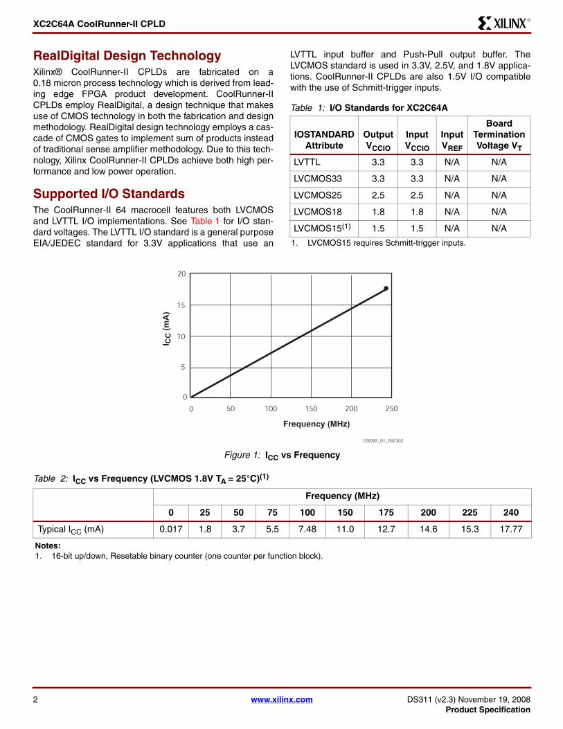
Figure 1 ICC vs Frequency
Table 2 ICC vs Frequency (LVCMOS 18V TA = 25degC)(1)
Frequency (MHz)
0 25 50 75 100 150 175 200 225 240
Typical ICC (mA) 0017 18 37 55 748 110 127 146 153 1777
Notes 1 16-bit updown Resetable binary counter (one counter per function block)
Frequency (MHz)
DS092_01_092302
I CC
(m
A)
0
0
10
5
15
20
25020015010050
XC2C64A CoolRunner-II CPLD
DS311 (v23) November 19 2008 wwwxilinxcom 3Product Specification
R
Recommended Operating Conditions
DC Electrical Characteristics Over Recommended Operating Conditions
Absolute Maximum RatingsSymbol Description Value Units
VCC Supply voltage relative to ground ndash05 to 20 V
VCCIO Supply voltage for output drivers ndash05 to 40 V
VJTAG(2) JTAG input voltage limits ndash05 to 40 V
VCCAUX JTAG input supply voltage ndash05 to 40 V
VIN(1) Input voltage relative to ground(1) ndash05 to 40 V
VTS(1) Voltage applied to 3-state output(1) ndash05 to 40 V
VSTG(3) Storage Temperature (ambient) ndash65 to +150 degC
TJ Junction Temperature +150 degC
Notes 1 Maximum DC undershoot below GND must be limited to either 05V or 10 mA whichever is easiest to achieve During transitions
the device pins might undershoot to ndash20V or overshoot to +45V provided this overshoot or undershoot lasts less than 10 ns and with the forcing current being limited to 200 mA
2 Valid over commercial temperature range3 For soldering guidelines and thermal considerations see the Device Packaging information on the Xilinx website For Pb free
packages see XAPP427
Symbol Parameter Min Max Units
VCC Supply voltage for internal logic and input buffers
Commercial TA = 0degC to +70degC 17 19 V
Industrial TA = ndash40degC to +85degC 17 19 V
VCCIO Supply voltage for output drivers 33V operation 30 36 V
Supply voltage for output drivers 25V operation 23 27 V
Supply voltage for output drivers 18V operation 17 19 V
Supply voltage for output drivers 15V operation 14 16 V
VCCAUX JTAG programming pins 17 36 V
Symbol Parameter Test Conditions Typical Max Units
ICCSB Standby current Commercial VCC = 19V VCCIO = 36V 31 100 μA
ICCSB Standby current Industrial VCC = 19V VCCIO = 36V 43 165 μA
ICC(1) Dynamic current f = 1 MHz - 500 μA
f = 50 MHz - 5 mA
CJTAG JTAG input capacitance f = 1 MHz - 10 pF
CCLK Global clock input capacitance f = 1 MHz - 12 pF
CIO IO capacitance f = 1 MHz - 10 pF
IIL(2) Input leakage current VIN = 0V or VCCIO to 39V - +ndash1 μA
IIH(2) IO High-Z leakage VIN = 0V or VCCIO to 39V - +ndash1 μA
Notes 1 16-bit updown Resetable binary counter (one counter per function block) tested at VCC=VCCIO= 19V2 See Quality and Reliability section of the CoolRunner-II family data sheet
XC2C64A CoolRunner-II CPLD
4 wwwxilinxcom DS311 (v23) November 19 2008Product Specification
R
LVCMOS 33V and LVTTL 33V DC Voltage Specifications
LVCMOS 25V DC Voltage Specifications
LVCMOS 18V DC Voltage Specifications
Symbol Parameter Test Conditions Min Max Units
VCCIO Input source voltage 30 36 V
VIH High level input voltage 2 39 V
VIL Low level input voltage ndash03 08 V
VOH High level output voltage IOH = ndash8 mA VCCIO = 3V VCCIO ndash 04V - V
IOH = ndash01 mA VCCIO = 3V VCCIO ndash 02V - V
VOL Low level output voltage IOL = 8 mA VCCIO = 3V - 04 V
IOL = 01 mA VCCIO = 3V - 02 V
Symbol Parameter Test Conditions Min Max Units
VCCIO Input source voltage 23 27 V
VIH High level input voltage 17 VCCIO + 03(1) V
VIL Low level input voltage ndash03 07 V
VOH High level output voltage IOH = ndash8 mA VCCIO = 23V VCCIO ndash 04V - V
IOH = ndash01 mA VCCIO = 23V VCCIO ndash 02V - V
VOL Low level output voltage IOL = 8 mA VCCIO = 23V - 04 V
IOL = 01 mA VCCIO = 23V - 02 V
1 The VIH Max value represents the JEDEC specification for LVCMOS25 The CoolRunner-II CPLD input buffer can tolerate up to 39V without physical damage
Symbol Parameter Test Conditions Min Max Units
VCCIO Input source voltage - 17 19 V
VIH High level input voltage - 065 x VCCIO VCCIO + 03(1) V
VIL Low level input voltage - ndash03 035 x VCCIO V
VOH High level output voltage IOH = ndash8 mA VCCIO = 17V VCCIO ndash 045 - V
IOH = ndash01 mA VCCIO = 17V VCCIO ndash 02 - V
VOL Low level output voltage IOL = 8 mA VCCIO = 17V - 045 V
IOL = 01 mA VCCIO = 17V - 02 V
1 The VIH Max value represents the JEDEC specification for LVCMOS18 The CoolRunner-II CPLD input buffer can tolerate up to 39V without physical damage
XC2C64A CoolRunner-II CPLD
DS311 (v23) November 19 2008 wwwxilinxcom 5Product Specification
R
LVCMOS 15V DC Voltage Specifications
Schmitt Trigger Input DC Voltage Specifications
Symbol Parameter(1) Test Conditions Min Max Units
VCCIO Input source voltage - 14 16 V
VT+ Input hysteresis threshold voltage - 05 x VCCIO 08 x VCCIO V
VT- - 02 x VCCIO 05 x VCCIO V
VOH High level output voltage IOH = ndash8 mA VCCIO = 14V VCCIO ndash 045 - V
IOH = ndash01 mA VCCIO = 14V VCCIO ndash 02 - V
VOL Low level output voltage IOL = 8 mA VCCIO = 14V - 04 V
IOL = 01 mA VCCIO = 14V - 02 V
Notes 1 Hysteresis used on 15V inputs
Symbol Parameter Test Conditions Min Max Units
VCCIO Input source voltage - 14 39 V
VT+ Input hysteresis threshold voltage - 05 x VCCIO 08 x VCCIO V
VT- - 02 x VCCIO 05 x VCCIO V
XC2C64A CoolRunner-II CPLD
6 wwwxilinxcom DS311 (v23) November 19 2008Product Specification
R
AC Electrical Characteristics Over Recommended Operating Conditions
Symbol Parameter
-5 -7
UnitsMin Max Min Max
TPD1 Propagation delay single p-term - 46 - 67 ns
TPD2 Propagation delay OR array - 50 - 75 ns
TSUD Direct input register clock setup time 24 - 33 - ns
TSU1 Setup time (single p-term) 20 - 25 - ns
TSU2 Setup time (OR array) 24 - 33 - ns
THD Direct input register hold time 0 - 0 - ns
TH P-term hold time 0 - 0 - ns
TCO Clock to output - 39 - 60 ns
FTOGGLE(1) Internal toggle rate(1) - 500 - 300 MHz
FSYSTEM1(2) Maximum system frequency(2) - 263 - 159 MHz
FSYSTEM2(2) Maximum system frequency(2) - 238 - 141 MHz
FEXT1(3) Maximum external frequency(3) - 169 - 118 MHz
FEXT2(3) Maximum external frequency(3) - 159 - 108 MHz
TPSUD Direct input register p-term clock setup time 09 - 17 - ns
TPSU1 P-term clock setup time (single p-term) 06 - 09 - ns
TPSU2 P-term clock setup time (OR array) 10 - 17 - ns
TPHD Direct input register p-term clock hold time 13 - 14 - ns
TPH P-term clock hold 15 - 17 - ns
TPCO P-term clock to output - 60 - 84 ns
TOETOD Global OE to output enabledisable - 80 - 100 ns
TPOETPOD P-term OE to output enabledisable - 90 - 110 ns
TMOETMOD Macrocell driven OE to output enabledisable - 90 - 110 ns
TPAO P-term setreset to output valid - 73 - 97 ns
TAO Global setreset to output valid - 60 - 83 ns
TSUEC Register clock enable setup time 30 - 37 - ns
THEC Register clock enable hold time 0 - 0 - ns
TCW Global clock pulse width High or Low 14 - 22 - ns
TPCW P-term pulse width High or Low 50 - 75 - ns
TAPRPW Asynchronous presetreset pulse width (High or Low) 50 - 75 - ns
TCONFIG(4) Configuration time - 500 - 500 μs
Notes 1 FTOGGLE is the maximum frequency of a dual edge triggered T flip-flop with output enabled2 FSYSTEM (1TCYCLE) is the internal operating frequency for a device fully populated with 16-bit updown Resetable binary counter
(one counter per function block)3 FEXT (1TSU1+TCO) is the maximum external frequency4 Typical configuration current during TCONFIG is 23 mA
XC2C64A CoolRunner-II CPLD
DS311 (v23) November 19 2008 wwwxilinxcom 7Product Specification
R
Internal Timing Parameters
Symbol Parameter(1)
-5 -7
UnitsMin Max Min Max
Buffer Delays
TIN Input buffer delay - 17 - 24 ns
TDIN Direct data register input delay - 26 - 40 ns
TGCK Global clock buffer delay - 16 - 25 ns
TGSR Global setreset buffer delay - 24 - 35 ns
TGTS Global 3-state buffer delay - 27 - 39 ns
TOUT Output buffer delay - 19 - 28 ns
TEN Output buffer enabledisable delay - 53 - 61 ns
P-term Delays
TCT Control term delay - 20 - 25 ns
TLOGI1 Single P-term delay adder - 05 - 08 ns
TLOGI2 Multiple P-term delay adder - 04 - 08 ns
Macrocell Delay
TPDI Input to output valid - 05 - 07 ns
TSUI Setup before clock 14 - 18 - ns
THI Hold after clock 00 - 00 - ns
TECSU Enable clock setup time 09 - 13 - ns
TECHO Enable clock hold time 0 - 0 - ns
TCOI Clock to output valid - 04 - 07 ns
TAOI Setreset to output valid - 17 - 20 ns
TCDBL Clock doubler delay - 0 - 0 ns
Feedback Delays
TF Feedback delay - 15 - 30 ns
TOEM Macrocell to global OE delay - 17 - 17 ns
IO Standard Time Adder Delays 15V CMOS
THYS15 Hysteresis input adder - 40 - 60 ns
TOUT15 Output adder - 09 - 15 ns
TSLEW15 Output slew rate adder - 40 - 60 ns
IO Standard Time Adder Delays 18V CMOS
THYS18 Hysteresis input adder - 30 - 40 ns
TOUT18 Output adder - 0 - 0 ns
TSLEW Output slew rate adder - 35 - 50 ns
XC2C64A CoolRunner-II CPLD
8 wwwxilinxcom DS311 (v23) November 19 2008Product Specification
R
IO Standard Time Adder Delays 25V CMOS
TIN25 Standard input adder - 05 - 06 ns
THYS25 Hysteresis input adder - 25 - 30 ns
TOUT25 Output adder - 08 - 09 ns
TSLEW25 Output slew rate adder - 40 - 50 ns
IO Standard Time Adder Delays 33V CMOSTTL
TIN33 Standard input adder - 05 - 06 ns
THYS33 Hysteresis input adder - 20 - 30 ns
TOUT33 Output adder - 12 - 14 ns
TSLEW33 Output slew rate adder - 40 - 50 ns
1 15 ns input pin signal risefall
Internal Timing Parameters (Continued)
Symbol Parameter(1)
-5 -7
UnitsMin Max Min Max
XC2C64A CoolRunner-II CPLD
DS311 (v23) November 19 2008 wwwxilinxcom 9Product Specification
R
Switching Characteristics
AC Test Circuit
Typical IO Output Curves
Figure 4 Typical IO Output Curves
Figure 2 Derating Curve for TPD
Figure 3 AC Load Circuit
Number of Outputs Switching
1 2 4 8 1630
40
50
VCC = VCCIO = 18V T = 25oC
T PD2
(ns)
55
45
35
DS092_02_092302
R1
VCC
CLR2
Device Under Test
Output Type
LVTTL33
LVCMOS33
LVCMOS25
LVCMOS18
LVCMOS15
R1268Ω 275Ω188Ω
1125Ω150Ω
R2235Ω275Ω188Ω
1125Ω150Ω
CL35 pF
35 pF
35 pF
35 pF
35 pF
DS311_03_102108
Test Point
Notes1 CL includes test fixtures and probe capacitance 2 15 ns maximum risefall times on inputs
Vo Output Volts
IO O
utpu
t Cur
rent
(mA
)
Vdde1
15V
18V25V
33V
XC2C64A CoolRunner-II CPLD
10 wwwxilinxcom DS311 (v23) November 19 2008Product Specification
R
Pin DescriptionsFunction Block Macrocell PC44(1) VQ44 QFG48 CP56 VQ100 IO Banking
1 1 44 38 F1 13 Bank 2
1 2 43 37 5 E3 12 Bank 2
1 3 42 36 4 E1 11 Bank 2
1 4 - - - 10 Bank 2
1 5 - - - 9 Bank 2
1 6 - - - 8 Bank 2
1 7 - - - 7 Bank 2
1 8 - - - 6 Bank 2
1(GTS1) 9 40 34 2 D1 4 Bank 2
1(GTS0) 10 39 33 1 C1 3 Bank 2
1(GTS3) 11 38 32 48 A3 2 Bank 2
1(GTS2) 12 37 31 47 A2 1 Bank 2
1(GSR) 13 36 30 46 B1 99 Bank 2
1 14 - - A1 97 Bank 2
1 15 - - C3 94 Bank 2
1 16 - - - 92 Bank 2
2 1 1 39 6 G1 14 Bank 1
2 2 2 40 7 F3 15 Bank 1
2 3 - - 8 - 16 Bank 1
2 4 - - 9 - 17 Bank 1
2 5 3 41 10 H1 18 Bank 1
2 6 4 42 G3 19 Bank 1
2(GCK0) 7 5 43 11 J1 22 Bank 1
2(GCK1) 8 6 44 12 K1 23 Bank 1
2 9 - - K4 24 Bank 1
2(GCK2) 10 7 1 13 K2 27 Bank 1
2 11 - - - 28 Bank 1
2 12 8 2 14 K3 29 Bank 1
2 13 9 3 15 H3 30 Bank 1
2 14 - - K5 32 Bank 1
2 15 - - - 33 Bank 1
2 16 - - - 34 Bank 1
XC2C64A CoolRunner-II CPLD
DS311 (v23) November 19 2008 wwwxilinxcom 11Product Specification
R
3 1 35 29 45 C4 91 Bank 2
3 2 34 28 44 A4 90 Bank 2
3 3 33 27 43 C5 89 Bank 2
3 4 - - A7 81 Bank 2
3 5 - - 39 C8 79 Bank 2
3 6 29 23 38 A8 78 Bank 2
3 7 - - A9 77 Bank 2
3 8 - - - 76 Bank 2
3 9 - - 37 A5 74 Bank 2
3 10 28 22 36 A10 72 Bank 2
3 11 27 21 35 B10 71 Bank 2
3 12 26 20 34 C10 70 Bank 2
3 13 - - D8 68 Bank 2
3 14 25 19 33 E8 67 Bank 2
3 15 24 18 32 D10 64 Bank 2
3 16 - - - 61 Bank 2
4 1 11 5 17 K6 35 Bank 1
4 2 12 6 18 H5 36 Bank 1
4 3 - - K7 37 Bank 1
4 4 - - - 39 Bank 1
4 5 - - H7 40 Bank 1
4 6 - - - 41 Bank 1
4 7 14 8 20 H8 42 Bank 1
4 8 - - - 43 Bank 1
4 9 - - - 49 Bank 1
4 10 - - 24 K8 50 Bank 1
4 11 18 12 25 H10 52 Bank 1
4 12 - - 26 - 53 Bank 1
4 13 19 13 27 G10 55 Bank 1
4 14 20 14 28 - 56 Bank 1
4 15 22 16 F10 58 Bank 1
4 16 - - 30 E10 60 Bank 1
1 This is an obsolete package type It remains here for legacy support only2 GTS = global output enable GSR = global set reset GCK = global clock3 GCK GSR and GTS pins can also be used for general purpose IOs
Pin Descriptions (Continued)Function Block Macrocell PC44(1) VQ44 QFG48 CP56 VQ100 IO Banking
XC2C64A CoolRunner-II CPLD
12 wwwxilinxcom DS311 (v23) November 19 2008Product Specification
R
XC2C64A Global JTAG PowerGround and No Connect Pins
Ordering Information
Pin Type PC44(1) VQ44 QFG48 CP56 VQ100
TCK 17 11 23 K10 48
TDI 15 9 21 J10 45
TDO 30 24 40 A6 83
TMS 16 10 22 K9 47
VCCAUX (JTAG supply voltage) 41 35 3 D3 5
Power internal (VCC)
Power bank 1 IO (VCCIO1)
Power bank 2 IO (VCCIO2)
21 15 29 G8 2657
13 7 19 H6 38 51
32 26 42 C6 88 98
Ground 10 23 31 41725 16 31 41 H4 F8 C7 21 31 62 69 84100
No connects 20 25 44 46 54 59 63 65 66 73 75 80 82 85 86 87 93 95
96
Total user IO 33 33 37 45 641 This is an obsolete package type It remains here for legacy support only
Device Ordering Noand Part Marking No
PinBallSpacing
θJA(degCWatt)
θJC(CWatt) Package Type
Package BodyDimensions IO
Comm(C)Ind (I)(1)
XC2C64A-5QFG48C 05mm 312 212 Quad Flat No Lead 7mm x 7mm 37 C
XC2C64A-7QFG48C 05mm 312 212 Quad Flat No Lead 7mm x 7mm 37 C
XC2C64A-5VQ44C 08mm 466 82 Very Thin Quad Flat Pack 10mm x 10mm 33 C
XC2C64A-7VQ44C 08mm 466 82 Very Thin Quad Flat Pack 10mm x 10mm 33 C
XC2C64A-5CP56C 05mm 650 150 Chip Scale Package 6mm x 6mm 45 C
XC2C64A-7CP56C 05mm 650 150 Chip Scale Package 6mm x 6mm 45 C
XC2C64A-5VQ100C 05mm 532 146 Very Thin Quad Flat Pack 14mm x 14mm 64 C
XC2C64A-7VQ100C 05mm 532 146 Very Thin Quad Flat Pack 14mm x 14mm 64 C
XC2C64A-5VQG44C 08mm 466 82 Very Thin Quad Flat Pack Pb-free
10mm x 10mm 33 C
XC2C64A-7VQG44C 08mm 466 82 Very Thin Quad Flat Pack Pb-free
10mm x 10mm 33 C
XC2C64A-5CPG56C 05mm 650 150 Chip Scale Package Pb-free
6mm x 6mm 45 C
XC2C64A-7CPG56C 05mm 650 150 Chip Scale Package Pb-free
6mm x 6mm 45 C
XC2C64A-5VQG100C 05mm 532 146 Very Thin Quad Flat Pack Pb-free
14mm x 14mm 64 C
XC2C64A-7VQG100C 05mm 532 146 Very Thin Quad Flat Pack Pb-free
14mm x 14mm 64 C
XC2C64A-7VQ44I 08mm 466 82 Very Thin Quad Flat Pack 10mm x 10mm 33 I
XC2C64A-7QFG48I 05mm 312 212 Quad Flat No Lead Pb-free
7mm x 7mm 37 I
XC2C64A-7CP56I 05mm 650 150 Chip Scale Package 6mm x 6mm 45 I
XC2C64A-7VQ100I 05mm 532 146 Very Thin Quad Flat Pack 14mm x 14mm 64 I
XC2C64A CoolRunner-II CPLD
DS311 (v23) November 19 2008 wwwxilinxcom 13Product Specification
R
Device Part Marking
Figure 5 Sample Package with Part Marking
Note Due to the small size of chip scale and quad flat no lead packages the complete ordering part number cannot beincluded on the package marking Part marking on chip scale and quad flat no lead packages by line are
1 X (Xilinx logo) then truncated part number
2 Not related to device part number
3 Not related to device part number
4 Device code speed operating temperature three digits not related to device part number Device codes C3 = CP56 C4 = CPG56 Q2 = QFG48
XC2C64A-7VQG44I 08mm 466 82 Very Thin Quad Flat Pack Pb-free
10mm x 10mm 33 I
XC2C64A-7CPG56I 05mm 650 150 Chip Scale Package Pb-free
6mm x 6mm 45 I
XC2C64A-7VQG100I 05mm 532 146 Very Thin Quad Flat Pack Pb-free
14mm x 14mm 64 I
Notes 1 C = Commercial (TA = 0degC to +70degC) I = Industrial (TA = ndash40degC to +85degC)
Device Ordering Noand Part Marking No
PinBallSpacing
θJA(degCWatt)
θJC(CWatt) Package Type
Package BodyDimensions IO
Comm(C)Ind (I)(1)
Standard Example XC2C128 Device Speed Grade Package Type Number of Pins Temperature Range
-4 TQ C144 Pb-Free Example XC2C128 TQ G 144 C
Device Speed Grade Package Type Pb-FreeNumber of Pins
-4
Temperature Range
XC2CxxxTQ144
7C
Device Type
Package
Speed
Operating Range
This line notrelated to devicepart number
R
Part marking for non-chip scale packageDS311_05_102108
XC2C64A CoolRunner-II CPLD
14 wwwxilinxcom DS311 (v23) November 19 2008Product Specification
R
Package Pinout Diagrams
Figure 6 VQ44 Package
Figure 7 PC44 Package (Obsolete package shown for legacy support only)
VQ44Top View
IO(1)
IO(1)
IO(1)
IO(3)
IOIOIOVCCIO2GNDTDOIO
IO(2
)
IO(2
)
IO IO IO IO IO IO IO VA
UX
IO(1
)
IO IO IO VC
CIO
GN
DIO IO IO IO IO
IO(2)
IOIO
GNDIOIO
VCCIO1IOTDI
TMSTCK
1234567891011
12 13 14 15 16 17 18 19 20 21 22
3332313029282726252423
44 43 42 41 40 39 38 37 36 35 34
(1) - Global Output Enable(2) - Global Clock(3) - Global SetReset
PC44Top View
IO(1)
IO(1)
IO(1)
IO(3)
IOIOIOVCCIO2GndTDOIO
IO(2
)
IO(2
)
IO IO IO IO IO IO IO VA
UX
IO(1
)
IO IO IO VC
CIO
GN
DIO IO IO IO IO
IO(2)
IOIO
GNDIOIO
VCCIO1IOTDI
TMSTCK
7891011121314151617
18 19 20 21 22 23 24 25 26 27 28
3938373635343332313029
6 5 4 3 2 1 44 43 42 41 40
(1) - Global Output Enable(2) - Global Clock(3) - Global SetReset
Figure 8 QFG48 Package
Figure 9 CP56 Package
QFG48Top View
IOIOIOIOIOGndIOVccIOIOIOIO
IO(1
)IO
(1)
IO(3
)IO IO IO Vc
cio2
Gnd
TDO
IO IO IO
IO(2
)IO IO G
ndIO IO Vc
cio1
IO TDI
TMS
TCK
IO
IO(1)IO(1)VAUXIOIOIOIOIOIOIOIO(2)IO(2)
123456789101112 13 14 15 16 17 18 19 20 21 22 23 24
363534333231302928272625
48 47 46 45 44 43 42 41 40 39 38 37
(1) - Global Output Enable
(2) - Global Clock
(3) - Global SetReset
CP56Bottom View
IO(2) IO(2) IO IO IO IO IO IO TMS TCK
IO(2) TDI
IO IO GND IO VCCIO1 IO IO IO
IO IO VCC IO
IO IO GND IO
IO IO IO IO
IO(1) VAUX IO IO
IO(1) IO IO IO VCCIO2 GND IO IO
IO(3) IO
IO IO(1) IO(1) IO IO TDO IO IO IO IO
K
J
H
G
F
E
D
C
B
A
1 2 3 4 5 6 7 8 9 10
(1) - Global Output Enable(2) - Global Clock(3) - Global SetReset
XC2C64A CoolRunner-II CPLD
DS311 (v23) November 19 2008 wwwxilinxcom 15Product Specification
R
Warranty DisclaimerTHESE PRODUCTS ARE SUBJECT TO THE TERMS OF THE XILINX LIMITED WARRANTY WHICH CAN BE VIEWEDAT httpwwwxilinxcomwarrantyhtm THIS LIMITED WARRANTY DOES NOT EXTEND TO ANY USE OF THEPRODUCTS IN AN APPLICATION OR ENVIRONMENT THAT IS NOT WITHIN THE SPECIFICATIONS STATED ON THETHEN-CURRENT XILINX DATA SHEET FOR THE PRODUCTS PRODUCTS ARE NOT DESIGNED TO BE FAIL-SAFEAND ARE NOT WARRANTED FOR USE IN APPLICATIONS THAT POSE A RISK OF PHYSICAL HARM OR LOSS OFLIFE USE OF PRODUCTS IN SUCH APPLICATIONS IS FULLY AT THE RISK OF CUSTOMER SUBJECT TOAPPLICABLE LAWS AND REGULATIONS
Figure 12 VQ100 Package
VQ100Top View
GN
DIO
(3)
VC
CIO
2IO N
CN
CIO N
CIO IO IO IO V
CC
IO2
NC
NC
NC
GN
DT
DO
NC
IO NC
IO IO IO IO
VC
CIO
(2)
IO IO IOG
ND
IO IO IO IO IO IOV
CC
IO1
IO IO IO IO IO NC
TD
IN
CT
MS
TC
KIO IO
NCIONCIOIOIOGNDIOIONCNCIONCGNDIOIONCIOVccIOIONCIOIOVCCIO1
IO(1)
IO(1)
IO(1)
IO(1)
VAUXIOIOIOIOIOIOIOIOIOIOIOIOIOIONC
GNDIO(2)
IO(2)
IONC
12345678910111213141516171819202122232425
75747372717069686766656463626160595857565554535251
26 27 28 29 30 31 32 33 34 35 36 37 38 39 40 41 42 43 44 45 46 47 48 49 50
100 99 98 97 96 95 94 93 92 91 90 89 88 87 86 85 84 83 82 81 80 79 78 77 76
(1) - Global Output Enable(2) - Global Clock(3) - Global SetReset
XC2C64A CoolRunner-II CPLD
16 wwwxilinxcom DS311 (v23) November 19 2008Product Specification
R
Additional InformationAdditional information is available for the followingCoolRunner-II CPLD topics atwwwxilinxcomsupportdocumentationcoolrunner-iihtm
bull Device pinouts in the density specific data sheetsbull Termination power sequencing voltage thresholds
and slew rate data in the CPLD IO User Guide
bull Reliability data in the Device Reliability Reportbull Packaging thermal and electrical data in the Device
Package User Guide
Package drawings and dimensions are available atwwwxilinxcomsupportdocumentationpackage_specificationshtm
Revision HistoryThe following table shows the revision history for this document
Date Version Revision
51504 10 Initial Xilinx release
83004 11 Pb-free documentation
100104 12 Add Asynchronous PresetReset Pulse Width specification to AC Electrical Characteristics
110804 13 Product Release No change to documentation
112904 14 Change to QFG package drawing (Figure 8) Pin 29 relabelled
121404 15 Changes to Figure 4 Typical IO Output Curves Changes to tOUT25 and tOUT33 Internal Timing Parameters page 8
011805 16 Changes to ICCSB fTOGGLE tPSU1 tPSU2 tPHD tCW tSLEW25 and tSLEW33
030705 17 Format change to specifications IIL and IIH page 3 Improvement to pin-to-pin logic delay page 1 Modifications to Table 1 IOSTANDARDs
062805 18 Move to Product Specification Change to TIN25 TOUT25 TIN33 and TOUT33
013006 19 Modified footnote 1 from AC Specifications Table to remove incorrect equation
032006 20 Add Warranty Disclaimer Add note to Pin Descriptions that GCK GSR and GTS pins can also be used for general purpose IO
021507 21 Change to VIH specification for 25V and 18V LVCMOS Change TF specification on -7 speed grade from 20 to 30 ns
030807 22 Fixed typo in note for VIL for LVCMOS18 removed note for VIL for LVCMOS33
111908 23 Added note to Pin Description tables to indicate the PC44 packages are obsolete Removed part numbers for devices in PC44 packages the Features section and from the ordering information See Product Discontinuation Notice xcn07022pdf
XC2C64A CoolRunner-II CPLD
2 wwwxilinxcom DS311 (v23) November 19 2008Product Specification
R
RealDigital Design TechnologyXilinxreg CoolRunner-II CPLDs are fabricated on a018 micron process technology which is derived from lead-ing edge FPGA product development CoolRunner-IICPLDs employ RealDigital a design technique that makesuse of CMOS technology in both the fabrication and designmethodology RealDigital design technology employs a cas-cade of CMOS gates to implement sum of products insteadof traditional sense amplifier methodology Due to this tech-nology Xilinx CoolRunner-II CPLDs achieve both high per-formance and low power operation
Supported IO StandardsThe CoolRunner-II 64 macrocell features both LVCMOSand LVTTL IO implementations See Table 1 for IO stan-dard voltages The LVTTL IO standard is a general purposeEIAJEDEC standard for 33V applications that use an
LVTTL input buffer and Push-Pull output buffer TheLVCMOS standard is used in 33V 25V and 18V applica-tions CoolRunner-II CPLDs are also 15V IO compatiblewith the use of Schmitt-trigger inputs
Table 1 IO Standards for XC2C64A
IOSTANDARD Attribute
Output VCCIO
Input VCCIO
Input VREF
Board TerminationVoltage VT
LVTTL 33 33 NA NA
LVCMOS33 33 33 NA NA
LVCMOS25 25 25 NA NA
LVCMOS18 18 18 NA NA
LVCMOS15(1) 15 15 NA NA
1 LVCMOS15 requires Schmitt-trigger inputs
Figure 1 ICC vs Frequency
Table 2 ICC vs Frequency (LVCMOS 18V TA = 25degC)(1)
Frequency (MHz)
0 25 50 75 100 150 175 200 225 240
Typical ICC (mA) 0017 18 37 55 748 110 127 146 153 1777
Notes 1 16-bit updown Resetable binary counter (one counter per function block)
Frequency (MHz)
DS092_01_092302
I CC
(m
A)
0
0
10
5
15
20
25020015010050
XC2C64A CoolRunner-II CPLD
DS311 (v23) November 19 2008 wwwxilinxcom 3Product Specification
R
Recommended Operating Conditions
DC Electrical Characteristics Over Recommended Operating Conditions
Absolute Maximum RatingsSymbol Description Value Units
VCC Supply voltage relative to ground ndash05 to 20 V
VCCIO Supply voltage for output drivers ndash05 to 40 V
VJTAG(2) JTAG input voltage limits ndash05 to 40 V
VCCAUX JTAG input supply voltage ndash05 to 40 V
VIN(1) Input voltage relative to ground(1) ndash05 to 40 V
VTS(1) Voltage applied to 3-state output(1) ndash05 to 40 V
VSTG(3) Storage Temperature (ambient) ndash65 to +150 degC
TJ Junction Temperature +150 degC
Notes 1 Maximum DC undershoot below GND must be limited to either 05V or 10 mA whichever is easiest to achieve During transitions
the device pins might undershoot to ndash20V or overshoot to +45V provided this overshoot or undershoot lasts less than 10 ns and with the forcing current being limited to 200 mA
2 Valid over commercial temperature range3 For soldering guidelines and thermal considerations see the Device Packaging information on the Xilinx website For Pb free
packages see XAPP427
Symbol Parameter Min Max Units
VCC Supply voltage for internal logic and input buffers
Commercial TA = 0degC to +70degC 17 19 V
Industrial TA = ndash40degC to +85degC 17 19 V
VCCIO Supply voltage for output drivers 33V operation 30 36 V
Supply voltage for output drivers 25V operation 23 27 V
Supply voltage for output drivers 18V operation 17 19 V
Supply voltage for output drivers 15V operation 14 16 V
VCCAUX JTAG programming pins 17 36 V
Symbol Parameter Test Conditions Typical Max Units
ICCSB Standby current Commercial VCC = 19V VCCIO = 36V 31 100 μA
ICCSB Standby current Industrial VCC = 19V VCCIO = 36V 43 165 μA
ICC(1) Dynamic current f = 1 MHz - 500 μA
f = 50 MHz - 5 mA
CJTAG JTAG input capacitance f = 1 MHz - 10 pF
CCLK Global clock input capacitance f = 1 MHz - 12 pF
CIO IO capacitance f = 1 MHz - 10 pF
IIL(2) Input leakage current VIN = 0V or VCCIO to 39V - +ndash1 μA
IIH(2) IO High-Z leakage VIN = 0V or VCCIO to 39V - +ndash1 μA
Notes 1 16-bit updown Resetable binary counter (one counter per function block) tested at VCC=VCCIO= 19V2 See Quality and Reliability section of the CoolRunner-II family data sheet
XC2C64A CoolRunner-II CPLD
4 wwwxilinxcom DS311 (v23) November 19 2008Product Specification
R
LVCMOS 33V and LVTTL 33V DC Voltage Specifications
LVCMOS 25V DC Voltage Specifications
LVCMOS 18V DC Voltage Specifications
Symbol Parameter Test Conditions Min Max Units
VCCIO Input source voltage 30 36 V
VIH High level input voltage 2 39 V
VIL Low level input voltage ndash03 08 V
VOH High level output voltage IOH = ndash8 mA VCCIO = 3V VCCIO ndash 04V - V
IOH = ndash01 mA VCCIO = 3V VCCIO ndash 02V - V
VOL Low level output voltage IOL = 8 mA VCCIO = 3V - 04 V
IOL = 01 mA VCCIO = 3V - 02 V
Symbol Parameter Test Conditions Min Max Units
VCCIO Input source voltage 23 27 V
VIH High level input voltage 17 VCCIO + 03(1) V
VIL Low level input voltage ndash03 07 V
VOH High level output voltage IOH = ndash8 mA VCCIO = 23V VCCIO ndash 04V - V
IOH = ndash01 mA VCCIO = 23V VCCIO ndash 02V - V
VOL Low level output voltage IOL = 8 mA VCCIO = 23V - 04 V
IOL = 01 mA VCCIO = 23V - 02 V
1 The VIH Max value represents the JEDEC specification for LVCMOS25 The CoolRunner-II CPLD input buffer can tolerate up to 39V without physical damage
Symbol Parameter Test Conditions Min Max Units
VCCIO Input source voltage - 17 19 V
VIH High level input voltage - 065 x VCCIO VCCIO + 03(1) V
VIL Low level input voltage - ndash03 035 x VCCIO V
VOH High level output voltage IOH = ndash8 mA VCCIO = 17V VCCIO ndash 045 - V
IOH = ndash01 mA VCCIO = 17V VCCIO ndash 02 - V
VOL Low level output voltage IOL = 8 mA VCCIO = 17V - 045 V
IOL = 01 mA VCCIO = 17V - 02 V
1 The VIH Max value represents the JEDEC specification for LVCMOS18 The CoolRunner-II CPLD input buffer can tolerate up to 39V without physical damage
XC2C64A CoolRunner-II CPLD
DS311 (v23) November 19 2008 wwwxilinxcom 5Product Specification
R
LVCMOS 15V DC Voltage Specifications
Schmitt Trigger Input DC Voltage Specifications
Symbol Parameter(1) Test Conditions Min Max Units
VCCIO Input source voltage - 14 16 V
VT+ Input hysteresis threshold voltage - 05 x VCCIO 08 x VCCIO V
VT- - 02 x VCCIO 05 x VCCIO V
VOH High level output voltage IOH = ndash8 mA VCCIO = 14V VCCIO ndash 045 - V
IOH = ndash01 mA VCCIO = 14V VCCIO ndash 02 - V
VOL Low level output voltage IOL = 8 mA VCCIO = 14V - 04 V
IOL = 01 mA VCCIO = 14V - 02 V
Notes 1 Hysteresis used on 15V inputs
Symbol Parameter Test Conditions Min Max Units
VCCIO Input source voltage - 14 39 V
VT+ Input hysteresis threshold voltage - 05 x VCCIO 08 x VCCIO V
VT- - 02 x VCCIO 05 x VCCIO V
XC2C64A CoolRunner-II CPLD
6 wwwxilinxcom DS311 (v23) November 19 2008Product Specification
R
AC Electrical Characteristics Over Recommended Operating Conditions
Symbol Parameter
-5 -7
UnitsMin Max Min Max
TPD1 Propagation delay single p-term - 46 - 67 ns
TPD2 Propagation delay OR array - 50 - 75 ns
TSUD Direct input register clock setup time 24 - 33 - ns
TSU1 Setup time (single p-term) 20 - 25 - ns
TSU2 Setup time (OR array) 24 - 33 - ns
THD Direct input register hold time 0 - 0 - ns
TH P-term hold time 0 - 0 - ns
TCO Clock to output - 39 - 60 ns
FTOGGLE(1) Internal toggle rate(1) - 500 - 300 MHz
FSYSTEM1(2) Maximum system frequency(2) - 263 - 159 MHz
FSYSTEM2(2) Maximum system frequency(2) - 238 - 141 MHz
FEXT1(3) Maximum external frequency(3) - 169 - 118 MHz
FEXT2(3) Maximum external frequency(3) - 159 - 108 MHz
TPSUD Direct input register p-term clock setup time 09 - 17 - ns
TPSU1 P-term clock setup time (single p-term) 06 - 09 - ns
TPSU2 P-term clock setup time (OR array) 10 - 17 - ns
TPHD Direct input register p-term clock hold time 13 - 14 - ns
TPH P-term clock hold 15 - 17 - ns
TPCO P-term clock to output - 60 - 84 ns
TOETOD Global OE to output enabledisable - 80 - 100 ns
TPOETPOD P-term OE to output enabledisable - 90 - 110 ns
TMOETMOD Macrocell driven OE to output enabledisable - 90 - 110 ns
TPAO P-term setreset to output valid - 73 - 97 ns
TAO Global setreset to output valid - 60 - 83 ns
TSUEC Register clock enable setup time 30 - 37 - ns
THEC Register clock enable hold time 0 - 0 - ns
TCW Global clock pulse width High or Low 14 - 22 - ns
TPCW P-term pulse width High or Low 50 - 75 - ns
TAPRPW Asynchronous presetreset pulse width (High or Low) 50 - 75 - ns
TCONFIG(4) Configuration time - 500 - 500 μs
Notes 1 FTOGGLE is the maximum frequency of a dual edge triggered T flip-flop with output enabled2 FSYSTEM (1TCYCLE) is the internal operating frequency for a device fully populated with 16-bit updown Resetable binary counter
(one counter per function block)3 FEXT (1TSU1+TCO) is the maximum external frequency4 Typical configuration current during TCONFIG is 23 mA
XC2C64A CoolRunner-II CPLD
DS311 (v23) November 19 2008 wwwxilinxcom 7Product Specification
R
Internal Timing Parameters
Symbol Parameter(1)
-5 -7
UnitsMin Max Min Max
Buffer Delays
TIN Input buffer delay - 17 - 24 ns
TDIN Direct data register input delay - 26 - 40 ns
TGCK Global clock buffer delay - 16 - 25 ns
TGSR Global setreset buffer delay - 24 - 35 ns
TGTS Global 3-state buffer delay - 27 - 39 ns
TOUT Output buffer delay - 19 - 28 ns
TEN Output buffer enabledisable delay - 53 - 61 ns
P-term Delays
TCT Control term delay - 20 - 25 ns
TLOGI1 Single P-term delay adder - 05 - 08 ns
TLOGI2 Multiple P-term delay adder - 04 - 08 ns
Macrocell Delay
TPDI Input to output valid - 05 - 07 ns
TSUI Setup before clock 14 - 18 - ns
THI Hold after clock 00 - 00 - ns
TECSU Enable clock setup time 09 - 13 - ns
TECHO Enable clock hold time 0 - 0 - ns
TCOI Clock to output valid - 04 - 07 ns
TAOI Setreset to output valid - 17 - 20 ns
TCDBL Clock doubler delay - 0 - 0 ns
Feedback Delays
TF Feedback delay - 15 - 30 ns
TOEM Macrocell to global OE delay - 17 - 17 ns
IO Standard Time Adder Delays 15V CMOS
THYS15 Hysteresis input adder - 40 - 60 ns
TOUT15 Output adder - 09 - 15 ns
TSLEW15 Output slew rate adder - 40 - 60 ns
IO Standard Time Adder Delays 18V CMOS
THYS18 Hysteresis input adder - 30 - 40 ns
TOUT18 Output adder - 0 - 0 ns
TSLEW Output slew rate adder - 35 - 50 ns
XC2C64A CoolRunner-II CPLD
8 wwwxilinxcom DS311 (v23) November 19 2008Product Specification
R
IO Standard Time Adder Delays 25V CMOS
TIN25 Standard input adder - 05 - 06 ns
THYS25 Hysteresis input adder - 25 - 30 ns
TOUT25 Output adder - 08 - 09 ns
TSLEW25 Output slew rate adder - 40 - 50 ns
IO Standard Time Adder Delays 33V CMOSTTL
TIN33 Standard input adder - 05 - 06 ns
THYS33 Hysteresis input adder - 20 - 30 ns
TOUT33 Output adder - 12 - 14 ns
TSLEW33 Output slew rate adder - 40 - 50 ns
1 15 ns input pin signal risefall
Internal Timing Parameters (Continued)
Symbol Parameter(1)
-5 -7
UnitsMin Max Min Max
XC2C64A CoolRunner-II CPLD
DS311 (v23) November 19 2008 wwwxilinxcom 9Product Specification
R
Switching Characteristics
AC Test Circuit
Typical IO Output Curves
Figure 4 Typical IO Output Curves
Figure 2 Derating Curve for TPD
Figure 3 AC Load Circuit
Number of Outputs Switching
1 2 4 8 1630
40
50
VCC = VCCIO = 18V T = 25oC
T PD2
(ns)
55
45
35
DS092_02_092302
R1
VCC
CLR2
Device Under Test
Output Type
LVTTL33
LVCMOS33
LVCMOS25
LVCMOS18
LVCMOS15
R1268Ω 275Ω188Ω
1125Ω150Ω
R2235Ω275Ω188Ω
1125Ω150Ω
CL35 pF
35 pF
35 pF
35 pF
35 pF
DS311_03_102108
Test Point
Notes1 CL includes test fixtures and probe capacitance 2 15 ns maximum risefall times on inputs
Vo Output Volts
IO O
utpu
t Cur
rent
(mA
)
Vdde1
15V
18V25V
33V
XC2C64A CoolRunner-II CPLD
10 wwwxilinxcom DS311 (v23) November 19 2008Product Specification
R
Pin DescriptionsFunction Block Macrocell PC44(1) VQ44 QFG48 CP56 VQ100 IO Banking
1 1 44 38 F1 13 Bank 2
1 2 43 37 5 E3 12 Bank 2
1 3 42 36 4 E1 11 Bank 2
1 4 - - - 10 Bank 2
1 5 - - - 9 Bank 2
1 6 - - - 8 Bank 2
1 7 - - - 7 Bank 2
1 8 - - - 6 Bank 2
1(GTS1) 9 40 34 2 D1 4 Bank 2
1(GTS0) 10 39 33 1 C1 3 Bank 2
1(GTS3) 11 38 32 48 A3 2 Bank 2
1(GTS2) 12 37 31 47 A2 1 Bank 2
1(GSR) 13 36 30 46 B1 99 Bank 2
1 14 - - A1 97 Bank 2
1 15 - - C3 94 Bank 2
1 16 - - - 92 Bank 2
2 1 1 39 6 G1 14 Bank 1
2 2 2 40 7 F3 15 Bank 1
2 3 - - 8 - 16 Bank 1
2 4 - - 9 - 17 Bank 1
2 5 3 41 10 H1 18 Bank 1
2 6 4 42 G3 19 Bank 1
2(GCK0) 7 5 43 11 J1 22 Bank 1
2(GCK1) 8 6 44 12 K1 23 Bank 1
2 9 - - K4 24 Bank 1
2(GCK2) 10 7 1 13 K2 27 Bank 1
2 11 - - - 28 Bank 1
2 12 8 2 14 K3 29 Bank 1
2 13 9 3 15 H3 30 Bank 1
2 14 - - K5 32 Bank 1
2 15 - - - 33 Bank 1
2 16 - - - 34 Bank 1
XC2C64A CoolRunner-II CPLD
DS311 (v23) November 19 2008 wwwxilinxcom 11Product Specification
R
3 1 35 29 45 C4 91 Bank 2
3 2 34 28 44 A4 90 Bank 2
3 3 33 27 43 C5 89 Bank 2
3 4 - - A7 81 Bank 2
3 5 - - 39 C8 79 Bank 2
3 6 29 23 38 A8 78 Bank 2
3 7 - - A9 77 Bank 2
3 8 - - - 76 Bank 2
3 9 - - 37 A5 74 Bank 2
3 10 28 22 36 A10 72 Bank 2
3 11 27 21 35 B10 71 Bank 2
3 12 26 20 34 C10 70 Bank 2
3 13 - - D8 68 Bank 2
3 14 25 19 33 E8 67 Bank 2
3 15 24 18 32 D10 64 Bank 2
3 16 - - - 61 Bank 2
4 1 11 5 17 K6 35 Bank 1
4 2 12 6 18 H5 36 Bank 1
4 3 - - K7 37 Bank 1
4 4 - - - 39 Bank 1
4 5 - - H7 40 Bank 1
4 6 - - - 41 Bank 1
4 7 14 8 20 H8 42 Bank 1
4 8 - - - 43 Bank 1
4 9 - - - 49 Bank 1
4 10 - - 24 K8 50 Bank 1
4 11 18 12 25 H10 52 Bank 1
4 12 - - 26 - 53 Bank 1
4 13 19 13 27 G10 55 Bank 1
4 14 20 14 28 - 56 Bank 1
4 15 22 16 F10 58 Bank 1
4 16 - - 30 E10 60 Bank 1
1 This is an obsolete package type It remains here for legacy support only2 GTS = global output enable GSR = global set reset GCK = global clock3 GCK GSR and GTS pins can also be used for general purpose IOs
Pin Descriptions (Continued)Function Block Macrocell PC44(1) VQ44 QFG48 CP56 VQ100 IO Banking
XC2C64A CoolRunner-II CPLD
12 wwwxilinxcom DS311 (v23) November 19 2008Product Specification
R
XC2C64A Global JTAG PowerGround and No Connect Pins
Ordering Information
Pin Type PC44(1) VQ44 QFG48 CP56 VQ100
TCK 17 11 23 K10 48
TDI 15 9 21 J10 45
TDO 30 24 40 A6 83
TMS 16 10 22 K9 47
VCCAUX (JTAG supply voltage) 41 35 3 D3 5
Power internal (VCC)
Power bank 1 IO (VCCIO1)
Power bank 2 IO (VCCIO2)
21 15 29 G8 2657
13 7 19 H6 38 51
32 26 42 C6 88 98
Ground 10 23 31 41725 16 31 41 H4 F8 C7 21 31 62 69 84100
No connects 20 25 44 46 54 59 63 65 66 73 75 80 82 85 86 87 93 95
96
Total user IO 33 33 37 45 641 This is an obsolete package type It remains here for legacy support only
Device Ordering Noand Part Marking No
PinBallSpacing
θJA(degCWatt)
θJC(CWatt) Package Type
Package BodyDimensions IO
Comm(C)Ind (I)(1)
XC2C64A-5QFG48C 05mm 312 212 Quad Flat No Lead 7mm x 7mm 37 C
XC2C64A-7QFG48C 05mm 312 212 Quad Flat No Lead 7mm x 7mm 37 C
XC2C64A-5VQ44C 08mm 466 82 Very Thin Quad Flat Pack 10mm x 10mm 33 C
XC2C64A-7VQ44C 08mm 466 82 Very Thin Quad Flat Pack 10mm x 10mm 33 C
XC2C64A-5CP56C 05mm 650 150 Chip Scale Package 6mm x 6mm 45 C
XC2C64A-7CP56C 05mm 650 150 Chip Scale Package 6mm x 6mm 45 C
XC2C64A-5VQ100C 05mm 532 146 Very Thin Quad Flat Pack 14mm x 14mm 64 C
XC2C64A-7VQ100C 05mm 532 146 Very Thin Quad Flat Pack 14mm x 14mm 64 C
XC2C64A-5VQG44C 08mm 466 82 Very Thin Quad Flat Pack Pb-free
10mm x 10mm 33 C
XC2C64A-7VQG44C 08mm 466 82 Very Thin Quad Flat Pack Pb-free
10mm x 10mm 33 C
XC2C64A-5CPG56C 05mm 650 150 Chip Scale Package Pb-free
6mm x 6mm 45 C
XC2C64A-7CPG56C 05mm 650 150 Chip Scale Package Pb-free
6mm x 6mm 45 C
XC2C64A-5VQG100C 05mm 532 146 Very Thin Quad Flat Pack Pb-free
14mm x 14mm 64 C
XC2C64A-7VQG100C 05mm 532 146 Very Thin Quad Flat Pack Pb-free
14mm x 14mm 64 C
XC2C64A-7VQ44I 08mm 466 82 Very Thin Quad Flat Pack 10mm x 10mm 33 I
XC2C64A-7QFG48I 05mm 312 212 Quad Flat No Lead Pb-free
7mm x 7mm 37 I
XC2C64A-7CP56I 05mm 650 150 Chip Scale Package 6mm x 6mm 45 I
XC2C64A-7VQ100I 05mm 532 146 Very Thin Quad Flat Pack 14mm x 14mm 64 I
XC2C64A CoolRunner-II CPLD
DS311 (v23) November 19 2008 wwwxilinxcom 13Product Specification
R
Device Part Marking
Figure 5 Sample Package with Part Marking
Note Due to the small size of chip scale and quad flat no lead packages the complete ordering part number cannot beincluded on the package marking Part marking on chip scale and quad flat no lead packages by line are
1 X (Xilinx logo) then truncated part number
2 Not related to device part number
3 Not related to device part number
4 Device code speed operating temperature three digits not related to device part number Device codes C3 = CP56 C4 = CPG56 Q2 = QFG48
XC2C64A-7VQG44I 08mm 466 82 Very Thin Quad Flat Pack Pb-free
10mm x 10mm 33 I
XC2C64A-7CPG56I 05mm 650 150 Chip Scale Package Pb-free
6mm x 6mm 45 I
XC2C64A-7VQG100I 05mm 532 146 Very Thin Quad Flat Pack Pb-free
14mm x 14mm 64 I
Notes 1 C = Commercial (TA = 0degC to +70degC) I = Industrial (TA = ndash40degC to +85degC)
Device Ordering Noand Part Marking No
PinBallSpacing
θJA(degCWatt)
θJC(CWatt) Package Type
Package BodyDimensions IO
Comm(C)Ind (I)(1)
Standard Example XC2C128 Device Speed Grade Package Type Number of Pins Temperature Range
-4 TQ C144 Pb-Free Example XC2C128 TQ G 144 C
Device Speed Grade Package Type Pb-FreeNumber of Pins
-4
Temperature Range
XC2CxxxTQ144
7C
Device Type
Package
Speed
Operating Range
This line notrelated to devicepart number
R
Part marking for non-chip scale packageDS311_05_102108
XC2C64A CoolRunner-II CPLD
14 wwwxilinxcom DS311 (v23) November 19 2008Product Specification
R
Package Pinout Diagrams
Figure 6 VQ44 Package
Figure 7 PC44 Package (Obsolete package shown for legacy support only)
VQ44Top View
IO(1)
IO(1)
IO(1)
IO(3)
IOIOIOVCCIO2GNDTDOIO
IO(2
)
IO(2
)
IO IO IO IO IO IO IO VA
UX
IO(1
)
IO IO IO VC
CIO
GN
DIO IO IO IO IO
IO(2)
IOIO
GNDIOIO
VCCIO1IOTDI
TMSTCK
1234567891011
12 13 14 15 16 17 18 19 20 21 22
3332313029282726252423
44 43 42 41 40 39 38 37 36 35 34
(1) - Global Output Enable(2) - Global Clock(3) - Global SetReset
PC44Top View
IO(1)
IO(1)
IO(1)
IO(3)
IOIOIOVCCIO2GndTDOIO
IO(2
)
IO(2
)
IO IO IO IO IO IO IO VA
UX
IO(1
)
IO IO IO VC
CIO
GN
DIO IO IO IO IO
IO(2)
IOIO
GNDIOIO
VCCIO1IOTDI
TMSTCK
7891011121314151617
18 19 20 21 22 23 24 25 26 27 28
3938373635343332313029
6 5 4 3 2 1 44 43 42 41 40
(1) - Global Output Enable(2) - Global Clock(3) - Global SetReset
Figure 8 QFG48 Package
Figure 9 CP56 Package
QFG48Top View
IOIOIOIOIOGndIOVccIOIOIOIO
IO(1
)IO
(1)
IO(3
)IO IO IO Vc
cio2
Gnd
TDO
IO IO IO
IO(2
)IO IO G
ndIO IO Vc
cio1
IO TDI
TMS
TCK
IO
IO(1)IO(1)VAUXIOIOIOIOIOIOIOIO(2)IO(2)
123456789101112 13 14 15 16 17 18 19 20 21 22 23 24
363534333231302928272625
48 47 46 45 44 43 42 41 40 39 38 37
(1) - Global Output Enable
(2) - Global Clock
(3) - Global SetReset
CP56Bottom View
IO(2) IO(2) IO IO IO IO IO IO TMS TCK
IO(2) TDI
IO IO GND IO VCCIO1 IO IO IO
IO IO VCC IO
IO IO GND IO
IO IO IO IO
IO(1) VAUX IO IO
IO(1) IO IO IO VCCIO2 GND IO IO
IO(3) IO
IO IO(1) IO(1) IO IO TDO IO IO IO IO
K
J
H
G
F
E
D
C
B
A
1 2 3 4 5 6 7 8 9 10
(1) - Global Output Enable(2) - Global Clock(3) - Global SetReset
XC2C64A CoolRunner-II CPLD
DS311 (v23) November 19 2008 wwwxilinxcom 15Product Specification
R
Warranty DisclaimerTHESE PRODUCTS ARE SUBJECT TO THE TERMS OF THE XILINX LIMITED WARRANTY WHICH CAN BE VIEWEDAT httpwwwxilinxcomwarrantyhtm THIS LIMITED WARRANTY DOES NOT EXTEND TO ANY USE OF THEPRODUCTS IN AN APPLICATION OR ENVIRONMENT THAT IS NOT WITHIN THE SPECIFICATIONS STATED ON THETHEN-CURRENT XILINX DATA SHEET FOR THE PRODUCTS PRODUCTS ARE NOT DESIGNED TO BE FAIL-SAFEAND ARE NOT WARRANTED FOR USE IN APPLICATIONS THAT POSE A RISK OF PHYSICAL HARM OR LOSS OFLIFE USE OF PRODUCTS IN SUCH APPLICATIONS IS FULLY AT THE RISK OF CUSTOMER SUBJECT TOAPPLICABLE LAWS AND REGULATIONS
Figure 12 VQ100 Package
VQ100Top View
GN
DIO
(3)
VC
CIO
2IO N
CN
CIO N
CIO IO IO IO V
CC
IO2
NC
NC
NC
GN
DT
DO
NC
IO NC
IO IO IO IO
VC
CIO
(2)
IO IO IOG
ND
IO IO IO IO IO IOV
CC
IO1
IO IO IO IO IO NC
TD
IN
CT
MS
TC
KIO IO
NCIONCIOIOIOGNDIOIONCNCIONCGNDIOIONCIOVccIOIONCIOIOVCCIO1
IO(1)
IO(1)
IO(1)
IO(1)
VAUXIOIOIOIOIOIOIOIOIOIOIOIOIOIONC
GNDIO(2)
IO(2)
IONC
12345678910111213141516171819202122232425
75747372717069686766656463626160595857565554535251
26 27 28 29 30 31 32 33 34 35 36 37 38 39 40 41 42 43 44 45 46 47 48 49 50
100 99 98 97 96 95 94 93 92 91 90 89 88 87 86 85 84 83 82 81 80 79 78 77 76
(1) - Global Output Enable(2) - Global Clock(3) - Global SetReset
XC2C64A CoolRunner-II CPLD
16 wwwxilinxcom DS311 (v23) November 19 2008Product Specification
R
Additional InformationAdditional information is available for the followingCoolRunner-II CPLD topics atwwwxilinxcomsupportdocumentationcoolrunner-iihtm
bull Device pinouts in the density specific data sheetsbull Termination power sequencing voltage thresholds
and slew rate data in the CPLD IO User Guide
bull Reliability data in the Device Reliability Reportbull Packaging thermal and electrical data in the Device
Package User Guide
Package drawings and dimensions are available atwwwxilinxcomsupportdocumentationpackage_specificationshtm
Revision HistoryThe following table shows the revision history for this document
Date Version Revision
51504 10 Initial Xilinx release
83004 11 Pb-free documentation
100104 12 Add Asynchronous PresetReset Pulse Width specification to AC Electrical Characteristics
110804 13 Product Release No change to documentation
112904 14 Change to QFG package drawing (Figure 8) Pin 29 relabelled
121404 15 Changes to Figure 4 Typical IO Output Curves Changes to tOUT25 and tOUT33 Internal Timing Parameters page 8
011805 16 Changes to ICCSB fTOGGLE tPSU1 tPSU2 tPHD tCW tSLEW25 and tSLEW33
030705 17 Format change to specifications IIL and IIH page 3 Improvement to pin-to-pin logic delay page 1 Modifications to Table 1 IOSTANDARDs
062805 18 Move to Product Specification Change to TIN25 TOUT25 TIN33 and TOUT33
013006 19 Modified footnote 1 from AC Specifications Table to remove incorrect equation
032006 20 Add Warranty Disclaimer Add note to Pin Descriptions that GCK GSR and GTS pins can also be used for general purpose IO
021507 21 Change to VIH specification for 25V and 18V LVCMOS Change TF specification on -7 speed grade from 20 to 30 ns
030807 22 Fixed typo in note for VIL for LVCMOS18 removed note for VIL for LVCMOS33
111908 23 Added note to Pin Description tables to indicate the PC44 packages are obsolete Removed part numbers for devices in PC44 packages the Features section and from the ordering information See Product Discontinuation Notice xcn07022pdf

XC2C64A CoolRunner-II CPLD
DS311 (v23) November 19 2008 wwwxilinxcom 3Product Specification
R
Recommended Operating Conditions
DC Electrical Characteristics Over Recommended Operating Conditions
Absolute Maximum RatingsSymbol Description Value Units
VCC Supply voltage relative to ground ndash05 to 20 V
VCCIO Supply voltage for output drivers ndash05 to 40 V
VJTAG(2) JTAG input voltage limits ndash05 to 40 V
VCCAUX JTAG input supply voltage ndash05 to 40 V
VIN(1) Input voltage relative to ground(1) ndash05 to 40 V
VTS(1) Voltage applied to 3-state output(1) ndash05 to 40 V
VSTG(3) Storage Temperature (ambient) ndash65 to +150 degC
TJ Junction Temperature +150 degC
Notes 1 Maximum DC undershoot below GND must be limited to either 05V or 10 mA whichever is easiest to achieve During transitions
the device pins might undershoot to ndash20V or overshoot to +45V provided this overshoot or undershoot lasts less than 10 ns and with the forcing current being limited to 200 mA
2 Valid over commercial temperature range3 For soldering guidelines and thermal considerations see the Device Packaging information on the Xilinx website For Pb free
packages see XAPP427
Symbol Parameter Min Max Units
VCC Supply voltage for internal logic and input buffers
Commercial TA = 0degC to +70degC 17 19 V
Industrial TA = ndash40degC to +85degC 17 19 V
VCCIO Supply voltage for output drivers 33V operation 30 36 V
Supply voltage for output drivers 25V operation 23 27 V
Supply voltage for output drivers 18V operation 17 19 V
Supply voltage for output drivers 15V operation 14 16 V
VCCAUX JTAG programming pins 17 36 V
Symbol Parameter Test Conditions Typical Max Units
ICCSB Standby current Commercial VCC = 19V VCCIO = 36V 31 100 μA
ICCSB Standby current Industrial VCC = 19V VCCIO = 36V 43 165 μA
ICC(1) Dynamic current f = 1 MHz - 500 μA
f = 50 MHz - 5 mA
CJTAG JTAG input capacitance f = 1 MHz - 10 pF
CCLK Global clock input capacitance f = 1 MHz - 12 pF
CIO IO capacitance f = 1 MHz - 10 pF
IIL(2) Input leakage current VIN = 0V or VCCIO to 39V - +ndash1 μA
IIH(2) IO High-Z leakage VIN = 0V or VCCIO to 39V - +ndash1 μA
Notes 1 16-bit updown Resetable binary counter (one counter per function block) tested at VCC=VCCIO= 19V2 See Quality and Reliability section of the CoolRunner-II family data sheet
XC2C64A CoolRunner-II CPLD
4 wwwxilinxcom DS311 (v23) November 19 2008Product Specification
R
LVCMOS 33V and LVTTL 33V DC Voltage Specifications
LVCMOS 25V DC Voltage Specifications
LVCMOS 18V DC Voltage Specifications
Symbol Parameter Test Conditions Min Max Units
VCCIO Input source voltage 30 36 V
VIH High level input voltage 2 39 V
VIL Low level input voltage ndash03 08 V
VOH High level output voltage IOH = ndash8 mA VCCIO = 3V VCCIO ndash 04V - V
IOH = ndash01 mA VCCIO = 3V VCCIO ndash 02V - V
VOL Low level output voltage IOL = 8 mA VCCIO = 3V - 04 V
IOL = 01 mA VCCIO = 3V - 02 V
Symbol Parameter Test Conditions Min Max Units
VCCIO Input source voltage 23 27 V
VIH High level input voltage 17 VCCIO + 03(1) V
VIL Low level input voltage ndash03 07 V
VOH High level output voltage IOH = ndash8 mA VCCIO = 23V VCCIO ndash 04V - V
IOH = ndash01 mA VCCIO = 23V VCCIO ndash 02V - V
VOL Low level output voltage IOL = 8 mA VCCIO = 23V - 04 V
IOL = 01 mA VCCIO = 23V - 02 V
1 The VIH Max value represents the JEDEC specification for LVCMOS25 The CoolRunner-II CPLD input buffer can tolerate up to 39V without physical damage
Symbol Parameter Test Conditions Min Max Units
VCCIO Input source voltage - 17 19 V
VIH High level input voltage - 065 x VCCIO VCCIO + 03(1) V
VIL Low level input voltage - ndash03 035 x VCCIO V
VOH High level output voltage IOH = ndash8 mA VCCIO = 17V VCCIO ndash 045 - V
IOH = ndash01 mA VCCIO = 17V VCCIO ndash 02 - V
VOL Low level output voltage IOL = 8 mA VCCIO = 17V - 045 V
IOL = 01 mA VCCIO = 17V - 02 V
1 The VIH Max value represents the JEDEC specification for LVCMOS18 The CoolRunner-II CPLD input buffer can tolerate up to 39V without physical damage
XC2C64A CoolRunner-II CPLD
DS311 (v23) November 19 2008 wwwxilinxcom 5Product Specification
R
LVCMOS 15V DC Voltage Specifications
Schmitt Trigger Input DC Voltage Specifications
Symbol Parameter(1) Test Conditions Min Max Units
VCCIO Input source voltage - 14 16 V
VT+ Input hysteresis threshold voltage - 05 x VCCIO 08 x VCCIO V
VT- - 02 x VCCIO 05 x VCCIO V
VOH High level output voltage IOH = ndash8 mA VCCIO = 14V VCCIO ndash 045 - V
IOH = ndash01 mA VCCIO = 14V VCCIO ndash 02 - V
VOL Low level output voltage IOL = 8 mA VCCIO = 14V - 04 V
IOL = 01 mA VCCIO = 14V - 02 V
Notes 1 Hysteresis used on 15V inputs
Symbol Parameter Test Conditions Min Max Units
VCCIO Input source voltage - 14 39 V
VT+ Input hysteresis threshold voltage - 05 x VCCIO 08 x VCCIO V
VT- - 02 x VCCIO 05 x VCCIO V
XC2C64A CoolRunner-II CPLD
6 wwwxilinxcom DS311 (v23) November 19 2008Product Specification
R
AC Electrical Characteristics Over Recommended Operating Conditions
Symbol Parameter
-5 -7
UnitsMin Max Min Max
TPD1 Propagation delay single p-term - 46 - 67 ns
TPD2 Propagation delay OR array - 50 - 75 ns
TSUD Direct input register clock setup time 24 - 33 - ns
TSU1 Setup time (single p-term) 20 - 25 - ns
TSU2 Setup time (OR array) 24 - 33 - ns
THD Direct input register hold time 0 - 0 - ns
TH P-term hold time 0 - 0 - ns
TCO Clock to output - 39 - 60 ns
FTOGGLE(1) Internal toggle rate(1) - 500 - 300 MHz
FSYSTEM1(2) Maximum system frequency(2) - 263 - 159 MHz
FSYSTEM2(2) Maximum system frequency(2) - 238 - 141 MHz
FEXT1(3) Maximum external frequency(3) - 169 - 118 MHz
FEXT2(3) Maximum external frequency(3) - 159 - 108 MHz
TPSUD Direct input register p-term clock setup time 09 - 17 - ns
TPSU1 P-term clock setup time (single p-term) 06 - 09 - ns
TPSU2 P-term clock setup time (OR array) 10 - 17 - ns
TPHD Direct input register p-term clock hold time 13 - 14 - ns
TPH P-term clock hold 15 - 17 - ns
TPCO P-term clock to output - 60 - 84 ns
TOETOD Global OE to output enabledisable - 80 - 100 ns
TPOETPOD P-term OE to output enabledisable - 90 - 110 ns
TMOETMOD Macrocell driven OE to output enabledisable - 90 - 110 ns
TPAO P-term setreset to output valid - 73 - 97 ns
TAO Global setreset to output valid - 60 - 83 ns
TSUEC Register clock enable setup time 30 - 37 - ns
THEC Register clock enable hold time 0 - 0 - ns
TCW Global clock pulse width High or Low 14 - 22 - ns
TPCW P-term pulse width High or Low 50 - 75 - ns
TAPRPW Asynchronous presetreset pulse width (High or Low) 50 - 75 - ns
TCONFIG(4) Configuration time - 500 - 500 μs
Notes 1 FTOGGLE is the maximum frequency of a dual edge triggered T flip-flop with output enabled2 FSYSTEM (1TCYCLE) is the internal operating frequency for a device fully populated with 16-bit updown Resetable binary counter
(one counter per function block)3 FEXT (1TSU1+TCO) is the maximum external frequency4 Typical configuration current during TCONFIG is 23 mA
XC2C64A CoolRunner-II CPLD
DS311 (v23) November 19 2008 wwwxilinxcom 7Product Specification
R
Internal Timing Parameters
Symbol Parameter(1)
-5 -7
UnitsMin Max Min Max
Buffer Delays
TIN Input buffer delay - 17 - 24 ns
TDIN Direct data register input delay - 26 - 40 ns
TGCK Global clock buffer delay - 16 - 25 ns
TGSR Global setreset buffer delay - 24 - 35 ns
TGTS Global 3-state buffer delay - 27 - 39 ns
TOUT Output buffer delay - 19 - 28 ns
TEN Output buffer enabledisable delay - 53 - 61 ns
P-term Delays
TCT Control term delay - 20 - 25 ns
TLOGI1 Single P-term delay adder - 05 - 08 ns
TLOGI2 Multiple P-term delay adder - 04 - 08 ns
Macrocell Delay
TPDI Input to output valid - 05 - 07 ns
TSUI Setup before clock 14 - 18 - ns
THI Hold after clock 00 - 00 - ns
TECSU Enable clock setup time 09 - 13 - ns
TECHO Enable clock hold time 0 - 0 - ns
TCOI Clock to output valid - 04 - 07 ns
TAOI Setreset to output valid - 17 - 20 ns
TCDBL Clock doubler delay - 0 - 0 ns
Feedback Delays
TF Feedback delay - 15 - 30 ns
TOEM Macrocell to global OE delay - 17 - 17 ns
IO Standard Time Adder Delays 15V CMOS
THYS15 Hysteresis input adder - 40 - 60 ns
TOUT15 Output adder - 09 - 15 ns
TSLEW15 Output slew rate adder - 40 - 60 ns
IO Standard Time Adder Delays 18V CMOS
THYS18 Hysteresis input adder - 30 - 40 ns
TOUT18 Output adder - 0 - 0 ns
TSLEW Output slew rate adder - 35 - 50 ns
XC2C64A CoolRunner-II CPLD
8 wwwxilinxcom DS311 (v23) November 19 2008Product Specification
R
IO Standard Time Adder Delays 25V CMOS
TIN25 Standard input adder - 05 - 06 ns
THYS25 Hysteresis input adder - 25 - 30 ns
TOUT25 Output adder - 08 - 09 ns
TSLEW25 Output slew rate adder - 40 - 50 ns
IO Standard Time Adder Delays 33V CMOSTTL
TIN33 Standard input adder - 05 - 06 ns
THYS33 Hysteresis input adder - 20 - 30 ns
TOUT33 Output adder - 12 - 14 ns
TSLEW33 Output slew rate adder - 40 - 50 ns
1 15 ns input pin signal risefall
Internal Timing Parameters (Continued)
Symbol Parameter(1)
-5 -7
UnitsMin Max Min Max
XC2C64A CoolRunner-II CPLD
DS311 (v23) November 19 2008 wwwxilinxcom 9Product Specification
R
Switching Characteristics
AC Test Circuit
Typical IO Output Curves
Figure 4 Typical IO Output Curves
Figure 2 Derating Curve for TPD
Figure 3 AC Load Circuit
Number of Outputs Switching
1 2 4 8 1630
40
50
VCC = VCCIO = 18V T = 25oC
T PD2
(ns)
55
45
35
DS092_02_092302
R1
VCC
CLR2
Device Under Test
Output Type
LVTTL33
LVCMOS33
LVCMOS25
LVCMOS18
LVCMOS15
R1268Ω 275Ω188Ω
1125Ω150Ω
R2235Ω275Ω188Ω
1125Ω150Ω
CL35 pF
35 pF
35 pF
35 pF
35 pF
DS311_03_102108
Test Point
Notes1 CL includes test fixtures and probe capacitance 2 15 ns maximum risefall times on inputs
Vo Output Volts
IO O
utpu
t Cur
rent
(mA
)
Vdde1
15V
18V25V
33V
XC2C64A CoolRunner-II CPLD
10 wwwxilinxcom DS311 (v23) November 19 2008Product Specification
R
Pin DescriptionsFunction Block Macrocell PC44(1) VQ44 QFG48 CP56 VQ100 IO Banking
1 1 44 38 F1 13 Bank 2
1 2 43 37 5 E3 12 Bank 2
1 3 42 36 4 E1 11 Bank 2
1 4 - - - 10 Bank 2
1 5 - - - 9 Bank 2
1 6 - - - 8 Bank 2
1 7 - - - 7 Bank 2
1 8 - - - 6 Bank 2
1(GTS1) 9 40 34 2 D1 4 Bank 2
1(GTS0) 10 39 33 1 C1 3 Bank 2
1(GTS3) 11 38 32 48 A3 2 Bank 2
1(GTS2) 12 37 31 47 A2 1 Bank 2
1(GSR) 13 36 30 46 B1 99 Bank 2
1 14 - - A1 97 Bank 2
1 15 - - C3 94 Bank 2
1 16 - - - 92 Bank 2
2 1 1 39 6 G1 14 Bank 1
2 2 2 40 7 F3 15 Bank 1
2 3 - - 8 - 16 Bank 1
2 4 - - 9 - 17 Bank 1
2 5 3 41 10 H1 18 Bank 1
2 6 4 42 G3 19 Bank 1
2(GCK0) 7 5 43 11 J1 22 Bank 1
2(GCK1) 8 6 44 12 K1 23 Bank 1
2 9 - - K4 24 Bank 1
2(GCK2) 10 7 1 13 K2 27 Bank 1
2 11 - - - 28 Bank 1
2 12 8 2 14 K3 29 Bank 1
2 13 9 3 15 H3 30 Bank 1
2 14 - - K5 32 Bank 1
2 15 - - - 33 Bank 1
2 16 - - - 34 Bank 1
XC2C64A CoolRunner-II CPLD
DS311 (v23) November 19 2008 wwwxilinxcom 11Product Specification
R
3 1 35 29 45 C4 91 Bank 2
3 2 34 28 44 A4 90 Bank 2
3 3 33 27 43 C5 89 Bank 2
3 4 - - A7 81 Bank 2
3 5 - - 39 C8 79 Bank 2
3 6 29 23 38 A8 78 Bank 2
3 7 - - A9 77 Bank 2
3 8 - - - 76 Bank 2
3 9 - - 37 A5 74 Bank 2
3 10 28 22 36 A10 72 Bank 2
3 11 27 21 35 B10 71 Bank 2
3 12 26 20 34 C10 70 Bank 2
3 13 - - D8 68 Bank 2
3 14 25 19 33 E8 67 Bank 2
3 15 24 18 32 D10 64 Bank 2
3 16 - - - 61 Bank 2
4 1 11 5 17 K6 35 Bank 1
4 2 12 6 18 H5 36 Bank 1
4 3 - - K7 37 Bank 1
4 4 - - - 39 Bank 1
4 5 - - H7 40 Bank 1
4 6 - - - 41 Bank 1
4 7 14 8 20 H8 42 Bank 1
4 8 - - - 43 Bank 1
4 9 - - - 49 Bank 1
4 10 - - 24 K8 50 Bank 1
4 11 18 12 25 H10 52 Bank 1
4 12 - - 26 - 53 Bank 1
4 13 19 13 27 G10 55 Bank 1
4 14 20 14 28 - 56 Bank 1
4 15 22 16 F10 58 Bank 1
4 16 - - 30 E10 60 Bank 1
1 This is an obsolete package type It remains here for legacy support only2 GTS = global output enable GSR = global set reset GCK = global clock3 GCK GSR and GTS pins can also be used for general purpose IOs
Pin Descriptions (Continued)Function Block Macrocell PC44(1) VQ44 QFG48 CP56 VQ100 IO Banking
XC2C64A CoolRunner-II CPLD
12 wwwxilinxcom DS311 (v23) November 19 2008Product Specification
R
XC2C64A Global JTAG PowerGround and No Connect Pins
Ordering Information
Pin Type PC44(1) VQ44 QFG48 CP56 VQ100
TCK 17 11 23 K10 48
TDI 15 9 21 J10 45
TDO 30 24 40 A6 83
TMS 16 10 22 K9 47
VCCAUX (JTAG supply voltage) 41 35 3 D3 5
Power internal (VCC)
Power bank 1 IO (VCCIO1)
Power bank 2 IO (VCCIO2)
21 15 29 G8 2657
13 7 19 H6 38 51
32 26 42 C6 88 98
Ground 10 23 31 41725 16 31 41 H4 F8 C7 21 31 62 69 84100
No connects 20 25 44 46 54 59 63 65 66 73 75 80 82 85 86 87 93 95
96
Total user IO 33 33 37 45 641 This is an obsolete package type It remains here for legacy support only
Device Ordering Noand Part Marking No
PinBallSpacing
θJA(degCWatt)
θJC(CWatt) Package Type
Package BodyDimensions IO
Comm(C)Ind (I)(1)
XC2C64A-5QFG48C 05mm 312 212 Quad Flat No Lead 7mm x 7mm 37 C
XC2C64A-7QFG48C 05mm 312 212 Quad Flat No Lead 7mm x 7mm 37 C
XC2C64A-5VQ44C 08mm 466 82 Very Thin Quad Flat Pack 10mm x 10mm 33 C
XC2C64A-7VQ44C 08mm 466 82 Very Thin Quad Flat Pack 10mm x 10mm 33 C
XC2C64A-5CP56C 05mm 650 150 Chip Scale Package 6mm x 6mm 45 C
XC2C64A-7CP56C 05mm 650 150 Chip Scale Package 6mm x 6mm 45 C
XC2C64A-5VQ100C 05mm 532 146 Very Thin Quad Flat Pack 14mm x 14mm 64 C
XC2C64A-7VQ100C 05mm 532 146 Very Thin Quad Flat Pack 14mm x 14mm 64 C
XC2C64A-5VQG44C 08mm 466 82 Very Thin Quad Flat Pack Pb-free
10mm x 10mm 33 C
XC2C64A-7VQG44C 08mm 466 82 Very Thin Quad Flat Pack Pb-free
10mm x 10mm 33 C
XC2C64A-5CPG56C 05mm 650 150 Chip Scale Package Pb-free
6mm x 6mm 45 C
XC2C64A-7CPG56C 05mm 650 150 Chip Scale Package Pb-free
6mm x 6mm 45 C
XC2C64A-5VQG100C 05mm 532 146 Very Thin Quad Flat Pack Pb-free
14mm x 14mm 64 C
XC2C64A-7VQG100C 05mm 532 146 Very Thin Quad Flat Pack Pb-free
14mm x 14mm 64 C
XC2C64A-7VQ44I 08mm 466 82 Very Thin Quad Flat Pack 10mm x 10mm 33 I
XC2C64A-7QFG48I 05mm 312 212 Quad Flat No Lead Pb-free
7mm x 7mm 37 I
XC2C64A-7CP56I 05mm 650 150 Chip Scale Package 6mm x 6mm 45 I
XC2C64A-7VQ100I 05mm 532 146 Very Thin Quad Flat Pack 14mm x 14mm 64 I
XC2C64A CoolRunner-II CPLD
DS311 (v23) November 19 2008 wwwxilinxcom 13Product Specification
R
Device Part Marking
Figure 5 Sample Package with Part Marking
Note Due to the small size of chip scale and quad flat no lead packages the complete ordering part number cannot beincluded on the package marking Part marking on chip scale and quad flat no lead packages by line are
1 X (Xilinx logo) then truncated part number
2 Not related to device part number
3 Not related to device part number
4 Device code speed operating temperature three digits not related to device part number Device codes C3 = CP56 C4 = CPG56 Q2 = QFG48
XC2C64A-7VQG44I 08mm 466 82 Very Thin Quad Flat Pack Pb-free
10mm x 10mm 33 I
XC2C64A-7CPG56I 05mm 650 150 Chip Scale Package Pb-free
6mm x 6mm 45 I
XC2C64A-7VQG100I 05mm 532 146 Very Thin Quad Flat Pack Pb-free
14mm x 14mm 64 I
Notes 1 C = Commercial (TA = 0degC to +70degC) I = Industrial (TA = ndash40degC to +85degC)
Device Ordering Noand Part Marking No
PinBallSpacing
θJA(degCWatt)
θJC(CWatt) Package Type
Package BodyDimensions IO
Comm(C)Ind (I)(1)
Standard Example XC2C128 Device Speed Grade Package Type Number of Pins Temperature Range
-4 TQ C144 Pb-Free Example XC2C128 TQ G 144 C
Device Speed Grade Package Type Pb-FreeNumber of Pins
-4
Temperature Range
XC2CxxxTQ144
7C
Device Type
Package
Speed
Operating Range
This line notrelated to devicepart number
R
Part marking for non-chip scale packageDS311_05_102108
XC2C64A CoolRunner-II CPLD
14 wwwxilinxcom DS311 (v23) November 19 2008Product Specification
R
Package Pinout Diagrams
Figure 6 VQ44 Package
Figure 7 PC44 Package (Obsolete package shown for legacy support only)
VQ44Top View
IO(1)
IO(1)
IO(1)
IO(3)
IOIOIOVCCIO2GNDTDOIO
IO(2
)
IO(2
)
IO IO IO IO IO IO IO VA
UX
IO(1
)
IO IO IO VC
CIO
GN
DIO IO IO IO IO
IO(2)
IOIO
GNDIOIO
VCCIO1IOTDI
TMSTCK
1234567891011
12 13 14 15 16 17 18 19 20 21 22
3332313029282726252423
44 43 42 41 40 39 38 37 36 35 34
(1) - Global Output Enable(2) - Global Clock(3) - Global SetReset
PC44Top View
IO(1)
IO(1)
IO(1)
IO(3)
IOIOIOVCCIO2GndTDOIO
IO(2
)
IO(2
)
IO IO IO IO IO IO IO VA
UX
IO(1
)
IO IO IO VC
CIO
GN
DIO IO IO IO IO
IO(2)
IOIO
GNDIOIO
VCCIO1IOTDI
TMSTCK
7891011121314151617
18 19 20 21 22 23 24 25 26 27 28
3938373635343332313029
6 5 4 3 2 1 44 43 42 41 40
(1) - Global Output Enable(2) - Global Clock(3) - Global SetReset
Figure 8 QFG48 Package
Figure 9 CP56 Package
QFG48Top View
IOIOIOIOIOGndIOVccIOIOIOIO
IO(1
)IO
(1)
IO(3
)IO IO IO Vc
cio2
Gnd
TDO
IO IO IO
IO(2
)IO IO G
ndIO IO Vc
cio1
IO TDI
TMS
TCK
IO
IO(1)IO(1)VAUXIOIOIOIOIOIOIOIO(2)IO(2)
123456789101112 13 14 15 16 17 18 19 20 21 22 23 24
363534333231302928272625
48 47 46 45 44 43 42 41 40 39 38 37
(1) - Global Output Enable
(2) - Global Clock
(3) - Global SetReset
CP56Bottom View
IO(2) IO(2) IO IO IO IO IO IO TMS TCK
IO(2) TDI
IO IO GND IO VCCIO1 IO IO IO
IO IO VCC IO
IO IO GND IO
IO IO IO IO
IO(1) VAUX IO IO
IO(1) IO IO IO VCCIO2 GND IO IO
IO(3) IO
IO IO(1) IO(1) IO IO TDO IO IO IO IO
K
J
H
G
F
E
D
C
B
A
1 2 3 4 5 6 7 8 9 10
(1) - Global Output Enable(2) - Global Clock(3) - Global SetReset
XC2C64A CoolRunner-II CPLD
DS311 (v23) November 19 2008 wwwxilinxcom 15Product Specification
R
Warranty DisclaimerTHESE PRODUCTS ARE SUBJECT TO THE TERMS OF THE XILINX LIMITED WARRANTY WHICH CAN BE VIEWEDAT httpwwwxilinxcomwarrantyhtm THIS LIMITED WARRANTY DOES NOT EXTEND TO ANY USE OF THEPRODUCTS IN AN APPLICATION OR ENVIRONMENT THAT IS NOT WITHIN THE SPECIFICATIONS STATED ON THETHEN-CURRENT XILINX DATA SHEET FOR THE PRODUCTS PRODUCTS ARE NOT DESIGNED TO BE FAIL-SAFEAND ARE NOT WARRANTED FOR USE IN APPLICATIONS THAT POSE A RISK OF PHYSICAL HARM OR LOSS OFLIFE USE OF PRODUCTS IN SUCH APPLICATIONS IS FULLY AT THE RISK OF CUSTOMER SUBJECT TOAPPLICABLE LAWS AND REGULATIONS
Figure 12 VQ100 Package
VQ100Top View
GN
DIO
(3)
VC
CIO
2IO N
CN
CIO N
CIO IO IO IO V
CC
IO2
NC
NC
NC
GN
DT
DO
NC
IO NC
IO IO IO IO
VC
CIO
(2)
IO IO IOG
ND
IO IO IO IO IO IOV
CC
IO1
IO IO IO IO IO NC
TD
IN
CT
MS
TC
KIO IO
NCIONCIOIOIOGNDIOIONCNCIONCGNDIOIONCIOVccIOIONCIOIOVCCIO1
IO(1)
IO(1)
IO(1)
IO(1)
VAUXIOIOIOIOIOIOIOIOIOIOIOIOIOIONC
GNDIO(2)
IO(2)
IONC
12345678910111213141516171819202122232425
75747372717069686766656463626160595857565554535251
26 27 28 29 30 31 32 33 34 35 36 37 38 39 40 41 42 43 44 45 46 47 48 49 50
100 99 98 97 96 95 94 93 92 91 90 89 88 87 86 85 84 83 82 81 80 79 78 77 76
(1) - Global Output Enable(2) - Global Clock(3) - Global SetReset
XC2C64A CoolRunner-II CPLD
16 wwwxilinxcom DS311 (v23) November 19 2008Product Specification
R
Additional InformationAdditional information is available for the followingCoolRunner-II CPLD topics atwwwxilinxcomsupportdocumentationcoolrunner-iihtm
bull Device pinouts in the density specific data sheetsbull Termination power sequencing voltage thresholds
and slew rate data in the CPLD IO User Guide
bull Reliability data in the Device Reliability Reportbull Packaging thermal and electrical data in the Device
Package User Guide
Package drawings and dimensions are available atwwwxilinxcomsupportdocumentationpackage_specificationshtm
Revision HistoryThe following table shows the revision history for this document
Date Version Revision
51504 10 Initial Xilinx release
83004 11 Pb-free documentation
100104 12 Add Asynchronous PresetReset Pulse Width specification to AC Electrical Characteristics
110804 13 Product Release No change to documentation
112904 14 Change to QFG package drawing (Figure 8) Pin 29 relabelled
121404 15 Changes to Figure 4 Typical IO Output Curves Changes to tOUT25 and tOUT33 Internal Timing Parameters page 8
011805 16 Changes to ICCSB fTOGGLE tPSU1 tPSU2 tPHD tCW tSLEW25 and tSLEW33
030705 17 Format change to specifications IIL and IIH page 3 Improvement to pin-to-pin logic delay page 1 Modifications to Table 1 IOSTANDARDs
062805 18 Move to Product Specification Change to TIN25 TOUT25 TIN33 and TOUT33
013006 19 Modified footnote 1 from AC Specifications Table to remove incorrect equation
032006 20 Add Warranty Disclaimer Add note to Pin Descriptions that GCK GSR and GTS pins can also be used for general purpose IO
021507 21 Change to VIH specification for 25V and 18V LVCMOS Change TF specification on -7 speed grade from 20 to 30 ns
030807 22 Fixed typo in note for VIL for LVCMOS18 removed note for VIL for LVCMOS33
111908 23 Added note to Pin Description tables to indicate the PC44 packages are obsolete Removed part numbers for devices in PC44 packages the Features section and from the ordering information See Product Discontinuation Notice xcn07022pdf
XC2C64A CoolRunner-II CPLD
4 wwwxilinxcom DS311 (v23) November 19 2008Product Specification
R
LVCMOS 33V and LVTTL 33V DC Voltage Specifications
LVCMOS 25V DC Voltage Specifications
LVCMOS 18V DC Voltage Specifications
Symbol Parameter Test Conditions Min Max Units
VCCIO Input source voltage 30 36 V
VIH High level input voltage 2 39 V
VIL Low level input voltage ndash03 08 V
VOH High level output voltage IOH = ndash8 mA VCCIO = 3V VCCIO ndash 04V - V
IOH = ndash01 mA VCCIO = 3V VCCIO ndash 02V - V
VOL Low level output voltage IOL = 8 mA VCCIO = 3V - 04 V
IOL = 01 mA VCCIO = 3V - 02 V
Symbol Parameter Test Conditions Min Max Units
VCCIO Input source voltage 23 27 V
VIH High level input voltage 17 VCCIO + 03(1) V
VIL Low level input voltage ndash03 07 V
VOH High level output voltage IOH = ndash8 mA VCCIO = 23V VCCIO ndash 04V - V
IOH = ndash01 mA VCCIO = 23V VCCIO ndash 02V - V
VOL Low level output voltage IOL = 8 mA VCCIO = 23V - 04 V
IOL = 01 mA VCCIO = 23V - 02 V
1 The VIH Max value represents the JEDEC specification for LVCMOS25 The CoolRunner-II CPLD input buffer can tolerate up to 39V without physical damage
Symbol Parameter Test Conditions Min Max Units
VCCIO Input source voltage - 17 19 V
VIH High level input voltage - 065 x VCCIO VCCIO + 03(1) V
VIL Low level input voltage - ndash03 035 x VCCIO V
VOH High level output voltage IOH = ndash8 mA VCCIO = 17V VCCIO ndash 045 - V
IOH = ndash01 mA VCCIO = 17V VCCIO ndash 02 - V
VOL Low level output voltage IOL = 8 mA VCCIO = 17V - 045 V
IOL = 01 mA VCCIO = 17V - 02 V
1 The VIH Max value represents the JEDEC specification for LVCMOS18 The CoolRunner-II CPLD input buffer can tolerate up to 39V without physical damage
XC2C64A CoolRunner-II CPLD
DS311 (v23) November 19 2008 wwwxilinxcom 5Product Specification
R
LVCMOS 15V DC Voltage Specifications
Schmitt Trigger Input DC Voltage Specifications
Symbol Parameter(1) Test Conditions Min Max Units
VCCIO Input source voltage - 14 16 V
VT+ Input hysteresis threshold voltage - 05 x VCCIO 08 x VCCIO V
VT- - 02 x VCCIO 05 x VCCIO V
VOH High level output voltage IOH = ndash8 mA VCCIO = 14V VCCIO ndash 045 - V
IOH = ndash01 mA VCCIO = 14V VCCIO ndash 02 - V
VOL Low level output voltage IOL = 8 mA VCCIO = 14V - 04 V
IOL = 01 mA VCCIO = 14V - 02 V
Notes 1 Hysteresis used on 15V inputs
Symbol Parameter Test Conditions Min Max Units
VCCIO Input source voltage - 14 39 V
VT+ Input hysteresis threshold voltage - 05 x VCCIO 08 x VCCIO V
VT- - 02 x VCCIO 05 x VCCIO V
XC2C64A CoolRunner-II CPLD
6 wwwxilinxcom DS311 (v23) November 19 2008Product Specification
R
AC Electrical Characteristics Over Recommended Operating Conditions
Symbol Parameter
-5 -7
UnitsMin Max Min Max
TPD1 Propagation delay single p-term - 46 - 67 ns
TPD2 Propagation delay OR array - 50 - 75 ns
TSUD Direct input register clock setup time 24 - 33 - ns
TSU1 Setup time (single p-term) 20 - 25 - ns
TSU2 Setup time (OR array) 24 - 33 - ns
THD Direct input register hold time 0 - 0 - ns
TH P-term hold time 0 - 0 - ns
TCO Clock to output - 39 - 60 ns
FTOGGLE(1) Internal toggle rate(1) - 500 - 300 MHz
FSYSTEM1(2) Maximum system frequency(2) - 263 - 159 MHz
FSYSTEM2(2) Maximum system frequency(2) - 238 - 141 MHz
FEXT1(3) Maximum external frequency(3) - 169 - 118 MHz
FEXT2(3) Maximum external frequency(3) - 159 - 108 MHz
TPSUD Direct input register p-term clock setup time 09 - 17 - ns
TPSU1 P-term clock setup time (single p-term) 06 - 09 - ns
TPSU2 P-term clock setup time (OR array) 10 - 17 - ns
TPHD Direct input register p-term clock hold time 13 - 14 - ns
TPH P-term clock hold 15 - 17 - ns
TPCO P-term clock to output - 60 - 84 ns
TOETOD Global OE to output enabledisable - 80 - 100 ns
TPOETPOD P-term OE to output enabledisable - 90 - 110 ns
TMOETMOD Macrocell driven OE to output enabledisable - 90 - 110 ns
TPAO P-term setreset to output valid - 73 - 97 ns
TAO Global setreset to output valid - 60 - 83 ns
TSUEC Register clock enable setup time 30 - 37 - ns
THEC Register clock enable hold time 0 - 0 - ns
TCW Global clock pulse width High or Low 14 - 22 - ns
TPCW P-term pulse width High or Low 50 - 75 - ns
TAPRPW Asynchronous presetreset pulse width (High or Low) 50 - 75 - ns
TCONFIG(4) Configuration time - 500 - 500 μs
Notes 1 FTOGGLE is the maximum frequency of a dual edge triggered T flip-flop with output enabled2 FSYSTEM (1TCYCLE) is the internal operating frequency for a device fully populated with 16-bit updown Resetable binary counter
(one counter per function block)3 FEXT (1TSU1+TCO) is the maximum external frequency4 Typical configuration current during TCONFIG is 23 mA
XC2C64A CoolRunner-II CPLD
DS311 (v23) November 19 2008 wwwxilinxcom 7Product Specification
R
Internal Timing Parameters
Symbol Parameter(1)
-5 -7
UnitsMin Max Min Max
Buffer Delays
TIN Input buffer delay - 17 - 24 ns
TDIN Direct data register input delay - 26 - 40 ns
TGCK Global clock buffer delay - 16 - 25 ns
TGSR Global setreset buffer delay - 24 - 35 ns
TGTS Global 3-state buffer delay - 27 - 39 ns
TOUT Output buffer delay - 19 - 28 ns
TEN Output buffer enabledisable delay - 53 - 61 ns
P-term Delays
TCT Control term delay - 20 - 25 ns
TLOGI1 Single P-term delay adder - 05 - 08 ns
TLOGI2 Multiple P-term delay adder - 04 - 08 ns
Macrocell Delay
TPDI Input to output valid - 05 - 07 ns
TSUI Setup before clock 14 - 18 - ns
THI Hold after clock 00 - 00 - ns
TECSU Enable clock setup time 09 - 13 - ns
TECHO Enable clock hold time 0 - 0 - ns
TCOI Clock to output valid - 04 - 07 ns
TAOI Setreset to output valid - 17 - 20 ns
TCDBL Clock doubler delay - 0 - 0 ns
Feedback Delays
TF Feedback delay - 15 - 30 ns
TOEM Macrocell to global OE delay - 17 - 17 ns
IO Standard Time Adder Delays 15V CMOS
THYS15 Hysteresis input adder - 40 - 60 ns
TOUT15 Output adder - 09 - 15 ns
TSLEW15 Output slew rate adder - 40 - 60 ns
IO Standard Time Adder Delays 18V CMOS
THYS18 Hysteresis input adder - 30 - 40 ns
TOUT18 Output adder - 0 - 0 ns
TSLEW Output slew rate adder - 35 - 50 ns
XC2C64A CoolRunner-II CPLD
8 wwwxilinxcom DS311 (v23) November 19 2008Product Specification
R
IO Standard Time Adder Delays 25V CMOS
TIN25 Standard input adder - 05 - 06 ns
THYS25 Hysteresis input adder - 25 - 30 ns
TOUT25 Output adder - 08 - 09 ns
TSLEW25 Output slew rate adder - 40 - 50 ns
IO Standard Time Adder Delays 33V CMOSTTL
TIN33 Standard input adder - 05 - 06 ns
THYS33 Hysteresis input adder - 20 - 30 ns
TOUT33 Output adder - 12 - 14 ns
TSLEW33 Output slew rate adder - 40 - 50 ns
1 15 ns input pin signal risefall
Internal Timing Parameters (Continued)
Symbol Parameter(1)
-5 -7
UnitsMin Max Min Max
XC2C64A CoolRunner-II CPLD
DS311 (v23) November 19 2008 wwwxilinxcom 9Product Specification
R
Switching Characteristics
AC Test Circuit
Typical IO Output Curves
Figure 4 Typical IO Output Curves
Figure 2 Derating Curve for TPD
Figure 3 AC Load Circuit
Number of Outputs Switching
1 2 4 8 1630
40
50
VCC = VCCIO = 18V T = 25oC
T PD2
(ns)
55
45
35
DS092_02_092302
R1
VCC
CLR2
Device Under Test
Output Type
LVTTL33
LVCMOS33
LVCMOS25
LVCMOS18
LVCMOS15
R1268Ω 275Ω188Ω
1125Ω150Ω
R2235Ω275Ω188Ω
1125Ω150Ω
CL35 pF
35 pF
35 pF
35 pF
35 pF
DS311_03_102108
Test Point
Notes1 CL includes test fixtures and probe capacitance 2 15 ns maximum risefall times on inputs
Vo Output Volts
IO O
utpu
t Cur
rent
(mA
)
Vdde1
15V
18V25V
33V
XC2C64A CoolRunner-II CPLD
10 wwwxilinxcom DS311 (v23) November 19 2008Product Specification
R
Pin DescriptionsFunction Block Macrocell PC44(1) VQ44 QFG48 CP56 VQ100 IO Banking
1 1 44 38 F1 13 Bank 2
1 2 43 37 5 E3 12 Bank 2
1 3 42 36 4 E1 11 Bank 2
1 4 - - - 10 Bank 2
1 5 - - - 9 Bank 2
1 6 - - - 8 Bank 2
1 7 - - - 7 Bank 2
1 8 - - - 6 Bank 2
1(GTS1) 9 40 34 2 D1 4 Bank 2
1(GTS0) 10 39 33 1 C1 3 Bank 2
1(GTS3) 11 38 32 48 A3 2 Bank 2
1(GTS2) 12 37 31 47 A2 1 Bank 2
1(GSR) 13 36 30 46 B1 99 Bank 2
1 14 - - A1 97 Bank 2
1 15 - - C3 94 Bank 2
1 16 - - - 92 Bank 2
2 1 1 39 6 G1 14 Bank 1
2 2 2 40 7 F3 15 Bank 1
2 3 - - 8 - 16 Bank 1
2 4 - - 9 - 17 Bank 1
2 5 3 41 10 H1 18 Bank 1
2 6 4 42 G3 19 Bank 1
2(GCK0) 7 5 43 11 J1 22 Bank 1
2(GCK1) 8 6 44 12 K1 23 Bank 1
2 9 - - K4 24 Bank 1
2(GCK2) 10 7 1 13 K2 27 Bank 1
2 11 - - - 28 Bank 1
2 12 8 2 14 K3 29 Bank 1
2 13 9 3 15 H3 30 Bank 1
2 14 - - K5 32 Bank 1
2 15 - - - 33 Bank 1
2 16 - - - 34 Bank 1
XC2C64A CoolRunner-II CPLD
DS311 (v23) November 19 2008 wwwxilinxcom 11Product Specification
R
3 1 35 29 45 C4 91 Bank 2
3 2 34 28 44 A4 90 Bank 2
3 3 33 27 43 C5 89 Bank 2
3 4 - - A7 81 Bank 2
3 5 - - 39 C8 79 Bank 2
3 6 29 23 38 A8 78 Bank 2
3 7 - - A9 77 Bank 2
3 8 - - - 76 Bank 2
3 9 - - 37 A5 74 Bank 2
3 10 28 22 36 A10 72 Bank 2
3 11 27 21 35 B10 71 Bank 2
3 12 26 20 34 C10 70 Bank 2
3 13 - - D8 68 Bank 2
3 14 25 19 33 E8 67 Bank 2
3 15 24 18 32 D10 64 Bank 2
3 16 - - - 61 Bank 2
4 1 11 5 17 K6 35 Bank 1
4 2 12 6 18 H5 36 Bank 1
4 3 - - K7 37 Bank 1
4 4 - - - 39 Bank 1
4 5 - - H7 40 Bank 1
4 6 - - - 41 Bank 1
4 7 14 8 20 H8 42 Bank 1
4 8 - - - 43 Bank 1
4 9 - - - 49 Bank 1
4 10 - - 24 K8 50 Bank 1
4 11 18 12 25 H10 52 Bank 1
4 12 - - 26 - 53 Bank 1
4 13 19 13 27 G10 55 Bank 1
4 14 20 14 28 - 56 Bank 1
4 15 22 16 F10 58 Bank 1
4 16 - - 30 E10 60 Bank 1
1 This is an obsolete package type It remains here for legacy support only2 GTS = global output enable GSR = global set reset GCK = global clock3 GCK GSR and GTS pins can also be used for general purpose IOs
Pin Descriptions (Continued)Function Block Macrocell PC44(1) VQ44 QFG48 CP56 VQ100 IO Banking
XC2C64A CoolRunner-II CPLD
12 wwwxilinxcom DS311 (v23) November 19 2008Product Specification
R
XC2C64A Global JTAG PowerGround and No Connect Pins
Ordering Information
Pin Type PC44(1) VQ44 QFG48 CP56 VQ100
TCK 17 11 23 K10 48
TDI 15 9 21 J10 45
TDO 30 24 40 A6 83
TMS 16 10 22 K9 47
VCCAUX (JTAG supply voltage) 41 35 3 D3 5
Power internal (VCC)
Power bank 1 IO (VCCIO1)
Power bank 2 IO (VCCIO2)
21 15 29 G8 2657
13 7 19 H6 38 51
32 26 42 C6 88 98
Ground 10 23 31 41725 16 31 41 H4 F8 C7 21 31 62 69 84100
No connects 20 25 44 46 54 59 63 65 66 73 75 80 82 85 86 87 93 95
96
Total user IO 33 33 37 45 641 This is an obsolete package type It remains here for legacy support only
Device Ordering Noand Part Marking No
PinBallSpacing
θJA(degCWatt)
θJC(CWatt) Package Type
Package BodyDimensions IO
Comm(C)Ind (I)(1)
XC2C64A-5QFG48C 05mm 312 212 Quad Flat No Lead 7mm x 7mm 37 C
XC2C64A-7QFG48C 05mm 312 212 Quad Flat No Lead 7mm x 7mm 37 C
XC2C64A-5VQ44C 08mm 466 82 Very Thin Quad Flat Pack 10mm x 10mm 33 C
XC2C64A-7VQ44C 08mm 466 82 Very Thin Quad Flat Pack 10mm x 10mm 33 C
XC2C64A-5CP56C 05mm 650 150 Chip Scale Package 6mm x 6mm 45 C
XC2C64A-7CP56C 05mm 650 150 Chip Scale Package 6mm x 6mm 45 C
XC2C64A-5VQ100C 05mm 532 146 Very Thin Quad Flat Pack 14mm x 14mm 64 C
XC2C64A-7VQ100C 05mm 532 146 Very Thin Quad Flat Pack 14mm x 14mm 64 C
XC2C64A-5VQG44C 08mm 466 82 Very Thin Quad Flat Pack Pb-free
10mm x 10mm 33 C
XC2C64A-7VQG44C 08mm 466 82 Very Thin Quad Flat Pack Pb-free
10mm x 10mm 33 C
XC2C64A-5CPG56C 05mm 650 150 Chip Scale Package Pb-free
6mm x 6mm 45 C
XC2C64A-7CPG56C 05mm 650 150 Chip Scale Package Pb-free
6mm x 6mm 45 C
XC2C64A-5VQG100C 05mm 532 146 Very Thin Quad Flat Pack Pb-free
14mm x 14mm 64 C
XC2C64A-7VQG100C 05mm 532 146 Very Thin Quad Flat Pack Pb-free
14mm x 14mm 64 C
XC2C64A-7VQ44I 08mm 466 82 Very Thin Quad Flat Pack 10mm x 10mm 33 I
XC2C64A-7QFG48I 05mm 312 212 Quad Flat No Lead Pb-free
7mm x 7mm 37 I
XC2C64A-7CP56I 05mm 650 150 Chip Scale Package 6mm x 6mm 45 I
XC2C64A-7VQ100I 05mm 532 146 Very Thin Quad Flat Pack 14mm x 14mm 64 I
XC2C64A CoolRunner-II CPLD
DS311 (v23) November 19 2008 wwwxilinxcom 13Product Specification
R
Device Part Marking
Figure 5 Sample Package with Part Marking
Note Due to the small size of chip scale and quad flat no lead packages the complete ordering part number cannot beincluded on the package marking Part marking on chip scale and quad flat no lead packages by line are
1 X (Xilinx logo) then truncated part number
2 Not related to device part number
3 Not related to device part number
4 Device code speed operating temperature three digits not related to device part number Device codes C3 = CP56 C4 = CPG56 Q2 = QFG48
XC2C64A-7VQG44I 08mm 466 82 Very Thin Quad Flat Pack Pb-free
10mm x 10mm 33 I
XC2C64A-7CPG56I 05mm 650 150 Chip Scale Package Pb-free
6mm x 6mm 45 I
XC2C64A-7VQG100I 05mm 532 146 Very Thin Quad Flat Pack Pb-free
14mm x 14mm 64 I
Notes 1 C = Commercial (TA = 0degC to +70degC) I = Industrial (TA = ndash40degC to +85degC)
Device Ordering Noand Part Marking No
PinBallSpacing
θJA(degCWatt)
θJC(CWatt) Package Type
Package BodyDimensions IO
Comm(C)Ind (I)(1)
Standard Example XC2C128 Device Speed Grade Package Type Number of Pins Temperature Range
-4 TQ C144 Pb-Free Example XC2C128 TQ G 144 C
Device Speed Grade Package Type Pb-FreeNumber of Pins
-4
Temperature Range
XC2CxxxTQ144
7C
Device Type
Package
Speed
Operating Range
This line notrelated to devicepart number
R
Part marking for non-chip scale packageDS311_05_102108
XC2C64A CoolRunner-II CPLD
14 wwwxilinxcom DS311 (v23) November 19 2008Product Specification
R
Package Pinout Diagrams
Figure 6 VQ44 Package
Figure 7 PC44 Package (Obsolete package shown for legacy support only)
VQ44Top View
IO(1)
IO(1)
IO(1)
IO(3)
IOIOIOVCCIO2GNDTDOIO
IO(2
)
IO(2
)
IO IO IO IO IO IO IO VA
UX
IO(1
)
IO IO IO VC
CIO
GN
DIO IO IO IO IO
IO(2)
IOIO
GNDIOIO
VCCIO1IOTDI
TMSTCK
1234567891011
12 13 14 15 16 17 18 19 20 21 22
3332313029282726252423
44 43 42 41 40 39 38 37 36 35 34
(1) - Global Output Enable(2) - Global Clock(3) - Global SetReset
PC44Top View
IO(1)
IO(1)
IO(1)
IO(3)
IOIOIOVCCIO2GndTDOIO
IO(2
)
IO(2
)
IO IO IO IO IO IO IO VA
UX
IO(1
)
IO IO IO VC
CIO
GN
DIO IO IO IO IO
IO(2)
IOIO
GNDIOIO
VCCIO1IOTDI
TMSTCK
7891011121314151617
18 19 20 21 22 23 24 25 26 27 28
3938373635343332313029
6 5 4 3 2 1 44 43 42 41 40
(1) - Global Output Enable(2) - Global Clock(3) - Global SetReset
Figure 8 QFG48 Package
Figure 9 CP56 Package
QFG48Top View
IOIOIOIOIOGndIOVccIOIOIOIO
IO(1
)IO
(1)
IO(3
)IO IO IO Vc
cio2
Gnd
TDO
IO IO IO
IO(2
)IO IO G
ndIO IO Vc
cio1
IO TDI
TMS
TCK
IO
IO(1)IO(1)VAUXIOIOIOIOIOIOIOIO(2)IO(2)
123456789101112 13 14 15 16 17 18 19 20 21 22 23 24
363534333231302928272625
48 47 46 45 44 43 42 41 40 39 38 37
(1) - Global Output Enable
(2) - Global Clock
(3) - Global SetReset
CP56Bottom View
IO(2) IO(2) IO IO IO IO IO IO TMS TCK
IO(2) TDI
IO IO GND IO VCCIO1 IO IO IO
IO IO VCC IO
IO IO GND IO
IO IO IO IO
IO(1) VAUX IO IO
IO(1) IO IO IO VCCIO2 GND IO IO
IO(3) IO
IO IO(1) IO(1) IO IO TDO IO IO IO IO
K
J
H
G
F
E
D
C
B
A
1 2 3 4 5 6 7 8 9 10
(1) - Global Output Enable(2) - Global Clock(3) - Global SetReset
XC2C64A CoolRunner-II CPLD
DS311 (v23) November 19 2008 wwwxilinxcom 15Product Specification
R
Warranty DisclaimerTHESE PRODUCTS ARE SUBJECT TO THE TERMS OF THE XILINX LIMITED WARRANTY WHICH CAN BE VIEWEDAT httpwwwxilinxcomwarrantyhtm THIS LIMITED WARRANTY DOES NOT EXTEND TO ANY USE OF THEPRODUCTS IN AN APPLICATION OR ENVIRONMENT THAT IS NOT WITHIN THE SPECIFICATIONS STATED ON THETHEN-CURRENT XILINX DATA SHEET FOR THE PRODUCTS PRODUCTS ARE NOT DESIGNED TO BE FAIL-SAFEAND ARE NOT WARRANTED FOR USE IN APPLICATIONS THAT POSE A RISK OF PHYSICAL HARM OR LOSS OFLIFE USE OF PRODUCTS IN SUCH APPLICATIONS IS FULLY AT THE RISK OF CUSTOMER SUBJECT TOAPPLICABLE LAWS AND REGULATIONS
Figure 12 VQ100 Package
VQ100Top View
GN
DIO
(3)
VC
CIO
2IO N
CN
CIO N
CIO IO IO IO V
CC
IO2
NC
NC
NC
GN
DT
DO
NC
IO NC
IO IO IO IO
VC
CIO
(2)
IO IO IOG
ND
IO IO IO IO IO IOV
CC
IO1
IO IO IO IO IO NC
TD
IN
CT
MS
TC
KIO IO
NCIONCIOIOIOGNDIOIONCNCIONCGNDIOIONCIOVccIOIONCIOIOVCCIO1
IO(1)
IO(1)
IO(1)
IO(1)
VAUXIOIOIOIOIOIOIOIOIOIOIOIOIOIONC
GNDIO(2)
IO(2)
IONC
12345678910111213141516171819202122232425
75747372717069686766656463626160595857565554535251
26 27 28 29 30 31 32 33 34 35 36 37 38 39 40 41 42 43 44 45 46 47 48 49 50
100 99 98 97 96 95 94 93 92 91 90 89 88 87 86 85 84 83 82 81 80 79 78 77 76
(1) - Global Output Enable(2) - Global Clock(3) - Global SetReset
XC2C64A CoolRunner-II CPLD
16 wwwxilinxcom DS311 (v23) November 19 2008Product Specification
R
Additional InformationAdditional information is available for the followingCoolRunner-II CPLD topics atwwwxilinxcomsupportdocumentationcoolrunner-iihtm
bull Device pinouts in the density specific data sheetsbull Termination power sequencing voltage thresholds
and slew rate data in the CPLD IO User Guide
bull Reliability data in the Device Reliability Reportbull Packaging thermal and electrical data in the Device
Package User Guide
Package drawings and dimensions are available atwwwxilinxcomsupportdocumentationpackage_specificationshtm
Revision HistoryThe following table shows the revision history for this document
Date Version Revision
51504 10 Initial Xilinx release
83004 11 Pb-free documentation
100104 12 Add Asynchronous PresetReset Pulse Width specification to AC Electrical Characteristics
110804 13 Product Release No change to documentation
112904 14 Change to QFG package drawing (Figure 8) Pin 29 relabelled
121404 15 Changes to Figure 4 Typical IO Output Curves Changes to tOUT25 and tOUT33 Internal Timing Parameters page 8
011805 16 Changes to ICCSB fTOGGLE tPSU1 tPSU2 tPHD tCW tSLEW25 and tSLEW33
030705 17 Format change to specifications IIL and IIH page 3 Improvement to pin-to-pin logic delay page 1 Modifications to Table 1 IOSTANDARDs
062805 18 Move to Product Specification Change to TIN25 TOUT25 TIN33 and TOUT33
013006 19 Modified footnote 1 from AC Specifications Table to remove incorrect equation
032006 20 Add Warranty Disclaimer Add note to Pin Descriptions that GCK GSR and GTS pins can also be used for general purpose IO
021507 21 Change to VIH specification for 25V and 18V LVCMOS Change TF specification on -7 speed grade from 20 to 30 ns
030807 22 Fixed typo in note for VIL for LVCMOS18 removed note for VIL for LVCMOS33
111908 23 Added note to Pin Description tables to indicate the PC44 packages are obsolete Removed part numbers for devices in PC44 packages the Features section and from the ordering information See Product Discontinuation Notice xcn07022pdf

XC2C64A CoolRunner-II CPLD
DS311 (v23) November 19 2008 wwwxilinxcom 13Product Specification
R
Device Part Marking
Figure 5 Sample Package with Part Marking
Note Due to the small size of chip scale and quad flat no lead packages the complete ordering part number cannot beincluded on the package marking Part marking on chip scale and quad flat no lead packages by line are
1 X (Xilinx logo) then truncated part number
2 Not related to device part number
3 Not related to device part number
4 Device code speed operating temperature three digits not related to device part number Device codes C3 = CP56 C4 = CPG56 Q2 = QFG48
XC2C64A-7VQG44I 08mm 466 82 Very Thin Quad Flat Pack Pb-free
10mm x 10mm 33 I
XC2C64A-7CPG56I 05mm 650 150 Chip Scale Package Pb-free
6mm x 6mm 45 I
XC2C64A-7VQG100I 05mm 532 146 Very Thin Quad Flat Pack Pb-free
14mm x 14mm 64 I
Notes 1 C = Commercial (TA = 0degC to +70degC) I = Industrial (TA = ndash40degC to +85degC)
Device Ordering Noand Part Marking No
PinBallSpacing
θJA(degCWatt)
θJC(CWatt) Package Type
Package BodyDimensions IO
Comm(C)Ind (I)(1)
Standard Example XC2C128 Device Speed Grade Package Type Number of Pins Temperature Range
-4 TQ C144 Pb-Free Example XC2C128 TQ G 144 C
Device Speed Grade Package Type Pb-FreeNumber of Pins
-4
Temperature Range
XC2CxxxTQ144
7C
Device Type
Package
Speed
Operating Range
This line notrelated to devicepart number
R
Part marking for non-chip scale packageDS311_05_102108
XC2C64A CoolRunner-II CPLD
14 wwwxilinxcom DS311 (v23) November 19 2008Product Specification
R
Package Pinout Diagrams
Figure 6 VQ44 Package
Figure 7 PC44 Package (Obsolete package shown for legacy support only)
VQ44Top View
IO(1)
IO(1)
IO(1)
IO(3)
IOIOIOVCCIO2GNDTDOIO
IO(2
)
IO(2
)
IO IO IO IO IO IO IO VA
UX
IO(1
)
IO IO IO VC
CIO
GN
DIO IO IO IO IO
IO(2)
IOIO
GNDIOIO
VCCIO1IOTDI
TMSTCK
1234567891011
12 13 14 15 16 17 18 19 20 21 22
3332313029282726252423
44 43 42 41 40 39 38 37 36 35 34
(1) - Global Output Enable(2) - Global Clock(3) - Global SetReset
PC44Top View
IO(1)
IO(1)
IO(1)
IO(3)
IOIOIOVCCIO2GndTDOIO
IO(2
)
IO(2
)
IO IO IO IO IO IO IO VA
UX
IO(1
)
IO IO IO VC
CIO
GN
DIO IO IO IO IO
IO(2)
IOIO
GNDIOIO
VCCIO1IOTDI
TMSTCK
7891011121314151617
18 19 20 21 22 23 24 25 26 27 28
3938373635343332313029
6 5 4 3 2 1 44 43 42 41 40
(1) - Global Output Enable(2) - Global Clock(3) - Global SetReset
Figure 8 QFG48 Package
Figure 9 CP56 Package
QFG48Top View
IOIOIOIOIOGndIOVccIOIOIOIO
IO(1
)IO
(1)
IO(3
)IO IO IO Vc
cio2
Gnd
TDO
IO IO IO
IO(2
)IO IO G
ndIO IO Vc
cio1
IO TDI
TMS
TCK
IO
IO(1)IO(1)VAUXIOIOIOIOIOIOIOIO(2)IO(2)
123456789101112 13 14 15 16 17 18 19 20 21 22 23 24
363534333231302928272625
48 47 46 45 44 43 42 41 40 39 38 37
(1) - Global Output Enable
(2) - Global Clock
(3) - Global SetReset
CP56Bottom View
IO(2) IO(2) IO IO IO IO IO IO TMS TCK
IO(2) TDI
IO IO GND IO VCCIO1 IO IO IO
IO IO VCC IO
IO IO GND IO
IO IO IO IO
IO(1) VAUX IO IO
IO(1) IO IO IO VCCIO2 GND IO IO
IO(3) IO
IO IO(1) IO(1) IO IO TDO IO IO IO IO
K
J
H
G
F
E
D
C
B
A
1 2 3 4 5 6 7 8 9 10
(1) - Global Output Enable(2) - Global Clock(3) - Global SetReset
XC2C64A CoolRunner-II CPLD
DS311 (v23) November 19 2008 wwwxilinxcom 15Product Specification
R
Warranty DisclaimerTHESE PRODUCTS ARE SUBJECT TO THE TERMS OF THE XILINX LIMITED WARRANTY WHICH CAN BE VIEWEDAT httpwwwxilinxcomwarrantyhtm THIS LIMITED WARRANTY DOES NOT EXTEND TO ANY USE OF THEPRODUCTS IN AN APPLICATION OR ENVIRONMENT THAT IS NOT WITHIN THE SPECIFICATIONS STATED ON THETHEN-CURRENT XILINX DATA SHEET FOR THE PRODUCTS PRODUCTS ARE NOT DESIGNED TO BE FAIL-SAFEAND ARE NOT WARRANTED FOR USE IN APPLICATIONS THAT POSE A RISK OF PHYSICAL HARM OR LOSS OFLIFE USE OF PRODUCTS IN SUCH APPLICATIONS IS FULLY AT THE RISK OF CUSTOMER SUBJECT TOAPPLICABLE LAWS AND REGULATIONS
Figure 12 VQ100 Package
VQ100Top View
GN
DIO
(3)
VC
CIO
2IO N
CN
CIO N
CIO IO IO IO V
CC
IO2
NC
NC
NC
GN
DT
DO
NC
IO NC
IO IO IO IO
VC
CIO
(2)
IO IO IOG
ND
IO IO IO IO IO IOV
CC
IO1
IO IO IO IO IO NC
TD
IN
CT
MS
TC
KIO IO
NCIONCIOIOIOGNDIOIONCNCIONCGNDIOIONCIOVccIOIONCIOIOVCCIO1
IO(1)
IO(1)
IO(1)
IO(1)
VAUXIOIOIOIOIOIOIOIOIOIOIOIOIOIONC
GNDIO(2)
IO(2)
IONC
12345678910111213141516171819202122232425
75747372717069686766656463626160595857565554535251
26 27 28 29 30 31 32 33 34 35 36 37 38 39 40 41 42 43 44 45 46 47 48 49 50
100 99 98 97 96 95 94 93 92 91 90 89 88 87 86 85 84 83 82 81 80 79 78 77 76
(1) - Global Output Enable(2) - Global Clock(3) - Global SetReset
XC2C64A CoolRunner-II CPLD
16 wwwxilinxcom DS311 (v23) November 19 2008Product Specification
R
Additional InformationAdditional information is available for the followingCoolRunner-II CPLD topics atwwwxilinxcomsupportdocumentationcoolrunner-iihtm
bull Device pinouts in the density specific data sheetsbull Termination power sequencing voltage thresholds
and slew rate data in the CPLD IO User Guide
bull Reliability data in the Device Reliability Reportbull Packaging thermal and electrical data in the Device
Package User Guide
Package drawings and dimensions are available atwwwxilinxcomsupportdocumentationpackage_specificationshtm
Revision HistoryThe following table shows the revision history for this document
Date Version Revision
51504 10 Initial Xilinx release
83004 11 Pb-free documentation
100104 12 Add Asynchronous PresetReset Pulse Width specification to AC Electrical Characteristics
110804 13 Product Release No change to documentation
112904 14 Change to QFG package drawing (Figure 8) Pin 29 relabelled
121404 15 Changes to Figure 4 Typical IO Output Curves Changes to tOUT25 and tOUT33 Internal Timing Parameters page 8
011805 16 Changes to ICCSB fTOGGLE tPSU1 tPSU2 tPHD tCW tSLEW25 and tSLEW33
030705 17 Format change to specifications IIL and IIH page 3 Improvement to pin-to-pin logic delay page 1 Modifications to Table 1 IOSTANDARDs
062805 18 Move to Product Specification Change to TIN25 TOUT25 TIN33 and TOUT33
013006 19 Modified footnote 1 from AC Specifications Table to remove incorrect equation
032006 20 Add Warranty Disclaimer Add note to Pin Descriptions that GCK GSR and GTS pins can also be used for general purpose IO
021507 21 Change to VIH specification for 25V and 18V LVCMOS Change TF specification on -7 speed grade from 20 to 30 ns
030807 22 Fixed typo in note for VIL for LVCMOS18 removed note for VIL for LVCMOS33
111908 23 Added note to Pin Description tables to indicate the PC44 packages are obsolete Removed part numbers for devices in PC44 packages the Features section and from the ordering information See Product Discontinuation Notice xcn07022pdf
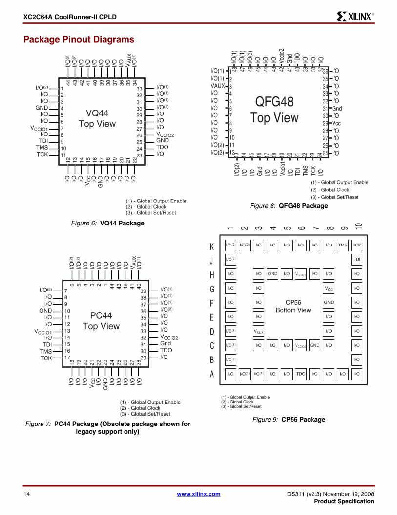
XC2C64A CoolRunner-II CPLD
14 wwwxilinxcom DS311 (v23) November 19 2008Product Specification
R
Package Pinout Diagrams
Figure 6 VQ44 Package
Figure 7 PC44 Package (Obsolete package shown for legacy support only)
VQ44Top View
IO(1)
IO(1)
IO(1)
IO(3)
IOIOIOVCCIO2GNDTDOIO
IO(2
)
IO(2
)
IO IO IO IO IO IO IO VA
UX
IO(1
)
IO IO IO VC
CIO
GN
DIO IO IO IO IO
IO(2)
IOIO
GNDIOIO
VCCIO1IOTDI
TMSTCK
1234567891011
12 13 14 15 16 17 18 19 20 21 22
3332313029282726252423
44 43 42 41 40 39 38 37 36 35 34
(1) - Global Output Enable(2) - Global Clock(3) - Global SetReset
PC44Top View
IO(1)
IO(1)
IO(1)
IO(3)
IOIOIOVCCIO2GndTDOIO
IO(2
)
IO(2
)
IO IO IO IO IO IO IO VA
UX
IO(1
)
IO IO IO VC
CIO
GN
DIO IO IO IO IO
IO(2)
IOIO
GNDIOIO
VCCIO1IOTDI
TMSTCK
7891011121314151617
18 19 20 21 22 23 24 25 26 27 28
3938373635343332313029
6 5 4 3 2 1 44 43 42 41 40
(1) - Global Output Enable(2) - Global Clock(3) - Global SetReset
Figure 8 QFG48 Package
Figure 9 CP56 Package
QFG48Top View
IOIOIOIOIOGndIOVccIOIOIOIO
IO(1
)IO
(1)
IO(3
)IO IO IO Vc
cio2
Gnd
TDO
IO IO IO
IO(2
)IO IO G
ndIO IO Vc
cio1
IO TDI
TMS
TCK
IO
IO(1)IO(1)VAUXIOIOIOIOIOIOIOIO(2)IO(2)
123456789101112 13 14 15 16 17 18 19 20 21 22 23 24
363534333231302928272625
48 47 46 45 44 43 42 41 40 39 38 37
(1) - Global Output Enable
(2) - Global Clock
(3) - Global SetReset
CP56Bottom View
IO(2) IO(2) IO IO IO IO IO IO TMS TCK
IO(2) TDI
IO IO GND IO VCCIO1 IO IO IO
IO IO VCC IO
IO IO GND IO
IO IO IO IO
IO(1) VAUX IO IO
IO(1) IO IO IO VCCIO2 GND IO IO
IO(3) IO
IO IO(1) IO(1) IO IO TDO IO IO IO IO
K
J
H
G
F
E
D
C
B
A
1 2 3 4 5 6 7 8 9 10
(1) - Global Output Enable(2) - Global Clock(3) - Global SetReset
XC2C64A CoolRunner-II CPLD
DS311 (v23) November 19 2008 wwwxilinxcom 15Product Specification
R
Warranty DisclaimerTHESE PRODUCTS ARE SUBJECT TO THE TERMS OF THE XILINX LIMITED WARRANTY WHICH CAN BE VIEWEDAT httpwwwxilinxcomwarrantyhtm THIS LIMITED WARRANTY DOES NOT EXTEND TO ANY USE OF THEPRODUCTS IN AN APPLICATION OR ENVIRONMENT THAT IS NOT WITHIN THE SPECIFICATIONS STATED ON THETHEN-CURRENT XILINX DATA SHEET FOR THE PRODUCTS PRODUCTS ARE NOT DESIGNED TO BE FAIL-SAFEAND ARE NOT WARRANTED FOR USE IN APPLICATIONS THAT POSE A RISK OF PHYSICAL HARM OR LOSS OFLIFE USE OF PRODUCTS IN SUCH APPLICATIONS IS FULLY AT THE RISK OF CUSTOMER SUBJECT TOAPPLICABLE LAWS AND REGULATIONS
Figure 12 VQ100 Package
VQ100Top View
GN
DIO
(3)
VC
CIO
2IO N
CN
CIO N
CIO IO IO IO V
CC
IO2
NC
NC
NC
GN
DT
DO
NC
IO NC
IO IO IO IO
VC
CIO
(2)
IO IO IOG
ND
IO IO IO IO IO IOV
CC
IO1
IO IO IO IO IO NC
TD
IN
CT
MS
TC
KIO IO
NCIONCIOIOIOGNDIOIONCNCIONCGNDIOIONCIOVccIOIONCIOIOVCCIO1
IO(1)
IO(1)
IO(1)
IO(1)
VAUXIOIOIOIOIOIOIOIOIOIOIOIOIOIONC
GNDIO(2)
IO(2)
IONC
12345678910111213141516171819202122232425
75747372717069686766656463626160595857565554535251
26 27 28 29 30 31 32 33 34 35 36 37 38 39 40 41 42 43 44 45 46 47 48 49 50
100 99 98 97 96 95 94 93 92 91 90 89 88 87 86 85 84 83 82 81 80 79 78 77 76
(1) - Global Output Enable(2) - Global Clock(3) - Global SetReset
XC2C64A CoolRunner-II CPLD
16 wwwxilinxcom DS311 (v23) November 19 2008Product Specification
R
Additional InformationAdditional information is available for the followingCoolRunner-II CPLD topics atwwwxilinxcomsupportdocumentationcoolrunner-iihtm
bull Device pinouts in the density specific data sheetsbull Termination power sequencing voltage thresholds
and slew rate data in the CPLD IO User Guide
bull Reliability data in the Device Reliability Reportbull Packaging thermal and electrical data in the Device
Package User Guide
Package drawings and dimensions are available atwwwxilinxcomsupportdocumentationpackage_specificationshtm
Revision HistoryThe following table shows the revision history for this document
Date Version Revision
51504 10 Initial Xilinx release
83004 11 Pb-free documentation
100104 12 Add Asynchronous PresetReset Pulse Width specification to AC Electrical Characteristics
110804 13 Product Release No change to documentation
112904 14 Change to QFG package drawing (Figure 8) Pin 29 relabelled
121404 15 Changes to Figure 4 Typical IO Output Curves Changes to tOUT25 and tOUT33 Internal Timing Parameters page 8
011805 16 Changes to ICCSB fTOGGLE tPSU1 tPSU2 tPHD tCW tSLEW25 and tSLEW33
030705 17 Format change to specifications IIL and IIH page 3 Improvement to pin-to-pin logic delay page 1 Modifications to Table 1 IOSTANDARDs
062805 18 Move to Product Specification Change to TIN25 TOUT25 TIN33 and TOUT33
013006 19 Modified footnote 1 from AC Specifications Table to remove incorrect equation
032006 20 Add Warranty Disclaimer Add note to Pin Descriptions that GCK GSR and GTS pins can also be used for general purpose IO
021507 21 Change to VIH specification for 25V and 18V LVCMOS Change TF specification on -7 speed grade from 20 to 30 ns
030807 22 Fixed typo in note for VIL for LVCMOS18 removed note for VIL for LVCMOS33
111908 23 Added note to Pin Description tables to indicate the PC44 packages are obsolete Removed part numbers for devices in PC44 packages the Features section and from the ordering information See Product Discontinuation Notice xcn07022pdf
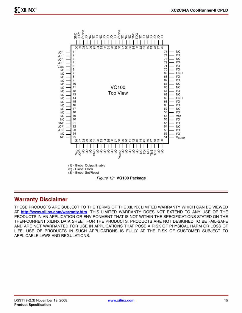
XC2C64A CoolRunner-II CPLD
16 wwwxilinxcom DS311 (v23) November 19 2008Product Specification
R
Additional InformationAdditional information is available for the followingCoolRunner-II CPLD topics atwwwxilinxcomsupportdocumentationcoolrunner-iihtm
bull Device pinouts in the density specific data sheetsbull Termination power sequencing voltage thresholds
and slew rate data in the CPLD IO User Guide
bull Reliability data in the Device Reliability Reportbull Packaging thermal and electrical data in the Device
Package User Guide
Package drawings and dimensions are available atwwwxilinxcomsupportdocumentationpackage_specificationshtm
Revision HistoryThe following table shows the revision history for this document
Date Version Revision
51504 10 Initial Xilinx release
83004 11 Pb-free documentation
100104 12 Add Asynchronous PresetReset Pulse Width specification to AC Electrical Characteristics
110804 13 Product Release No change to documentation
112904 14 Change to QFG package drawing (Figure 8) Pin 29 relabelled
121404 15 Changes to Figure 4 Typical IO Output Curves Changes to tOUT25 and tOUT33 Internal Timing Parameters page 8
011805 16 Changes to ICCSB fTOGGLE tPSU1 tPSU2 tPHD tCW tSLEW25 and tSLEW33
030705 17 Format change to specifications IIL and IIH page 3 Improvement to pin-to-pin logic delay page 1 Modifications to Table 1 IOSTANDARDs
062805 18 Move to Product Specification Change to TIN25 TOUT25 TIN33 and TOUT33
013006 19 Modified footnote 1 from AC Specifications Table to remove incorrect equation
032006 20 Add Warranty Disclaimer Add note to Pin Descriptions that GCK GSR and GTS pins can also be used for general purpose IO
021507 21 Change to VIH specification for 25V and 18V LVCMOS Change TF specification on -7 speed grade from 20 to 30 ns
030807 22 Fixed typo in note for VIL for LVCMOS18 removed note for VIL for LVCMOS33
111908 23 Added note to Pin Description tables to indicate the PC44 packages are obsolete Removed part numbers for devices in PC44 packages the Features section and from the ordering information See Product Discontinuation Notice xcn07022pdf
Recommended