The information contained in this document has been carefully researched and is, to the best of our
knowledge, accurate. However, we assume no liability for any product failures or damages, immediate or
consequential, resulting from the use of the information provided herein. Our products are not intended for
use in systems in which failures of product could result in personal injury. All trademarks mentioned herein
are property of their respective owners. All specifications are subject to change without notice.
Datasheet
ORTUSTECH
COM50H5N01ULC
OR-20-012

(1/33)
SPECIFICATIONS 16TLM034 Issue: Oct. 18, 2017
Specifications for
Blanview TFT-LCD Monitor (TENTATIVE)( 5.0" WVGA 800 x RGB x 480 Landscape)
Version 1.0(Please be sure to check the specifications latest version. )
MODEL COM50H5N01ULC
ORTUS TECHNOLOGY CO., LTD.
Approved by
Checked by
Prepared by
ORTUS TECHNOLOGY CO.,LTD.
Customer's Approval
Signature:
Name:
Section:
Title:
Date:
This product is under development andspecifications are subject to change.

(2/33)
SPECIFICATIONS 16TLM034 Issue: Oct. 18, 2017
Contents
1. Application ・・・・・・・・・ 32. Outline Specifications
2.1 Features of the Product ・・・・・・・・・ 42.2 Display Method ・・・・・・・・・ 4
3. Dimensions and Shape3.1 Dimensions ・・・・・・・・・ 63.2 Outward Form ・・・・・・・・・ 73.3 Serial Label (S-Label) ・・・・・・・・・ 8
4. Pin Assignment ・・・・・・・・・ 95. Absolute Maximum Rating ・・・・・・・・・ 106. Recommended Operating Conditions ・・・・・・・・・ 107. Electrical Characteristics
7.1 DC Characteristics ・・・・・・・・・ 107.2 3-wire Serial interface ・・・・・・・・・ 127.3 LVDS interface ・・・・・・・・・ 137.4 Input timing ・・・・・・・・・ 167.5 Power ON/OFF sequence ・・・・・・・・・ 17
8. LED Circuit ・・・・・・・・・ 189. Characteristics
9.1 Optical Characteristics ・・・・・・・・・ 199.2 Temperature Characteristics ・・・・・・・・・ 20
10 Criteria of Judgment10.1 Defective Display and Screen Quality ・・・・・・・・・ 2110.2 Screen and Other Appearance ・・・・・・・・・ 22
11. Reliability Test ・・・・・・・・・ 2312. Packing Specifications ・・・・・・・・・ 2513. Handling Instruction
13.1 Cautions for Handling LCD panels ・・・・・・・・・ 2613.2 Precautions for Handling ・・・・・・・・・ 2713.3 Precautions for Operation ・・・・・・・・・ 2713.4 Storage Condition for Shipping Cartons ・・・・・・・・・ 2813.5 Precautions for Peeling off ・・・・・・・・・ 29
the Protective film 13.6 Warranty ・・・・・・・・・ 29
APPENDIX ・・・・・・・・・ 30
ORTUS TECHNOLOGY CO.,LTD.

(3/33)
SPECIFICATIONS 16TLM034 Issue: Oct. 18, 2017
1. Application
This Specification is applicable to 127.3mm (5.0 inch) Blanview TFT-LCD monitor for non-military use.
ORTUS TECHNOLOGY makes no warranty or assume no liability that use of this Product and/or any information
including drawings in this Specification by Purchaser is not infringing any patent or other intellectual
property rights owned by third parties, and ORTUS TECHNOLOGY shall not grant to Purchaser any right to use
any patent or other intellectual property rights owned by third parties. Since this Specification contains
ORTUS TECHNOLOGY's confidential information and copy right, Purchaser shall use them with high degree of
care to prevent any unauthorized use, disclosure, duplication, publication or dissemination of
ORTUS TECHNOLOGY'S confidential information and copy right.
If Purchaser intends to use this Products for an application which requires higher level of reliability
and/or safety in functionality and/or accuracy such as transport equipment
(aircraft, train, automobile, etc.), disaster-prevention/security equipment or various safety
equipment, Purchaser shall consult ORTUS TECHNOLOGY on such use in advance.
This Product shall not be used for application which requires extremely higher level of
reliability and/or safety such as aerospace equipment, telecommunication equipment for trunk lines,
control equipment for nuclear facilities or life-support medical equipment.
It must be noted as an mechanical design manner, especial attention in housing design to prevent
arcuation/flexureor caused by stress to the LCD module shall be considered.
ORTUS TECHNOLOGY assumes no liability for any damage resulting from misuse, abuse, and/or
miss-operation of the Product deviating from the operating conditions and precautions
described in the Specification.
It shall be mutually conferred if nonconforming defect
which result from unspecified cause in this specification arises.
If any issue arises as to information provided in this Specification or any other information,
ORTUS TECHNOLOGY and Purchaser shall discuss them in good faith and seek solution.
ORTUS TECHNOLOGY assumes no liability for defects such as electrostatic discharge failure occurred
during peeling off the protective film or Purchaser's assembly process.
This Product is compatible for RoHS directive.
Object substance Maximum content [ppm]
Cadmium and its compound 100
Hexavalent Chromium Compound 1000
Lead & Lead compound 1000
Mercury & Mercury compound 1000
Polybrominated biphenyl series(PBB series) 1000
Polybrominated biphenyl ether series(PBDE series) 1000
ORTUS TECHNOLOGY CO.,LTD.

(4/33)
SPECIFICATIONS 16TLM034 Issue: Oct. 18, 2017
2. Outline Specifications
2.1 Features of the Product
- 5.0 inch diagonal display, 800 x RGB [H] x 480 [V] dots.
- 16.7 M colors (8-bit) / 262 K colors (6-bit).
- 3.3V voltage single power source.
- Timing generator [TG], Counter-electrode driving circuitry, Built-in power supply circuit.
- Long life & High bright white LED back-light.
- Blanview TFT-LCD, improved outdoor readability.
Readability Power Efficiency Readability Power Efficiency
(Battery Life) (Battery Life)
2.2 Display Method
Items Specifications Remarks
Display type VA 16.7 M colors. / 262 K colors.
Blanview, Normally black.
Driving method a-Si TFT Active matrix.
Line-scanning, Non-interlace.
Dot arrangement RGB stripe arrangement. Refer to "Dot arrangement"
Signal input method 8-bit / 6-bit LVDS interface (VESA format)
Backlight type Long life & High bright white LED.
NTSC ratio 50%
Active area
X1 X2 ・ ・ ・ ・ ・ X799 X800
1 2 3 4 2397 2398 2399 2400
・ ・ ・ ・
・ ・ ・ ・ Active area
・ ・ ・ ・
Dot arrangement (FPC cable placed down side)
ORTUS TECHNOLOGY CO.,LTD.
B・ B R G
Poor
Transflective Fair Poor Good Good
Transmissive Good Good Fair
Blanview Good Good Good Good
Y1 R G B R ・ ・ ・ ・ ・ B R G B
Y2 R G B R ・ ・ ・ ・ ・ B R G B
Y479 R G B R ・ ・ ・ ・ ・ B R G B
Y480 R G B R ・ ・ ・ ・
Indoor Outdoor
A
(5/33)
SPECIFICATIONS 16TLM034 Issue: Oct. 18, 2017
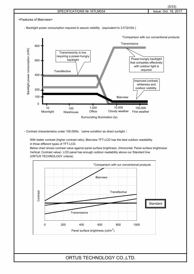
<Features of Blanview>
- Backlight power consumption required to assure visibility. (equivalent to 3.5”QVGA )
- Contrast characteristics under 100,000lx. (same condition as direct sunlight.)
With better contrast (higher contrast ratio), Blanview TFT-LCD has the best outdoor readability
in three different types of TFT-LCD.
Below chart shows contrast value against panel surface brightness. (Horizontal: Panel surface brightness/
Vertical: Contrast value) LCD panel has enough outdoor readability above our Standard line. (ORTUS TECHNOLOGY criteria)
CRパネル輝度 Blanview 半透過 透過型 OKライン
0 1.125 0.875 0.375 1.00
100 1.00
200 1.00
300 2 1.00
400 1.125 1.00
500 1.00
600 1.00
700 1.00
800 1.00
900 1.00
1000 1.25 1.00
ORTUS TECHNOLOGY CO.,LTD.
0 200 400 600 800 1000
Panel surface brightness (cd/m2)
Co
ntr
ast
Blanview
Transmissive
Transflective
*Comparison with our conventional products
Standard
0
400
800
Surrounding illumination (lx)
Blanview
Transmissive
Transflective
100
200
600
*Comparison with our conventional products
Transmissivity is low,requiring a power-hungry
backlight Power-hungry backlightthat competes effectively
with outdoor light isrequired.
Improved contrast,whiteness and
outdoor visibility.
100,000Fine weather
10,000Cloudy weather
1,000Office
100Warehouse
10Moonlight
Ba
cklig
ht
po
we
r co
nsu
mp
tion
(m
W)

(6/33)
SPECIFICATIONS 16TLM034 Issue: Oct. 18, 2017
3. Dimensions and Outward Form
3.1 Dimensions
Items Specifications Unit Remarks
Outline dimensions 124.00[H] × 80.82[V] ×6.18[D] mm Exclude FPC cable and
parts on FPC.Active area 109.20[H] × 65.52[V] mm 127.3mm diagonal
Number of dots 2400[H] × 480[V] dot
Dot pitch 45.5[H] × 136.5[V] um
Surface hardness of the polarizer 2 H Load:2.94N
Weight 88 g Include FPC cable
ORTUS TECHNOLOGY CO.,LTD.
A

3.2 Outward Form
(7/33)16TLM034
Issue:Oct.18,2017

(8/33)
SPECIFICATIONS 16TLM034 Issue: Oct. 18, 2017
3.3 SERIAL LABEL (S-LABEL)
1) Display Items
A section : Bar codeB section : Combination of a character
A section
B section * * * * * * * 0 0 0 1 2 5C O M 5 0 H 5 N 0 1 U L C
Details of B section
Upper column: It indicates The least significant digit of manufacture year (1 digit),manufacture month with below alphabet (1letter), model code (5characters),
serial number (6digits).
* * ***** ******
a b
Contents of display
a The least significant digit of manufacture year
b Manufacture month Jan-A Mar-C May-E Jul-G Sep-I Nov-K
Feb-B Apr-D Jun-F Aug-H Oct-J Dec-L
c Model code 50BRC (Made in Japan)50BSC (Made in Malaysia)
d Serial number
* Example of indication of Serial label (S-label)
・Made in Japan ・Made in Malaysia
means "manufactured in October 2017, 5.0" BR type, means "manufactured in October 2017, 5.0" BS type,
C specifications, serial number 000125" C specifications, serial number 000125"
Lower column: Model (13characters)
2) Location of Serial Label (S-label)
Refer to 3.2 "Outward Form".
2) Others
Bar code readability is excluded from quality assurance coverage.
ORTUS TECHNOLOGY CO.,LTD.
c d
7J50BRC000125 7J5BSC000125
A
(9/33)
SPECIFICATIONS 16TLM034 Issue: Oct. 18, 2017
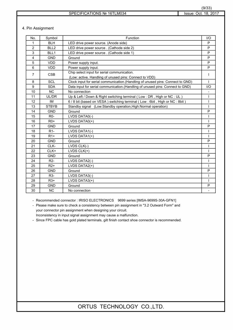
4. Pin Assignment
No. Symbol Function I/O
1 BLH LED drive power source. (Anode side) P
2 BLL2 LED drive power source . (Cathode side 2) P
3 BLL1 LED drive power source . (Cathode side 1) P
4 GND Ground P
5 VDD Power supply input. P
6 VDD Power supply input. PChip select input for serial communication.
(Low: active. Handling of unused pins: Connect to VDD)8 SCL Clock input for serial communication.(Handling of unused pins: Connect to GND) I
9 SDA Data input for serial communication.(Handling of unused pins: Connect to GND) I/O
10 NC No connection -
11 UL/DR Up & Left / Down & Right switching terminal ( Low : DR , High or NC : UL ) I
12 IM 6 / 8 bit (based on VESA ) switching terminal ( Low : 6bit , High or NC : 8bit ) I
13 STBYB Standby signal (Low:Standby operation,High:Normal operation) I
14 GND Ground P
15 R0- LVDS DATA0(-) I
16 R0+ LVDS DATA0(+) I
17 GND Ground P
18 R1- LVDS DATA1(-) I
19 R1+ LVDS DATA1(+) I
20 GND Ground P
21 CLK- LVDS CLK(-) I
22 CLK+ LVDS CLK(+) I
23 GND Ground P
24 R2- LVDS DATA2(-) I
25 R2+ LVDS DATA2(+) I
26 GND Ground P
27 R3- LVDS DATA3(-) I
28 R3+ LVDS DATA3(+) I
29 GND Ground P
30 NC No connection -
- Recommended connector : IRISO ELECTRONICS 9699 series [IMSA-9699S-30A-GFN1]
- Please make sure to check a consistency between pin assignment in "3.2 Outward Form" and
your connector pin assignment when designing your circuit.
Inconsistency in input signal assignment may cause a malfunction.
- Since FPC cable has gold plated terminals, gilt finish contact shoe connector is recommended.
ORTUS TECHNOLOGY CO.,LTD.
7 CSB I

(10/33)
SPECIFICATIONS 16TLM034 Issue: Oct. 18, 2017
5. Absolute Maximum RatingGND=0V
Rating
MIN MAX
UL/DR , IM , SCL , CSB ,
SDA , STBYB
6. Recommended Operating ConditionsGND=0V
Rating
MIN TYP MAX
UL/DR , IM , SCL , CSB ,
SDA , STBYB
Note1 Panel surfacetemperature
Note1: This monitor is operatable in this temperature range. With regard to optical characteristics,
refer to Item 9."CHARACTERISTICS".
7. Electrical Characteristics
7.1 DC Characteristics(Unless otherwise noted, Ta=25 ,VDD=3.3V,GND=0V)
Rating
MIN TYP MAX
UL/DR,IM,
SCL,CSB,SDA,
STBYB
IOH=-400uA
IOL=400uA
Color Bar
fclk = 27.2 MHz
ORTUS TECHNOLOGY CO.,LTD.
SDA
V
Operational temperaturerange
Top -30 25 85
Item Symbol
3.63.33.0
Input voltage for logic VI 0 -- VDD
BLH-BLL1/BLL2
Supply voltage
Item Symbol
VDD
Condition Unit Applicable terminal
VDDV
-40 95
VI
VDDSupply voltage
Input voltage for logic
Forward current IL
Storage temperature range
Tstg
mA
3.9-0.3
-0.3 VDD+0.3
-- (70.0)
Applicable terminal
VDDV
V
Item Symbol Condition Unit
Condition Unit Applicable terminal
VIH 0.7VDD - VDD V
V
VOH VDD-0.4 - VDD V
VIL 0 - 0.3VDD
VOL 0 - 0.4 V
Pull up/downresistor
RI
200 350 850 kΩ
100 175 425
Pull downSCL , SDA
200 350 850 kΩPull up :IM , CSB , STBYB
kΩPull up :UL/DR
OperatingCurrent
IDD - (34.1) (68.2) mA VDD
High Level InputVoltage
Low Level InputVoltage
High LevelOutput Voltage
Low LevelOutput Voltage
A
A

(11/33)
SPECIFICATIONS 16TLM034 Issue: Oct. 18, 2017
( Back Light )
Rating
MIN TYP MAX
Ta=25 IL=(34.0) mA Note1
Ta=25 IL=(34.0) mA Note2
Note1: - Reference value
Note2: - The lifetime of the LED is defined as a period till the brightness of the LED
decreases to the half of its initial value.
- This figure is given as a reference purpose only, and not as a guarantee.
- This figure is estimated for an LED operating alone.
As the performance of an LED may differ when assembled as a monitor
together with a TFT panel due to different environmental temperature.- Estimated lifetime could vary on a different temperature and usually
higher temperature could reduce the life significantly.
ORTUS TECHNOLOGY CO.,LTD.
Applicable terminalUnitItem Symbol Condition
Forward current
Forward voltage
Estimated Life ofLED
IL
LL
mA BLH - BLL1 / BLL2
VL -- V
Ta=25 -- (34.0) (70.0)
hrs--
(14.3)
( 100000 ) --
(16.3)
A

(12/33)
SPECIFICATIONS 16TLM034 Issue: Oct. 18, 2017
7.2 3-wire Serial interface
AC Characteristics(Unless otherwise noted, Ta=25 ,VDD=3.3V,GND=0V)
Rating Applicable terminal
MIN TYP MAX
Serial clock cycle fSCL - - 6.7 MHz SCL
Clock duty ratio - 40 50 60 %
CSB
CSB to SCL SCL、CSB、SDA
SDA to SCL
CSB to SCL
SDA to SCL
SCL to SDO Read :
SCL to SDO SCL、CSB、SDA
Write timing
1 2 3 4 5 6 7 8 9 10 11 12 13 14 15 16
ORTUS TECHNOLOGY CO.,LTD.
Item Symbol Condition Unit
SCL High pulse width TW1H 75 --
-- μs
SCL Low pulse width TW1L 75 --
-- ns
-- ns
-- ns
CSB pulse width TW2
CSB setup time TS0 60 --
1 --
SDA setup time TS1 60 --
-- ns
CSB hold time TH0 60 --
-- ns
-- ns
( 50 ) ns
SDA hold time TH1
Output access time TACC ( 5 ) --
60 --
( 50 ) nsOutput hold time TDH ( 5 ) --
CSB
SDA
SCL
Write Register address Register data
ID0
D0D1D2D3D4D5D6D7A0A1A2A3A4A5R/W
0
ID
CSB
SDA
SCL
TW2TH0
TS0
TS1 TH1
TW1H TW1L
70%
30%
30%
70%
30% 30%
70%
30%
70%SDA(Read)
TACC TDH
30%
70%
70%
(13/33)
SPECIFICATIONS 16TLM034 Issue: Oct. 18, 2017
7.3 LVDS interface
7.3.1 LVDS DC Characteristics(Unless otherwise noted, Ta=25 ,VDD=3.3V,GND=0V)
Rating
MIN TYP MAXRXVCM=1.2V CLK+、CLK-
R0+、R0-、R1+、R1-
R2+、R2-、R3+、R3-
ORTUS TECHNOLOGY CO.,LTD.
Differential inputvoltage
Differential inputleakage current
Item
Differential input highthreshold voltage
Differential input lowthreshold voltage
Differential inputcommon Mode voltage
Symbol Condition Unit Applicable terminal
Rxvth
Rxvtl
Rxvcm
|VID|
RVleak
- - 0.1
-0.1 - -
1.0 1.2 1.4
0.2 - 0.6
-10 - +10 μA
V
V
V
V
Rxvcm
GND
LVx-
LVx+
- |VID|
(LVX+) - (LVX-) = - |VID| < Rxvtl = "Low"
(LVX+) -( LVX-) = |VID| > Rxvth = "High"
Rxvtl
Rxvth |VID|
|VID|
Single end signals
Differential signals

(14/33)
SPECIFICATIONS 16TLM034 Issue: Oct. 18, 2017
7.3.2 LVDS AC Characteristics(Unless otherwise noted, Ta=25 ,VDD=3.3V,GND=0V)
Rating
MIN TYP MAX
25.2 27.2 30.5
32.8 36.8 39.7
- 1/7 -
2.9 4 4.1
2.9 3 4.1
-0.2 0 0.2
0.8 1 1.2
1.8 2 2.2
2.8 3 3.2
3.8 4 4.2
4.8 5 5.2
5.8 6 6.2
0.6 - -
- - 0.2
Tpos_1
Tpos_0
Tpos_6
Tpos_5
Tpos_4
Tpos_3
Tpos_2
ORTUS TECHNOLOGY CO.,LTD.
Unit
CLK Frequency f clk MHz
Item Symbol
Clock period Tc ns
1 data bit time UI Tc
CLK High level Width T chw UI
CLK Low level Width T clw UI
Position 1 Tpos_1 UI
Position 0 Tpos_0 UI
Position 6 Tpos_6 UI
Position 5 Tpos_5 UI
Position 4 Tpos_4 UI
Position 3 Tpos_3 UI
UI
CLK+
Position 2 Tpos_2 UI
Reciever Strobe Position 7 TEYEW UI
R0~R3+/-
R0~R3+/-
Reciever Strobe Position 8 TEX
1 CLK = Tc
T chw T clw
Rx_1 Rx_6 Rx_5 Rx_4 Rx_3 Rx_2 Rx_1 Rx_0 Rx_6 Rx_5Rx_0Rx_2
1 data bit time ( UI )
TEYEWTEX TEX
Rxvcm
Rxvcm + 0.5RxvthRxvcm - 0.5Rxvtl
Rxvcm - 0.5RxvthRxvcm + 0.5Rxvtl

(15/33)
SPECIFICATIONS 16TLM034 Issue: Oct. 18, 2017
7.3.3 LVDS Data Format
VESA Format 8bit * ( MSB : R[7],G[7],B[7] )
CLK+
CLK-
R0+
R0-
R1+
R1-
R2+
R2-
R3+
R3-
VESA Format 6bit * ( MSB : R[5],G[5],B[5] )
CLK+
CLK-
R0+
R0-
R1+
R1-
R2+
R2-
R3+
R3-
ORTUS TECHNOLOGY CO.,LTD.
R[1] R[0] G[0] R[5] R[4] R[3] R[2] R[1] R[0] G[0]
G[2] G[1] B[1] B[0] G[5] G[4] G[3] G[2] G[1] B[1]
B[3] B[2] ENAB VD HD B[5] B[4] B[3] B[2] ENAB
R[7] R[6] - B[7] B[6] G[7] G[6] R[7] R[6] -
R[1] R[0] G[0] R[5] R[4] R[3] R[2] R[1] R[0] G[0]
G[2] G[1] B[1] B[0] G[5] G[4] G[3] G[2] G[1] B[1]
B[3] B[2] ENAB VD HD B[5] B[4] B[3] B[2] ENAB
- - - - - - - - - -
Current cycle Next cyclePrevious cycle
Current cycle Next cyclePrevious cycle

(16/33)
SPECIFICATIONS 16TLM034 Issue: Oct. 18, 2017
7.4 Input timing
CLK frequency fCLK 25.2 27.2 30.5 MHz CLK
VD frequency fVD 60 Hz VD
1 vertical field tv 490 528 552 H
VD pulse width tvp 1 2 66 H
VD back porch tvb 5 10 67 H VD,HD,ENAB
VD front porch tvf 5 38 67 H R[7:0],G[7:0],B[7:0]
Vertical valid data tvdp 480 H
HD frequency fHD 28.8 kHz HD
1 horizontal field th 856 860 920 CLK
HD pulse width thp 1 2 100 CLK
HD back porch thb 5 16 101 CLK CLK,HD,ENAB
HD front porch thf 19 44 115 CLK R[7:0],G[7:0],B[7:0]
ENAB pulse width tenp 800 CLK
Horizontal valid data thdp 800 CLK
( * ) Input terminals are (R0+/- , R1+/- , R2+/- , R3+/- , CLK+/-).
<Vertical timing>
VD
HD
ENAB
RGB
<Horizontal timing>
HD
CLK
ENAB
RGB
ORTUS TECHNOLOGY CO.,LTD.
X1 ** * * * * * * * * * * ** * * ** * * *
X79
9X
800
* *
X79
7X
798
X2
X3
X4
Unit Signal ( * )Item SymbolRating
MIN TYP MAX
Y1
Y2
Y3
Y4
Y47
8
Y47
9
Y48
0
t v
t vp 1H
t vb t vdp t vf
t h
t hp
t hb t enp t hf
t hdp

(17/33)
SPECIFICATIONS 16TLM034 Issue: Oct. 18, 2017
7.5 Power ON/OFF sequence
0.5 ~ 10 ms
VDD
10 us ~ 2ms
RESETB
(Internal)
>20 ms > 0 ms
STBYB
> 0 ms > 84 ms
CLK+/CLK-
R0+/R0-、R1+/R1-
R2+/R2-、R3+/R3-
ENAB
HD
1 2 3 4 5 6 7
VD
Black Normal Normal Black Display disp disp disp disp
Auto Power on sequence
Note: ENAB, HD and VD are included in the R2 + / R2- terminals.
ORTUS TECHNOLOGY CO.,LTD.
2.7v
A

(18/33)
SPECIFICATIONS 16TLM034 Issue: Oct. 18, 2017
8. LED Circuit
BLH
IL
BLL1
IL
BLL2
A K
ESD Protection Device
ORTUS TECHNOLOGY CO.,LTD.

(19/33)
SPECIFICATIONS 16TLM034 Issue: Oct. 18, 2017
9. Characteristics
9.1 Optical Characteristics < Measurement Condition >
Measuring instruments: CS2000(KONICA MINOLTA), LCD7200(OTSUKA ELECTRONICS),
EZcontrast160D(ELDIM)
Driving condition: VDD = 3.3V, VSS = 0V
Optimized VCOMDC
Backlight: IL=34.0mA
Measured temperature: Ta=25゜C
Item Symbol Condition MIN TYP MAX Unit Remark
TON [Data]= - - (60) ms 1
00h→FFh
TOFF [Data]= - - (40) ms
FFh→00h
CR [Data]= ( 540 ) ( 900 ) - 2
FFh / 00h
- ( 1.7 ) -
Left θL [Data]= ( 80 ) - - deg 3
Right θR FFh / 00h ( 80 ) - - deg
Up φU CR≧10 ( 80 ) - - deg
Down φD ( 80 ) - - deg
x [Data]=FFh 4
y
5
Center brightness [Data]=FFh (250) ( 400 ) - cd/m2 6
Brightness distribution [Data]=FFh ( 70 ) - - % 7
* Note number 1 to 7: Refer to the APPENDIX of "Reference Method for Measuring Optical Characteristics".
ORTUS TECHNOLOGY CO.,LTD.
White Chromaticity White chromaticity range
Burn-inNo noticeable burn-in image shall
be observed after 2 hours ofwindow pattern display.
Note No.
Res
pons
etim
eV
iew
ing
an
gle
Co
ntr
ast
ratio
Backlight ON
Backlight OFF
Rise time
Fall time
A

(20/33)
SPECIFICATIONS 16TLM034 Issue: Oct. 18, 2017
【White Chromaticity Range】
Ta=25゜C0.26 0.33
0.26 0.26
0.33 0.26
0.35 0.30
0.35 0.36
0.34 0.37
0.28 0.37
White Chromaticity Range
9.2 Temperature Characteristics
< Measurement Condition >
Measuring instruments: CS2000(KONICA MINOLTA), LCD7200(OTSUKA ELECTRONICS)
Driving condition: VDD = 3.3V, VSS = 0V
Optimized VCOMDC
Backlight: IL=34.0mA
Ta=-20°C
(200) or more (200) or more Backlight ON
(200) msec or less (30) msec or less
(300) msec or less (50) msec or less
ORTUS TECHNOLOGY CO.,LTD.
x y
ItemSpecification
RemarkTa=70゜C
Contrast ratio CR
Display QualityNo noticeable display defect or ununiformityshould be observed.
Response time
Rise time TON
Fall time TOFF
0.22
0.24
0.26
0.28
0.30
0.32
0.34
0.36
0.38
0.40
0.22 0.24 0.26 0.28 0.30 0.32 0.34 0.36 0.38 0.40
x
y
A
A

(21/33)
SPECIFICATIONS 16TLM034 Issue: Oct. 18, 2017
10. Criteria of Judgment
10.1 Defective Display and Screen Quality
Test Condition: Observed TFT-LCD monitor from front during operation
with the following conditions
Driving Signal Raster Patter (RGB, white, black)
Signal condition [Data]:00h, A8h, FFh (3steps)
Observation distance 30 cm
Illuminance 200 to 350 lx
Backlight IL=34.0mA
Defect item Defect content Criteria
Black, white or color line, 3 or more neighboring defective dots Not exists
Uneven brightness on dot-by-dot base due to defective Refer to table 1
TFT or CF, or dust is counted as dot defect
(brighter dot, darker dot)
High bright dot: Visible through 2% ND filter at [Data]=00h
Low bright dot: Visible through 5% ND filter at [Data]=00h
Dark dot: Appear dark through white display at [Data]=A8h
Invisible through 5% ND filter at [Data]=00h Acceptable
Uneven brightness (white stain, black stain etc) Invisible through 5% ND filter at Black screen.
Invisible through 1% ND filter at other screen.
Point-like 0.25mm< φ N=0
0.20mm< φ ≦0.25mm N≦3
φ ≦0.20mm Acceptable
Liner 3.0mm<length and 0.08mm<width N=0
length≦3.0mm or width≦0.08mm Acceptable
Use boundary sample
for judgment when necessary
φ(mm): Average diameter = (major axis + minor axis)/2
Permissible number: N
Table 1
High Low Dark
Area bright bright dot Total Criteria
dot dot
A 0 2 2 3 Permissible distance between same color bright dots
(includes neighboring dots): 3 mm or more
B 2 4 4 6 Permissible distance between same color high bright dots
(includes neighboring dots): 5 mm or more
Total 2 4 4 7
<Landscape model>
B zone Division of A and B areas
B area: Active area
A zone Dimensional ratio between A and B areas: 1: 4: 1
(Refer to the left figure)
1 4 1
ORTUS TECHNOLOGY CO.,LTD.
1
4
1
Dis
pla
y Q
ua
lity
Dotdefect
Scr
ee
n Q
ua
lity
Dirt
Foreignparticle
Others
Linedefect
90°
30cm

(22/33)
SPECIFICATIONS 16TLM034 Issue: Oct. 18, 2017
10.2 Screen and Other AppearanceTesting conditions
Observation distance 30cm
Illuminance 1200~2000 lx
Item Criteria Remark
Flaw Ignore invisible defect when the backlight is on. Applicable area:
Stain Active area only
Bubble (Refer to the section
Dust 3.2 "Outward form")
DentS-case No functional defect occurs
FPC cable No functional defect occurs
ORTUS TECHNOLOGY CO.,LTD.
Po
lari
zer

(23/33)
SPECIFICATIONS 16TLM034 Issue: Oct. 18, 2017
11. Reliability Test
number of failures
/number of examinations
Ta=95゜C 240hrs 0/3Ta=-40゜C 240hrs 0/3Ta=60゜C,RH=90% 240hrs 0/3non condensing ※
Tp=85゜C 240hrs 0/3Tp=-30゜C 240hrs 0/3Tp=40゜C,RH=90% 240hrs 0/3non condensing ※
-40←→95゜C(30min/30min) 100 cycles 0/3Confirms to EIAJ ED-4701/300 0/3C=200pF,R=0Ω,V=±200V
Each 3 times of discharge on and power supply
and other terminals.
C=250pF, R=100Ω, V=±12kV 0/3Each 5 times of discharge in both polarities
on the center of screen with the case grounded.
Pull the FPC with the force of 3N for 10 sec. 0/3in the direction - 90-degree to its
original direction.
Pull the FPC with the force of 3N for 10 sec. 0/3in the direction -180-degree to its
original direction. Reciprocate it 3 times.
Total amplitude 1.5mm, f=10~55Hz, X,Y,Z 0/3directions for each 2 hours
Use ORTUS TECHNOLOGY original jig 0/3(see next page)and make an impact with
peak acceleration of 1000m/s2 for 6 msec with
half sine-curve at 3 times to each X, Y, Z directions
in conformance with JIS C 60068-2-27-2011.
Acceleration of 19.6m/s2 with frequency of 0/1 Packing
10→55→10Hz, X,Y, Zdirection for each
30 minutes
Drop from 75cm high. 0/1 Packing
1 time to each 6 surfaces, 3 edges, 1 corner
Note:Ta=ambient temperature Tp=Panel temperature
※ The profile of high temperature/humidity storage and High Temperature/humidity operation
(Pure water of over 10MΩ・cm shall be used.)
ORTUS TECHNOLOGY CO.,LTD.
Impact test
Pa
ckin
g t
est
Packing vibration-proof test
Packing drop test
Me
cha
nic
al e
nvi
ron
me
nta
l te
st
Electrostatic discharge test(Non operation)
Surface discharge test(Non operation)
Vibration test
FPC tension test
FPC bend test
Test item Test conditionD
ura
bili
ty t
est
High temperature storage
Low temperature storage
High temperature & highhumidity storage
High temperature operation
Low temperature operation
High temp & humid operation
Thermal shock storage
storage:60operation:40
ordinarytemperature 90%RH
0h
0.5
h
1h
24
1h
24
1.5
h
24
2h
ordinaryhumidity
25
75%RH
60%RH
temperature
relative humidity
A
(24/33)
SPECIFICATIONS 16TLM034 Issue: Oct. 18, 2017
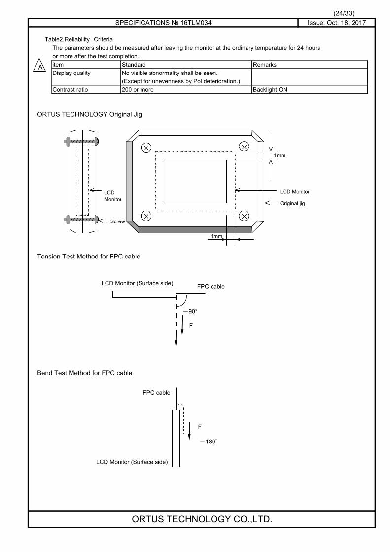
Table2.Reliability Criteria
The parameters should be measured after leaving the monitor at the ordinary temperature for 24 hours
or more after the test completion.
item Standard Remarks
Display quality No visible abnormality shall be seen.
(Except for unevenness by Pol deterioration.)
Contrast ratio 200 or more Backlight ON
ORTUS TECHNOLOGY Original Jig
Tension Test Method for FPC cable
Bend Test Method for FPC cable
ORTUS TECHNOLOGY CO.,LTD.
1mm
1mm
LCD Monitor
Original jig
Screw
LCDMonitor
LCD Monitor (Surface side)
-180゜
F
FPC cable
-90°
LCD Monitor (Surface side) FPC cable
F
A

(25/33)
SPECIFICATIONS 16TLM034 Issue: Oct. 18, 2017
12. Packing Specifications
ORTUS TECHNOLOGY CO.,LTD.
TBD

(26/33)
SPECIFICATIONS 16TLM034 Issue: Oct. 18, 2017
13. Handling Instruction13.1 Cautions for Handling LCD panels
Caution
(1) Do not make an impact on the LCD panel glass because it may break and you may get injured from it.
(2) If the glass breaks, do not touch it with bare hands.
(Fragment of broken glass may stick you or you cut yourself on it.
(3) If you get injured, receive adequate first aid and consult a medial doctor.
(4) Do not let liquid crystal get into your mouth.
(If the LCD panel glass breaks, try not let liquid crystal get into your mouth even toxic property
of liquid crystal has not been confirmed.)
(5) If liquid crystal adheres, rinse it out thoroughly.
(If liquid crystal adheres to your cloth or skin, wipe it off with rubbing alcohol or wash
it thoroughly with soap. If liquid crystal gets into eyes, rinse it with clean water
for at least 15 minutes and consult an eye doctor.
(6) If you scrap this products, follow a disposal standard of industrial waste
that is legally valid in the community, country or territory where you reside.
(7) Do not connect or disconnect this product while its application products is powered on.
(8) Do not attempt to disassemble or modify this product as it is precision component.
(9) If a part of soldering part has been exposed, and avoid contact (short-circuit) with a metallic part of the case etc. about FPC of this model, please.
Please insulate it with the insulating tape etc. if necessary.
The defective operation is caused, and there is a possibility to generation of heat and the ignition.
(10) Since excess current protection circuit is not built in this TFT module, there is the possibility that LCD module or peripheral circuit become feverish and burned in case abnormal operation is generated.
We recommend you to add excess current protection circuit to power supply.
(11) The devices on the FPC are damageable to electrostatic discharge,
because the terminals of the devices are exposed.Wear grounded wrist-straps and use electrostatic neutralization blowers to prevent static
charge and discharge when handling the TFT monitors.
Designate an appropriate operating area, and set equipment, tools, and machines properly
when handling this product.
Caution This mark is used to indicate a precaution or an instruction which,
if not correctly observed, may result in bodily injury, or material damages alone.
ORTUS TECHNOLOGY CO.,LTD.
!
!

(27/33)
SPECIFICATIONS 16TLM034 Issue: Oct. 18, 2017
13.2 Precautions for Handling
1) Wear finger tips at incoming inspection and for handling the TFT monitors to keep
display quality and keep the working area clean.
Do not touch the surface of the monitor as it is easily scratched.
2) Wear grounded wrist-straps and use electrostatic neutralization blowers to prevent static charge and discharge
when handling the TFT monitors as the LED in this TFT monitors is damageable to electrostatic discharge.
Designate an appropriate operating area, and set equipment, tools, and machines properly
when handling this product.
3) Avoid strong mechanical shock including knocking, hitting or dropping to the TFT monitors
for protecting their glass parts. Do not use the TFT monitors that have been experienced
dropping or strong mechanical shock.
4) Do not use or storage the TFT monitors at high temperature and high humidity environment.
Particularly, never use or storage the TFT monitors at a location where condensation builds up.
5) Avoid using and storing TFT monitors at a location where they are exposed to direct
sunlight or ultraviolet rays to prevent the LCD panels from deterioration by ultraviolet rays.
6) Do not stain or damage the contacts of the FPC cable .
FPC cable needs to be inserted until it can reach to the end of connector slot.
During insertion, make sure to keep the cable in a horizontal position to avoid an oblique insertion.
Otherwise, it may cause poor contact or deteriorate reliability of the FPC cable.
7) Do not bend or pull the FPC cable or carry the TFT monitor by holding the FPC cable.
Especially, it will cause mechanical damage or critical defect if FPC is pull up or bent up to short of display.
8) Peel off the protective film on the TFT monitors during mounting process.
Refer to the section 13.5 on how to peel off the protective film.
We are not responsible for electrostatic discharge failures or other defects
occur when peeling off the protective film.
13.3 Precautions for Operation
1) Since this TFT monitors are not equipped with light shielding for the driver IC,
do not expose the driver IC to strong lights during operation as it may cause functional failures.
2) In case of powering up or powering off this LCD module, be sure to comply the sequence as instructed in this specification.
3) Do not plug in or out the FPC cable while power supply is switch on.
Plug the FPC cable in and out while power supply is switched off.
4) Do not operate the TFT monitors in the strong magnetic field. It may break the TFT monitors.
5) Do not display a fixed image on the screen for a long time.Use a screen-saver or other measures to avoid a fixed image displayed on the screen for a long time.
Otherwise, it may cause burn-in image on the screen due the characteristics of liquid crystal.
ORTUS TECHNOLOGY CO.,LTD.
DO NOT BEND UP
FPC
Monitor

(28/33)
SPECIFICATIONS 16TLM034 Issue: Oct. 18, 2017
13.4 Storage Condition for Shipping Cartons
Storage environment
・ Temperature 0 to 40゜C
・ Humidity 60%RH or less
No-condensing occurs under low temperature with high humidity condition.
・ Atmosphere No poisonous gas that can erode electronic components and/or
wiring materials should be detected.
・ Time period 1 year
・ Unpacking To prevent damages caused by static electricity, anti-static precautionary measures
(e.g. earthing, anti-static mat) should be implemented.
After unpack, keep product in the appropriate condition,
otherwise bubble seal of Protective film may be printed on Polarizer.
・ Maximum piling up 7 cartons
*Conditions to storage after unpacking
Storage environment
・ Temperature 0 to 40゜C
・ Humidity 60%RH or less
No-condensing occurs under low temperature with high humidity condition.
・ Atmosphere No poisonous gas that can erode electronic components and/or
wiring materials should be detected.
・ Time period 1 year (Shelf life)
・ Others Keep/ store away from direct sunlight
Storage goods on original tray made by ORTUS.
ORTUS TECHNOLOGY CO.,LTD.
A

(29/33)
SPECIFICATIONS 16TLM034 Issue: Oct. 18, 2017
13.5 Precautions for Peeling off the Protective film
The followings work environment and work method are recommended to prevent the TFT monitors from
static damage or adhesion of dust when peeling off the protective films.
A) Work Environment
a) Humidity: 50 to 70 %RH, Temperature15 to 27゜C
b) Operators should wear conductive shoes, conductive clothes, conductive finger tips and grounded wrist-straps.
Use an electrostatic neutralization blower.
Anti-static treatment should be implemented to work area's floor.
c) Use a room shielded against outside dust with sticky floor mat laid at the entrance to eliminate dirt.
B) Work Method
The following procedures should taken to prevent the driver ICs from charging and discharging.
a) Use an electrostatic neutralization blower to blow air on the TFT monitors to
its lower left when "S LABEL" on the front case is placed at the bottom.
Optimize direction of the blowing air and the distance between the TFT monitors
and the electrostatic neutralization blower.
b) Put an adhesive tape (Scotch tape, etc) at the lower left corner area
of the protective film to prevent scratch on surface of TFT monitors.c) Peel off the adhesive tape slowly (spending more than 2 secs to complete)
by pulling it to opposite direction.
Blower wind direction
(Set an ion blower with its adequate conditions.)
13.6 Warranty
ORTUS is only liable to defective goods which is stored and used under the condition complying
with this specifications and returned within 1 (one) year.
Warranty caused by manufacturing defect shall be conducted by replacement of goods or refundment at unit price.
ORTUS TECHNOLOGY CO.,LTD.
A

(30/33)
SPECIFICATIONS 16TLM034 Issue: Oct. 18, 2017
APPENDIXReference Method for Measuring Optical Characteristics and Performance
1. Measurement Condition (Backlight ON)
Measuring instruments: CS2000(KONICA MINOLTA), LCD7200(OTSUKA ELECTRONICS),EZcontrast160D(ELDIM)
Driving condition: Refer to the section "Optical Characteristics"
Measured temperature: 25゜C unless specified
Measurement system: See the chart below. The luminance meter is placed on the normal line of measurement system.
Measurement point: At the center of the screen unless otherwise specified
Dark box at constant temperature
TFT monitor Luminance meter
Measurement is made after 30 minutes of lighting of the backlight.
Measurement point: At the center point of the screen
Brightness distribution: 9 points shown in the following drawing.
<Landscape model>
Dimensional ratio of active area
Backlight IL=34.0mA
ORTUS TECHNOLOGY CO.,LTD.
LCD7200: 290mm
CS2000: 350mm
1 2 2 1
1
2
2
1
A

(31/33)
SPECIFICATIONS 16TLM034 Issue: Oct. 18, 2017
Measurement Condition (Contrast ratio Backlight OFF only)
Measuring instruments: LCD7200(OTSUKA ELECTRONICS),Ring Light(40,000 lx,φ58)
Driving condition: Refer to the section "Optical Characteristics"
Measured temperature: 25゜C unless specified
Measurement system: See the chart below.
Measurement point: At the center of the screen.
ORTUS TECHNOLOGY CO.,LTD.
A
290mm
Luminance meter
TFT monitor
80mm
Ring Light
φ5820°
(32/33)
SPECIFICATIONS 16TLM034 Issue: Oct. 18, 2017
2. Test MethodNotice Item Test method Measuring Remark
instrument
1 Response Measure output signal waveform by the luminance LCD7200 Black displaytime meter when raster of window pattern is changed from [Data]=00h
white to black and from black to white. White display
[Data]=FFh
TON
Black White Black Rise time
White brightness TOFF
Fall time
Black
brightness TON TOFF
2 Measure maximum luminance Y1([Data]=FFh) and CS2000 Backlight ONminimum luminance Y2([Data]=00h) at the center of LCD7200 Backlight OFFthe screen by displaying raster or window pattern.
Then calculate the ratio between these two values.
Contrast ratio = Y1/Y2
Diameter of measuring point: 1mmφ(CS2000)
Diameter of measuring point: 3mmφ(LCD7200)3 Move the luminance meter from right to left and up EZcontrast160D
and down and determine the angles where
contrast ratio is 10.
4 White Measure chromaticity coordinates x and y of CIE1931 CS2000
chromaticity colorimetric system at [Data] = FFh
Color matching function: 2°view
5 Burn-in Visually check burn-in image on the screen At optimizedafter 2 hours of "window display" ([Data]=00h/FFh). VCOMDC
6 Center Measure the brightness at the center of the screen. CS2000brightness
7 Brightness (Brightness distribution) = 100 x B/A % CS2000distribution A : max. brightness of the 9 points
B : min. brightness of the 9 points
ORTUS TECHNOLOGY CO.,LTD.
0%
100%
90%
10%
Verticalφ
Contrast ratio
Viewingangle
Horizontalθ
(33/33)
SPECIFICATIONS 16TLM034 Issue: Oct. 18, 2017
Version History
Ver. Date Page Description
0.0 Oct. 6, 2016 - Tentative issue
1.0 Oct. 18, 2017 P4 Specifications
P6 Dimensions
×15 P8 SERIAL LABEL (S-LABEL)
Absolute Maxmam Rating
DC Characteristuics
Back Light
Power ON/OFF sequences
P19 Optical Characteristics
P20 White Chromaticity Range, Temperature Characteristics
P23 Reliability Test
P24 Reliability CriteriaP28 Maximum piling up
P29 Precautions for Peeling off the Protective film
P30 Measurement Condition
P31 Measurement Condition
ORTUS TECHNOLOGY CO.,LTD.
add
add
add
add
add
-
add
add
P10 add
P10 add
P11 add
P17 change
add
add
change
change
A

Our company network supports you worldwide with offices in Germany, Austria, Switzerland, Great Britain and
the USA. For more information please contact:
Headquarters
Germany
FORTEC Elektronik AG
Lechwiesenstr. 9
86899 Landsberg am Lech
Phone: +49 8191 91172-0
E-Mail: [email protected]
Internet: www.fortecag.de
Fortec Group Members
Austria
FORTEC Elektronik AG
Office Vienna
Nuschinggasse 12
1230 Wien
Phone: +43 1 8673492-0
E-Mail: [email protected]
Internet: www.fortec.at
Germany
Distec GmbH
Augsburger Str. 2b
82110 Germering
Phone: +49 89 894363-0
E-Mail: [email protected]
Internet: www.distec.de
Switzerland
ALTRAC AG
Bahnhofstraße 3
5436 Würenlos
Phone: +41 44 7446111
E-Mail: [email protected]
Internet: www.altrac.ch
United Kingdom
Display Technology Ltd.
5 The Oaks Business Village
Revenge Road, Lordswood
Chatham, Kent, ME5 8LF
Phone: +44 1634 672755
E-Mail: [email protected]
Internet: www. displaytechnology.co.uk
USA
Apollo Display Technologies, Corp.
87 Raynor Avenue,
Unit 1Ronkonkoma,
NY 11779
Phone: +1 631 5804360
E-Mail: [email protected]
Internet: www.apollodisplays.com
Recommended