FN3160 Rev 9.00 Page 1 of 19August 19, 2015
FN3160Rev 9.00
August 19, 2015
ICM72288-Digit, Microprocessor-Compatible, LED Display Decoder Driver
DATASHEET
The Intersil ICM7228 display driver interfaces microprocessors to an 8-digit, 7-segment, numeric LED display. Included on chip are two types of 7-segment decoder, multiplex scan circuitry, LED display segment drivers, LED display digit drivers and an 8-byte static memory as display RAM.
Data can be written to the ICM7228A and ICM7228B’s display RAM in sequential 8-digit update or in single-digit update format. Data is written to the ICM7228C display RAM in parallel random access format. The ICM7228A and ICM7228C drive common anode displays. The ICM7228B drives common cathode displays. All versions can display the RAM data as either Hexadecimal or Code B format. The ICM7228A and ICM7228B incorporate a No Decode mode allowing each bit of each digit's RAM word to drive individual display segments resulting in independent control of all display segments. As a result, bargraph and other irregular display segments and formats can be driven directly by this chip.
The Intersil ICM7228 is an alternative to both the Maxim ICM7218 and the Intersil ICM7218 display drivers. Notice that the ICM7228A/B has an additional single digit access mode. This could make the Intersil ICM7218A/B software incompatible with ICM7228A/B operation.
Features
• Pb-Free Plus Anneal Available (RoHS Compliant)
• Improved 2nd Source to Maxim ICM7218
• Fast Write Access Time of 200ns
• Multiple Microprocessor Compatible Versions
• Hexadecimal, Code B and No Decode Modes
• Individual Segment Control with “No Decode” Feature
• Digit and Segment Drivers On-Chip
• Non-Overlapping Digits Drive
• Common Anode and Common Cathode LED Versions
• Low Power CMOS Architecture
• Single 5V Supply
Applications
• Instrumentation
• Test Equipment
• Hand Held Instruments
• Bargraph Displays
• Numeric and Non-Numeric Panel Displays
• High and Low Temperature Environments where LCD Display Integrity is Compromised
ICM7228
Ordering Information
PART NUMBERPART
MARKINGDATA ENTRYPROTOCOL
DISPLAYTYPE
TEMP. RANGE(°C) PACKAGE
PKG.DWG. #
ICM7228AIBI (No longer available, recommended replacement: ICM7228AIBIZ)
ICM7228AIBI Sequential Common Anode -40 to 85 28 Ld SOIC M28.3
ICM7228AIBIZ (Note) 7228AIBIZ Sequential Common Anode -40 to 85 28 Ld SOIC (Pb-free) M28.3
ICM7228AIPI (No longer available, recommended replacement: ICM7228AIPIZ)
ICM7228AIPI Sequential Common Anode -40 to 85 28 Ld PDIP E28.6
ICM7228AIPIZ (Note) ICM7228AIPI Sequential Common Anode -40 to 85 28 Ld PDIP* (Pb-free) E28.6
ICM7228BIBI (No longer available, recommended replacement: ICM7228BIBIZ)
ICM7228BIBI Sequential Common Cathode -40 to 85 28 Ld SOlC M28.3
ICM7228BIBIZ (Note) ICM7228BIBIZ Sequential Common Cathode -40 to 85 28 Ld SOlC (Pb-free) M28.3
ICM7228BIPI (No longer available, recommended replacement: ICM7228BIPIZ)
ICM7228BIPI Sequential Common Cathode -40 to 85 28 Ld PDIP E28.6
ICM7228BIPIZ (Note) ICM7228BIPIZ Sequential Common Cathode -40 to 85 28 Ld PDIP (Pb-free) E28.6
ICM7228CIBI (No longer available, recommended replacement: ICM7228CIBIZ)
ICM7228CIBI Random Common Anode -40 to 85 28 Ld SOlC M28.3
ICM7228CIBIZ (Note) ICM7228CIBIZ Random Common Anode -40 to 85 28 Ld SOlC (Pb-free) M28.3
ICM7228CIPI (No longer available, recommended replacement: ICM7228CIPIZ)
ICM7228CIPI Random Common Anode -40 to 85 28 Ld PDIP E28.6
ICM7228CIPIZ (Note) ICM7228CIPI Random Common Anode -40 to 85 28 Ld PDIP (Pb-free) E28.6
*Pb-free PDIPs can be used for through hole wave solder processing only. They are not intended for use in Reflow solder processing applications.NOTE: Intersil Pb-free plus anneal products employ special Pb-free material sets; molding compounds/die attach materials and 100% matte tin plate termination finish, which are RoHS compliant and compatible with both SnPb and Pb-free soldering operations. Intersil Pb-free products are MSL classified at Pb-free peak reflow temperatures that meet or exceed the Pb-free requirements of IPC/JEDEC J STD-020.
FN3160 Rev 9.00 Page 2 of 19August 19, 2015

ICM7228
PinoutsICM7228A (PDIP, SOIC)
COMMON ANODETOP VIEW
ICM7228B (PDIP, SOIC)COMMON CATHODE
TOP VIEW
ICM7228C (PDIP, SOIC)COMMON ANODE
TOP VIEW
SEG c
SEG e
SEG b
DP
ID6 (HEXA/CODE B)
ID5 (DECODE)
ID7 (DATA COMING)
WRITE
MODE
ID4 (SHUTDOWN)
ID1
ID0
ID2
ID3
VSS
SEG g
SEG d
SEG f
DIGIT 3
DIGIT 7
VDD
DIGIT 8
DIGIT 5
DIGIT 2
DIGIT 1
SEG a
DIGIT 6
DIGIT 4
28
27
26
25
24
23
22
21
20
19
18
17
16
15
1
2
3
4
5
6
7
8
9
10
11
12
13
14
DIGIT 4
DIGIT 6
DIGIT 3
DIGIT 1
ID6 (HEXA/CODE B)
ID5 (DECODE)
ID7 (DATA COMING)
WRITE
MODE
ID4 (SHUTDOWN)
ID1
ID0
ID2
ID3
VSS
DIGIT 5
DIGIT 2
DIGIT 8
SEG g
SEG e
VDD
SEG d
SEG b
SEG a
DP
DIGIT 7
SEG f
SEG c
28
27
26
25
24
23
22
21
20
19
18
17
16
15
1
2
3
4
5
6
7
8
9
10
11
12
13
14
SEG c
SEG e
SEG b
DP
DA0 (DIGIT ADDRESS 0)
DA1 (DIGIT ADDRESS 1)
ID7 (INPUT DP)
WRITE
HEXA/CODE B/SHUTDOWN
DA2 (DIGIT ADDRESS 2)
ID1
ID0
ID2
ID3
VSS
SEG g
SEG d
SEG f
DIGIT 3
DIGIT 7
VDD
DIGIT 8
DIGIT 5
DIGIT 2
DIGIT 1
SEG a
DIGIT 6
DIGIT 4
28
27
26
25
24
23
22
21
20
19
18
17
16
15
1
2
3
4
5
6
7
8
9
10
11
12
13
14
FN3160 Rev 9.00 Page 3 of 19August 19, 2015
ICM7228
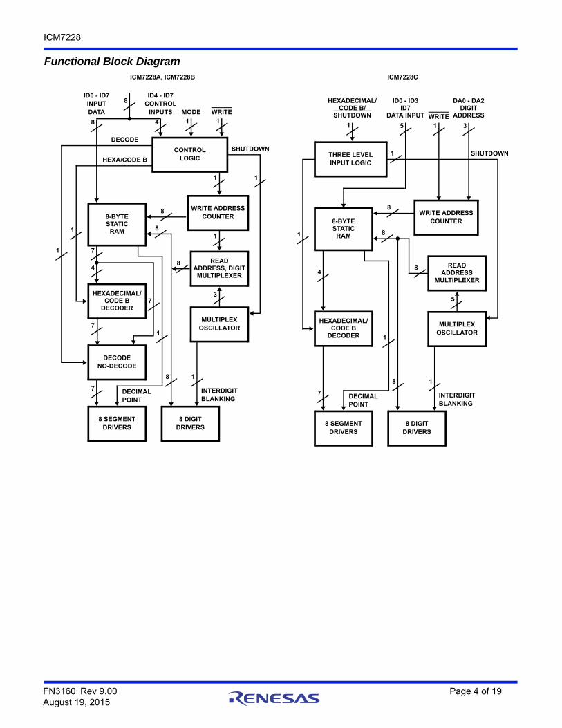
Functional Block Diagram
8 SEGMENTDRIVERS
8 DIGITDRIVERS
DECODENO-DECODE
8-BYTESTATIC
RAM
HEXADECIMAL/CODE B
DECODER
MULTIPLEXOSCILLATOR
WRITE ADDRESSCOUNTER
CONTROLLOGIC
READADDRESS, DIGIT
MULTIPLEXER
ICM7228A, ICM7228B
ID0 - ID7INPUTDATA
ID4 - ID7CONTROL
INPUTS MODE WRITE
SHUTDOWN
HEXA/CODE B
DECODE
INTERDIGITBLANKING
DECIMALPOINT
8
8
4 1 1
1
1
4
7
7
7
8
8
8
1
1
3
18
1
7
1
8 SEGMENTDRIVERS
8 DIGITDRIVERS
8-BYTESTATIC
RAM
HEXADECIMAL/CODE B
DECODER
MULTIPLEXOSCILLATOR
WRITE ADDRESSCOUNTER
THREE LEVELINPUT LOGIC
READADDRESS
MULTIPLEXER
ICM7228C
WRITE
SHUTDOWN
INTERDIGITBLANKING
DECIMALPOINT
1 5 1
1
4
7
8
8
8
5
18
1
1
DA0 - DA2
3
DIGITADDRESS
ID0 - ID3ID7
DATA INPUT
HEXADECIMAL/CODE B/
SHUTDOWN
FN3160 Rev 9.00 Page 4 of 19August 19, 2015
ICM7228
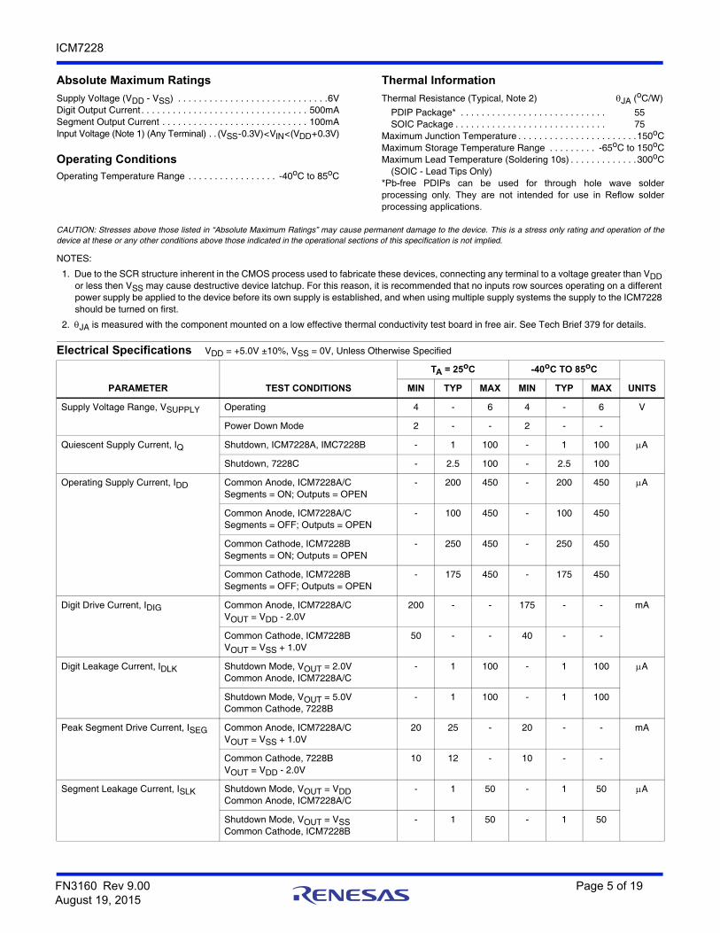
Absolute Maximum Ratings Thermal Information
Supply Voltage (VDD - VSS) . . . . . . . . . . . . . . . . . . . . . . . . . . . . .6VDigit Output Current . . . . . . . . . . . . . . . . . . . . . . . . . . . . . . . . 500mASegment Output Current . . . . . . . . . . . . . . . . . . . . . . . . . . . . 100mAInput Voltage (Note 1) (Any Terminal) . . (VSS-0.3V)<VIN<(VDD+0.3V)
Operating ConditionsOperating Temperature Range . . . . . . . . . . . . . . . . . -40oC to 85oC
Thermal Resistance (Typical, Note 2) JA (oC/W)
PDIP Package* . . . . . . . . . . . . . . . . . . . . . . . . . . . . 55SOIC Package . . . . . . . . . . . . . . . . . . . . . . . . . . . . . 75
Maximum Junction Temperature . . . . . . . . . . . . . . . . . . . . . . .150oCMaximum Storage Temperature Range . . . . . . . . . -65oC to 150oCMaximum Lead Temperature (Soldering 10s) . . . . . . . . . . . . .300oC
(SOIC - Lead Tips Only)*Pb-free PDIPs can be used for through hole wave solderprocessing only. They are not intended for use in Reflow solderprocessing applications.
CAUTION: Stresses above those listed in “Absolute Maximum Ratings” may cause permanent damage to the device. This is a stress only rating and operation of thedevice at these or any other conditions above those indicated in the operational sections of this specification is not implied.
NOTES:
1. Due to the SCR structure inherent in the CMOS process used to fabricate these devices, connecting any terminal to a voltage greater than VDD or less then VSS may cause destructive device latchup. For this reason, it is recommended that no inputs row sources operating on a different power supply be applied to the device before its own supply is established, and when using multiple supply systems the supply to the ICM7228 should be turned on first.
2. JA is measured with the component mounted on a low effective thermal conductivity test board in free air. See Tech Brief 379 for details.
Electrical Specifications VDD = +5.0V ±10%, VSS = 0V, Unless Otherwise Specified
PARAMETER TEST CONDITIONS
TA = 25oC -40oC TO 85oC
UNITSMIN TYP MAX MIN TYP MAX
Supply Voltage Range, VSUPPLY Operating 4 - 6 4 - 6 V
Power Down Mode 2 - - 2 - -
Quiescent Supply Current, IQ Shutdown, ICM7228A, IMC7228B - 1 100 - 1 100 A
Shutdown, 7228C - 2.5 100 - 2.5 100
Operating Supply Current, IDD Common Anode, ICM7228A/CSegments = ON; Outputs = OPEN
- 200 450 - 200 450 A
Common Anode, ICM7228A/CSegments = OFF; Outputs = OPEN
- 100 450 - 100 450
Common Cathode, ICM7228BSegments = ON; Outputs = OPEN
- 250 450 - 250 450
Common Cathode, ICM7228BSegments = OFF; Outputs = OPEN
- 175 450 - 175 450
Digit Drive Current, IDIG Common Anode, ICM7228A/CVOUT = VDD - 2.0V
200 - - 175 - - mA
Common Cathode, ICM7228BVOUT = VSS + 1.0V
50 - - 40 - -
Digit Leakage Current, IDLK Shutdown Mode, VOUT = 2.0VCommon Anode, ICM7228A/C
- 1 100 - 1 100 A
Shutdown Mode, VOUT = 5.0VCommon Cathode, 7228B
- 1 100 - 1 100
Peak Segment Drive Current, ISEG Common Anode, ICM7228A/CVOUT = VSS + 1.0V
20 25 - 20 - - mA
Common Cathode, 7228BVOUT = VDD - 2.0V
10 12 - 10 - -
Segment Leakage Current, ISLK Shutdown Mode, VOUT = VDDCommon Anode, ICM7228A/C
- 1 50 - 1 50 A
Shutdown Mode, VOUT = VSSCommon Cathode, ICM7228B
- 1 50 - 1 50
FN3160 Rev 9.00 Page 5 of 19August 19, 2015

ICM7228
Input Leakage Current, IIL All Inputs Except Pin 9, ICM7228C, VIN = VSS
- - 1 - - 1 A
All Inputs Except Pin 9, ICM7228C, VIN = 5.0V
- - -1 - - -1
Display Scan Rate, fMUX Per Digit - 390 - - 390 - Hz
Inter-Digit Blanking Time, tIDB 2 10 - 2 - - s
Logical “1” Input Voltage, VINH Three Level Input: Pin 9ICM7228C, Hexadecimal VDD = 5V
4.2 - - 4.2 - - V
Floating Input, VINF Three Level Input: Pin 9ICM7228C, Code B, VDD = 5V
2.0 - 3.0 2.0 - 3.0 V
Logical “0” Input Voltage, VINL Three Level Input: Pin 9ICM7228C, Shutdown, VDD = 5V
- - 0.8 - - 0.8 V
Three Level Input Impedance, ZIN VCC = 5V, Pin 9 of ICM7228C 50 - - 50 - - k
Logical “1” Input Voltage, VIH All Inputs Except, Pin 9 of ICM7228C, VDD = 5V
2.0 - - 2.0 - - V
Logical “0” Input Voltage, VIL All Inputs Except, Pin 9 of ICM7228C, VDD = 5V
- - 0.8 - - 0.8 V
SWITCHING SPECIFICATIONS VDD = +5.0V 10%, VSS = 0V, VIL = +0.4V, VIH = +2.4V
Write Pulsewidth (Low), tWL 200 100 - 250 - - ns
Write Pulsewidth (High), tWH 850 540 - 1200 - - ns
Mode Hold Time, tMH ICM7228A, ICM7228B 0 -65 - 0 - - ns
Mode Setup Time, tMS ICM7228A, ICM7228B 250 150 - 250 - - ns
Data Setup Time, tDS 250 160 - 250 - - ns
Data Hold Time, tDH 0 -60 - 0 - - ns
Digit Address Setup Time, tAS ICM7228C 250 110 - 250 - - ns
Digit Address Hold Time, tAH ICM7228C 0 -60 - 0 - - ns
Electrical Specifications VDD = +5.0V ±10%, VSS = 0V, Unless Otherwise Specified (Continued)
PARAMETER TEST CONDITIONS
TA = 25oC -40oC TO 85oC
UNITSMIN TYP MAX MIN TYP MAX
FN3160 Rev 9.00 Page 6 of 19August 19, 2015
ICM7228
Timing Diagrams
FIGURE 1. ICM7228A/B WRITE CYCLE FIGURE 2. ICM7228A/B SEQUENTIAL 8-DIGIT RAM UPDATE
FIGURE 3. ICM7228C WRITE CYCLE
FIGURE 4. DISPLAY DIGITS MULTIPLEX (COMMON ANODE DISPLAY)
tMS
tWL
tDS
tMH
MODE
INPUTVALIDDATA
tDH
tWH
WRITE
DECODE/NO DECODE? ID5
(D8)(D1)
MODE
CONTROL WORDTYPE OF DECODER?ID6DECODE/NO DECODE? ID5SHUTDOWN?ID4DATA COMING ID7
CONTROL WORDTYPE OF DECODER?ID6
SHUTDOWN? ID4DATA COMING ID7
DON’T CAREWRITE DATA8 PULSES
WRITE
VALID DATA
VALID
tWL tWH
tAS tAH
tDHtDS
DATA
WRITE
DIGITADDRESSDAO-DAZ
INTERDIGIT BLANKINGINTERNAL SIGNAL
TYPICAL DIGITSOUTPUT PULSES
10s (TYP)FREE RUNNING
320s (TYP)FREE RUNNING (PER DIGIT)
INTERDIGIT BLANKING
D2
D5
D1
D7
D8
D6
D4
D3
FN3160 Rev 9.00 Page 7 of 19August 19, 2015
ICM7228
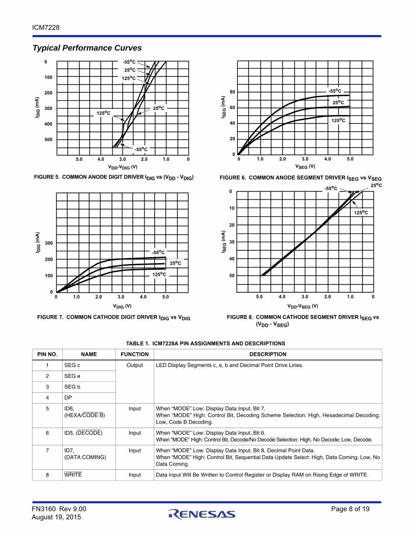
Typical Performance Curves
FIGURE 5. COMMON ANODE DIGIT DRIVER IDIG vs (VDD - VDIG) FIGURE 6. COMMON ANODE SEGMENT DRIVER ISEG vs VSEG
FIGURE 7. COMMON CATHODE DIGIT DRIVER IDIG vs VDIG FIGURE 8. COMMON CATHODE SEGMENT DRIVER ISEG vs (VDD - VSEG)
TABLE 1. ICM7228A PIN ASSIGNMENTS AND DESCRIPTIONS
PIN NO. NAME FUNCTION DESCRIPTION
1 SEG c Output LED Display Segments c, e, b and Decimal Point Drive Lines.
2 SEG e
3 SEG b
4 DP
5 ID6,(HEXA/CODE B)
Input When “MODE” Low: Display Data Input, Bit 7.When “MODE” High: Control Bit, Decoding Scheme Selection: High, Hexadecimal Decoding;Low, Code B Decoding.
6 ID5, (DECODE) Input When “MODE” Low: Display Data Input, Bit 6.When “MODE” High: Control Bit, Decode/No Decode Selection: High, No Decode; Low, Decode.
7 ID7,(DATA COMING)
Input When “MODE” Low: Display Data Input, Bit 8, Decimal Point Data.When “MODE” High: Control Bit, Sequential Data Update Select: High, Data Coming; Low, NoData Coming.
8 WRITE Input Data Input Will Be Written to Control Register or Display RAM on Rising Edge of WRITE.
VDD-VDIG (V)
I DIG
(m
A)
0
100
200
300
400
500
01.02.03.04.05.0
-55oC
25oC
125oC
-55oC
25oC125oC
VSEG (V)
I SE
G (
mA
)
80
60
40
20
00 1.0 2.0 3.0 4.0 5.0
-55oC
25oC
125oC
VDIG (V)
I DIG
(m
A)
300
200
100
00 1.0 2.0 3.0 4.0 5.0
-55oC
25oC
125oC
VDD-VSEG (V)
0
10
20
30
40
50
01.02.03.04.05.0
I SE
G (
mA
)
-55oC25oC
125oC
FN3160 Rev 9.00 Page 8 of 19August 19, 2015
ICM7228
9 MODE Input Selects Data to Be Loaded to Control Register or Display RAM: High, Loads Control Register;Low, Loads Display RAM.
10 ID4,(SHUTDOWN)
Input When “MODE” Low: Display Data Input, Bit 5.When “MODE” High: Control Bit, Low Power Mode Select: High, Normal Operation; Low,Oscillator and Display Disabled.
11 ID1 Input When “MODE” Low: Display Data Input, Bit 2.When “MODE” High and “ID7 (DATA COMING)” Low: Digit Address, Bit 2, Single Digit UpdateMode.
12 ID0 Input When “MODE” Low: Display Data Input, Bit 1.When “MODE” High and “ID7 (DATA COMING)” Low: Digit Address, LSB, Single Digit UpdateMode.
13 ID2 Input When “MODE” Low: Display Data Input, Bit 3.When “MODE” High and “ID7 (DATA COMING)” Low: Digit Address, MSB, Single Digit UpdateMode.
14 ID3 Input When “MODE” Low: Display Data Input, Bit 4.When “MODE” High: RAM Bank Select (Decode Modes Only): High, RAM Bank A; Low, RAMBank B
15 DIGIT 1 Output LED Display Digits 1, 2, 5 and 8 Drive Lines.
16 DlGlT 2
17 DIGIT 5
18 DlGlT 8
19 VDD Supply Device Positive Power Supply Rail.
20 DIGIT 4 Output LED Display Digits 4, 7, 6 and 3 Drive Lines.
21 DlGlT 7
22 DlGlT 6
23 DIGlT 3
24 SEG f Output LED Display Segments f, d, g and a Drive Lines.
25 SEG d
26 SEG g
27 SEG a
28 VSS Supply Device Ground or Negative Power Supply Rail.
TABLE 2. ICM7228B PIN ASSIGNMENTS AND DESCRIPTIONS
PIN NO. NAME FUNCTION DESCRIPTION
1 DIGIT 4 Output LED Display Digits 4, 6, 3 and 1 Drive Lines.
2 DlGlT 6
3 DIGIT 3
4 DlGlT 1
5 ID6,(HEXA/CODE B)
Input When “MODE” Low: Display Data Input, Bit 7.When “MODE” High: Control Bit, Decoding Scheme Selection: High, Hexadecimal Decoding; Low, Code B Decoding.
6 ID5, (DECODE) Input When “MODE” Low: Display Data Input, Bit 6.When “MODE” High: Control Bit, Decode/No Decode Selection: High, No Decode; Low, Decode.
7 ID7,(DATA COMING)
Input When “MODE” Low: Display Data Input, Bit 8, Decimal Point Data.When “MODE” High: Control Bit, Sequential Data Update Select: High, Data Coming; Low, NoData Coming.
TABLE 1. ICM7228A PIN ASSIGNMENTS AND DESCRIPTIONS (Continued)
PIN NO. NAME FUNCTION DESCRIPTION
FN3160 Rev 9.00 Page 9 of 19August 19, 2015
ICM7228
8 WRITE Input Data Input Will Be Written to Control Register or Display RAM on Rising Edge of WRITE.
9 MODE Input Selects Data to Be Loaded to Control Register or Display RAM: High, Loads Control Register;Low, Loads Display RAM.
10 ID4,(SHUTDOWN)
Input When “MODE” Low: Display Data Input, Bit 5.When “MODE” High: Control Bit, Low Power Mode Select: High, Normal Operation; Low,Oscillator and Display Disabled.
11 ID1 Input When “MODE” Low: Display Data Input, Bit 2.When “MODE” High and “ID7 (DATA COMING)” Low: Digit Address, Bit 2, Single Digit UpdateMode.
12 ID0 Input When “MODE” Low: Display Data Input, Bit 1.When “MODE” High and “ID7 (DATA COMING)” Low: Digit Address, LSB, Single Digit UpdateMode.
13 ID2 Input When “MODE” Low: Display Data Input, Bit 3.When “MODE” High and “ID7 (DATA COMING)” Low: Digit Address, MSB, Single Digit UpdateMode.
14 ID3 Input When “MODE” Low: Display Data Input, Bit 4.When “MODE” High: RAM Bank Select (Decode Modes Only): High, RAM Bank A; Low, RAMBank B.
15 DP Output LED Display Decimal Point and Segments a, b, and d Drive Lines
16 SEG a
17 SEG b
18 SEG d
19 VDD Supply Device Positive Power Supply Rail.
20 SEG c Output LED Display Segments c, e, f and g Drive Lines.
21 SEG e
22 SEG f
23 SEG g
24 DIGIT 8 Output LED Display Digits 8, 2, 5 and 7 Drive Lines.
25 DIGIT 2
26 DIGIT 5
27 DIGIT 7
28 VSS Supply Device Ground or Negative Power Supply Rail.
TABLE 3. ICM7228C PIN ASSIGNMENTS AND DESCRIPTIONS
PIN NO. NAME FUNCTION DESCRIPTION
1 SEG c Output LED Display Segments c, e, band Decimal Point Drive Lines.
2 SEG e
3 SEG b
4 DP
5 DA0 Input Digit Address Input, Bit 1 LSB.
6 DA1 Input Digit Address Input, Bit 2.
7 ID7,(INPUT DP)
Input Display Decimal Point Data Input, Negative True.
8 WRITE Input Data Input Will Be Written to Display RAM on Rising Edge of WRITE.
TABLE 2. ICM7228B PIN ASSIGNMENTS AND DESCRIPTIONS (Continued)
PIN NO. NAME FUNCTION DESCRIPTION
FN3160 Rev 9.00 Page 10 of 19August 19, 2015
ICM7228
Detailed DescriptionSystem Interfacing and Data Entry Modes, ICM7228A and ICM7228B
The ICM7228A/B devices are compatible with the architectures of most microprocessor systems. Their fast switching characteristics makes it possible to access them as a memory mapped I/O device with no wait state necessary in most microcontroller systems. All the ICM7228A/B inputs, including MODE, feature a 250ns minimum setup and 0ns hold time with a 200ns minimum WRITE pulse. Input logic levels are TTL and CMOS compatible. Figure 9 shows a generic method of driving the ICM7228A/B from a microprocessor bus. To the microprocessor, each device appears to be 2 separate I/O locations; the Control Register and the Display RAM. Selection between the two is accomplished by the MODE input driven by address line A0. Input data is placed on the lD0 - lD7 lines. The WRITE input acts as both a device select and write cycle timing pulse. See Figure 1 and Switching Specifications Table for write cycle timing parameters.
The ICM7228A/B have three data entry modes: Control Register update without RAM update, sequential 8-digit update and single digit update. In all three modes a control word is first written by pulsing the WRITE input while the MODE input is high, thereby latching data into the Control Register. The logic
level of individual bits in the Control Register select Shutdown, Decode/No Decode, Hex/Code B, RAM bank A/B and Display RAM digit address as shown in Tables 1 and 2.
The ICM7228A/B Display RAM is divided into 2 banks, called bank A and B. When using the Hexadecimal or code B display modes, these RAM banks can be selected separately. This allows two separate sets of display data to be stored and displayed alternately. Notice that the RAM bank selection is not possible in No-Decode mode, this is because the display data in the No-Decode mode has 8 bits, but in Decoded schemes (Hex/Code B) is only 4 bits (lD0 - lD3 data). It should also be mentioned that the decimal point is independent of selected bank, a turned on decimal point will remain on for either bank. Selection of the RAM banks is controlled by lD3 input. The lD3 logic level (during Control Register update) selects which bank of the internal RAM to be written to and/or displayed.
Control Register Update without RAM Update
The Control Register can be updated without changing the display data by a single pulse on the WRITE input, with MODE high and DATA COMING low. If the display is being decoded (Hex/Code B), then the value of lD3 determines which RAM bank will be selected and displayed for all eight digits.
Sequential 8-Digit Update
9 HEXA/CODE B/SHUTDOWN
Input Three Level Input. Display Function Control: High, Hexadecimal Decoding; Float, Code BDecoding; Low, Oscillator, and Display Disabled.
10 DA2 Input Digit Address Input, Bit 3, MSB.
11 ID1 Input Display Data Inputs.
12 ID0
13 ID2
14 ID3
15 DIGIT 1 Output LED Display Digits 1, 2, 5 and 8 Drive Lines.
16 DlGlT 2
17 DIGIT 5
18 DlGlT 8
19 VDD Supply Device Positive Power Supply Rail.
20 DIGIT 4 Output LED Display Digits 4, 7, 6 and 3 Drive Lines.
21 DlGlT 7
22 DlGlT 6
23 DIGlT 3
24 SEG f Output LED Display Segments f, d, g and a Drive Lines.
25 SEG d
26 SEG g
27 SEG a
28 VSS Supply Device Ground or Negative Power Supply Rail.
TABLE 3. ICM7228C PIN ASSIGNMENTS AND DESCRIPTIONS (Continued)
PIN NO. NAME FUNCTION DESCRIPTION
FN3160 Rev 9.00 Page 11 of 19August 19, 2015

ICM7228
The logic state of DATA COMING (lD7) is also latched during a Control Register update. If the latched value of DATA COMING (lD7) is high, the display becomes blanked and a sequential 8-digit update is initiated. Display data can now be written into RAM with 8 successive WRITE pulses, starting with digit 1 and ending with digit 8 (See Figure 2). After all 8 RAM locations have been written to, the display turns on again and the new data is displayed. Additional write pulses are ignored until a new Control Register update is performed. All 8 digits are displayed in the format (Hex/Code B or No Decode) specified by the control word that preceded the 8 digit update. If a decoding scheme (Hex/Code B) is to be used, the value of lD3 during the control word update determines which RAM bank will be written to.
Single Digit Update
In this mode each digit data in the display RAM can be updated individually without changing the other display data. First, with MODE input high, a control word is written to the Control Register carrying the following information; DATA COMING (lD7) low, the desired display format data on lD4 - lD6, the RAM bank selected by lD3 (if decoding is selected) and the address of the digit to be updated on data lines lD0 - lD2 (See Table 4). A second write to the ICM7228A/B, this time with MODE input low, transfers the data at the lD0 - lD7 inputs into the selected digit’s RAM location. In single digit update mode, each individual digit’s data can be specified independently for being displayed in Decoded or No-Decode mode. For those digits which decoding scheme (Hex/Code B) is selected, only one can be effective at a time. Whenever a control word is written, the specified decoding scheme will be applied to all those digits which selected to be displayed in Decoded mode.
System Interfacing, ICM7228C
The ICM7228C is directly compatible with the architecture of most microprocessor systems. Its fast switching characteristics make it possible to access them as a memory mapped I/O device with no wait state necessary in most microcontroller systems. All the ICM7228C inputs, excluding HEXA/CODE B/SHUTDOWN, feature a 250ns minimum setup and 0ns hold time with a 200ns minimum WRITE pulse. Input logic levels are
TTL and CMOS compatible. Figure 10 shows a generic method of driving the ICM7228C from a microprocessor bus. To the microprocessor, the 8 bytes of the Display RAM appear to be 8 separate I/O locations. Loading the ICM7228C is quite similar to a standard memory write cycle. The address of the digit to be updated is placed on lines DA0 - DA2, the data to be written is placed on lines ID0 - lD3 and ID7, then a low pulse on WRITE input will transfer the data in. See Figure 3 and Switching Characteristics Table for write cycle timing parameters.
The ICM7228C does not have any control register, and also does not provide the No Decode display format. Hexadecimal or Code B character selection and shutdown mode are directly controlled through the three level input at Pin 9, which is accordingly called HEXA/CODE B/SHUTDOWN. See Table 3 for input and output definitions of the ICM7228C.
Display Formats
The ICM7228A and ICM7228B have three possible display formats; Hexadecimal, Code B and No Decode. Table 5 shows the character sets for the decode modes and their corresponding input code.
I/O ORMEMORYWRITE PULSE DECODER
ENABLE
ADDRESSDECODER
ID0
ID7 INTERSILICM7228A/B
SEGMENTSDRIVE
WRITE
MODE
DIGITSDRIVE
A0
DEVICE SELECTAND
WRITE PULSE
LED DISPLAY
ADDRESS BUS A0 - A15
A1-A15
DATA BUS D0-D7
D0 - D7
MIC
RO
PR
OC
ES
SO
R S
YS
TE
M
FIGURE 9. ICM7228A/B MICROPROCESSOR SYSTEM INTERFACING
TABLE 4. DIGITS ADDRESS, ICM7228A/B
INPUT DATA LINES
SELECTED DIGIT1D2 lD2 lD0
0 0 0 DlGlT 1
0 0 1 DlGlT 2
0 1 0 DIGlT 3
0 1 1 DlGlT 4
1 0 0 DIGIT 5
1 0 1 DlGlT 6
1 1 0 DlGlT 7
1 1 1 DlGlT 8
FN3160 Rev 9.00 Page 12 of 19August 19, 2015

ICM7228
The display formats of the ICM7228A/B are selected by writing data to bits ID4, ID5 and ID6 of the Control Register (See Table 1 and 2 for input Definitions). Hexadecimal and Code B data is entered via ID0-lD3 and ID7 controls the decimal point.
The No Decode mode of the ICM7228A and ICM7228B allows the direct segment-by-segment control of all 64 segments driven by the device. In the No Decode mode, the input data directly control the outputs as shown in Table 6.
An input high level turns on the respective segment, except for the decimal point, which is turned on by an input low level on ID7.
The No Decode mode can be used in different applications such as bar graph or status panel driving where each segment controls an individual LED.
The ICM7228C has only the Hexadecimal and Code B character sets. The HEXA/CODE B/SHUTDOWN input, pin 9, requires a three level input. Pin 9 selects the Hexadecimal format when pulled high, the Code B format when floating or driven to mid-supply, and the shutdown mode when pulled low (See Table 3). Table 5 also applies to the ICM7228C.
Shutdown and Display Banking
When shutdown, the ICM7228 enters a low power standby mode typically consuming only 1A of supply current for the ICM7228A/B and 2.5A for the ICM7228C. In this mode the ICM7228 turns off the multiplex scan oscillator as well as the digit and segment drivers. However, input data can still be entered when in the shutdown mode. Data is retained in memory even with the supply voltage as low as 2V.
The ICM7228A/B is shutdown by writing a control word with Shutdown (lD4) low. The ICM7228C is put into shutdown mode by driving pin 9, HEXA/CODE B/SHUTDOWN, low.
TABLE 5. DISPLAY CHARACTER SETS
INPUT DATA CODE DISPLAY CHARACTERS
ID3 ID2 ID1 ID0 HEXADECIMAL CODE B
0 0 0 0 0 0
0 0 0 1 1 1
0 0 1 0 2 2
0 0 1 1 3 3
0 1 0 0 4 4
0 1 0 1 5 5
0 1 1 0 6 6
0 1 1 1 7 7
1 0 0 0 8 8
1 0 0 1 9 9
1 0 1 0 A -
1 0 1 1 b E
1 1 0 0 C H
1 1 0 1 d L
1 1 1 0 E P
1 1 1 1 F (Blank)
TABLE 5. DISPLAY CHARACTER SETS (Continued)
INPUT DATA CODE DISPLAY CHARACTERS
ID3 ID2 ID1 ID0 HEXADECIMAL CODE B
I/O ORMEMORYWRITE PULSE DECODER
ENABLE
ADDRESSDECODER
ID0 - ID3
INTERSILICM7228C
SEGMENTSDRIVE
WRITE
DA0 - DA2 DIGITSDRIVE
A0 - A2
DEVICE SELECTAND
WRITE PULSE
LED DISPLAY
ADDRESS BUS A0 - A15
A3 - A15
DATA BUS D0 - D7
MIC
RO
PR
OC
ES
SO
R S
YS
TE
M
AND ID7
5
FIGURE 10. ICM7228C MICROPROCESSOR SYSTEM INTERFACING
TABLE 6. NO DECODE SEGMENT LOCATIONS
DATAINPUT ID7 ID6 ID5 ID4 ID3 ID2 ID1 ID0
ControlledSegment
Decimal Point
a b c e g f d
ab
cd
fg
e
DP
FIGURE 11. DIGITS SEGMENT ASSIGNMENTS
FN3160 Rev 9.00 Page 13 of 19August 19, 2015
ICM7228
The ICM7228 operating current with the display blanked is within 100A - 200A for all versions. All versions of the ICM7228 can be blanked by writing Hex FF to all digits and selecting Code B format. The ICM7228A and ICM7228B can also be blanked by selecting No Decode mode and writing Hex 80 to all digits (See Tables 5and 6).
Common Anode Display Drivers, ICM7228A and ICM7228C
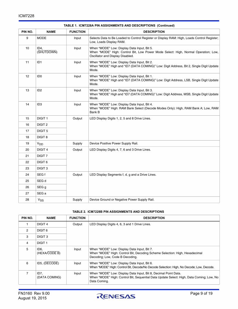
The common anode digit and segment driver output schematics are shown in Figure 12. The common anode digit driver output impedance is approximately 4. This provides a nearly constant voltage to the display digits. Each digit has a minimum of 200mA drive capability. The N-Channel segment driver’s output impedance of 50 limits the segment current to approximately 25mA peak current per segment. Both the segment and digit outputs can directly drive the display, current limiting resistors are not required.
Individual segment current is not significantly affected by whether other segments are on or off. This is because the segment driver output impedance is much higher than that of the digit driver. This feature is important in bar graph applications where each bar graph element should have the same brightness, independent of the number of elements being turned on.
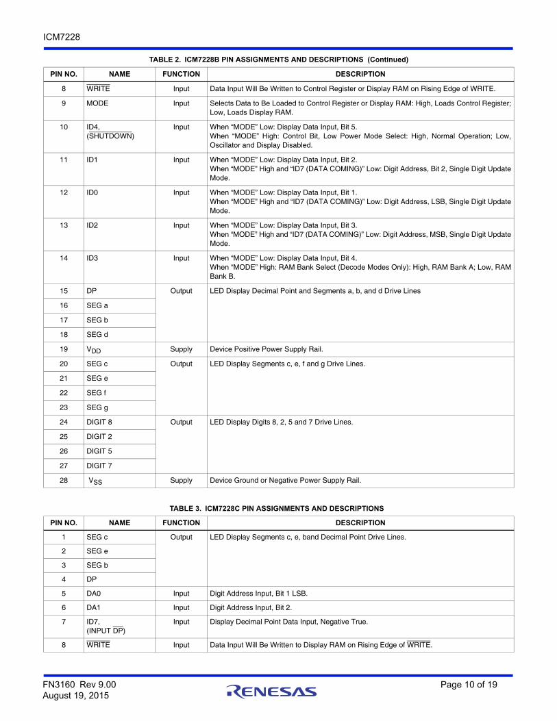
Common Cathode Display Driver, ICM7228B
The common cathode digit and segment driver output schematics are shown in Figure 13. The N-channel digit drivers have an output impedance of approximately 15. Each digit has a minimum of 50mA drive capability. The segment drivers have an output impedance of approximately 100 with typically 10mA peak current drive for each segment. The common cathode display driver output currents are only 1/4 of the common anode display driver currents. Therefore, the ICM7228A and ICM7228C common anode display drivers are recommended for those applications where high display brightness is desired. The ICM7228B common cathode display driver is suitable for driving bubble-lensed monolithic 7 segment displays. They can also drive individual LED displays up to 0.3 inches in height when high brightness is not required.
Display Multiplexing
Each digit of the ICM7228 is on for approximately 320s, with a multiplexing frequency of approximately 390Hz. The ICM7228 display drivers provide interdigit blanking. This ensures that the segment information of the previous digit is gone and the information of the next digit is stable before the next digit is driven on. This is necessary to eliminate display ghosting (a faint display of data from previous digit superimposed on the next digit). The interdigit blanking time is 10s typical with a guaranteed 2s minimum. The ICM7228 turns off both the digit drivers and the segment drivers during the interdigit blanking period. The digit multiplexing sequence is: D2, D5, D1, D7, D8, D6, D4 and D3. A typical digit’s drive pulses are shown on Figure 4.
Due to the display multiplexing, the driving duty cycle for each digit is 12% (100 x 1/8) This means the average current for each segment is 1/8 of its peak current. This must be considered while designing and selecting the displays.
Driving Larger Displays
If very high display brightness is desired, the ICM7228 display driver outputs can be externally buffered. Figures 14 thru 16 show how to drive either common anode or common cathode displays using the ICM7228 and external driver circuit for higher current displays.
Another method of increasing display currents is to connect two digit outputs together and load the same data into both digits. This drives the display with the same peak current, but the average current doubles because each digit of the display is on for twice as long, i.e., 1/4 duty cycle versus 1/8.
DIGITSTROBE
INTERDIGITBLANKING
SHUTDOWN
VDD
200mA
COMMONANODEDIGITOUTPUT2k
N
VSS
P
2k
N
VSS
N
N
NOTE: When SHUTDOWN goes low INTERDIGIT BLANKING also stays low.
FIGURE 12A. DIGIT DRIVER
SEGMENTDATA
INTERDIGITBLANKING
SHUTDOWN
VDD
COMMONANODESEGMENTOUTPUT
2k
VSS
N
P
75
FIGURE 12B. SEGMENT DRIVER
FIGURE 12. COMMON ANODE DISPLAY DRIVERS
FN3160 Rev 9.00 Page 14 of 19August 19, 2015

ICM7228
DIGITSTROBE
INTERDIGITBLANKING
SHUTDOWN
VDD
COMMONCATHODEDIGITOUTPUT
2k
VSS
N
P
15
FIGURE 13A. DIGIT DRIVER
SEGMENTDATA
INTERDIGITBLANKING
SHUTDOWN
VDD
200mA
COMMONCATHODESEGMENTOUTPUT
2kN
VSS
P
2k
N
VSS
N
100
NOTE: When SHUTDOWN goes low INTERDIGIT BLANKING also stays low.
FIGURE 13B. SEGMENT DRIVER
FIGURE 13. COMMON CATHODE DISPLAY DRIVERS
VDD
ICM7228A/C
SEGMENTOUTPUT
DIGITOUTPUT
VSS
UP TO
10K
VDD
VSS
VDD
VDD
4A
FIGURE 14. DRIVING HIGH CURRENT DISPLAY, COMMON ANODE ICM7228A/C TO COMMON ANODE
VDD
ICM7228B
100SEGMENT
OUTPUT
DIGITOUTPUT
N
VSS
15
2N6034
14(100mAPEAK)
2N2219
VSS
VDD
1.4APEAK
14mA
VDD
FIGURE 15. DRIVING HIGH CURRENT DISPLAY, COMMON CATHODE ICM7228B TO COMMON CATHODE DISPLAY
VDD
ICM7228B
100SEGMENT
OUTPUT
300DIGIT
OUTPUT
N
VSS
15 1K
2N2219
(100mAPEAK)
25
2N6034
1.4APEAK
1K
VDD
VSS
1K
VDD
VDD
FIGURE 16. DRIVING HIGH CURRENT DISPLAY, COMMON CATHODE ICM7228B TO COMMON ANODE DISPLAY
FN3160 Rev 9.00 Page 15 of 19August 19, 2015

ICM7228
Three Level Input, ICM7228C
As mentioned before, pin 9 is a three level input and controls three functions: Hexadecimal display decoding, Code B display decoding and shutdown mode. In many applications, pin 9 will be left open or permanently wired to one state. When pin 9 can not be permanently left in one state, the circuits illustrated in Figure 17 can be used to drive this three level input.
Power Supply Bypassing
Connect a minimum of 47F in parallel with 0.1F capacitors between VDD and VSS of ICM7228. These capacitors should be placed in close proximity to the device to reduce the power supply ripple caused by the multiplexed LED display drive current pulses.
HIGH = HEX
LOW = SHUTDOWN
HIGH = HEX OR SHUTDOWN
LOW = CODE B
HIGH = HEX
LOW = SHUTDOWN
HIGH = HEX OR SHUTDOWN
LOW = CODE B
HIGH = CODE B
LOW = HEX
HIGH = SHUTDOWN
LOW = CODE B
HIGH = SHUTDOWN
LOW = HEX
HIGH = SHUTDOWN
LOW = CODE B
PIN 9
PIN 9
PIN 9
PIN 9
PIN 9
PIN 9
CD4016CD4066
CONTROL
CD4069
CD4069
CD4069
1N4148
1N4148
OPEN DRAIN OR OPEN COLLECTOR OUTPUT
74C126 THREE-STATE BUFFER
FIGURE 17. ICM7228C PIN 9 DRIVE CIRCUITS
Test Circuit
FIGURE 18. FUNCTIONAL TEST CIRCUIT #1
ID6 (HEXA/CODE B)
ID5 (DECODE)
ID7 (DATA COMING)
WRITE
MODE
ID4 (SHUTDOWN)
ID1
ID0
ID2
ID3
28
27
26
25
24
23
22
21
20
19
18
17
16
15
1
2
3
4
5
6
7
8
9
10
11
12
13
14
D8 D7 D6 D5 D4 D3 D2 D1
f
d
g
a
c
e
b
DPCOMMON ANODE DISPLAY
VDD
47F+0.1F
VSS
5V
+
-
VDD
VSS
ICM7228A
FN3160 Rev 9.00 Page 16 of 19August 19, 2015
ICM7228
About IntersilIntersil Corporation is a leading provider of innovative power management and precision analog solutions. The company's products address some of the largest markets within the industrial and infrastructure, mobile computing and high-end consumer markets.
For the most updated datasheet, application notes, related documentation and related parts, please see the respective product information page found at www.intersil.com.
You may report errors or suggestions for improving this datasheet by visiting www.intersil.com/ask.
Reliability reports are also available from our website at www.intersil.com/support
Revision HistoryThe revision history provided is for informational purposes only and is believed to be accurate, but not warranted. Please go to the web to make sure that you have the latest revision.
DATE REVISION CHANGE
August 19, 2015 FN3160.9 Updated Ordering Information table and moved it from page 1 to page 2.Added Revision History and About Intersil sections.Updated POD M28.3 to current revision. Changes: Added land pattern
FN3160 Rev 9.00 Page 17 of 19August 19, 2015

ICM7228
FN3160 Rev 9.00 Page 18 of 19August 19, 2015
Dual-In-Line Plastic Packages (PDIP)
NOTES:
1. Controlling Dimensions: INCH. In case of conflict between English and Metric dimensions, the inch dimensions control.
2. Dimensioning and tolerancing per ANSI Y14.5M-1982.
3. Symbols are defined in the “MO Series Symbol List” in Section 2.2 of Publication No. 95.
4. Dimensions A, A1 and L are measured with the package seated in JEDEC seating plane gauge GS-3.
5. D, D1, and E1 dimensions do not include mold flash or protrusions. Mold flash or protrusions shall not exceed 0.010 inch (0.25mm).
6. E and are measured with the leads constrained to be perpendic-ular to datum .
7. eB and eC are measured at the lead tips with the leads unconstrained. eC must be zero or greater.
8. B1 maximum dimensions do not include dambar protrusions. Dambar protrusions shall not exceed 0.010 inch (0.25mm).
9. N is the maximum number of terminal positions.
10. Corner leads (1, N, N/2 and N/2 + 1) for E8.3, E16.3, E18.3, E28.3, E42.6 will have a B1 dimension of 0.030 - 0.045 inch (0.76 - 1.14mm).
eA-C-
CL
E
eA
C
eB
eC
-B-
E1INDEX
1 2 3 N/2
N
AREA
SEATING
BASEPLANE
PLANE
-C-
D1
B1B
e
D
D1
AA2
L
A1
-A-
0.010 (0.25) C AM B S
E28.6 (JEDEC MS-011-AB ISSUE B)28 LEAD DUAL-IN-LINE PLASTIC PACKAGE
SYMBOL
INCHES MILLIMETERS
NOTESMIN MAX MIN MAX
A - 0.250 - 6.35 4
A1 0.015 - 0.39 - 4
A2 0.125 0.195 3.18 4.95 -
B 0.014 0.022 0.356 0.558 -
B1 0.030 0.070 0.77 1.77 8
C 0.008 0.015 0.204 0.381 -
D 1.380 1.565 35.1 39.7 5
D1 0.005 - 0.13 - 5
E 0.600 0.625 15.24 15.87 6
E1 0.485 0.580 12.32 14.73 5
e 0.100 BSC 2.54 BSC -
eA 0.600 BSC 15.24 BSC 6
eB - 0.700 - 17.78 7
L 0.115 0.200 2.93 5.08 4
N 28 28 9
Rev. 1 12/00
FN3160 Rev 9.00 Page 19 of 19August 19, 2015
ICM7228
Intersil products are manufactured, assembled and tested utilizing ISO9001 quality systems as notedin the quality certifications found at www.intersil.com/en/support/qualandreliability.html
Intersil products are sold by description only. Intersil may modify the circuit design and/or specifications of products at any time without notice, provided that such modification does not, in Intersil's sole judgment, affect the form, fit or function of the product. Accordingly, the reader is cautioned to verify that datasheets are current before placing orders. Information furnished by Intersil is believed to be accurate and reliable. However, no responsibility is assumed by Intersil or its subsidiaries for its use; nor for any infringements of patents or other rights of third parties which may result from its use. No license is granted by implication or otherwise under any patent or patent rights of Intersil or its subsidiaries.
For information regarding Intersil Corporation and its products, see www.intersil.com
For additional products, see www.intersil.com/en/products.html
© Copyright Intersil Americas LLC 2002-2015. All Rights Reserved.All trademarks and registered trademarks are the property of their respective owners.
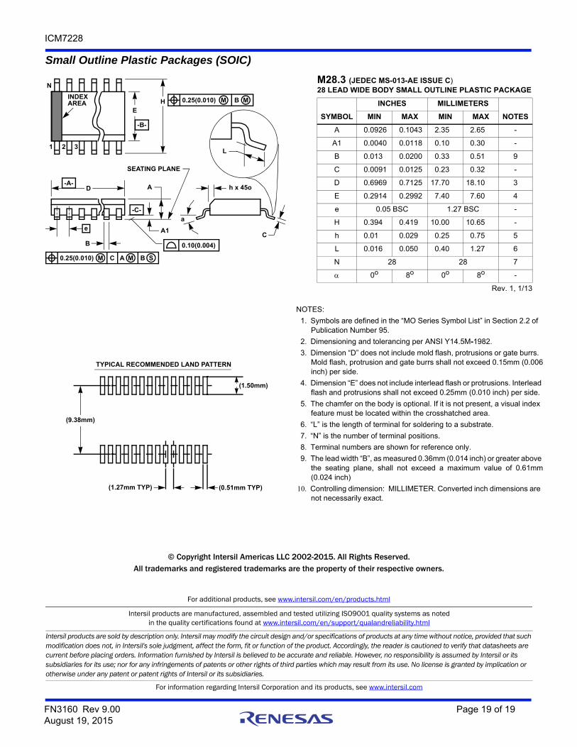
Small Outline Plastic Packages (SOIC)
a
INDEXAREA
E
D
N
1 2 3
-B-
0.25(0.010) C AM B S
e
-A-
L
B
M
-C-
A1
A
SEATING PLANE
0.10(0.004)
h x 45o
C
H 0.25(0.010) BM M
(1.50mm)
(9.38mm)
(1.27mm TYP) (0.51mm TYP)
TYPICAL RECOMMENDED LAND PATTERN
M28.3 (JEDEC MS-013-AE ISSUE C)28 LEAD WIDE BODY SMALL OUTLINE PLASTIC PACKAGE
SYMBOL
INCHES MILLIMETERS
NOTESMIN MAX MIN MAX
A 0.0926 0.1043 2.35 2.65 -
A1 0.0040 0.0118 0.10 0.30 -
B 0.013 0.0200 0.33 0.51 9
C 0.0091 0.0125 0.23 0.32 -
D 0.6969 0.7125 17.70 18.10 3
E 0.2914 0.2992 7.40 7.60 4
e 0.05 BSC 1.27 BSC -
H 0.394 0.419 10.00 10.65 -
h 0.01 0.029 0.25 0.75 5
L 0.016 0.050 0.40 1.27 6
N 28 28 7
0o 8o 0o 8o -
Rev. 1, 1/13
NOTES:
1. Symbols are defined in the “MO Series Symbol List” in Section 2.2 of Publication Number 95.
2. Dimensioning and tolerancing per ANSI Y14.5M-1982.
3. Dimension “D” does not include mold flash, protrusions or gate burrs. Mold flash, protrusion and gate burrs shall not exceed 0.15mm (0.006inch) per side.
4. Dimension “E” does not include interlead flash or protrusions. Interlead flash and protrusions shall not exceed 0.25mm (0.010 inch) per side.
5. The chamfer on the body is optional. If it is not present, a visual index feature must be located within the crosshatched area.
6. “L” is the length of terminal for soldering to a substrate.
7. “N” is the number of terminal positions.
8. Terminal numbers are shown for reference only.
9. The lead width “B”, as measured 0.36mm (0.014 inch) or greater above the seating plane, shall not exceed a maximum value of 0.61mm(0.024 inch)
10. Controlling dimension: MILLIMETER. Converted inch dimensions are not necessarily exact.
Recommended