8/6/2019 Design and Analog VLSI Implementation of Artificial Neural Network
http://slidepdf.com/reader/full/design-and-analog-vlsi-implementation-of-artificial-neural-network 1/14
International Journal of Artificial Intelligence & Applications (IJAIA), Vol.2, No.3, July 2011
DOI : 10.5121/ijaia.2011.2309 96
DESIGN AND ANALOG VLSI
IMPLEMENTATION OF ARTIFICIAL
NEURAL NETWORK
Prof. Bapuray.D.Yammenavar1, Vadiraj.R.Gurunaik
2,
Rakesh.N.Bevinagidad3and Vinayak.U.Gandage
4
1,2,3,4Dept of Electronics & Communication, BLDEA’s College of Engg & Tech,
Bijapur, Visvesvaraya Technological University, Karnataka, India.
[email protected], [email protected]
3
A BSTRACT
Nature has evolved highly advanced systems capable of performing complex computations, adoption and learning using analog computations. Furthermore nature has evolved techniques to deal with imprecise
analog computations by using redundancy and massive connectivity. In this paper we are making use of
Artificial Neural Network to demonstrate the way in which the biological system processes in analog
domain.
We are using 180nm CMOS VLSI technology for implementing circuits which performs arithmetic
operations and for implementing Neural Network. The arithmetic circuits presented here are based on
MOS transistors operating in subthreshold region. The basic blocks of artificial neuron are multiplier,
adder and neuron activation function.
The functionality of designed neural network is verified for analog operations like signal amplification
and frequency multiplication. The network designed can be adopted for digital operations like AND, OR
and NOT. The network realizes its functionality for the trained targets which is verified using simulation
results. The schematic, Layout design and verification of proposed Neural Network is carried out using
Cadence Virtuoso tool.
K EYWORDS
Neural Network Architecture (NNA), Artificial Neural Network (ANN), Back Propagation Algorithm
(BPA), Artificial Intelligence (AI), Neuron Activation Function (NAF).
1. INTRODUCTION
Neural Computers mimic certain processing capabilities of the human brain. Computing is an
information processing paradigm inspired by biological system composed of a large number of highly interconnected processing elements (neurons) working in unison to solve specific
problems.
When we speak of intelligence it is actually acquired, learned from the past experiences. Thisintelligence though a biological word, is realized based on the mathematical equations, giving
rise to the science of Artificial Intelligence (AI). To implement this intelligence artificialneurons are used.
Artificial Neural Networks (ANNs) learn by example. An ANN is configured for a specific
application, such as pattern recognition function approximation or data classification through alearning process, learning in biological systems involves adjustments to the synaptic
8/6/2019 Design and Analog VLSI Implementation of Artificial Neural Network
http://slidepdf.com/reader/full/design-and-analog-vlsi-implementation-of-artificial-neural-network 2/14
International Journal of Artificial Intelligence & Applications (IJAIA), Vol.2, No.3, July 2011
97
connections that exist between the neurons. These artificial neurons, in this paper are realized by
Analog components like multipliers, adders and differentiators. This is true of ANNs as well.
1.1 Brain versus Computers
• There are approximately 10 billion neurons in the human cortex, compared with 10 of
thousands of processors in the most powerful parallel computers.
• Each biological neuron is connected to several thousands of other neurons, similar to the
connectivity in powerful parallel computers.
• Lack of processing units can be compensated by speed. The typical operating speeds of biological neurons is measured in milliseconds (10
-3s), while a silicon chip can operate in
nanoseconds (10-9
s).
• The human brain is extremely energy efficient, using approximately 10-16
joules per
operation per second, whereas the best computers today use around 10-6
joules per operationper second.
• Brains have been evolving for tens of millions of years, computers have been evolving for
tens of decades
2. Biological Neuron Model
The human brain consists of a large number [2]; more than a billion of neural cells that process
information. Each cell works like a simple processor. The massive interaction between all cells
and their parallel processing only makes the brain's abilities possible.
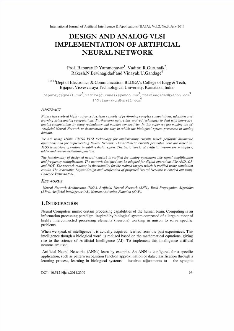
Dendrites: are branching fibers that extend from the cell body or soma. Soma or cell body of a
neuron contains the nucleus and other structures, support chemical processing and production of neurotransmitters.
Axon: It is a singular fiber carries information away from the soma to the synaptic sites of other neurons (dendrites and somas), muscles, or glands. Axon hillock is the site of summation
information. At any for incoming moment, the collective influence of all neurons that conductimpulses to a given neuron will determine whether or not an action potential will be initiated at
the axon hillock and propagated along the axon.
Axon Hillock
Soma
Dendrites
Myelin sheath
Synapse
Nucleus
Nodes of ranvier
Terminal buttonsAxon
Fig.1 Structure of Biological Neuron
Myelin Sheath: consists of fat-containing cells that insulate the axon from electrical activity.
This insulation acts to increase the rate of transmission of signals. A gap exists between each
8/6/2019 Design and Analog VLSI Implementation of Artificial Neural Network
http://slidepdf.com/reader/full/design-and-analog-vlsi-implementation-of-artificial-neural-network 3/14
International Journal of Artificial Intelligence & Applications (IJAIA), Vol.2, No.3, July 2011
98
myelin sheath cell along the axon. Since fat inhibits the propagation of electricity, the signals
jump from one gap to the next.
Nodes of Ranvier : are the gaps (about 1µm) between myelin sheath cells long axons are since
fat serves as a good insulator, the myelin sheaths speed the rate of transmission of an electrical
impulse along the axon.
Synapse: is the point of connection between two neurons or a neuron and a muscle or a gland.
Electrochemical communication between neurons takes place at these junctions.
Terminal Buttons: of a neuron are the small knobs at the end of an axon that release chemicalscalled neurotransmitters.
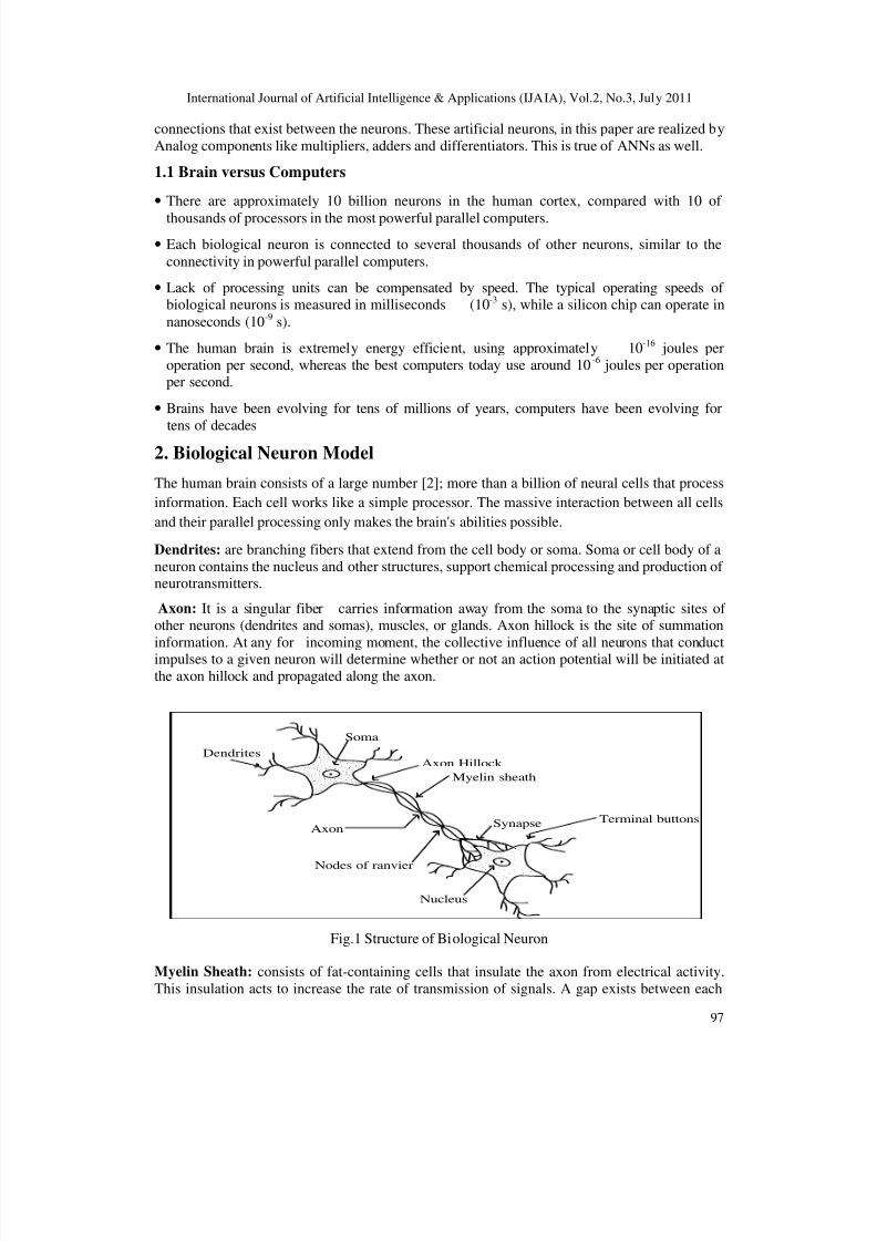
2.1 Artificial Neuron Model
An artificial neuron [2] is a mathematical function conceived as a simple model of a real(biological) neuron. This is a simplified model of real neurons, known as a Threshold Logic
Unit.
Vin1
W1
Vin2
W2
Vout
Fig.2 Mathematical model of Neuron
• A set of input connections brings in activations from other neurons.
• A processing unit sums the inputs, and then applies a non-linear activation function (i.e.
squashing / transfer / threshold function).
• An output line transmits the result to other neurons.
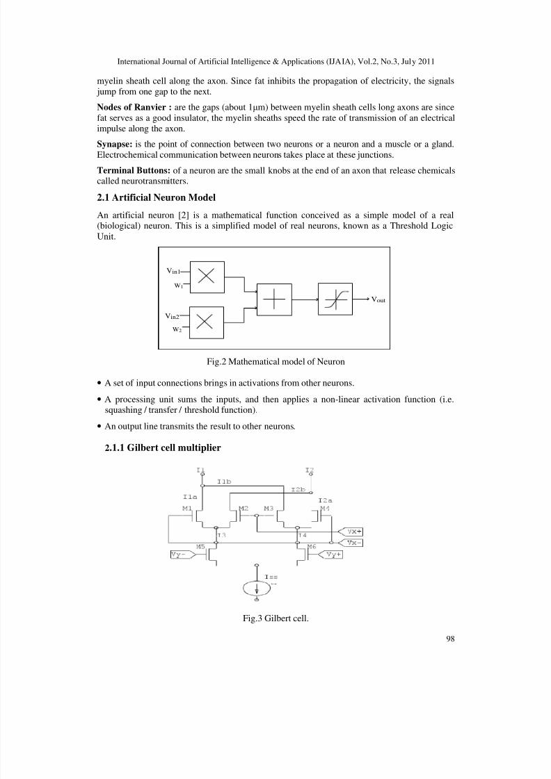
2.1.1 Gilbert cell multiplier
Fig.3 Gilbert cell.
8/6/2019 Design and Analog VLSI Implementation of Artificial Neural Network
http://slidepdf.com/reader/full/design-and-analog-vlsi-implementation-of-artificial-neural-network 4/14
International Journal of Artificial Intelligence & Applications (IJAIA), Vol.2, No.3, July 2011
99
In figure 4.3 the basic Gilbert cell structure is presented [1]. Assuming all transistors are biased
in the saturation region and obey the ideal square law equation and that devices are sized andmatched so that the transconductance parameters satisfy K1=K2=K3=K4=Ka and K5=K6=Kb.
Defining the output current I0=I2-I1=-(I2b+I2a)-(I1a+I1b), it can be shown that
If we demand
It follows that Io depends linearly on Vx
While the currents I3, I4 can be expressed as by
Substituting Vy and Io expression, it follows that
The output current yields an ideal analog multiplier [10]. Notice that since both I3 and I4 are ISS
and VY dependent, both VY and VX must be kept small to maintain good linearity.
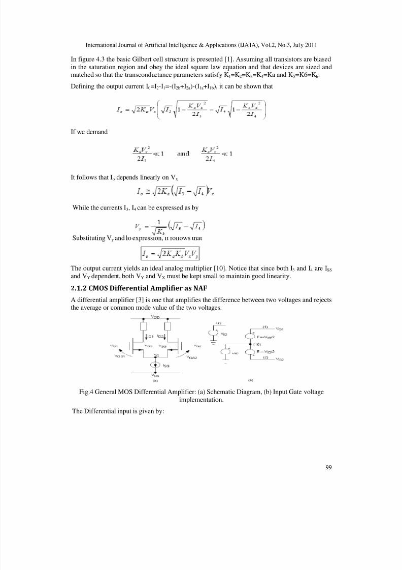
2.1.2 CMOS Differential Amplifier as NAF
A differential amplifier [3] is one that amplifies the difference between two voltages and rejectsthe average or common mode value of the two voltages.
Fig.4 General MOS Differential Amplifier: (a) Schematic Diagram, (b) Input Gate voltage
implementation. The Differential input is given by:
8/6/2019 Design and Analog VLSI Implementation of Artificial Neural Network
http://slidepdf.com/reader/full/design-and-analog-vlsi-implementation-of-artificial-neural-network 5/14
International Journal of Artificial Intelligence & Applications (IJAIA), Vol.2, No.3, July 2011
100
Two special cases of input gate signals are of interests: pure differential and pure common modeinput signals. Pure differential input signals mean V
IC=0, from equation (4) and (5);
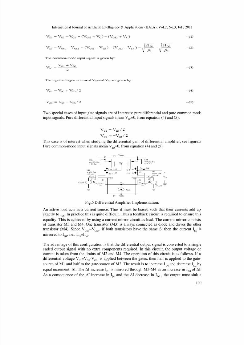
This case is of interest when studying the differential gain of differential amplifier, see figure.5
Pure common-mode input signals mean VID
=0, from equation (4) and (5);
Fig.5 Differential Amplifier Implementation: An active load acts as a current source. Thus it must be biased such that their currents add up
exactly to ISS
. In practice this is quite difficult. Thus a feedback circuit is required to ensure this
equality. This is achieved by using a current mirror circuit as load. The current mirror consistsof transistor M3 and M4. One transistor (M3) is always connected as diode and drives the other
transistor (M4). Since VGS3
=VGS4
, if both transistors have the same β, then the current ID3
is
mirrored to ID4
, i.e., ID3
=ID4
.
The advantage of this configuration is that the differential output signal is converted to a singleended output signal with no extra components required. In this circuit, the output voltage or
current is taken from the drains of M2 and M4. The operation of this circuit is as follows. If a
differential voltage VID
=VG1
-VG2
, is applied between the gates, then half is applied to the gate-
source of M1 and half to the gate-source of M2. The result is to increase ID1
and decrease ID2
by
equal increment, ∆I. The ∆I increase ID1
is mirrored through M3-M4 as an increase in ID4
of ∆I.
As a consequence of the ∆I increase in ID4
and the ∆I decrease in ID2
, the output must sink a
8/6/2019 Design and Analog VLSI Implementation of Artificial Neural Network
http://slidepdf.com/reader/full/design-and-analog-vlsi-implementation-of-artificial-neural-network 6/14
International Journal of Artificial Intelligence & Applications (IJAIA), Vol.2, No.3, July 2011
101
current of 2∆I. The sum of the changes in ID1
and ID2
at the common node VC
is zero. That is, the
node VC
is at an ac ground. From Eq (4) and Eq (5) for pure differential input signal means the
common-mode signal VIC
is zero. That is, the input signals are VG1
=VID /2 and V
G2=-V
ID /2. This
is shown in Figure.5. The transconductance of the differential amplifier is given by:
That is the differential amplifier has the same transconductance as a single stage commonsource amplifier.
Y
X
0
0
1.8V
-1.8V
-5 5
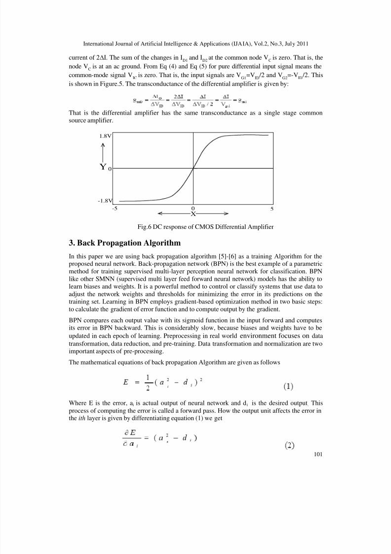
Fig.6 DC response of CMOS Differential Amplifier
3. Back Propagation Algorithm
In this paper we are using back propagation algorithm [5]-[6] as a training Algorithm for theproposed neural network. Back-propagation network (BPN) is the best example of a parametric
method for training supervised multi-layer perception neural network for classification. BPN
like other SMNN (supervised multi layer feed forward neural network) models has the ability tolearn biases and weights. It is a powerful method to control or classify systems that use data to
adjust the network weights and thresholds for minimizing the error in its predictions on thetraining set. Learning in BPN employs gradient-based optimization method in two basic steps:
to calculate the gradient of error function and to compute output by the gradient.
BPN compares each output value with its sigmoid function in the input forward and computesits error in BPN backward. This is considerably slow, because biases and weights have to be
updated in each epoch of learning. Preprocessing in real world environment focuses on data
transformation, data reduction, and pre-training. Data transformation and normalization are twoimportant aspects of pre-processing.
The mathematical equations of back propagation Algorithm are given as follows
Where E is the error, ai is actual output of neural network and di is the desired output. This
process of computing the error is called a forward pass. How the output unit affects the error inthe ith layer is given by differentiating equation (1) we get
8/6/2019 Design and Analog VLSI Implementation of Artificial Neural Network
http://slidepdf.com/reader/full/design-and-analog-vlsi-implementation-of-artificial-neural-network 7/14
International Journal of Artifi
The equation (2) can be written i
Where d(ai) is the differentiation
Where a1i is the output of the hi
rate. This error has to propagate
layer is calculated as
Weight update for the hidden la
(5) depend on the number of the
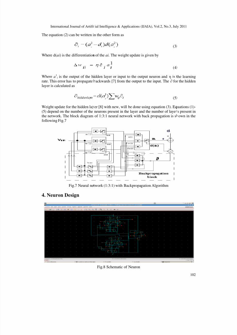
the network. The block diagramfollowing Fig.7
Fig.7 Neural ne
4. Neuron Design
ial Intelligence & Applications (IJAIA), Vol.2, No.3, Jul
n the other form as
(3
of the ai. The weight update is given by
(4
idden layer or input to the output neuron and η is
ackwards [7] from the output to the input. The ∂ fo
(5
er [8] with new, will be done using equation (3). Eq
neurons present in the layer and the number of laye
of 1:3:1 neural network with back propagation is s
twork (1:3:1) with Backpropagation Algorithm
Fig.8 Schematic of Neuron
y 2011
102
the learningr the hidden
uations (1)-
s present in
own in the
8/6/2019 Design and Analog VLSI Implementation of Artificial Neural Network
http://slidepdf.com/reader/full/design-and-analog-vlsi-implementation-of-artificial-neural-network 8/14
International Journal of Artifi
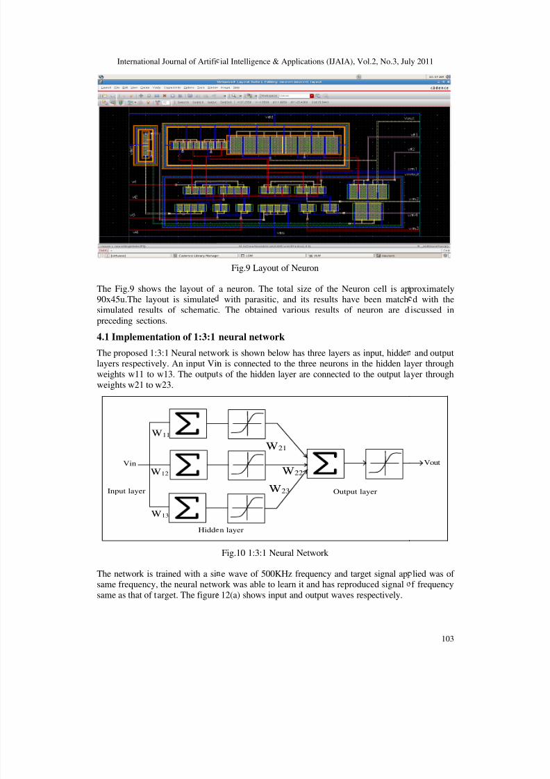
The Fig.9 shows the layout of 90x45u.The layout is simulatesimulated results of schematic
preceding sections.
4.1 Implementation of 1:3:1
The proposed 1:3:1 Neural netwlayers respectively. An input Vi
weights w11 to w13. The outpu
weights w21 to w23.
Vin
Input layer
Hidd
W11
W12
W13
The network is trained with a sisame frequency, the neural netw
same as that of target. The figure
ial Intelligence & Applications (IJAIA), Vol.2, No.3, Jul
Fig.9 Layout of Neuron
a neuron. The total size of the Neuron cell is apwith parasitic, and its results have been match
. The obtained various results of neuron are d
neural network
ork is shown below has three layers as input, hidden is connected to the three neurons in the hidden la
s of the hidden layer are connected to the output la
n layer
Output layer
W21
W22
W23
Fig.10 1:3:1 Neural Network
e wave of 500KHz frequency and target signal apork was able to learn it and has reproduced signal
12(a) shows input and output waves respectively.
y 2011
103
proximatelyd with theiscussed in
and outputyer through
yer through
Vout
lied was of f frequency
8/6/2019 Design and Analog VLSI Implementation of Artificial Neural Network
http://slidepdf.com/reader/full/design-and-analog-vlsi-implementation-of-artificial-neural-network 9/14
International Journal of Artifi
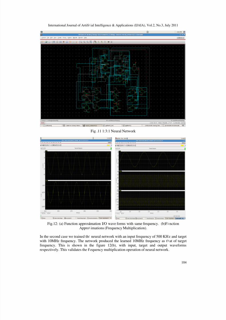
Fig.12: (a) Function approxiAppro
In the second case we trained th
with 10MHz frequency. The net
frequency. This is shown in
respectively. This validates the f
ial Intelligence & Applications (IJAIA), Vol.2, No.3, Jul
Fig .11 1:3:1 Neural Network
imation I/O wave forms with same frequency. (b)Fimations (Frequency Multiplication).
neural network with an input frequency of 500 KH
work produced the learned 10MHz frequency as t
the figure 12(b), with input, target and output
equency multiplication operation of neural network
y 2011
104
nction
z and target
at of target
waveforms
.
8/6/2019 Design and Analog VLSI Implementation of Artificial Neural Network
http://slidepdf.com/reader/full/design-and-analog-vlsi-implementation-of-artificial-neural-network 10/14
International Journal of Artifi
5. Analog Operations
5.1. Signal Amplification
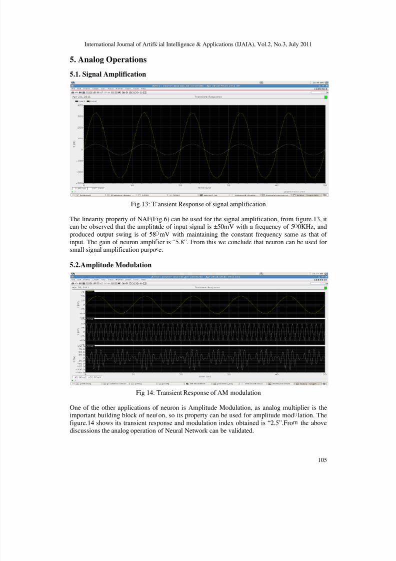
Fig.13: T
The linearity property of NAF(Fcan be observed that the amplitu
produced output swing is of 58
input. The gain of neuron amplismall signal amplification purpo
5.2.Amplitude Modulation
Fig 14:
One of the other applications oimportant building block of neu
figure.14 shows its transient res
discussions the analog operation
ial Intelligence & Applications (IJAIA), Vol.2, No.3, Jul
ansient Response of signal amplification
ig.6) can be used for the signal amplification, fromde of input signal is ±50mV with a frequency of 5
mV with maintaining the constant frequency sam
ier is “5.8”. From this we conclude that neuron cane.
Transient Response of AM modulation
f neuron is Amplitude Modulation, as analog multon, so its property can be used for amplitude mod
ponse and modulation index obtained is “2.5”.Fro
of Neural Network can be validated.
y 2011
105
figure.13, it0KHz, and
e as that of
be used for
iplier is thelation. The
the above
8/6/2019 Design and Analog VLSI Implementation of Artificial Neural Network
http://slidepdf.com/reader/full/design-and-analog-vlsi-implementation-of-artificial-neural-network 11/14
International Journal of Artifi
6. Digital Operations
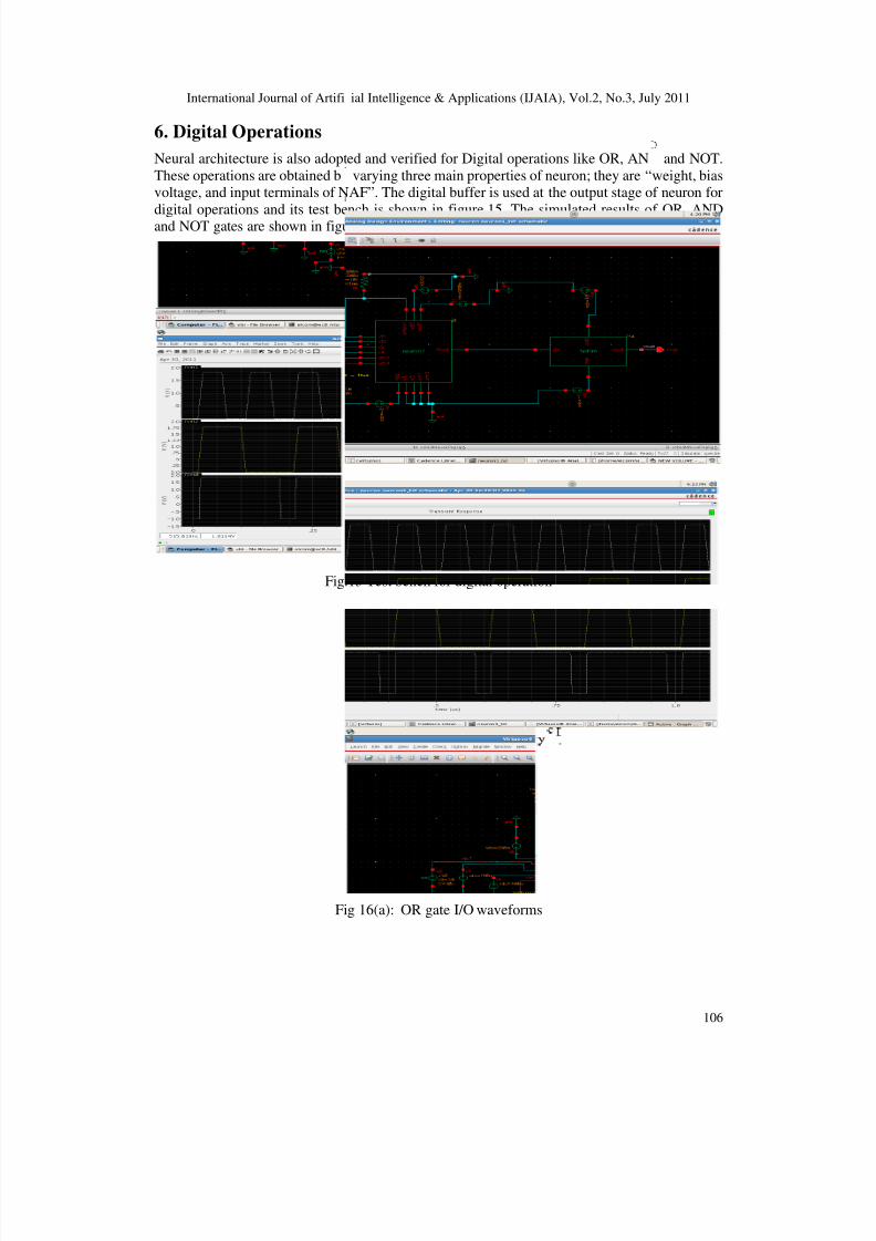
Neural architecture is also adopt
These operations are obtained bvoltage, and input terminals of N
digital operations and its test beand NOT gates are shown in figu
Fig.
Fi
ial Intelligence & Applications (IJAIA), Vol.2, No.3, Jul
ed and verified for Digital operations like OR, AN
varying three main properties of neuron; they are “AF”. The digital buffer is used at the output stage o
nch is shown in figure.15. The simulated results ore.16.
15 Test bench for digital operation
g 16(a): OR gate I/O waveforms
y 2011
106
and NOT.
weight, biasf neuron for
f OR, AND
8/6/2019 Design and Analog VLSI Implementation of Artificial Neural Network
http://slidepdf.com/reader/full/design-and-analog-vlsi-implementation-of-artificial-neural-network 12/14
International Journal of Artifi
Fi
6. Applications of Neura
Artificial neural networks are ostate explicit rules. Often it se
examples; if sufficient data is av
Clustering:
A clustering algorithm explorescluster. Best known applications
Classification/Pattern recognit
The task of pattern recognition ione of many classes. This cate
memory.
Function approximation:
The tasks of function approx
to noise. Various engineering an
ial Intelligence & Applications (IJAIA), Vol.2, No.3, Jul
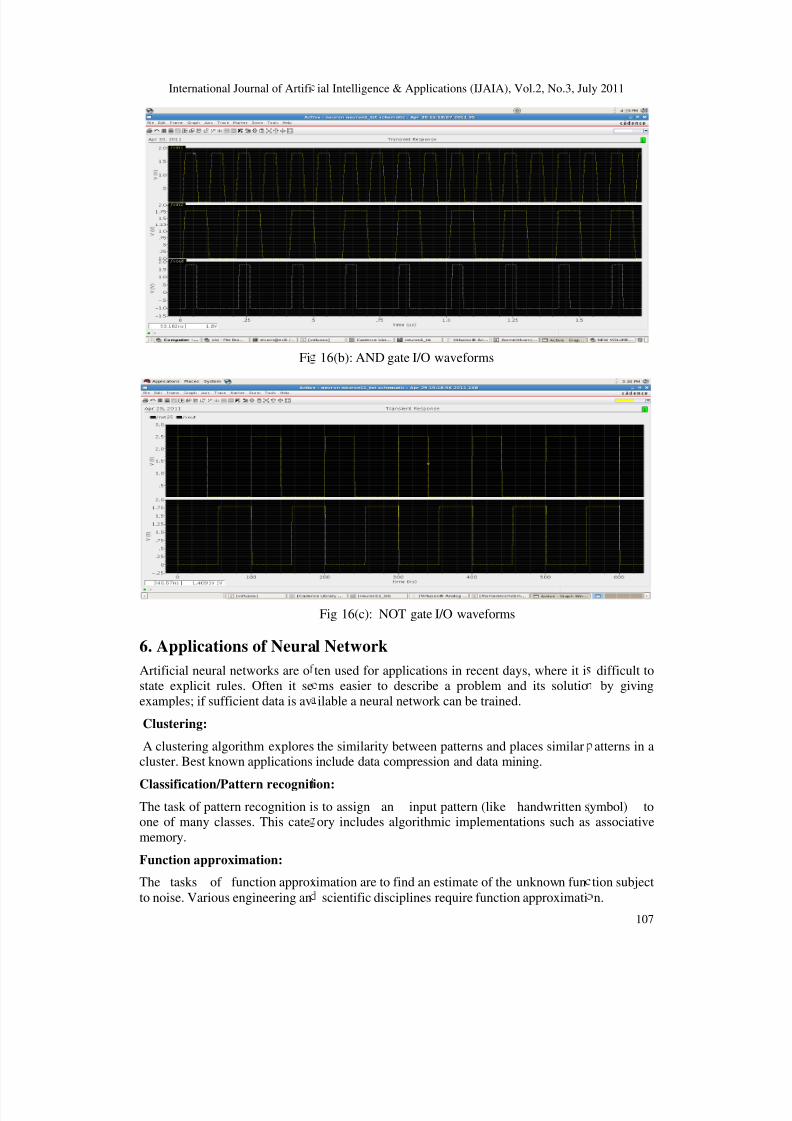
16(b): AND gate I/O waveforms
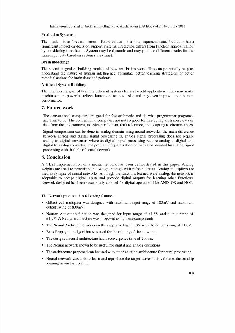
Fig 16(c): NOT gate I/O waveforms
l Network
ten used for applications in recent days, where it ims easier to describe a problem and its solutio
ilable a neural network can be trained.
the similarity between patterns and places similarinclude data compression and data mining.
ion:
s to assign an input pattern (like handwritten sory includes algorithmic implementations such as
imation are to find an estimate of the unknown fun
scientific disciplines require function approximati
y 2011
107
difficult toby giving
atterns in a
ymbol) toassociative
tion subject
n.
8/6/2019 Design and Analog VLSI Implementation of Artificial Neural Network
http://slidepdf.com/reader/full/design-and-analog-vlsi-implementation-of-artificial-neural-network 13/14
International Journal of Artificial Intelligence & Applications (IJAIA), Vol.2, No.3, July 2011
108
Prediction Systems:
The task is to forecast some future values of a time-sequenced data. Prediction has a
significant impact on decision support systems. Prediction differs from function approximationby considering time factor. System may be dynamic and may produce different results for the
same input data based on system state (time).
Brain modeling:
The scientific goal of building models of how real brains work. This can potentially help usunderstand the nature of human intelligence, formulate better teaching strategies, or better
remedial actions for brain damaged patients.
Artificial System Building:
The engineering goal of building efficient systems for real world applications. This may make
machines more powerful, relieve humans of tedious tasks, and may even improve upon human
performance.
7. Future work
The conventional computers are good for fast arithmetic and do what programmer programs,ask them to do. The conventional computers are not so good for interacting with noisy data ordata from the environment, massive parallelism, fault tolerance, and adapting to circumstances.
Signal compression can be done in analog domain using neural networks, the main difference
between analog and digital signal processing is, analog signal processing does not requireanalog to digital converter, where as digital signal processing require analog to digital and
digital to analog converter. The problem of quantization noise can be avoided by analog signal
processing with the help of neural network.
8. Conclusion
A VLSI implementation of a neural network has been demonstrated in this paper. Analogweights are used to provide stable weight storage with refresh circuit. Analog multipliers are
used as synapse of neural networks. Although the functions learned were analog, the network isadoptable to accept digital inputs and provide digital outputs for learning other functions.
Network designed has been successfully adopted for digital operations like AND, OR and NOT.
The Network proposed has following features.
Gilbert cell multiplier was designed with maximum input range of 100mV and maximum
output swing of 800mV.
Neuron Activation function was designed for input range of ±1.8V and output range of
±1.7V. A Neural architecture was proposed using these components.
The Neural Architecture works on the supply voltage ±1.8V with the output swing of ±1.6V.
Back Propagation algorithm was used for the training of the network.
The designed neural architecture had a convergence time of 200 ns.
The Neural network shown to be useful for digital and analog operations.
The architecture proposed can be used with other existing architecture for neural processing.
Neural network was able to learn and reproduce the target waves; this validates the on chip
learning in analog domain.
8/6/2019 Design and Analog VLSI Implementation of Artificial Neural Network
http://slidepdf.com/reader/full/design-and-analog-vlsi-implementation-of-artificial-neural-network 14/14
International Journal of Artificial Intelligence & Applications (IJAIA), Vol.2, No.3, July 2011
109
REFERENCES
[1]. Gilbert Multiplier by Ari Sharon, aris@cs, Ariel Zentner , relz@cs, Zachi Sharvit, zachi@cs,
Yaakov Goldberg, yaakov@cs.
[2]. Bose N. K., Liang P., “Neural Network Fundamentals with graphs, algorithms and Application”,
Tata McGraw hill, New Delhi, 2002, ISBN 0-07-463529-8
[3]. Razavi Behzad, “Design of Analog CMOS Integrated Circuits”, Tata McGrawhill, New
Delhi,2002, ISBN 0-07-052903-5
[4]. Bernabe Linares-Barranco et al., “A Modular T-Mode Design Approach for Analog
NeuralNetwork Hardware Implementations”, IEEE Journal of Solid-state Circuits. Vol. 27, no. 5,
May1992, pp. 701-713
[5]. Hussein CHIBLE, “Analysis And Design Of Analog Microelectronic Neural Network
Architectures With On-Chip Supervised Learning” Ph.D. Thesis in Microelectronics, University of
Genoa, 1997 Isik Aybay et al, “Classification of Neural Network Hardware”, Neural Network
World, IDG Co.,Vol 6 No 1, 1996, pp. 11-29
[6]. Vincent F. Koosh “Analog Computation and Learning in VLSI” PhD thesis California institute of
technology, Pasadena, California.2001
[7]. Roy Ludvig Sigvartsen, “An Analog Neural Network with On-Chip Learning” Thesis Department
of informatics, University of Oslo, 1994 Chun Lu, Bing-xue Shi and Lu Chen, “Hardware
Implementation of an Analog Accumulator for On-chip BP Learning Neural Networks” Institute of
Microelectronics, Tsinghua University Beijing, China 2002[8]. Arne Heittmann, “An Analog VLSI Pulsed Neural Network for Image Segmentation using,
Adaptive Connection Weights” Dresden University of Technology, Department of Electrical
[9]. European Journal of Scientific Research ISSN 1450-216X Vol.27 No.2 (2009), pp.199-216
[10]. Engineering and Information Technology, Dresden, Germany, 2000 Shai, Cai-Qin. Geiger, Randy
L. “A 5-v CMOS Analog Multiplier” IEEE Journal of solid state circuits Vol sc22 No.6 December
1987, pp. 1143-1146
Recommended

![Bidirectional Non-Filamentary RRAM as an Analog ... · on Neural Network Training Accuracy ... hardware. For a practical VLSI implementation, ... [11] for Deep Neural Networks (DNNs)](https://img.pdfslide.net/doc/110x75/5ac7918c7f8b9acb688bc18d/bidirectional-non-filamentary-rram-as-an-analog-neural-network-training-accuracy.jpg)