ECE 4600 Group Design Project
Design and Implementation of a DSTATCOM forPower Factor Correction
byGroup 06
Matthew Borody Bailey LavalleeNyasha Machoko Chantel Reyes
Final report submitted in partial satisfaction of the requirements for the degree of
Bachelor of Science in Electrical and Computer Engineering in the
Faculty of Engineering of the University of Manitoba
Academic Supervisor
Dr. Shaahin Filizadeh, Ph.D, P.Eng,Department of Electrical and Computer Engineering
University of Manitoba
Date of Submission
March 10, 2014
Copyright © 2014 Matthew Borody, Bailey Lavallee, Nyasha Machoko, Chantel Reyes

Design and Implementation of a DSTATCOM
Abstract
The purpose of this design project was to design and implement a solid-state device for
power factor correction. Power factor correction is an important consideration for utilities
and large power consumers as low power factor increases the ratings of distribution and
generation equipment resulting in large expense for both the provider and consumer. Our
system implemented a DSTATCOM employing a decoupled instantaneous current control
algorithm. The system was modelled and simulated in PSCAD prior to the implementation
of the design in hardware. The design was required to maintain unity power factor at all
times whilst keeping the total harmonic distortion below 5%. The active and reactive power
components of the system were required to act completely independently during changes in
the system. These goals were fully accomplished in simulation.
- ii -

Design and Implementation of a DSTATCOM
Contributions
Mat
thew
Bor
od
y
Bai
ley
Lav
alle
e
Nya
sha
Mac
hoko
Ch
ante
lR
eyes
Research • Simulation • • Parts Selection Signal Conditioning Circuits •PCB Design • Capacitor Charging Circuit Hardware Construction • dq0 Transform Algorithm •Software Clocking •PLL Algorithm •PWM Algorithm •Data Acquisition Algorithm •PID •Control Loop Algorithm System Construction and Implementation
Legend: • Lead task Contributed
- iii -

Design and Implementation of a DSTATCOM
Acknowledgements
Throughout the course of this project, there have been many people that have assisted us
in the theory, design, and construction, and we would like to thank the following:
Dr. Shaahin Filizadeh for creating the project and allowing us to take it on, and for his
guidance and advice at all stages. Mr. Erwin Dirks for being an invaluable resource and for
aiding us in learning how to properly carry out the hardware implementation; we thank him
for his time and patience as well as for the parts he provided. Dr. Ken Ferens for assisting
in Digital Signal Controller configuration as well as painstakingly sifting through source
code during our debugging process. Mr. Zoran Trajkoski for his help with, and advice and
lessons on PCB design and implementation. Mr. Cory Smit for cutting and drilling the
heat sink. Messrs. Alan McKay, Sinisa Janjic, Mount-First Ng, and Ken Biegun for the
time and resources expended and help provided on finding and ordering project parts, as
well as their assistance in the construction process. Mr. Warren Lavallee for building the
hardware enclosure and for his advice on project construction.
- iv -

Design and Implementation of a DSTATCOM TABLE OF CONTENTS
Table of Contents
Abstract . . . . . . . . . . . . . . . . . . . . . . . . . . . . . . . . . . . . . . . . . ii
Contributions . . . . . . . . . . . . . . . . . . . . . . . . . . . . . . . . . . . . . . iii
Acknowledgements . . . . . . . . . . . . . . . . . . . . . . . . . . . . . . . . . . . iv
List of Figures . . . . . . . . . . . . . . . . . . . . . . . . . . . . . . . . . . . . . vii
List of Tables . . . . . . . . . . . . . . . . . . . . . . . . . . . . . . . . . . . . . . ix
Glossary . . . . . . . . . . . . . . . . . . . . . . . . . . . . . . . . . . . . . . . . . x
1 Introduction 1
1.1 Motivation . . . . . . . . . . . . . . . . . . . . . . . . . . . . . . . . . . . . 1
1.2 Objective . . . . . . . . . . . . . . . . . . . . . . . . . . . . . . . . . . . . . 2
1.3 Project Definition and Specifications . . . . . . . . . . . . . . . . . . . . . . 2
1.4 Scope . . . . . . . . . . . . . . . . . . . . . . . . . . . . . . . . . . . . . . . 2
2 Theory 3
2.1 Introduction . . . . . . . . . . . . . . . . . . . . . . . . . . . . . . . . . . . . 3
2.1.1 Modelling of a DSTATCOM and Current Controller . . . . . . . . . 5
3 Transient Simulation of the DSTATCOM 10
3.1 System Overview . . . . . . . . . . . . . . . . . . . . . . . . . . . . . . . . . 10
3.2 Selection of DC link Capacitor . . . . . . . . . . . . . . . . . . . . . . . . . 11
3.3 Selection of Filtering Inductor . . . . . . . . . . . . . . . . . . . . . . . . . . 12
3.4 Simulation Results . . . . . . . . . . . . . . . . . . . . . . . . . . . . . . . . 13
4 Hardware 18
4.1 Introduction . . . . . . . . . . . . . . . . . . . . . . . . . . . . . . . . . . . . 18
4.2 Intelligent Power Module . . . . . . . . . . . . . . . . . . . . . . . . . . . . 18
4.3 Mounting . . . . . . . . . . . . . . . . . . . . . . . . . . . . . . . . . . . . . 20
4.4 Measurement and Isolation . . . . . . . . . . . . . . . . . . . . . . . . . . . 20
- v -

Design and Implementation of a DSTATCOM TABLE OF CONTENTS
4.5 Protection . . . . . . . . . . . . . . . . . . . . . . . . . . . . . . . . . . . . . 22
5 Software 24
5.1 Introduction . . . . . . . . . . . . . . . . . . . . . . . . . . . . . . . . . . . . 24
5.2 Digital Signal Controller . . . . . . . . . . . . . . . . . . . . . . . . . . . . . 24
5.2.1 Testing Setup . . . . . . . . . . . . . . . . . . . . . . . . . . . . . . . 25
5.3 Algorithms . . . . . . . . . . . . . . . . . . . . . . . . . . . . . . . . . . . . 26
5.3.1 Initialization . . . . . . . . . . . . . . . . . . . . . . . . . . . . . . . 27
5.3.2 Data Acquisition . . . . . . . . . . . . . . . . . . . . . . . . . . . . . 29
5.3.3 Park’s Transformations . . . . . . . . . . . . . . . . . . . . . . . . . 31
5.3.4 PI Control . . . . . . . . . . . . . . . . . . . . . . . . . . . . . . . . 32
5.3.5 Pulse-Width Modulation . . . . . . . . . . . . . . . . . . . . . . . . . 34
5.3.6 Phase-Locked Loop . . . . . . . . . . . . . . . . . . . . . . . . . . . . 36
5.4 Conclusion . . . . . . . . . . . . . . . . . . . . . . . . . . . . . . . . . . . . 40
6 Implementation 41
6.1 Intelligent Power Module Set-up . . . . . . . . . . . . . . . . . . . . . . . . 41
6.2 Lab-Volt Set-up . . . . . . . . . . . . . . . . . . . . . . . . . . . . . . . . . . 42
6.3 Results . . . . . . . . . . . . . . . . . . . . . . . . . . . . . . . . . . . . . . . 44
7 Conclusions 45
7.1 Future Work . . . . . . . . . . . . . . . . . . . . . . . . . . . . . . . . . . . 45
References 47
Appendix A Project Notes 49
Appendix B Budget Summary 58
Appendix C Figures 60
Appendix D Curriculum Vitae 61
- vi -

Design and Implementation of a DSTATCOM LIST OF FIGURES
List of Figures
2.1 A simplified model of a DSTATCOM . . . . . . . . . . . . . . . . . . . . . . 5
2.2 d-axis control loop . . . . . . . . . . . . . . . . . . . . . . . . . . . . . . . . 8
2.3 q-axis control loop . . . . . . . . . . . . . . . . . . . . . . . . . . . . . . . . 9
3.1 DSTATCOM system diagram . . . . . . . . . . . . . . . . . . . . . . . . . . 11
3.2 Uncompensated Phase A source voltage (green) and current (blue) . . . . . 13
3.3 DSTATCOM connected to grid; blue: capacitor voltage, red: source current,
green: source voltage . . . . . . . . . . . . . . . . . . . . . . . . . . . . . . . 14
3.4 Transient response with Capacitor pre-charged; blue: capacitor voltage, red:
source current, green: source voltage . . . . . . . . . . . . . . . . . . . . . . 15
3.5 DSTATCOM phase A current with capacitor pre-charged; blue: DSTAT-
COM current, green: capacitor voltage . . . . . . . . . . . . . . . . . . . . . 16
3.6 DSTATCOM harmonics . . . . . . . . . . . . . . . . . . . . . . . . . . . . . 16
3.7 DSTATCOM in capacitive and inductive mode; blue: q component, green: d
component . . . . . . . . . . . . . . . . . . . . . . . . . . . . . . . . . . . . 17
3.8 Source voltage and current with load being changed to capacitive from in-
ductive; blue: capacitor voltage, green: source voltage, red: source current . 17
4.1 PCB final design . . . . . . . . . . . . . . . . . . . . . . . . . . . . . . . . . 21
4.2 Potential signal conditioning circuit . . . . . . . . . . . . . . . . . . . . . . . 22
5.1 Test setup for dsPIC33FJ16GS402 . . . . . . . . . . . . . . . . . . . . . . . 25
5.2 portInit subroutine . . . . . . . . . . . . . . . . . . . . . . . . . . . . . . . . 28
5.3 Oscilloscope image of clock speed test . . . . . . . . . . . . . . . . . . . . . 29
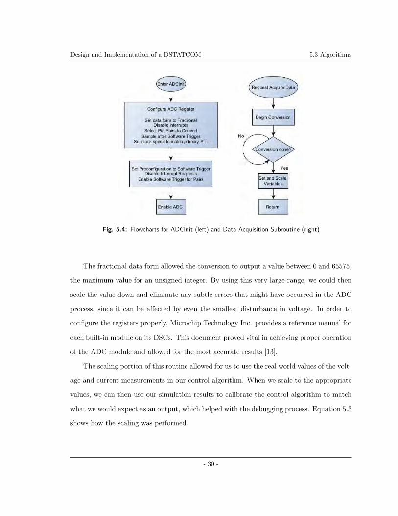
5.4 Flowcharts for ADCInit (left) and Data Acquisition Subroutine (right) . . . 30
5.5 d and q components of Park’s transformation in MATLAB . . . . . . . . . 32
5.6 Three-phase components of inverse transformation in MATLAB . . . . . . . 33
- vii -

Design and Implementation of a DSTATCOM LIST OF FIGURES
5.7 PI Response to a step input . . . . . . . . . . . . . . . . . . . . . . . . . . . 34
5.8 SPWM module configuration . . . . . . . . . . . . . . . . . . . . . . . . . . 35
5.9 Unit test for PWM . . . . . . . . . . . . . . . . . . . . . . . . . . . . . . . . 36
5.10 ZCD circuit schematic . . . . . . . . . . . . . . . . . . . . . . . . . . . . . . 37
5.11 PLL in PSCAD . . . . . . . . . . . . . . . . . . . . . . . . . . . . . . . . . . 38
5.12 Flowcharts for PLL . . . . . . . . . . . . . . . . . . . . . . . . . . . . . . . . 39
5.13 PLL locked to peaks of source voltage . . . . . . . . . . . . . . . . . . . . . 39
6.1 Output waveform across phase A and B . . . . . . . . . . . . . . . . . . . . 42
6.2 Lab-Volt test set-up; A: phase-A source voltage, B: DSTATCOM current
measurement, C: load current measurement . . . . . . . . . . . . . . . . . . 43
6.3 Hardware Configuration: a) Signal Conditioning circuits; b) DSC; c) Mea-
surement Board; d) PCB and Control connections e) Inductors f) Capacitor
and discharge switch . . . . . . . . . . . . . . . . . . . . . . . . . . . . . . . 43
C.1 PCB electrical connections in Multisim . . . . . . . . . . . . . . . . . . . . . 60
- viii -
Design and Implementation of a DSTATCOM LIST OF TABLES
List of Tables
1.1 Specifications . . . . . . . . . . . . . . . . . . . . . . . . . . . . . . . . . . . 2
5.1 Algorithms . . . . . . . . . . . . . . . . . . . . . . . . . . . . . . . . . . . . 27
5.2 Simplified truth table of IGBT switch vs. PWM input state [1] . . . . . . . 36
A.1 Original specifications (set 2014-09-27) . . . . . . . . . . . . . . . . . . . . . 49
- ix -

Design and Implementation of a DSTATCOM LIST OF TABLES
Glossary
Term Description
CT Current Transformer
DSC Digital Signal Controller
DSTATCOM Distribution Static Compensator
FACTS Flexible Alternating Current Transmission System
GPIO General Purpose Input Output
I/O Input/Output
IC Integrated Circuit
IGBT Insulated-Gate Bipolar Transistor
IPM Intelligent Power Module
MCU Microcontroller Unit
PLL Phase-Locked Loop
PCC Point of Common Coupling
PT Potential Transformer
PCB Printed Circuit Board
PI Proportional-Integral
SISO Single-Input Single-Output
SPWM Sinusoidal Pulse-Width Modulation
THD Total Harmonic Distortion
VSC Voltage Source Converter
ZCD Zero-Crossing Detector
- x -

Design and Implementation of a DSTATCOM 1. Introduction
Chapter 1
Introduction
This project was completed for the ECE4600 Group Design Project course at the Univer-
sity of Manitoba. This section includes the project’s motivation, objectives, and design
specifications.
1.1 Motivation
Power factor correction at distribution level is an important consideration for large con-
sumers and utilities. By definition, power factor is the ratio of active power (W) to appar-
ent power (VA). A low power factor causes inefficiencies in the electrical supply network by
forcing utilities to increase the VA rating of their switchgear and distribution transform-
ers in order to supply more reactive power. In the past, utilities used capacitor banks for
power factor correction, but they have proven bulky and inflexible. The advent of Flexible
Alternating Current Transmission System (FACTS) controllers such as the DSTATCOM
(Distribution Static Compensator) has paved the way for more efficient and flexible methods
of reactive power compensation.
- 1 -

Design and Implementation of a DSTATCOM 1.2 Objective
1.2 Objective
The goal of this project was to design and implement a solid-state device for power factor
correction. This was accomplished through the use of a DSTATCOM, which includes a
six-pulse Voltage Source Converter (VSC) employing Insulated-Gate Bipolar Transistors
(IGBT) and controlled by a decoupled instantaneous current controller method.
1.3 Project Definition and Specifications
The only constraint for this project was to develop a solid-state device. Our original specifi-
cations were as outlined in Table A.1 in Appendix A, however due to hardware availability,
the specification had to be modified as shown in Table 1.1. The project budget summary
can be found in Appendix B.
Table 1.1: Specifications
Description Requirement
Source Voltage 120/208V, 5A
Load 120/208V, 2.5A, 350W wound-rotor induction motor
Total Harmonic Distortion (THD) < 5%
Switching Hardware Insulated-Gate Bipolar Transistor (IGBT)
Switching Frequency 15kHz
1.4 Scope
We have chosen to implement the DSTATCOM for the purpose of reactive power compen-
sation, however the control algorithm can be modified to correct voltage sag as well. Our
design is equipped to operate under stable lab conditions, and is not suitable for connection
to uncontrolled sources.
- 2 -

Design and Implementation of a DSTATCOM 2. Theory
Chapter 2
Theory
2.1 Introduction
The DSTATCOM is a FACTS controller consisting of a voltage source converter connected
to a DC link capacitor at its input. The VSC is capable of generating 3-phase balanced
sinusoidal voltages from the constant DC voltage on the capacitor. The phase and frequency
of the generated 3-phase voltages are controllable, allowing the DSTATCOM to act like
an ideal synchronous condenser with a very fast response [2]. When the DSTATCOM
is connected in shunt with the active AC grid, the DSTATCOM can act as a controlled
reactive power source. The equations governing active and reactive power-flow between the
DSTATCOM and the grid are given by:
P =
(V2sin(φ)
X
)V1 (2.1a)
Q =
(V2cos(φ) − V1
X
)V1 (2.1b)
- 3 -

Design and Implementation of a DSTATCOM 2.1 Introduction
where V1 is the voltage of the active AC system, V2 is the voltage at the output of the
DSTATCOM, X is the reactance between the DSTATCOM and the AC grid, and φ is
the phase angle between V1 and V2. As shown in Equations 2.1a and 2.1b, exchange of
reactive and real power is achieved by controlling the amplitude of the VSC output voltage.
When the DSTATCOM and the grid have the same voltage and the same phase, there is
no reactive power exchange. When the voltage output of the DSTATCOM is higher than
that of the grid, reactive power will be injected into the system by the DSTATCOM, and
it acts like a capacitor. When the voltage output of the DSTATCOM is lower than that of
the grid, reactive power is absorbed by the DSTATCOM, and it acts like an inductor.
In our application, the DSTATCOM is used as a reactive power compensator. As such,
the angle between V1 and V2 is 0 [3]. Since φ is zero, the real power exchange between
DSTATCOM and the grid is zero. However, since the DC link capacitor is not supported
by an active DC source, there will be a small real power exchange between the grid and the
DSTATCOM in order to maintain the voltage on the capacitor.
There are many ways of controlling the DSTATCOM to achieve reactive power compen-
sation. The easiest method involves measuring the reactive power in the system and then
increasing or decreasing the voltage output of the VSC until unity power factor correction
is achieved. This control algorithm was considered and rejected because it would result in
uncontrollable transients above our system rating when there is a perturbation in the load.
After literature review of DSTATCOM control algorithms, we decided on the decoupled
instantaneous current control method. We chose this control algorithm because it allowed
us independent control of the active and reactive power in the DSTATCOM. This control
algorithm also employs components which we are very familiar with such as Proportional-
Integral (PI) controllers and Sinusoidal Pulse-Width Modulation (SPWM). A fixed VSC
switching frequency and self-supporting DC bus were two other advantages to this control
- 4 -
Design and Implementation of a DSTATCOM 2.1 Introduction
structure [4].
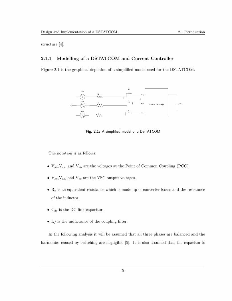
2.1.1 Modelling of a DSTATCOM and Current Controller
Figure 2.1 is the graphical depiction of a simplified model used for the DSTATCOM.
Fig. 2.1: A simplified model of a DSTATCOM
The notation is as follows:
• Vsa,Vsb, and Vsb are the voltages at the Point of Common Coupling (PCC).
• Vca,Vcb, and Vcc are the VSC output voltages.
• Rs is an equivalent resistance which is made up of converter losses and the resistance
of the inductor.
• Cdc is the DC link capacitor.
• Lf is the inductance of the coupling filter.
In the following analysis it will be assumed that all three phases are balanced and the
harmonics caused by switching are negligible [5]. It is also assumed that the capacitor is
- 5 -

Design and Implementation of a DSTATCOM 2.1 Introduction
ideal. Using principles from basic circuit theory analysis, the inverter output voltage can
be derived as:
Vca = Rsia + Lfdiadt
+ Vsa (2.2a)
Vcb = Rsib + Lfdibdt
+ Vsb (2.2b)
Vcc = Rsic + Lfdicdt
+ Vsc (2.2c)
The above equations can be rearranged in matrix form as:
d
dt
ia
ib
ic
=
RsLf
0 0
0 RsLf
0
0 0 RsLf
ia
ib
ic
+1
Lf
Vsa − Vca
Vsb − Vcb
Vsc − Vcc
(2.3)
The above matrix can be transformed from the ABC to dq0 coordinates by employing
the power-invariant Park transformation given in Equation 2.4.
ud
uq
u0
=
√2
3
cos(θ) cos(θ − 2π
3 ) cos(θ + 2π3 )
−sin(θ) −sin(θ − 2π3 ) −sin(θ + 2π
3 )
1√2
1√2
1√2
ua
ub
uc
(2.4)
Transforming Equation 2.3 into dq0 coordinates results in Equations (2.5a) and (2.5b).
Lfdicqdt
= −Rsicq − wLf icd + Vsq + Vcq (2.5a)
Lfdicddt
= −Rsicd + wLf icq + Vsd − Vcd (2.5b)
According to the Instantaneous Reactive Power Theory, the reactive and active power
- 6 -

Design and Implementation of a DSTATCOM 2.1 Introduction
in the dq0 frame can be written as:
p = vsdid + vsqid (2.6a)
q = vsqid − vsdiq (2.6b)
The dq0 transformation is the projection of 3-phase time domain signals into a syn-
chronous rotating two axis frame. In our DSTATCOM, the synchronous rotating frame is
aligned 90 to the grid source voltage. When the synchronous rotating frame is aligned to
the source voltage, it can be shown that the q-axis component of the source voltage is zero
[2]. As a result the active and reactive power becomes:
p = vsdid (2.7a)
q = −vsdiq (2.7b)
From Equations (2.7a) and (2.7b) it can be seen that the active and reactive power in
the DSTATCOM can be independently controlled through id and iq, respectively. However,
equations (2.5a) and (2.5b) indicate that id and iq cannot be independently controlled. They
are coupled together via the inductance of the coupling filter. To independently control
the active and reactive power in the DSTATCOM, a decoupling strategy was adopted. The
DSTATCOM can be decoupled by configuring the inputs being given to the VSC via SPWM
as [5]:
V ∗oq = Vsq − wLf icd − Vcq (2.8a)
V ∗od = Vsd + wLf icq − Vcd (2.8b)
From equations (2.8a) and (2.8b) we find the following Single-Input Single-Output
- 7 -

Design and Implementation of a DSTATCOM 2.1 Introduction
(SISO) system:
d
dt
icqicd
=
RsLf
0
0 −RsLf
icdicq
+1
Lf
V ∗oqV ∗od
(2.9)
The DC link capacitor in our DSTATCOM is self-supporting and the voltage across it
has to be kept constant. To accomplish this, a very small active power exchange occurs
between the AC grid and the DSTATCOM to compensate for the power losses caused by
equivalent resistances in the DSTATCOM [6]. To achieve the active power exchange, the
control system uses two PI controllers as shown in Figure 2.2. The first PI controller takes
as input the error between reference DC voltage and the measured voltage on the DC
link capacitor. The output of the PI controller is taken as the reference icd current. The
reference icd is then compared to the measured icd (DSTATCOM d-axis current); the error
between the two is fed to a second PI controller and the output of that PI controller is Vcd.
Equations (2.8a) and (2.8b) are used to decouple active and reactive power.
Fig. 2.2: d-axis control loop
The main objective of our DSTATCOM is to act as a reactive power compensator. This
is achieved by monitoring the q-axis component of load current and comparing it to the
- 8 -

Design and Implementation of a DSTATCOM 2.1 Introduction
q-axis current of the DSTATCOM, as shown in Figure 2.3. The difference between these
two is fed to a PI controller and the output is treated as Voq. Equation (2.8a) is then used to
decouple the active and reactive power in the DSTATCOM. The outputs from these control
loops, V∗oq and V∗od are put through the inverse Park transform to form the PWM carrier
waveform. The VSC produces the voltage requested by the controller to achieve reactive
power compensation.
Fig. 2.3: q-axis control loop
- 9 -

Design and Implementation of a DSTATCOM 3. Transient Simulation of the DSTATCOM
Chapter 3
Transient Simulation of the
DSTATCOM
The DSTATCOM was simulated in order to verify the current controller functionality and to
define steady state and transient characteristics of the system. The simulation environment
of choice was PSCAD.
3.1 System Overview
Figure 3.1 shows the high level block diagram of the entire system. This model directly
correlates to the PSCAD model and will be discussed in the following sections.
- 10 -

Design and Implementation of a DSTATCOM 3.2 Selection of DC link Capacitor
Fig. 3.1: DSTATCOM system diagram
3.2 Selection of DC link Capacitor
There were two main considerations when choosing the capacitor: it was required to be
large enough to supply the VSC with a sufficiently stable DC voltage in order to avoid
high harmonics in the DSTATCOM AC voltage output [7], and had to be able to supply
the system with the required reactive power for power factor compensation. An undersized
capacitor will result in high harmonics in the DSTATCOM AC voltage output [8], but an
oversized capacitor will result in a slower response time for the DC link controller. Using
Equation 3.1 where VDC is the DC bus voltage (350V), VDC1 is the minimum DC voltage,
V is the phase voltage, a is the overloading factor (1.2), I is the phase current, t is the
DC voltage recovery time, and CDC is the desired value, we were able to calculate the
capacitance to be approximately 2100µF.
- 11 -
Design and Implementation of a DSTATCOM 3.3 Selection of Filtering Inductor
1
2CDC [(VDC)2 − (V 2
DC1)] = 3V aIt (3.1)
When choosing a capacitor for purchase, we had to be especially conscious that the
chosen capacitor not only met the requirements stipulated during calculation, but also had
a sufficiently high current ripple rating. We purchased a 2200µF capacitor which was within
our budget, and met or exceeded all necessary criteria.
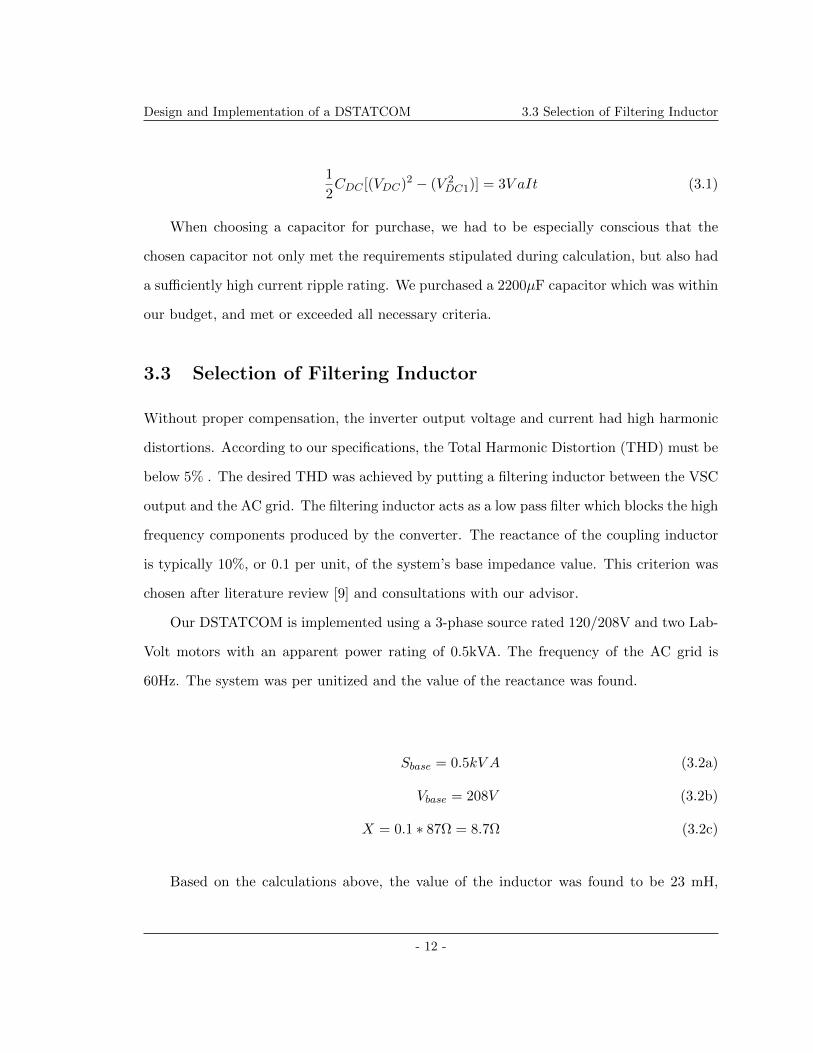
3.3 Selection of Filtering Inductor
Without proper compensation, the inverter output voltage and current had high harmonic
distortions. According to our specifications, the Total Harmonic Distortion (THD) must be
below 5% . The desired THD was achieved by putting a filtering inductor between the VSC
output and the AC grid. The filtering inductor acts as a low pass filter which blocks the high
frequency components produced by the converter. The reactance of the coupling inductor
is typically 10%, or 0.1 per unit, of the system’s base impedance value. This criterion was
chosen after literature review [9] and consultations with our advisor.
Our DSTATCOM is implemented using a 3-phase source rated 120/208V and two Lab-
Volt motors with an apparent power rating of 0.5kVA. The frequency of the AC grid is
60Hz. The system was per unitized and the value of the reactance was found.
Sbase = 0.5kV A (3.2a)
Vbase = 208V (3.2b)
X = 0.1 ∗ 87Ω = 8.7Ω (3.2c)
Based on the calculations above, the value of the inductor was found to be 23 mH,
- 12 -

Design and Implementation of a DSTATCOM 3.4 Simulation Results
however due to supplier availability, we purchased 28mH inductors as they exceeded the
required value.
3.4 Simulation Results
Figure 3.2 shows the source voltage and current for phase A without the DSTATCOM
connected. The source is connected to a three phase load with a 0.58 lagging power factor.
Fig. 3.2: Uncompensated Phase A source voltage (green) and current (blue)
Figure 3.3 shows the DC link capacitor voltage and phase A source voltage and current
with the DSTATCOM connected. The source current is scaled by a factor of 10 so that it
can be easily seen. Unity power factor correction is achieved 0.2s after system start-up. The
reference DC link capacitor voltage is 350V with a settling time of 0.2s and percent overshoot
of 26%. However, the transient response of the source current when the DSTATCOM is
connected shows sustained overcurrents lasting for approximately 0.18s. This is caused by
- 13 -

Design and Implementation of a DSTATCOM 3.4 Simulation Results
Fig. 3.3: DSTATCOM connected to grid; blue: capacitor voltage, red: source current,green: source voltage
inrush currents which occur when the DC link capacitor is initially charged by the system.
During implementation of the DSTATCOM, these overcurrents would be a problem since
the Lab-Volt equipment being used is not designed to withstand overcurrents of such a
magnitude lasting for more than 10 cycles. This led us to pre-charge the capacitor before
turning on the DSTATCOM.
Pre-charging the capacitor helped to reduce both magnitude and duration of the over-
currents in the system. The response of the DC link capacitor voltage became a 1st order
response.
The transient DSTATCOM current before the capacitor was pre-charged looked very
much like the transients of the source current. Pre-charging the DC link capacitor helps to
reduce the magnitude and duration of the transient currents in the DSTATCOM, as shown
in Figures 3.4 and 3.5.
- 14 -

Design and Implementation of a DSTATCOM 3.4 Simulation Results
Fig. 3.4: Transient response with Capacitor pre-charged; blue: capacitor voltage, red:source current, green: source voltage
Figure 3.6 shows harmonic spectrum of the DSTATCOM current. We only have the
fundamental in the first 30 harmonics. The THD we calculated for our DSTATCOM current
was 1.03%; this is below the required 5% we stated in our specifications.
One of the reason we chose the this control algorithm was because it allowed us to
independently control the active and reactive power in the DSTATCOM. In Figure 3.7, at
0.4s the load is switched from inductive to capacitive. As shown in the figure, there is no
disturbance in the active power component of the DSTATCOM which is given by the current
Dd, however, the reactive power component of the DSTATCOM smoothly transitioned from
inductive mode to capacitive mode.
Figure 3.8 shows the capacitor voltage, and source voltage and current. At 0.4s, the
load is changed from inductive to capacitive. As we can see, the system instantaneously
compensates for the capacitive load without any transients.
- 15 -

Design and Implementation of a DSTATCOM 3.4 Simulation Results
Fig. 3.5: DSTATCOM phase A current with capacitor pre-charged; blue: DSTATCOMcurrent, green: capacitor voltage
Fig. 3.6: DSTATCOM harmonics
- 16 -

Design and Implementation of a DSTATCOM 3.4 Simulation Results
Fig. 3.7: DSTATCOM in capacitive and inductive mode; blue: q component, green: dcomponent
Fig. 3.8: Source voltage and current with load being changed to capacitive from inductive;blue: capacitor voltage, green: source voltage, red: source current
- 17 -
Design and Implementation of a DSTATCOM 4. Hardware
Chapter 4
Hardware
4.1 Introduction
We divided the hardware section of the project into two subsections: the Intelligent
Power Module (IPM) and included peripherals, and the DSC peripherals. The IPM section
included all the connections made to the IPM such as the isolation, fuses, filtering inductors,
capacitor, and resistive divider for capacitor voltage measurement. The DSC peripherals
included circuits for the current and voltage signal conditioning, and the ZCD circuit.
We decided to use Lab-Volt equipment for our source and load; the load being comprised
of two 3-phase wound-rotor induction motors. We also had to consider how we would
connect to the source, load, and potential and current transformers. Having this knowledge
in the beginning of the hardware implementation stage meant we were able to account for
these connections throughout the planning and construction of the hardware components.
4.2 Intelligent Power Module
The inverter is one of the main parts of our system. There are many advantages to
using a module such as the IPM: it has an internal gate-driver which eliminates the need for
- 18 -

Design and Implementation of a DSTATCOM 4.2 Intelligent Power Module
us to design and build one externally, and the six IGBTs included in the IPM ensured that
they were identical and we would not run into any issues with manufacturing differences.
The IPM also includes a configurable smart shutdown function which effectively disables
the IPM in the event of an overcurrent. Though useful in many applications, because of
the protective measures we took while designing the system, we decided to disable it as it
was unneeded and would introduce unnecessary complications to the IPM set-up.
One of the first things we had to consider when setting up the IPM was the bootstrap
capacitors. Bootstrap capacitors are used to allow for a potential to exist across the in-
verter’s high switches to enable them to turn on and off. An IPM application guide written
by STM provides a capacitor selection diagram based on the value Vcboot (the minimum
allowable voltage drop across the high switch to indicate the high voltage side as on) and
the switching frequency. From this graph, we were able to obtain a bootstrap capacitance
of 1µF based on our 15kHz switching frequency and desired 0.1V drop [10].
Another component of major importance to us was the heat sink for the IPM. Since we
are switching at a high frequency (15kHz), it was of vital importance that the heat generated
by the IPM be dissipated. After a consultation with the ECE Department technical staff,
we were able to get a heat sink from the department appropriately sized for our application.
One feature of this IPM is how it handles the IGBT gate control pulses. Instead of
accepting six different pulse trains (three trains 120 out of phase with one another, and
inverted trains to make up the other three), it accepts three and performs the inversion
internally [1]. This set-up prevents the IGBT bridge from shorting in the event of micro-
controller failure.
Though the IPM offers many advantages, one of the disadvantages of this module lied
in its non-standard pin size and spacing. Though this small disadvantage was outweighed
by the features offered by the IPM, it did require a PCB be made in order to mount the
module.
- 19 -
Design and Implementation of a DSTATCOM 4.3 Mounting
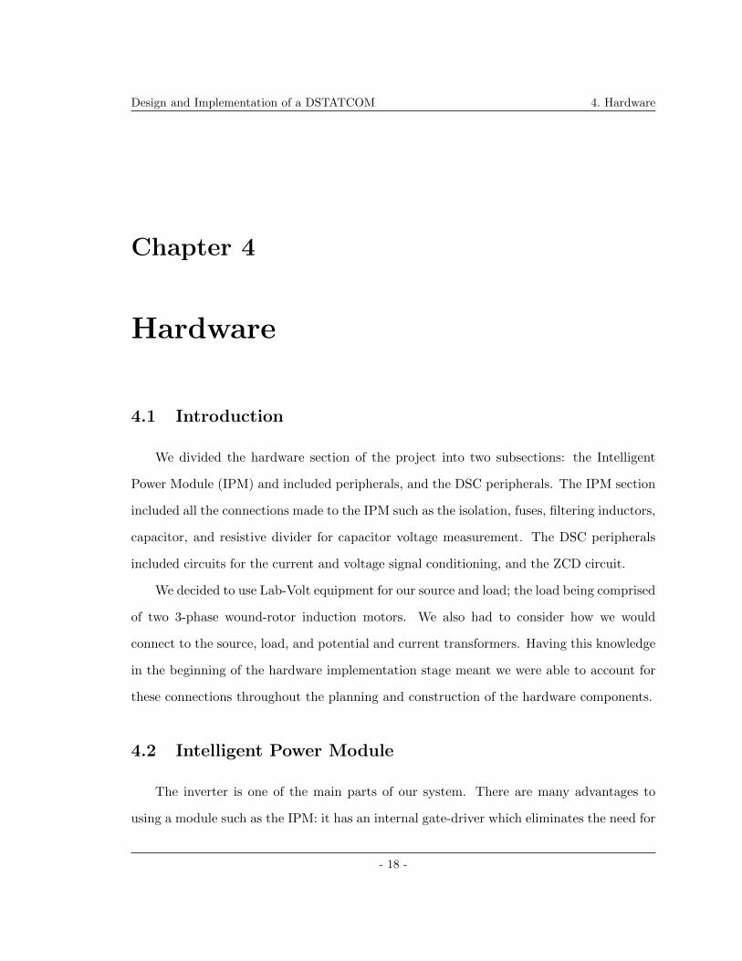
4.3 Mounting
The first step in the PCB design process was to map out all the parts that would be
included on the PCB and the connections between them. The PCB included all parts on
the high side of the isolation: IPM and bootstrap capacitors, resistive divider, and fuses.
Initially, we planned to mount the capacitor and inductors on the PCB as well, however
it was impractical and expensive. As a result, we included terminal strips to allow for
connection to the capacitor, and to and from the inductors. This set-up allowed us to
connect the capacitor to the upper and lower DC bus, and to make a connection from the
IPM output to the inductors, and back again to the PCB to connect to the fuses. The fuses
then feed to a terminal strip which allows the DSTATCOM to connect to the grid.
Once all the required internal and external connections were planned, we were able to
begin creating footprints for each of the required parts. We chose to use a combination of
Multisim and Ultiboard to design the PCB due to software availability and familiarity. The
PCB electrical connections were made in Multisim, as shown in Figure C.1 in Appendix C.
Upon completion of the electrical connections in Multisim, the diagram was transferred to
Ultiboard and the components were then arranged keeping in mind the need to keep the
board as small as possible to reduce costs.
The final PCB design is shown in Figure 4.1.
4.4 Measurement and Isolation
The current controller in our DSTATCOM was implemented using a DSC, which required
we safely step down and level shift all measured quantities to a level the DSC can handle.
Our current control algorithm requires source voltage, load current, DSTATCOM current,
and the DC link voltage. The AC signals are acquired using potential transformers and
current transformers. We chose PTs and CTs because they are readily available from the
- 20 -
Design and Implementation of a DSTATCOM 4.4 Measurement and Isolation
Fig. 4.1: PCB final design
University of Manitoba ECE Department. They allowed us to both step down the signals
and isolate the high voltage/current part of system from the low voltage components. The
first step after acquisition of the PTs and CTs was testing them to determine their turns
ratio. Since a resistor of unknown value is used to convert the measured current to voltage,
we were unable to easily determine the turns ratio of the CT. However, empirically we were
able to determine the relationship between the measured current and the output voltage
from the CT.
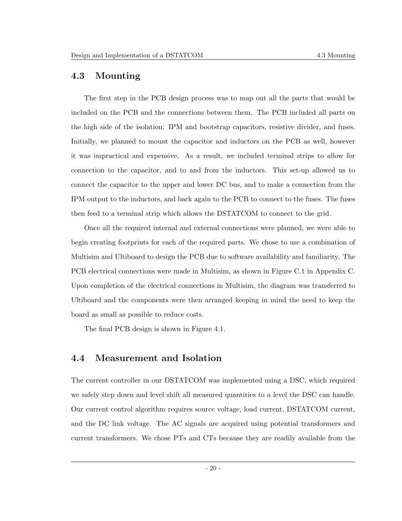
The AC signals being measured were converted to a bipolar voltage ranging between
±6V and ±8V. The ADC module for our DSC accepts inputs which are between 0 and 3.6V.
This meant that a signal conditioning circuit had to be designed to adjust the measured
signals for voltage and current to a 0-3.6V range. Figure 4.2 shows the schematic of the
signal conditioning circuit used for the measured voltage; the -5V DC offset was obtained
via LM337 negative voltage regulators, and LM741 operational amplifiers were the op-amps
- 21 -
Design and Implementation of a DSTATCOM 4.5 Protection
Fig. 4.2: Potential signal conditioning circuit
of choice.
We also had to measure the DC link capacitor voltage. This was done using a simple
resistive voltage divider which stepped down the maximum expected DC link capacitor
voltage (500V) to 2V. A 2.7MΩ resistor and 10kΩ resistor were used to implement the
voltage divider. Large resistors were chosen in order to keep the voltage divider from acting
as a discharge path for the capacitor. The voltage divider was isolated from the DSC by a
precision optically isolated voltage sensor. The ACPL-C87A was used for this because it is
specifically made to provide isolation for DC bus voltage sensing in VSC applications.
4.5 Protection
A considerable amount of time was put into making sure that there were sufficient safety
measures in place to protect both equipment and people working around the DSTATCOM.
Fortunately, Lab-Volt equipment comes with its own independent protection mechanisms
in place. Our source is 208VLL with an internal circuit breaker rated for 5A. The Lab-Volt
3-phase induction machine is also circuit breaker protected, eliminating the need for us to
- 22 -
Design and Implementation of a DSTATCOM 4.5 Protection
provide such protection.
The DSTATCOM is connected in shunt with the Lab-Volt equipment via time de-
lay/slow blow fuses rated for 3.15A. We put the fuses in place to protect the inductors
which are rated for 3A. Time delay/slow blow fuses were used to prevent the fuses from
blowing during transients lasting a few cycles.
In addition to using the fuses, we also made sure there was sufficient isolation between
the high voltage components of our system and the low voltage components. The PWM
outputs of the DSC were isolated from the IPM by digital isolators. Digital isolators, unlike
opto-isolators are transformer coupled; we chose digital isolators over opto-isolators because
they are twice as fast as opto-isolators, use less power, and have no extra cost associated
[11].
A power resistor connected in shunt with the DC link capacitor was also used as a
protection mechanism. It was put in place to make sure that we can safely discharge the
capacitor after turning off the DSTATCOM.
- 23 -

Design and Implementation of a DSTATCOM 5. Software
Chapter 5
Software
5.1 Introduction
One limitation of hardware components is the difficulty of initiating complex mathematical
functions. As such, software components (mainly microcontrollers) were used to perform
the mathematical functions required to run the decoupled current control algorithm. For
our application, the components running software algorithms must be capable of executing
trigonometric functions, performing Analog-to-Digital Conversions (ADC), running basic
control algorithms (such as PI controllers), as well as outputting data in a pulse-width
modulating format.
5.2 Digital Signal Controller
There are many varieties of microcontrollers on the market; those that simply perform
basic control functionality and others whose primary use is for advanced applications such
as power factor correction. In our application we decided to choose the controller which
best suited our design, a Digital Signal Controller (DSC).
- 24 -
Design and Implementation of a DSTATCOM 5.2 Digital Signal Controller
Our particular DSC is Microchip Technology Inc.’s dsPIC series chip, specifically the
dsPIC33F16GS402. It runs on a 40MHz external crystal oscillator, supports high speed
ADC, PWM, as well as integrated PI controller functions. By using these digital signal
processing libraries, we can save computation time over a standard MCU which increases
the quality of the output.
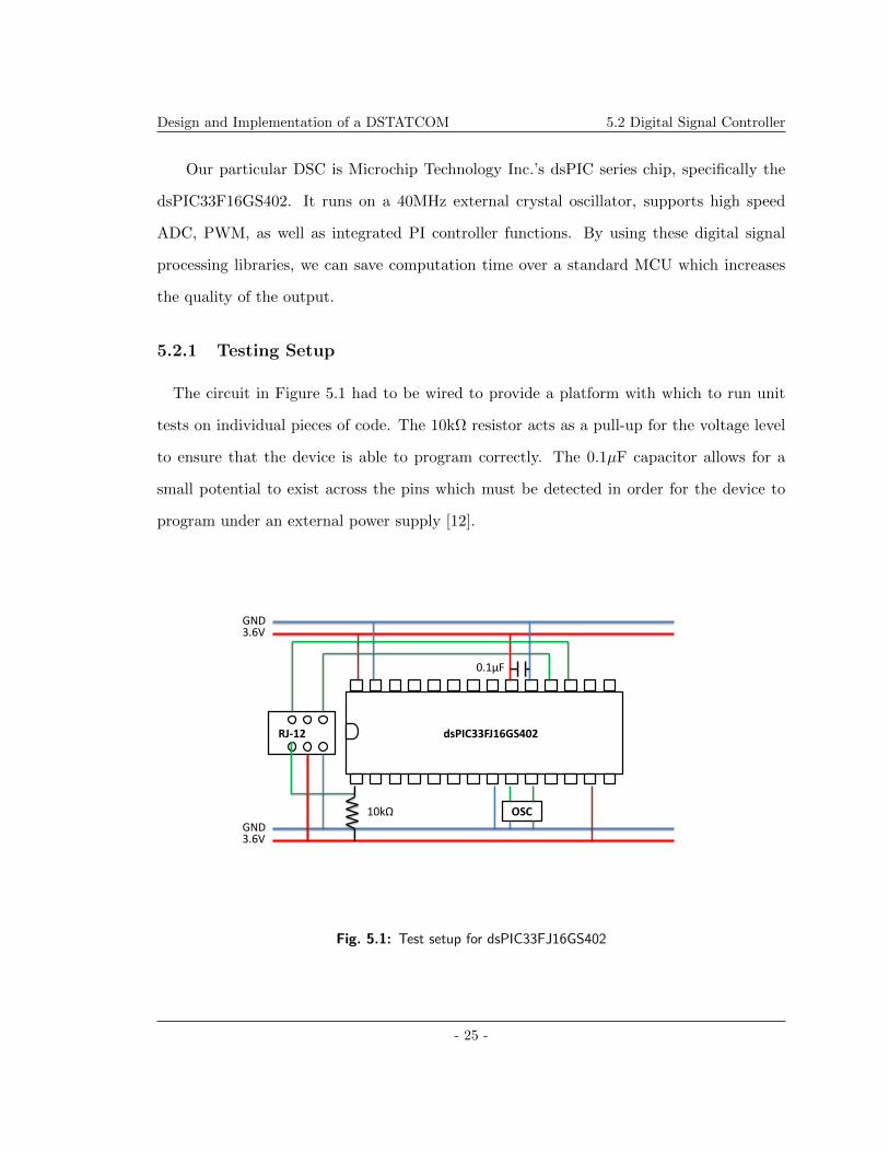
5.2.1 Testing Setup
The circuit in Figure 5.1 had to be wired to provide a platform with which to run unit
tests on individual pieces of code. The 10kΩ resistor acts as a pull-up for the voltage level
to ensure that the device is able to program correctly. The 0.1µF capacitor allows for a
small potential to exist across the pins which must be detected in order for the device to
program under an external power supply [12].
dsPIC33FJ16GS402
GND
GND
3.6V
3.6V
RJ-12
OSC 10kΩ
0.1μF
Fig. 5.1: Test setup for dsPIC33FJ16GS402
- 25 -

Design and Implementation of a DSTATCOM 5.3 Algorithms
5.3 Algorithms
The software components of this project are tasked with performing many mathematical
functions, as well as the input-output actions that are required to accomplish them. When
compiling the list of algorithms, we kept in mind the idea of modularity in that all systems
should have the ability to perform an individual unit test for functionality without requiring
the use of other source code. This ensured that should an individual encounter a problem
with one section of code it could be isolated from the rest of the program and debugged until
it operated as intended. The complete list of required algorithms with a brief description
of each is shown in Table 5.1. The following sections will outline the operation of each
algorithm in more detail, as well as any auxiliary software necessary to run the platform.
- 26 -

Design and Implementation of a DSTATCOM 5.3 Algorithms
Table 5.1: Algorithms
Algorithm Description
Data Acquisition Samples input waveforms scaled to a maximum value of 3.6Vand converts to a digital format to be handled by a conver-sion factor.
PLL Provides ramp output locked to the peaks of phase A sourcevoltage.
Forward Park Transform Generates 3-phase sinusoidal data from the PLL input andvarious sinusoid data and computes the Park’s transforma-tion to produce d and q quantities for use in the controlloop.
PI Control Executes a PI controller function complete with anti-windupfunctionality to limit the value of output within physicallimitations.
Control Loop Uses calculated values and PI Control to execute the mathe-matical operation required for the decoupled current control.
Inverse Park Transform Uses output from the Control Loop to compute the inversePark’s transformation on the data to generate sinusoidaldata.
PWM Compares sinusoidal data to a known threshold to generatea sinusoidally varying duty cycle which is given to a con-trol register to update the high-speed PWM module on thedsPIC.
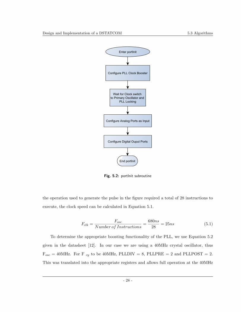
5.3.1 Initialization
Before the program can run, the DSC needs to run an initialization program to boost its
clock speed to the maximum of 40MHz, as well as configure the General Purpose Input
Output (GPIO) pins to analog or digital output. As per the data sheet, all pins that are
not in use by the program are set to be digital outputs so as not to interfere with the
operation of any of the pins in use. Figure 5.2 shows the flowchart of the portInit code
which is responsible for the operations discussed above.
The portInit routine was used in the first unit test to determine if the device was
operating at the correct clock speed. The results of the test are shown in Figure 5.3. Since
- 27 -
Design and Implementation of a DSTATCOM 5.3 Algorithms
Fig. 5.2: portInit subroutine
the operation used to generate the pulse in the figure required a total of 28 instructions to
execute, the clock speed can be calculated in Equation 5.1.
Fclk =Fosc
Number of Instructions=
680ns
28= 25ns (5.1)
To determine the appropriate boosting functionality of the PLL, we use Equation 5.2
given in the datasheet [12]. In our case we are using a 40MHz crystal oscillator, thus
Fosc = 40MHz. For F cy to be 40MHz, PLLDIV = 8, PLLPRE = 2 and PLLPOST = 2.
This was translated into the appropriate registers and allows full operation at the 40MHz
- 28 -
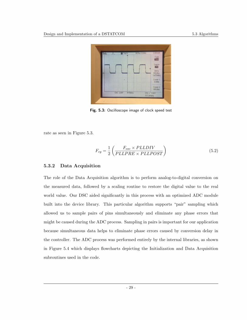
Design and Implementation of a DSTATCOM 5.3 Algorithms
Fig. 5.3: Oscilloscope image of clock speed test
rate as seen in Figure 5.3.
Fcy =1
2
(Fosc × PLLDIV
PLLPRE × PLLPOST
)(5.2)
5.3.2 Data Acquisition
The role of the Data Acquisition algorithm is to perform analog-to-digital conversion on
the measured data, followed by a scaling routine to restore the digital value to the real
world value. Our DSC aided significantly in this process with an optimized ADC module
built into the device library. This particular algorithm supports “pair” sampling which
allowed us to sample pairs of pins simultaneously and eliminate any phase errors that
might be caused during the ADC process. Sampling in pairs is important for our application
because simultaneous data helps to eliminate phase errors caused by conversion delay in
the controller. The ADC process was performed entirely by the internal libraries, as shown
in Figure 5.4 which displays flowcharts depicting the Initialization and Data Acquisition
subroutines used in the code.
- 29 -
Design and Implementation of a DSTATCOM 5.3 Algorithms
Fig. 5.4: Flowcharts for ADCInit (left) and Data Acquisition Subroutine (right)
The fractional data form allowed the conversion to output a value between 0 and 65575,
the maximum value for an unsigned integer. By using this very large range, we could then
scale the value down and eliminate any subtle errors that might have occurred in the ADC
process, since it can be affected by even the smallest disturbance in voltage. In order to
configure the registers properly, Microchip Technology Inc. provides a reference manual for
each built-in module on its DSCs. This document proved vital in achieving proper operation
of the ADC module and allowed for the most accurate results [13].
The scaling portion of this routine allowed for us to use the real world values of the volt-
age and current measurements in our control algorithm. When we scale to the appropriate
values, we can then use our simulation results to calibrate the control algorithm to match
what we would expect as an output, which helped with the debugging process. Equation 5.3
shows how the scaling was performed.
- 30 -

Design and Implementation of a DSTATCOM 5.3 Algorithms
Xscaled = X × MaxV alue
32787−MaxV alue (5.3)
where X is the discrete converter value (between 0-65575) and Xscaled is the real world
equivalent value. By using this equation, we can scale the digital value to a proportion
of its real world maximum, and then using the subtracted term, we zero the value. This
zeroing is only used for the sinusoidal data to allow for negative numbers to be used in the
control loop.
5.3.3 Park’s Transformations
The transformation algorithms serve the role of converting the data into the dq0 domain.
The algorithm is based off of an optimized version of the Park’s transformation given in
Equation 2.4. To optimize this equation we simply eliminate the number of occurrences of
trigonometric functions, since they are typically the slowest portion of code. This algorithm
first uses the results of the Data Acquisition program to obtain values for the magnitude of
system measurements, as well as the PLL locking angle for the system. Using the magnitude
and angle of phase A, it creates three-phase sinusoidal data from this information as the
pre-requisite for the Park’s transformation. Once these values are calculated, the d and q
components of the transform are generated for use in the Control Loop.
One goal when developing this algorithm was to eliminate the repetitive use of trigono-
metric functions, as well as optimize the number of calculations required. Trigonometric
functions are very slow to calculate, even with an approximation, and repetitive calcula-
tions waste both memory and processing power. Thus, temporary variables were assigned
which contain the calculated trigonometric values, and sections of the transformation were
eliminated that were unnecessary. In our case, we do not calculate the value of the 0 com-
ponent of the transformation because it is unused and always results in a value of 0 for our
balanced load scenario. By making these modifications we were able to increase the speed
- 31 -

Design and Implementation of a DSTATCOM 5.3 Algorithms
of our program by over 250% from the original run time.
In order to test these algorithms, we used an equivalent section of code in MATLAB to
generate the expected result. We used MATLAB because it was much simpler to generate
sinusoidal test signals in the software than in our C code. After the MATLAB test we were
able to generate the plot shown in Figure 5.5.
Fig. 5.5: d and q components of Park’s transformation in MATLAB
Figure 5.5 shows that our code generates a d-axis locking to the magnitude of the
voltage, and a q-axis with a value of zero which we expect. We then applied the sample
test signal data to our C code and were able to replicate this result exactly.
Similarly to the forward transformation, the inverse transform was tested in MATLAB.
The goal was to reconstruct the sinusoidal data in three phases based on the d and q
components generated by the first algorithm. Figure 5.6 shows the results; the sinusoidal
data was successfully reconstructed from the d and q components of the forward transform.
5.3.4 PI Control
The PI controller algorithm is governed by the standard equation given in Equation 5.4.
For our discrete case, the integral is approximated by Equation 5.5.
- 32 -

Design and Implementation of a DSTATCOM 5.3 Algorithms
Fig. 5.6: Three-phase components of inverse transformation in MATLAB
u(t) = Kp × e(t) +Ki ×∫ b
ae(t) dx (5.4)
Integral = PreviousIntegral + Error × dt (5.5)
Integral is the sum of all previous values of the integral calculation, Error is the input
to the controller, dt is the time step from the previous instigation of the function, Kp and
Ki are the gains of the controller, and u(t) is the overall output back to the system. This
function uses the trapezoidal method of discrete integration given in Equation 5.6.
C =
(A+B
2
)∗ dt (5.6)
- 33 -

Design and Implementation of a DSTATCOM 5.3 Algorithms
where C is the area, and A and B are points along the curve. The time step is so small
in our case that A and B can be approximated as the same value thus we see the result in
Equation 5.5. Figure 5.7 shows the response of the digitally implemented PI controller to
a step input against a pre-fabricated PI controller tuned using MATLAB-Simulink. Both
are controlling an identical second-order plant.
Fig. 5.7: PI Response to a step input
As can be seen from the figure, the response of the digital controller is not as smooth
as the continuous, however, with precise tuning parameters the value and response can be
tuned as finely as the continuous. These results are satisfactory for the performance that
we expect out of our design and suffice for the purpose of this project.
5.3.5 Pulse-Width Modulation
Sinusoidal pulse-width modulation is a method used to control the switching of the IPM
in the VSC. In our system, we compare the 60Hz, 3-phase sinusoidal voltage output of the
control algorithm to a 15kHz triangular waveform to yield the train of pulses required to
produce a 60Hz sinusoidal waveform at the output of the VSC.
- 34 -

Design and Implementation of a DSTATCOM 5.3 Algorithms
The PWM module of the DSC was a built-in function. The bulk of the work lied in
enabling the appropriate control registers and configuring them such that the output of the
module yields six pulse trains to drive the IPM. A flowchart of the configuration of the
module is given in Figure 5.8.
Fig. 5.8: SPWM module configuration
The duty cycle of the SPWM outputs were varied sinusoidally to produce a sinusoidally
varying output of 60Hz. This was accomplished by updating the PWM duty cycle register.
Unit tests of the SPWM module were performed by varying the duty cycle and observing
the output. The input sinusoidal waveform is shown in Figure 5.9, overlaid with the resulting
SPWM pulses produced by the DSC. The modulation index for this wave is 1 utilizing the
full range on voltage input on the DSC.
To aid in the design of the capacitor pre-charging circuit, we had to establish the logic
of the SPWM output pulses that would be fed to the IPM. Table 5.2 shows a simplified
truth table extracted from the IPM datasheet [1].
From Table 5.2, it was necessary for the DSC to feed to the IPM the exact same signal
to each pair of complementary switches. The existence of the NOT gate was later proved
- 35 -

Design and Implementation of a DSTATCOM 5.3 Algorithms
Fig. 5.9: Unit test for PWM
Table 5.2: Simplified truth table of IGBT switch vs. PWM input state [1]
Signal to Low Signal to High Low Switch High Switch
H L Open Open
L L Closed Open
H H Closed Open
by the application guide [10].
5.3.6 Phase-Locked Loop
A phase-locked loop (PLL) is used to extract the fundamental frequency and phase
information of an input signal. It is very important to accurately determine the phase
angle, θ, of our source voltage in order for the Park’s transformation to align to the proper
axis.
Many of the difficulties associated with implementing a PLL lie with unbalanced con-
ditions, faults, and harmonics in the voltage [14]. The Lab-Volt source voltage has limited
- 36 -

Design and Implementation of a DSTATCOM 5.3 Algorithms
distortion that would normally be caused by faults, non-linearities, or changes in the grid
load conditions. For this reason, we considered the source voltage to be a strong 60Hz
voltage.
The most widely implemented PLL method is the Synchronous Reference Frame PLL
(SRF-PLL) and is described in detail in [15]. This method handles distorted conditions and
is very adept in terms of handling transients. However, due to the voltage source we used,
we decided to implement a simpler PLL which employs a Zero-Crossing Detector (ZCD).
The ZCD detects the positive transition zero crossing of the voltage and outputs a
square pulse. The time between each pulse is 16.67ms - the period of a 60Hz signal. The
ZCD of the PLL was implemented in hardware and the circuit schematic is shown in Figure
5.10.
Fig. 5.10: ZCD circuit schematic
The input of the ZCD is the scaled source voltage which varies from 0-3.6V; the actual
zero of this voltage is 1.8V. The first stage outputs a square pulse at every crossing of
1.8V. This is level shifted and attenuated in the second stage to output a pulse with a
- 37 -

Design and Implementation of a DSTATCOM 5.3 Algorithms
magnitude of 3.6V. The pulse is sent to the DSC executing the PLL algorithm to indicate
a zero crossing, and to begin calculating θ.
The phase angle, θ, is calculated in software and is given by the equation:
θ = 2πft (5.7)
As time progresses, θ varies linearly from to 0 to 360 . The output of the PLL in PSCAD
with the source voltage is shown in Figure 5.11. Note that the PLL locks to the peaks of
the voltage.
Fig. 5.11: PLL in PSCAD
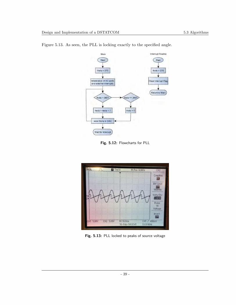
This ramp output was implemented in software, and the flowchart is shown in Figure
5.12. This algorithm monitors the output of the ZCD and also calculates θ continuously. To
avoid affecting the speed of the overall control algorithm, we implemented the calculation
of θ on a second DSC.
The positive edge of the ZCD pulse is detected and triggers the calculation of θ. Since
we require locking to the peaks of the voltage, θ must be initially 270 . The digital value
of θ is converted to an analog value between 0 and 3.6V using a DAC8562 chip, and is then
fed to the main DSC performing the control loop calculations.
A locking angle of 90 was configured, and the results of the final unit test is shown in
- 38 -
Design and Implementation of a DSTATCOM 5.3 Algorithms
Figure 5.13. As seen, the PLL is locking exactly to the specified angle.
Fig. 5.12: Flowcharts for PLL
Fig. 5.13: PLL locked to peaks of source voltage
- 39 -

Design and Implementation of a DSTATCOM 5.4 Conclusion
5.4 Conclusion
From the description of the algorithms we can see that after extensive testing of the individ-
ual subroutines, the algorithms were fully functional before being connected to the hardware
designs. After the testing was completed, the DSC units as well as the required DAC were
mounted on a soldering board for convenience and assurance of connection. The overall
implementation and connection to external peripheral measurements will be discussed in
Chapter 6.
- 40 -

Design and Implementation of a DSTATCOM 6. Implementation
Chapter 6
Implementation
6.1 Intelligent Power Module Set-up
Upon completion of the Hardware and Software designs, we commenced with interfacing of
the individual components of our system. In order to accomplish this with minimal error
we employed a modular test plan to accommodate integration of all parts of the system.
The test plan can be found in Appendix A.
At the final step of the test plan, we encountered problems integrating the IPM with the
rest of the components on the PCB, as well as the capacitor. The system was experiencing
a short-circuit scenario while attempting to perform a battery charge on the capacitor.
After extensive troubleshooting it was discovered that the IPM we had chosen was drawing
an extraordinary amount of current while attempting to charge the capacitor, effectively
overloading the Lab-Volt source. To rectify the error in the system, we decided to bypass
the IPM entirely in favour of the Lab-Volt IGBT Chopper/Inverter Module.
After bypassing the IPM we were able to perform a successful system charge of the
capacitor through the flyback diodes in the Inverter module. Following this success we were
able to achieve SPWM outputs using firing pulses generated by our DSC. The results can
- 41 -
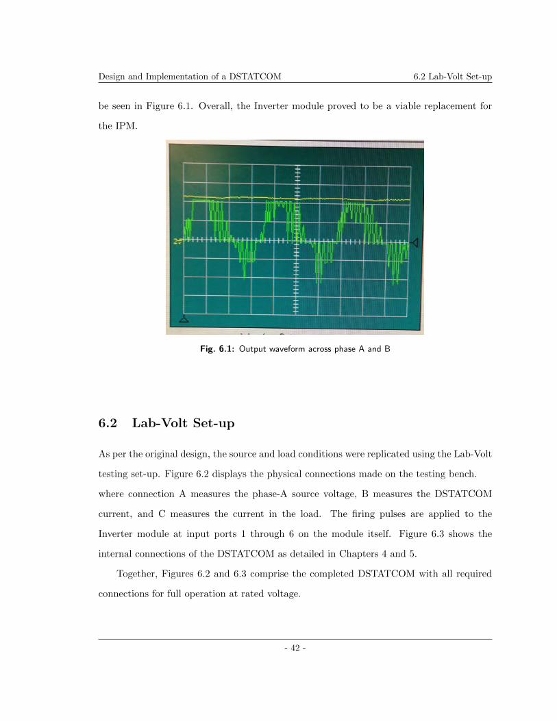
Design and Implementation of a DSTATCOM 6.2 Lab-Volt Set-up
be seen in Figure 6.1. Overall, the Inverter module proved to be a viable replacement for
the IPM.
Fig. 6.1: Output waveform across phase A and B
6.2 Lab-Volt Set-up
As per the original design, the source and load conditions were replicated using the Lab-Volt
testing set-up. Figure 6.2 displays the physical connections made on the testing bench.
where connection A measures the phase-A source voltage, B measures the DSTATCOM
current, and C measures the current in the load. The firing pulses are applied to the
Inverter module at input ports 1 through 6 on the module itself. Figure 6.3 shows the
internal connections of the DSTATCOM as detailed in Chapters 4 and 5.
Together, Figures 6.2 and 6.3 comprise the completed DSTATCOM with all required
connections for full operation at rated voltage.
- 42 -

Design and Implementation of a DSTATCOM 6.2 Lab-Volt Set-up
Fig. 6.2: Lab-Volt test set-up; A: phase-A source voltage, B: DSTATCOM current mea-surement, C: load current measurement
Fig. 6.3: Hardware Configuration: a) Signal Conditioning circuits; b) DSC; c) MeasurementBoard; d) PCB and Control connections e) Inductors f) Capacitor and discharge switch
- 43 -

Design and Implementation of a DSTATCOM 6.3 Results
6.3 Results
We used a modular method of connecting the system which revealed positive results in
multiple areas of the system. After connecting the measurements to the signal condition-
ing, we were able to view the scaled and shifted output waveform from the circuit which
indicated that the measurements and inputs to the DSC would be acceptable. Following
this confirmation we were able to replicate a sine wave similarly to the unit test shown in
Figure 5.9. Using these inputs to the system we were able to replicate the unit test displayed
in Figure 6.1 which confirmed that the voltage would charge the capacitor to an acceptable
level.
Unfortunately due to unforeseen circumstances, we were not able to achieve the goal
of power factor correction and full system integration. Details on the continuation of work
can be found in Chapter 7.
- 44 -

Design and Implementation of a DSTATCOM 7. Conclusions
Chapter 7
Conclusions
This report has detailed the design and implementation of a DSTATCOM for power factor
correction for the ECE4600 Group Design Project. The DSTATCOM is a solid-state device
employing power electronic switches to achieve flexible reactive power injection at the load
end of a transmission system. Our system uses IGBT-based power electronics in a 6-pulse
inverter configuration, controlled through the use of a decoupled instantaneous current
controller. The system allows for completely independent control of both active and reactive
power within the system, enabling full power factor correction.
7.1 Future Work
The remaining portion of the project includes testing the system as a whole and verifying
the operation as compared to simulated results.
The control algorithm implemented in this project has the added ability to correct for
voltage sag in a separate mode outside of power factor correction. This would required
extra time to develop an AC current control loop and implement a function to perform this
task in the DSC. Full functionality with both operating modes included would be an added
benefit to the system. This would require additional hardware and measurements as well
- 45 -

Design and Implementation of a DSTATCOM 7.1 Future Work
as external controls for switching operating modes at the will of the human controller.
Additionally, we could continue to develop the hardware of the system to a full embed-
ded state including a functional IPM outside of the Lab-Volt testing set-up. Included with
this would be minimizing the space required to operate the device, as well as beautifying
the components with minimal external power sources and connections. This would allow
for integration with low-voltage loads outside of a lab environment.
- 46 -
Design and Implementation of a DSTATCOM REFERENCES
References
[1] SLLIMM small low-loss intelligent molded module IPM, Datasheet, STMicroelectron-ics, Mar. 2008.
[2] S. D.Masand and G. Agnihotri, “Distribution Static Compensator Performance UnderLinear and Nonlinear Current Regulation Methods,” Journal of Electrical Systems,vol. 4, pp. 91–105, 2008.
[3] J. Arrillaga, Flexible Power Transmission – the HVDC Options. John Wiley and SonsLtd, 2007.
[4] B. S. Ambarnath Banerji, Sujit K. Biswas, “DSTATCOM Control Algorithms: A Re-view,” International Journal of Power Electronics and Drive Systems, vol. 2, pp. 285–296, 2012.
[5] S. K. Sethy, “Design and Simulation of Current and Voltage Linear Controller of aSTATCOM for Reactive Power Compensation Using Variation of DC Link Voltage,”International Journal of Computing and Applied Science, vol. 1, pp. 50–65, 2013.
[6] K. K. Pinapatruni and K. M. L, “DQ based control of DSTATCOM for Power QualityImprovement,” VSRD International Journal of Electrical, Electronics & Communica-tion Engineering, vol. 2, pp. 207–227, May 2012.
[7] E. Acha, V. Agelidis, O. Anaya, T.J.E. Miller, Power Electronic Control in ElectricalSystems. Oxford, Boston: Newness, 2002.
[8] O. A. T. M. Enrique Acha, Vassilios Agelidis, Power Electronic Control in ElectricalSystems. Woburn,MA USA,: Butterworth-Heinemann Publishing House.
[9] B. Kanchanapalli and M. Valavala, “Design and Simulation of Current and VoltageLinear Controller of a STATCOM for Reactive Power Compensation Using Variationof DC Link Voltage,” International Journal of Computing and Applied Science, vol. 1,pp. 47–51, 2012.
[10] AN3338 Application Note SLLIMM small low-loss intelligent molded module, Applica-tion Guide, STMicroelectronics, Sep. 2012.
- 47 -

Design and Implementation of a DSTATCOM REFERENCES
[11] When to Use Digital Isolators vs. Optocouplers, Silicon Labs, 2009.
[12] dsPIC33FJ06GS101/X02 and dsPIC33FJ16GSX02/X04, Microchip Technology Inc.,2008-2012. [Online]. Available: http://ww1.microchip.com/downloads/en/DeviceDoc/70318F.pdf
[13] Section 16. Analog-to-Digital Converter (ADC), Microchip Technology Inc., 2006-2012.[Online]. Available: ww1.microchip.com/downloads/en/DeviceDoc/70183D.pdf
[14] M. L. F. Blaabjerg, R. Teodorescu and A. Timbus, “Overview of Control and GridSynchronization for Distributed Power Generation Systems,” IEEE Transactions onIndustrial Electronics, vol. 53, pp. 1398–1409, 2006.
[15] F. Xiong, W. Yue, L. Ming, W. Ke, and L. Wanjun, “A Novel PLL for Grid Syn-chronization of Power Electronic Converters in Unbalanced and Variable-FrequencyEnvironment,” 2nd IEEE International Symposium on PEDG, 2010.
- 48 -

Design and Implementation of a DSTATCOM A. Project Notes
Appendix A
Project Notes
Table A.1: Original specifications (set 2014-09-27)
Description Requirement
Source Voltage 3-phase 173VLLLoad 3-phase variable
Total Harmonic Distortion (THD) < 5%
Maximum VAR compensation 1kVAr
Power Factor 1
The project test plan is shown on the following pages.
- 49 -

PART 1 INTRODUCTION
1.1 OBJECTIVE
The purpose of this document is to provide a methodological way of building our DSTATCOM. Please follow the document to the letter, lots of thought was put into it and effort to write it. If you think something is wrong please feel free to bring it up.

TESTS
1.1 DIGITAL ISOLATORS ACCEPTANCE TEST
Test Description and Procedure
Test ID 001
Test Description
The purpose of the test is to verify the functionality of the digital isolators on the PCB
Acceptance Criteria
On the oscilloscope you should be able to see identical PWM pulses at pins In1 and Out1 of the
digital isolators.
Preparation 1. Make sure nothing is connected to the PCB.
2. Solder the three digital isolators on to the PCB.
3. Connect the two 5 volts power supplies and grounds needed by the digital isolators. There
shouldn’t be any other component or power supply other than what is needed by the
digital isolators.
Test Procedure
1. Configure the DSC to output PWM pulses with a duty cycle of 50% and switching frequency
of 1 kHz.
2. Check on the oscilloscope that the pulses are at 1 kHz.
3. Turn on the power supplies for the digital isolators and using a multi-meter to make sure
that the voltage between Vd1 and Gnd1 is 5V and the same for voltage between Vd2 and
Gnd2.
4. Turn off the power supplies.
5. Connect the PWM pulses of the DSC to the terminal strips on the PCB.
6. Connect channel 1 and channel 2 on the oscilloscope e to In1 and Out2 on the digital
isolators.
7. Turn on the power supplies and click auto set on oscilloscope.
8. Observe the waveforms.
9. Repeat procedure 6-7 for all the digital isolators.
Note: Expected result is identical PWM pulses without any attenuation or noise in Out2.
Results
Test ID 001 Test Name Digital Isolators Result (Pass/Fail)
Tested by Initials & Date
Observations

1.2 CAPACITOR CHARGING
Test Description and Procedure
Test ID 002
Test Description
The purpose of the test is to verify that we can charge the capacitor when it is connected to the
PCB board.
Acceptance Criteria
1. Successfully charge the capacitor.
2. Check to make sure digital isolators still functioning properly.
Note : Both must pass for advancement to the next stage.
Preparation 1. Connect the capacitor to labvolt DC source and the PCB.
Test Procedure
1. Open Lab volt software on the workbench and make sure that the meters which show
measurements are turned on.
2. Charge the capacitor to 20V and then turn off the DC source on lab volt without
disconnecting anything.
3. With the DC source turned off the meters in the Lab volt software must show the DC voltage
slowly discharging. This means our capacitor has successfully been charged.
4. Connect the PWM pulses of the DSC to the terminal strips on the PCB.
5. Connect channel 1 and channel 2 on the oscilloscope e to In1 and Out2 on the digital
isolators.
6. Turn on the power supplies and click auto set on oscilloscope.
7. Observe the waveforms. You should observe the same waveforms as in test 1.1.
Note : Do not disconnect the capacitor, it will be needed for the next test.
Results
Test ID 002 Test Name CAPACITOR CHARGING Result (Pass/Fail)
Tested by Initials & Date
Observations
1.3 ISOLATED VOLTAGE SENSOR
Test Description and Procedure
Test ID 003

Test Description
The purpose of the test is to verify the functionality of the Avago isolated voltage sensor.
Acceptance Criteria
We should measure the stepped down voltage at the outputs of isolated voltage sensor. That is
the voltage across Vout+ and Vout-.
Preparation 1. Solder the Avago isolated voltage sensor on the PCB and all its peripherals i.e voltage divider
and capacitors it needs.
2. Turn on the 5V power supplies and using a multi-meter measure the voltage between VDD1
and GND1 and the same for VDD2 and GND2. It should be 5V for both.
Test Procedure
1. Open Lab volt software on the workbench and make sure that the meters which show
measurements are turned on.
2. Charge the capacitor to 40V and then turn off the DC source on lab volt without
disconnecting anything.
3. On the terminal strips for Vout+ and Vout- connect a multi-meter.
4. The multi-meter should ~0.15V and that should slowly drop at the capacitor discharges.
5. Connect the PWM pulses of the DSC to the terminal strips on the PCB. This is after capacitor
has fully discharged.
6. Connect channel 1 and channel 2 on the oscilloscope to In1 and Out2 on the digital isolators.
7. Observe the waveforms. You should observe the same waveforms as in test 1.1.
Results
Test ID 003 Test Name Isolated voltage sensor Result (Pass/Fail)
Tested by Initials & Date
Observations
1.4 IGBT BRIDGE
Test Description and Procedure
Test ID 004
Test Description
To determine the functionality of the IGBT bridge.
Acceptance Criteria
1. Observe a sine wave at the output of the VSC
2. Measure the voltage across the bootstrap capacitor.
Preparation 1. Put the heat sink on the IGBT Bridge.
2. Solder the IGBT bridge to the PCB
3. Get 1uF capacitors from the techshop and also solder them on as the bootstrap capacitors.
4. Pin Cin should be connected to 0V which l assume is ground. This will have the smart
shutdown function disable because the comparator will always output zero.

5. Connect the power supplies for the IGBT and turn them on.
6. Measure the bootstrap voltage across the capacitor. It should be in the range of Vcc.
Test Procedure
1. Check on the oscilloscope again that the PWM outputs of the DSC are at 1 kHz.
2. Connect the outputs of the IGBT Bridge at the terminal strips to the oscilloscope.
3. Charge the capacitor to 20V and verify using the lab volt software on the computer.
4. Connect the PWM outputs of the DSC to the terminal strips of the PCB.
5. Click auto set on oscilloscope and observe the waveform. You should see something like this
Results
Test ID 004 Test Name IGBT Bridge Result (Pass/Fail)
Tested by Initials & Date
Observations
TESTS
1.1 SIGNAL CONDITIONING
Test Description and Procedure
Test ID 001
Test Description
The purpose of this test is to determine to see if our signal conditioning circuit will work under
normal operating conditions i.e. if we are running a motor and changing its speed.
Acceptance Criteria
The output of the signal conditioning circuit follows changes in the grid and doesn’t go below 0V
and above 3.6V.
The output of the signal conditioning circuit mustn’t show any saturation.
Preparation 1. Connect the labvolt equipment to the three phase induction motor and make sure it is
running properly.
2. Turn it off and make sure that everything is de-energized.
3. Connect the measuring board to measure the source voltage and current.
4. Connect the signal conditioning circuit to the output of the measuring board.
5. Connect an oscilliscope to the outputs of signal conditioning circuit.
Test Procedure
1. Run the motor and change its speed whilst monitoring the outputs of the signal
conditioning.
2. Monitor the output of the signal conditioning and observe the results.
Results
Test ID 001 Test Name Signal Conditioning Result (Pass/Fail)
Tested by Initials & Date
Observations
1.2 PLL
Test Description and Procedure
Test ID 002
Test Description
The purpose of the test is to verify that we are locking to the peaks of the source voltage.
Acceptance Criteria
Lock to the peaks of the source voltage.
Preparation 1. Keep the connection as above
2. Connect output of DAC and the source voltage to the oscilliscope
Test 1. Run the motor at different speeds and also vary the source voltage.
Procedure 2. Observe the results.
Results
Test ID 002 Test Name PLL Result (Pass/Fail)
Tested by Initials & Date
Observations
1.3 DC CAPACITOR CHARGING
Test Description and Procedure
Test ID 003
Test Description
The purpose of the test is to verify that we can charge capacitor to 200V and also measure its
voltage via the resistive voltage divider. The capacitor will be charged via diode rectification.
Acceptance Criteria
We should measure the stepped down voltage at the outputs of isolated voltage sensor. That is
the voltage across Vout+ and Vout-.
Preparation 1. Connect the output of the oscilloscope.
2. Connect the outputs of the signal conditioning circuit to the oscilloscope.
3. It is important to keep the previous connection as it is. The motor should still be connected
as well as the signal conditioning circuit.
Test Procedure
1. Run the motor and charge the capacitor. We should see the measured voltage on the DC
link capacitor go up. About 0.75V.
Results
Test ID 003 Test Name DC Capacitor Charging Result (Pass/Fail)
Tested by Initials & Date
Observations
1.4 PWM TEST
Test Description and Procedure
Test ID
Test Description
Acceptance Criteria
Get it working with DC
Preparation
Results
Test ID 004 Test Name IGBT Bridge Result (Pass/Fail)
Tested by Initials & Date
Observations

Design and Implementation of a DSTATCOM B. Budget Summary
Appendix B
Budget Summary
The following page shows our budget summary. After consultation with our advisor, wewere provided with funds beyond our original $400 budget. Group members also contributed$120 of the $809.86 listed; this brings the amount donated by the ECE Department toapproximately $690.
- 58 -

Item(s) Part Number Supplier Qty Unit CostTotal
Cost
28 I/O DSC DSPIC33EP64MC502-I/SS Digikey 3 $5.00 $15.00
28 I/O DSC THC DSPIC33FJ16GS402 Mouser 2 $4.79 $9.58
28 I/O DSC THC DSPIC33FJ16GS402 Digikey 2 $5.02 $10.04
Intelligent Power Module STGIPS20C60 Mouser 2 $25.00 $50.00
PCB Board - Alberta Printed Circuits 2 - $294.00
Variable power supply LM317KCT Mouser 4 $0.69 $2.76
5V Power supply L7805CV-DG Mouser 4 $0.63 $2.52
Digital isolators HCPL-9030-000E Mouser 9 $7.70 $69.30
Isolated voltage sensor ACPL-C87A-000E Mouser 3 $7.39 $22.17
2200 uF Capacitor ALS30A222NP500 Mouser 1 $69.09 $69.09
2.7Mohm Resistor 294-2.7M-RC Mouser 4 $0.34 $1.36
10kohm Resistor 294-10K-RC Mouser 5 $0.34 $1.70
Capacitor 100pF SR151A101JAR Mouser 6 $0.33 $1.99
Capacitor 1uF ECA-2WM010 Mouser 9 $0.50 $4.54
Capacitor 0.11uF FK22X7R2J104K Mouser 5 $1.72 $8.60
Inductor 159ZE Mouser 3 31.71 $95.13
Fuses 04773.15MXP Mouser 9 $1.63 $14.67
Passive Components, Solder
Boards- ECE Tech Shop $0.00
12V Power Supply - Power Systems Group $0.00
15V Power Supply - Power Systems Group $0.00
PT/CT Measurement Board - Power Systems Group $0.00
Enclosure Box - Warren Lavallee $0.00
Lab-Volt Equipment Power Systems Group $0.00
$672.44
$50.00
$87.42
$809.86
Shipping & Brokerage
Taxes
Total
Subtotal

Design and Implementation of a DSTATCOM C. Figures
Appendix C
Figures
Fig. C.1: PCB electrical connections in Multisim
- 60 -
Recommended


![REVIEW OF CONTROL STRATEGIES OF DSTATCOM · Fig. 2 Equivalent circuit of DSTATCOM The operation of DSTATCOM is explained in the following modes [2]: Mode 1: If V SHabc is in-phase](https://img.pdfslide.net/doc/110x75/5ec37ced6f2e09596744a3b6/review-of-control-strategies-of-dstatcom-fig-2-equivalent-circuit-of-dstatcom-the.jpg)