Scholars' Mine Scholars' Mine
Masters Theses Student Theses and Dissertations
Summer 2016
Design of a microwave imaging system for rapid wideband Design of a microwave imaging system for rapid wideband
imaging imaging
Matthew Jared Horst
Follow this and additional works at: https://scholarsmine.mst.edu/masters_theses
Part of the Electrical and Computer Engineering Commons
Department: Department:
Recommended Citation Recommended Citation Horst, Matthew Jared, "Design of a microwave imaging system for rapid wideband imaging" (2016). Masters Theses. 7555. https://scholarsmine.mst.edu/masters_theses/7555
This thesis is brought to you by Scholars' Mine, a service of the Missouri S&T Library and Learning Resources. This work is protected by U. S. Copyright Law. Unauthorized use including reproduction for redistribution requires the permission of the copyright holder. For more information, please contact [email protected].

DESIGN OF A MICROWAVE IMAGING SYSTEM FOR RAPID WIDEBAND
IMAGING
By
MATTHEW JARED HORST
A THESIS
Presented to the Faculty of the Graduate School of the
MISSOURI UNIVERSITY OF SCIENCE AND TECHNOLOGY
In Partial Fulfillment of the Requirements of the Degree
MASTER OF SCIENCE IN ELECTRICAL ENGINEERING
2016
Approved by:
Dr. Reza Zoughi, Advisor
Dr. Mohammad Tayeb Ghasr
Dr. Randy H. Moss
Dr. Joe Stanley

2016
Matthew Jared Horst
All Rights Reserved

iii
ABSTRACT
An imaging system composed of two linear arrays of antennas is designed
through full-wave simulation and fabricated for use in synthetic aperture radar imaging.
The arrays electronically scan along their antenna elements and are mechanically moved
along a second orthogonal direction for scanning large two-dimensional areas quickly.
Each linear array is printed on a circuit board where the antenna elements are integrated
into the edge of the board as tapered slot-line antennas operating at 22 to 27 GHz. A
multiplexer circuit is printed onto each linear array to transmit wideband signals to each
antenna in the array. Receivers are printed onto the radiating end of the antennas on the
edge of the circuit board. These receivers are less complex than traditional microwave
receivers, and they require no phase calibration for synthetic aperture radar processing. A
controller board is designed and fabricated to facilitate electronic scanning along the
arrays and route measurement data to a PC for storage. The linear arrays and controller
board are mounted on a small mechanical scanning table for moving the arrays along one
direction. All receivers are calibrated for variations in voltage outputs among the
elements by scanning a known target and applying an equalization matrix. Several targets
are scanned by the final imaging system, and the resulting images show the ability of the
system to detect dielectric contrast under the surface of dielectric materials. The tapered
slot-line antenna is redesigned and improved for -10 dB reflection coefficient across the
operating frequency band and higher voltage output of the receivers with respect to the
original antenna design. Imaging results of the redesigned antenna show how
refabricating the imaging system with the improved antenna will improve overall image
quality of the system.

iv
ACKNOWLEDGMENTS
I would like to thank my advisor, Dr. Reza Zoughi, for encouraging me to pursue
a career in scientific research and development and providing me with the opportunity to
achieve a master’s degree at Missouri University of Science and Technology.
I would also like to thank Dr. Mohammad Tayeb Ghasr for his feedback and
guidance for all my research endeavors, including this investigation. Thank you to Dr.
Moss and Dr. Stanley for serving on my committee as well.
Thanks to the National Science Foundation for awarding me with the Graduate
Research Fellowship and supporting me through this project.
Thanks to Mr. Jeffrey Birt for machining the metal shields and scanning table
used in the imaging system.
Thanks to Mr. Matthew Dvorsky for providing me with the programming code
and teaching me embedded programming necessary for writing the software for the
imaging system. Thank you to all of my colleagues at the Applied Microwave Testing
Laboratory (amntl), both present and alumni, for your guidance and support.
Finally, I would like to thank my family and friends for their love and support.

v
TABLE OF CONTENTS
Page
ABSTRACT ....................................................................................................................... iii
ACKNOWLEDGMENTS ................................................................................................. iv
LIST OF ILLUSTRATIONS ............................................................................................ vii
LIST OF TABLES .............................................................................................................. x
SECTION
1. INTRODUCTION ...................................................................................................... 1
1.1. MICROWAVE AND MILLIMETER WAVE IMAGING ................................. 1
1.2. RECENT WORK ................................................................................................. 3
1.3. SCOPE AND GOAL ............................................................................................ 8
2. SYSTEM DESIGN ................................................................................................... 11
2.1. ANTENNA DESIGN ......................................................................................... 12
2.1.1. Design and Simulation. ............................................................................... 12
2.1.2. Physical Layout. .......................................................................................... 28
2.1.3. Antenna Measurement. ............................................................................... 30
2.2. ARRAY DESIGN .............................................................................................. 34
2.2.1. Signal Flow Design. .................................................................................... 34
2.2.2. Array Simulations. ...................................................................................... 38
2.2.3. Array Fabrication. ....................................................................................... 40
2.3. CONTROLLER BOARD .................................................................................. 41
3. SYSTEM TEST ........................................................................................................ 47
3.1. MEASUREMENT SETUP ................................................................................ 47
3.1.1. Scan Table. .................................................................................................. 47
3.1.2. Scanner Software. ....................................................................................... 49
3.1.3. Array Equalization. ..................................................................................... 50
3.1.4. Addition of a Second Linear Array. ............................................................ 53
3.2. IMAGING RESULTS ........................................................................................ 56
3.2.1. Foam with Rubber Inclusions. .................................................................... 56
3.2.2. Metal Keys. ................................................................................................. 58

vi
3.2.3. Rubber Sheet with Voids. ........................................................................... 59
3.2.4. Missouri “S&T” Logo................................................................................. 60
4. DESIGN OF AN IMPROVED ANTENNA ............................................................. 63
4.1. DESIGN AND SIMULATION .......................................................................... 63
4.2. PHYSICAL LAYOUT ....................................................................................... 86
4.3. ANTENNA MEASUREMENT ......................................................................... 87
5. SUMMARY .............................................................................................................. 93
6. FUTURE WORK ...................................................................................................... 94
APPENDICES
A. ORIGINAL ANTENNA DESIGN .......................................................................... 95
B. LINEAR ARRAY DESIGN .................................................................................. 101
C. CONTROLLER BOARD CIRCUIT MODELS .................................................... 112
D. IMPROVED ANTENNA DESIGN ....................................................................... 122
BIBLIOGRAPHY ........................................................................................................... 127
VITA ............................................................................................................................... 130

vii
LIST OF ILLUSTRATIONS
Figure Page
2.1. Top level schematic of the imaging array system. ..................................................... 11
2.2. (a) Top and (b) bottom layer of the designed tapered slot-line antenna. ................... 15
2.3. Reflection coefficient of the designed antenna for an infinite array of elements
and 3 elements. ........................................................................................................... 18
2.4. Far-field radiation pattern of the designed antenna at 25 GHz. ................................. 19
2.5. Simulated gain of the designed antenna..................................................................... 20
2.6. Schematic of designed antenna with integrated receivers. ........................................ 21
2.7. Simulated diode terminal voltages of the integrated receivers with and without
printed bow-tie pick-up antennas. .............................................................................. 23
2.8. Simulation of design antenna showing the influence of bow-ties and DC bias
lines. ........................................................................................................................... 25
2.9. Far-field radiation of the designed antenna with receiver at 25 GHz. ....................... 26
2.10. Simulated bore-sight gain of the designed antenna with integrated receivers. ........ 26
2.11. Electric field distribution at 25 GHz for the top view of the antenna. ..................... 28
2.12. Electric field distribution at 25 GHz for the bore-sight view of the antenna. .......... 28
2.13. (a) PCB layout generated in Allegro PCB Editor, (b) top view of fabricated
test antenna and (c) bottom view of fabricated test antenna. ................................... 29
2.14. Comparison of the measured reflection coefficients of the designed antenna to
simulation. ................................................................................................................ 30
2.15. Test setup for determining the power transfer between two like antennas. ............. 32
2.16. Comparison of measured gain of the designed antenna to simulation..................... 33
2.17. Designed antenna raster scanning over a small area. ............................................... 34
2.18. (a) Image generated with left diode. (b) image generated with right diode. ............ 34
2.19. RF signal flow diagram of the transmitter circuit. ................................................... 35
2.20. The antenna array PCB and a supporting board are bonded together through
vias. .......................................................................................................................... 37
2.21. Diagram for encoding multiple diode voltages to two common channels. .............. 37
2.22. Simulation model of the full array: (a) without a shield and (b) with a shield. ....... 39
2.23. Simulated electric fields at 25 GHz of the full array (a) without a shield and
(b) with a shield. ...................................................................................................... 40
2.24. (a) Assembled and bonded antenna array board. (b) Assembled and bonded
daughter board. (c) Aluminum shield. (d) Assembled linear array. ........................ 41

viii
2.25. Block diagram displays the various modules of the controller board. ..................... 42
2.26. Block diagrams of the diode voltage sampling circuit............................................. 43
2.27. Block diagram of the RF transmitter ....................................................................... 44
2.28. Block diagrams of the RF source digital to analog converter. ................................. 45
2.29. Fabricated controller board. ..................................................................................... 46
3.1. Linear imaging array scanning along a SUT. ............................................................ 48
3.2. Imaging system attached to small scanning table (view from top). ........................... 48
3.3. Visual representation of an antenna radiating in the direction of a metal plate. ........ 51
3.4. A metal plate is scanned by the linear array. ............................................................. 52
3.5. Output voltage of the one of the receivers on the eighth antenna in the array at
approximately 24 GHz. .............................................................................................. 53
3.6. Image of a small metal ball with image data from the linear array. .......................... 54
3.7. Receiver sample points with two linear arrays. ......................................................... 55
3.8. Image of a small metal ball with image data from two linear arrays. ........................ 55
3.9. (a) Top view and (b) bottom view of construction foam with nine rubber
inclusions. ................................................................................................................... 57
3.10. 3D isometric view of the 9 rubber inclusions inside construction foam.................. 57
3.11. Linear arrays scanning over two keys. ..................................................................... 58
3.12. 2D image of both keys. ............................................................................................ 58
3.13. 2D image of both keys covered with a 4 mm sheet of rubber. ................................ 59
3.14. Rubber sheet with various cuts and holes. ............................................................... 60
3.15. 2D image of rubber with various cuts and holes...................................................... 60
3.16. 2D image of rubber with various cuts and holes with an additional 1 inch-thick
rubber sheet placed on top. ...................................................................................... 61
3.17. Linear arrays scanning over the “S&T” logo. .......................................................... 61
3.18. Logo scanned with no cover. ................................................................................... 62
3.19. Logo scanned with 1 inch-thick rubber sheet covering. .......................................... 62
4.1. Comparison of the: (a) top and (b) bottom layers of the original antenna to the:
(c) top and (d) bottom layers of the improved antenna. ............................................ 64
4.2. Schematic of the transition for GCPW to microstrip. ................................................ 65
4.3. S-Parameters for the transition from GCPW to microstrip. ....................................... 67
4.4 Schematic of the transition from GCPW to slot-line. ................................................. 68
4.5. Comparison between the transition from microstrip to slot-line for the: (a)
original antenna and (b) improved antenna. .............................................................. 69

ix
4.6. S-parameters for the transition from GCPW to slot-line. .......................................... 71
4.7. Design of the tapered slot-line. .................................................................................. 72
4.8. Surface currents flowing on the tapered slot-line disrupted by the addition
of slots. ...................................................................................................................... 73
4.9. Reflection coefficient of the designed antenna. ......................................................... 74
4.10. Far-field radiation pattern of the designed antenna at 25 GHz. ............................... 75
4.11. Simulated gain of the designed antenna................................................................... 76
4.12. Comparison of antenna gain along bore-sight and maximum gain. ........................ 76
4.13. Standing waves in the surface currents on one of the side antennas. ...................... 77
4.14. Schematic of designed antenna with integrated receivers. ...................................... 78
4.15. (a) Half-circle, (b) bow-tie, and (c) dipole shapes investigated in the design
of the integrated receivers. ....................................................................................... 80
4.16. Reflection coefficient of the designed antenna with integrated receivers. .............. 81
4.17. Far-field radiation of the designed antenna with integrated receivers using half-
circle pick-up antennas at 25 GHz. .......................................................................... 82
4.18. Simulated gain for the three pick-up antenna cases. ................................................ 83
4.19. Simulated diode terminal voltages of the integrated receivers for three different
pick-up antenna shapes. ........................................................................................... 84
4.20. Electric field distribution at 25 GHz for the top view of the antenna. ..................... 85
4.21. Electric field distribution at 25 GHz for the bore-sight view of the antenna. .......... 85
4.22. (a) Top and (b) bottom view of the fabricated antenna with half-circle shapes. ..... 86
4.23. Comparison of the measured reflection coefficients for the designed antenna to
simulation for: (a) half-circle, (b) bow-tie, and (c) dipole pick-up antennas. .......... 88
4.24. Comparison of measured gain of the designed antenna to simulation..................... 90
4.25. Images generated with: (a) left diode and (b) right diode for the half-circle
pick-up antennas. ..................................................................................................... 91
4.26. Images generated with: (a) left diode and (b) right diode for the bow-tie
pick-up antennas. ..................................................................................................... 91
4.27. Images generated with: (a) left diode and (b) right diode for the dipole
pick-up antennas. ..................................................................................................... 91

x
LIST OF TABLES
Table Page
2.1. Dimensions of designed tapered slot-line antenna. .................................................... 15
2.2. Dimensions of integrated receivers. ........................................................................... 21
4.1. Dimensions of the GCPW to microstrip transition. ................................................... 66
4.2. Dimensions of the GCPW to slot-line transition. ...................................................... 68
4.3. Dimensions of the tapered slot-line. .......................................................................... 72
4.4. Dimensions of the integrated receivers. ..................................................................... 79

1. INTRODUCTION
1.1. MICROWAVE AND MILLIMETER WAVE IMAGING
Microwaves and millimeter waves are electromagnetic signals covering the
frequency ranges of 300 MHz – 30 GHz and 30 GHz – 300 GHz, respectively [1].
Signals at these frequencies are particularly useful for evaluating dielectric materials due
to their sensitivity to changes in material composition as well as the ability to penetrate
such materials and interact with their inner structures [2]. Consequently, microwave and
millimeter wave testing has become a significant component in the broader
nondestructive testing (NDT) field. Nondestructive testing (NDT) is a field of science
and engineering in which various properties of materials and structures are examined
without affecting their future usefulness [2], [3]. In the past three decades, microwave
NDT has shown to be a powerful and effective tool for examining materials with its
realm of applications constantly growing to include inspection areas such as:
infrastructure, aerospace, security, biomedical, etc. [2].
Microwave imaging, a form of microwave NDT, is the process of creating a 2D or
3D visual representation of a sample under test (SUT) by irradiating it with a microwave
signal and collecting the reflected energy at some prescribed locations on a 2D plane,
implementing a monostatic or bistatic detection. In the monostatic operation, the
microwave transmitting and the receiving probes or antennas are combined into a single
probe. In the bistatic operation, the two probes or antennas are separated and are often
located on opposite sides of the SUT. In either case, the recorded reflected data are then
processed and organized into an image that relates image intensity to the level of
reflection in the measurements. Imaging in general and microwave imaging in particular,
as it relates to dielectric materials and structures, is quite desirable in practice as it allows
the operator to see that which cannot be visually detected inside of a structure.
There are three prominent microwave imaging techniques, namely: near-field
imaging, lens-focused imaging, and synthetic aperture radar (SAR) imaging. Near-field
imaging is the simplest way to create 2D images, since a single microwave probe (or
antenna) is operated in its near-field and (mostly) in the monostatic mode scanning across
a 2D plane over a SUT [2]. This method has been applied to the inspection of metal

2
surfaces for determining the size and location of cracks, corrosion, and corrosion
precursor pitting [2], [4]-[6]. Lens-focused imaging is a similar technique for creating 2D
images that allows for high spatial resolution images to be made in the “far-field” of a
microwave antenna [7], [8]. Here, a dielectric lens is placed between the antenna and
SUT to focus the transmitted signal to a small area on the SUT. Although this is a
powerful imaging techniques, it is not without its limitations, specifically this is a single-
frequency approach and only the amplitude or power of the reflected signal is detected
(i.e., no phase information) [9], [10]. This technique was employed for imaging the
spray-on-foam insulation (SOFI) of the external fuel tank of the Space Shuttle after
Columbia’s accident where the presence of voids and debonds were found to be the
primary cause of the accident [11]-[13].
Synthetic aperture radar (SAR) imaging is the other powerful imaging technique
and overcomes most of the limitations associated with near-field and lens-focused
imaging and readily enables creation of 3D (volumetric) images. The process for SAR
imaging begins with raster scanning a broad beam antenna on a 2D scanning plane above
a SUT (operating in either monostatic or bistatic modes). The recorded data can be either
complex or just real-valued data depending on the method used to create the SAR image
[14]-[15]. The measurements are then back-propagated or focused back to the SUT
through post processing transformations. The spatial resolution of the image is
determined by the frequency of operation, step size of the scan on the 2D plane, and the
distance between the antenna(s) and SUT [14]. High-resolution 2D images may be
produced at a single frequency, but high-resolution 3D image creation requires wideband
measurements. By using a range of frequencies, the image can be focused to several
depth locations, since reflected signals at some frequencies within the band add
constructively in some locations while adding destructively in others [16]. Therefore, a
transmitted signal possessing a relatively wide signal bandwidth will produce images that
can delineate depth information. Such wideband measurements render high-quality 3D
images achievable with SAR imaging.
One major advantage to microwave imaging via SAR approach is the ability to
rapidly generate 3D images in real-time. Furthermore, by substituting a single antenna
that is mechanically raster scanned with an array of electronically scanned antennas, the

3
time from collecting a measurement to displaying the image can be in fractions of a
second resulting in the ability to display images in a real-time and at video frame rate
[17]. When using wideband antennas in an array for this purpose, the system can also
electronically scan in the frequency domain resulting in rapid 3D (volumetric) images
production. Such a system is considered a real-time 3D imaging system and is often
called a microwave camera. Consequently, these systems have many practical
applications given the speed and quality of image formation. They have already been
implemented for security purposes, since they are quick to detect concealed objects
against the human body and have been employed at security checkpoints at many airports
today [16], [18]. Real-time imaging systems may also be constructed to be portable and
relatively small in size. In addition to the applications mentioned earlier, portable real-
time millimeter wave imaging systems have the potential to be employed in health clinics
for quick inspection of human tissue as well [19], [20].
This thesis focuses on the design of a microwave imaging array capable of rapid
image formation for real-time 3D imaging systems.
1.2. RECENT WORK
In this section, several developments in microwave imaging technology that are
fundamentally pertinent to the work presented in this thesis are outlined, namely:
modulated elliptical slot antenna for electric field mapping and microwave imaging, 30-
element and 576-element real-time 24 GHz microwave cameras, a 30 GHz high-
resolution imaging array composed of such resonant slot antennas, an out-of-plane fed
elliptical slot antenna for imaging purposes, a wideband imaging array of dual frequency-
tunable elliptical slot antennas, and finally a microwave reflectometer utilizing a simple
microwave receiver integrated into the aperture of its antenna.
The process of eventually developing a 3D real-time microwave camera began
with the design of a microwave antenna capable of mapping the electric field reflected off
an object for image formulation [21]. The designed antenna was an elliptical slot antenna
and employed the modulated scatterer technique (MST) in a special way (i.e., switching
slot impedance rapidly at the location of the slot) to map the electric field. The antenna
was designed to be implemented in a 2D array made of such slot elements. Each antenna

4
would be modulated by opening and closing the slots effectively allowing an electric
field to either transmit through or reflect off of the slots. By controlling the modulation
state of each antenna in the array, a receiver placed behind the array was capable of
measuring and identifying the signal incident upon each element in the array.
The elliptical slot was designed for operation at 24 GHz and was modulated with
a PIN diode connected between a circular load inside the slot and to the outer ground
plane [21]. When the PIN diode was zero biased (off state), the slot was open permitting
24 GHz signals to pass through. When the PIN diode was forward biased (on state), the
slot was closed reflecting off any signal incident upon it. An electric field passing
through the slot was modulated by switching the state of the loading PIN diode in this
way. This method of mapping electric fields from an MST perspective proved to be
highly effective for creating high quality microwave images with a single modulated slot
antenna.
The modulated elliptical slot antenna in [21] was used as the antenna element for
the first real-time microwave camera for operation at 24 GHz. The work presented in [22]
utilized the same MST principle of using an array of modulated slots to map the electric
field reflected off of an object. The system was comprised of a 2D array of 30 (5 rows, 6
columns) elliptical slots each with the capability of being uniquely modulated. In the
transmission mode, the array was placed between a radiating antenna and a collecting
antenna. As the radiated microwaves passed through a specific slot, the signal was
modulated and uniquely detected at the collector allowing for the receiving hardware to
spatially tag an electric field to each slot in the array. In the receive mode, a single
antenna functioned as the radiator and collector, and the electric fields reflected off the
slots and back into the antenna were uniquely modulated. The system produced real-time
video at 30 frames per second in both modes of operation.
This system, while having high dynamic range and capable of creating images
quickly, was limited in its functionality due to the low number of electric field sampling
points, which produced low resolution images. Even with its function as a basic
prototype, this imaging system established a method for rapid image acquisition via the
modulated scatterer technique.

5
The imaging system described in [22] was expanded into a much larger
microwave camera expanding the capabilities for imaging many kinds of targets. The
work presented in [17] utilized the same method of mapping electric fields at each
elliptical slot antenna with an improved method of collecting the modulated signals. The
array was composed of 576 elliptical slot antenna elements placed in a 24 by 24 grid on a
printed circuit board (PCB). Each row of slots fed into a waveguide running parallel to
the row. Each waveguide was terminated by an elliptical slot that performed a switching
operation effectively opening or closing the row of slots. These switching slots fed into a
single combiner waveguide that channeled all signals into a receiver circuit. By
sequentially modulating each slot in a given row and opening and closed the switch for
each row, the receiver obtained a unique signal from each slot in the array. Modulating
each slot and switching through all rows proved fast enough to reach real-time imaging
speeds at 22 frames per second (i.e., real-time image production) [17].
One drawback as it relates to synthetic aperture radar imaging is that each antenna
element in the array had a unique response that had to be calibrated to obtain a uniform
magnitude and phase response across the array. This is a significant drawback of using an
array of antenna elements over a single antenna that is mechanically scanned. A second
issue was with the bistatic operation of the camera. For use in its primary transmission
mode of operation, the system required a target to be placed between a 24 GHz radiating
source and the camera. This form of operation limited the camera’s ability to image only
simple objects, because the 24 GHz source could not uniformly irradiate the target.
Furthermore, any change in incidence angle between the source and target would result in
a distorted image produced by the camera [17]. The work presented in [21], [22], and
[17], however, was the first major step towards real-time 3D imaging.
The imaging system presented in [23] improved upon issues with the 24 GHz
camera. This system operated at 30 GHz, for finer image resolution, and was comprised
of two linear arrays of elliptical slot antennas. Scanning was performed electrically along
the linear array and mechanically in the second dimension by physically moving the
array. While this is a step down from a full camera, each antenna operated in a quasi-
monostatic mode independently eliminating the issue with irradiating complex targets

6
with the 24 GHz camera. An additional benefit to using a single array as opposed to a
camera was the reduced system complexity.
The 30 GHz high-resolution imaging array was primarily composed of two
separate transmit (Tx) and receive (Rx) arrays of 16 PIN-diode switchable resonant slot
antennas capable of switching on or off. Several measurement techniques derived from
MST were also employed to improve dynamic range of the system. The RF source
produced an electric field that radiated from one Tx antenna at a time, and a
corresponding Rx antenna collected the reflected signal and routed it into the Rx circuit.
The Tx and Rx antennas were interlaced with 𝜆0
2 (one-half of the operating wavelength in
free space) spacing making the bi-static operation approximated as a 𝜆0
2 –spaced mono-
static operation for SAR purposes. The Tx/Rx arrays were fed by coplanar waveguide
(CPW) based 1-to-16 Wilkinson combiner/dividers. The CPW lines underwent a
transition to rectangular waveguide before orthogonally feeding each slot antenna. The
single ended side of the combiner/dividers terminated in an SMA connector for
connection to a transmitter/receiver. Each elliptical slot was modulated sequentially much
like the 24 GHz camera, which provided a means for determining the electric field at
each elliptical slot on the linear array.
This method of microwave imaging had its own drawbacks. First, while the bi-
static system was designed with an element spacing of 𝜆0
2, the approximation of mono-
static operation for SAR processing required 𝜆0
4 spacing to meet Nyquist spatial sampling
criteria [15]. Second, the 12 dB isolation between the two PIN diode states reduced
dynamic range in image quality [23]. This system, however, was the major step forward
towards creating a 3D real-time imaging system for monostatic operation.
An issue present in both [17] and [23] is the method of feeding elliptical slot
antennas for imaging purposes. In both systems, the slots were fed with a bulky
rectangular waveguide. This made packing the slots together limited by the size of the
rectangular waveguide and the presence of the PIN diode biasing circuit on the plane of
the slot. The modified antenna feed presented in [24] investigated replacing the
rectangular waveguide with a microstrip line. Due to the high electrical impedance of the
slots, the microstrip line was tapered down to a small strip that bent to a 90° angle before

7
feeding the slot. Because the feeding microstrip was printed on a circuit board, the
biasing circuitry for the PIN diode was relocated to the PCB housing the microstrip feed.
In addition to the space saved by the change in feeding structure, the microstrip feed
increased radiation efficiency to ~95 % due to the optimization of the feed. Combining
the reduced form factor of the microstrip feed with the restructured PIN diode biasing the
circuit the orthogonally fed elliptical slot antenna proved to be a superior slot for
microwave imaging,
A linear imaging array similar to the system in [23] with the feeding structure
from [24] was designed for 18-26.5 GHz wideband microwave imaging producing high
resolution 3D images [25]. Previously, the elliptical slot antenna was limited in frequency
by its single resonance when loaded with a PIN diode. Replacing PIN diodes with
varactor diodes allowed for wideband operation, since these diodes have a DC voltage
tunable capacitance that shifts the resonant frequency of the slot antenna. During
operation, the system could tune the slot antennas to 15 unique frequencies. Since the
system was designed to be a four-element prototype array, the RF switching was
accomplished with a 1-4 solid state RF switch eliminating the previous issues associated
with relatively small modulation depth in [23]. Another enhancement was feeding the
antenna with the microstrip feed developed in [24]. The low form factor microstrip
allowed for the antennas to be placed closer together, which increased spatial resolution.
Two four-element arrays were manufactured, so scanning could be performed with a
single array for monostatic scanning or with two arrays placed adjacent to each other for
bistatic scanning.
In both monostatic and bistatic operation, the system had to be calibrated before
the SAR algorithms were applied. For monostatic operation, a significant portion of the
signal seen at the receiver came from a large reflection between the antenna and free-
space transition, which had to be removed from the measurements. In the bi-static case, a
significant amount of signal directly coupled between the transmit and receive antennas
that had to be accounted for as well. To remove these undesirable effects, the system was
calibrated with a plate located directly in from of each array configuration. Knowing the
amount of signal returning from a metal plate reflection, the additional signal
reflections/transmissions were subtracted out for both configurations.

8
One downside to the method of synthetic aperture radar data acquisition for
monostatic imaging described in [17], [23], and [25] is the need for a complex microwave
receiver. To measure coherent (vector) reflected signals, the received signals traveled a
similar path much like the transmitted signals. Furthermore, the received signals had to
be phase-referenced to the antenna aperture for the SAR image formation process to work
properly - a process made difficult by the path from aperture to receiver. The work in
[14] described a microwave receiver (mixer) placed directly at the antenna aperture
eliminating the need for a complex receiver circuit and phase referencing received
signals. A reflectometer, which is a system used in tradition 2D raster scanning designed
to emit microwave signals and measure the signal level that returns, was designed with an
open-ended rectangular waveguide probe and a single Schottky diode detector placed at
the aperture of the waveguide as the receiver. With its placement in the aperture, the
diode was sensitive to outgoing (transmitted) signals and the incoming (reflected) signals.
Due to the nonlinear nature of the device (i.e., a mixer as well), the diode produced a DC
voltage directly proportional to the standing wave generated by outgoing and incoming
signals. This DC voltage provided sufficient information for SAR image formation.
There were a few drawbacks to using real-valued data. The first is the system
could not be calibrated to account for multiple reflections seen in [25]. The second is the
relatively low signal-to-noise ratio of the diode when compared to tradition I/Q detection.
Finally, receiving real-valued data over coherent vector data resulted in identical images
formed above and below the actual image in depth when the SAR algorithm was applied.
This issue was not important because the spatial bounds for the image were already
known.
1.3. SCOPE AND GOAL
The objective of this thesis is to design a 22-27 GHz (wideband) 1D imaging
system capable of generating high resolution 3D images with measurements from a linear
array of tapered slot-line antennas with Schottky diode detectors placed directly at the
aperture of each antenna, similar to [14]. The system described forms the essential
foundation for a real-time 3D microwave camera made of a collection of these linear
arrays forming a 2D array of antennas (i.e., retina). Additionally, the linear array can

9
operate independently similar to [23] for scanning when real-time image acquisition is
not necessary. This thesis details the design, construction, and testing of the antenna
elements, feeding and data collection network, and controller interface.
The imaging array consists of sixteen antenna elements arrayed on the edge of a
printed circuit board. The antennas are designed from the maximum frequency
bandwidth available (20-30 GHz), which is the highest band of frequencies that benefits
from the availability of solid state RF components MMICs on the market. The tapered
slot-line antenna was chosen for its naturally wideband characteristics, with the additional
ability to be printed on the same circuit board as the feeding and data collection networks.
Since the array is printed on a circuit board, the array aperture is simply the edge of the
PCB on the side of the board containing the antennas. The microwave receiver circuit is
composed of Schottky detector diodes placed on electrically small pick-up antennas
printed on each side of the tapered slot-line antennas at the aperture. The pick-up
antennas increase coupling to the diodes from the aperture of the tapered slot-line
antenna. Furthermore, the pick-up antennas are placed close to the sides of the tapered
slot-line antennas, so the spacing from one receiver to the other along the linear array is
non-uniform, which is beneficial to SAR.
The design procedure continues with the printed circuit board that houses the
antennas. An RF amplifier (HMC499LC4) first boosts signal power before routing into
two levels of 1-4 RF switches (HMC1084LC4) connecting to all sixteen antennas. The
arrangement of all sixteen antennas plus two matched antennas is simulated with multiple
shielding structures of different materials that provide mechanical stability for the PCB.
The array is electrically bonded to a support “daughter” board that provides power for the
active devices of the feeding network and a multiplexing circuit for routing the voltage of
each receiving diode at the array aperture. The array is mounted on a small scanning
system and connected to a controller board housing the RF source, frequency sweeping
circuit, analog to digital conversion circuit, and interface to a microprocessor. Differences
between recorded voltages from each diode are accounted for by calibrating the signal
level at the input port of each antenna and non-ideal effects of each diode. Different
objects are scanned showing the speed and quality of the generated 3D images.

10
Finally, further study is made into an alternative design of a tapered slot-line
antenna for use in SAR imaging. This study analyzes the shape of the radiator, type of
feeding structure, and shape of the pick-up antennas placed at the aperture of the tapered
slot-line antenna.
This thesis is organized as follows. Section 2 details the system design starting
with the tapered slot-line antenna element in 2.1. In 2.2, the component level system
design of the antenna array board and its supporting daughter board is described with
additional analysis of a shielding structure supporting the two boards. The controller
board containing the RF source and digital circuitry for controlling the array is described
in 2.3. Section 3 details how the scan hardware and software are set up. It also describes
the calibration routine for correcting the differences between diodes on the array. Images
are shown demonstrating the effectiveness of the array design. Section 4 details the
design of an improved tapered slot-line antenna for use in the imaging system. Finally,
Section 5 provides discussion of the system’s performance and possible improvements
for future work.

11
2. SYSTEM DESIGN
While there are many ways to generate high-resolution wideband (3D) microwave
images by way of raster scanning, one way is by using an imaging system composed of a
linear array of antennas. The two-dimensional scanning required for image data
acquisition is performed by electronically scanning along the array and mechanically
scanning along the other (perpendicular) direction. The schematic of the imaging array
system designed for this purpose is shown in Figure 2.1.
The system described in this thesis operates on the SAR image acquisition
principle established in [15], where a mono-static scanning system is composed of an
array of antennas fed by a wideband source, and the antennas contain microwave
receivers integrated directly into the radiating end of each antenna. The process of rapidly
scanning begins with a 22 – 27 GHz wideband RF signal generated by a voltage-
controlled oscillator (VCO). The signal is transmitted out of the controller printed-circuit
board (PCB) and sent into the antenna array PCB. The signal is then routed to a single
antenna through a cascaded array of single-pole-four-throw (SP4T) switches controlled
by a microprocessor on the controller board. The wideband signal is radiated out of the
Figure 2.1. Top level schematic of the imaging array system.

12
single antenna, and the reflected signal is detected and down-mixed by RF mixer diodes
placed on small bow-tie pick-up antennas located at the end of each array antenna
element. The down-mixed, low frequency signal is routed back to the controller PCB
through a multiplexer circuit and is sampled and streamed to a PC by the on-board data
acquisition hardware and microprocessor.
Once the reflected signal is recorded for all frequencies, the microprocessor
switches to a new antenna. After the microcontroller has cycled through the array
antenna, it signals to a connected PC that the array can be moved to a new location for
scanning. This process repeats until a 2D grid of sampled detected voltages is obtained.
The procedure for designing this system is divided into several parts. The design
of an antenna for collecting reflected electric fields with integrated receivers is provided
in Section 2.1. The design of the multiplexing circuits for an array of these antennas is in
Section 2.2. Finally, Section 2.3 discusses the design of a controller board that performs
all functions necessary to operating the linear array.
2.1. ANTENNA DESIGN
2.1.1. Design and Simulation. In an imaging array, the proper design of the
array antenna element is critically important. Additionally, the design of the antenna is
reliant on the type of microwave imaging performed (i.e., near-field imaging vs. synthetic
aperture radar imaging). Therefore, the important design parameters of the antenna, such
as dimensions and operating frequency, must be optimized, to generate high-resolution
images using SAR imaging. The most suitable imaging system for use with SAR for
nondestructive testing purposes (imaging close to a scanning array) is a mono-static
system with array of antennas whose elements are spaced in such a way to sample
reflected electric fields at one-quarter wavelength spacing intervals [14]. This means
resolution of the resulting image can be as fine as one-quarter of the operating frequency
if the sampling requirement is met. There is also an upper bound on how sparse sampling
can be made. Any mono-static scanning at intervals greater than one-half wavelength will
introduce aliasing by Nyquist sampling theory [14]. For an array of electric field
sampling antennas, the spacing between each antenna must satisfy these conditions.
While tight element spacing is required for high cross-range resolution, a large signal

13
bandwidth is also required for high range resolution in 3D images. The final major
requirement is the ability to access radiated and reflected electric fields at each antenna.
This requires a complex multiplexing scheme for routing signals to each antenna and
routing the reflected signals to a central receiver.
In the last decade, different systems have been developed for 2D or 3D SAR
imaging. Quasi-monostatic systems like the system described in [17] and [23] introduced
the partitioning of the scanning array into separate transmit and receive sub arrays. The
benefit of this approach is the ability to access elements in each array via modulated
scatterer technique and the use of power and low-noise amplifiers in each sub array to
increase signal to noise ratio. Another approach was the one taken in [25] where each
element was multiplexed via an RF switch. In this system, the transmitter and receiver
were substituted with a vector network analyzer (VNA). In both the quasi-monostatic and
VNA-based systems, complex calibrations were required to phase-reference received
electric fields to the receiving antenna, because the path from antenna to receiver
introduced attenuation, amplification, and phase propagation as a function of frequency
(dispersion). These effects, if not calibrated out of received data (i.e., not properly
accounted for), severely reduces image quality, since SAR algorithms require signals
referenced to the spatial location at which they were sampled [14].
The new methodology introduced in [15] reduces the complexity of sampling
reflected electric fields in a mono-static system. With this system design, mapping
electric field distributions is simplified to an RF source and an antenna with a receiver
built directly into its radiating end. The receiver is a Schottky diode that produces real-
valued DC voltages that are generated by mixing the electric field radiated from the
antenna and the resulting reflected field. The resulting DC voltage is proportional to the
real value of the reflected electric field. These signals are sufficient for generating high-
resolution 3D images, and because the receiver is placed at the radiating end of the
antenna, no phase reference calibration is required. Furthermore, this method is scalable
to a 1D array of antennas by multiplexing an RF source and data acquisition hardware
synchronously to one antenna at a time.
After exploring many different antenna topologies that lend themselves to this
method of imaging, the tapered slot-line antenna was chosen. This intrinsically wideband
14
antenna has the ability to be implemented on a PCB, due to its two-sided structure and
radiation characteristics (bore-sight radiation, i.e., from the edge of the PCB).
Development on a PCB provides two immediate benefits. The first is the ease of
integration into a monolithic microwave integrated circuit (MMIC) based system. This
allows the antenna to be printed on the same PCB as the wideband source and RF
multiplexing MMICs and makes implementation of a linear array on a single PCB
achievable. The second is the ability to place surface-mount technology (SMT) Schottky
diodes on the edge of the PCB at the radiating end of the antenna, fulfilling the receiver
integration into the antenna [15]. Additionally, there is design freedom in the shape of the
terminals where the diodes are placed, in such a way that small printed structures like
dipole antennas, can be integrated into the receiver improving signal reception at each
diode. These improvements will be discussed later. Furthermore, by taking advantage of
the symmetry of the tapered slot-line antenna, two diodes can be placed on each side of
the end of the antenna. If the two diodes are referenced to ground opposite of each other
(one diode’s positive terminal is connected to ground, and the second diode’s negative
terminal is connected to ground), then the outputs of each diode can be combined into a
differential signal. Likewise, if the output voltages of both diodes are recorded and not
combined, then two samples are gathered, and the reflected electric field information is
doubled. This option was chosen for implementation in the final design over differential
signaling by combination. When recording both outputs, the information is obtained at
non-uniform spacing intervals. Non-uniformity is produced by the spacing between diode
pairs on a single antenna and diode pairs between two antennas being different. This
property is particularly useful, since non-uniformity in data sample locations is beneficial
to SAR [14]. Finally, the antenna is capable of being scaled in frequency (and size) to
accommodate many different operating frequency ranges. The following antenna
described in this section was designed previously, but the fundamentals of its operation
and performance related to SAR imaging are discussed in detail.
The design of the basic tapered slot-line antenna employed in this imaging system
is shown in Figure 2.2, and the dimensions associated with the figure are shown in Table
2.1. The design was simulated in CST Microwave Studio® for operation in the 20 - 30
GHz range and is based on Rogers RO4350 PCB [26] with 0.020” substrate thickness.

15
Figure 2.2. (a) Top and (b) bottom layer of the designed tapered slot-line antenna.
Table 2.1. Dimensions of designed tapered slot-line antenna.
Parameter
Name
Value
(mm)
𝑊 8.000
𝑇𝑠 0.200
𝑇𝑤 0.500
𝐷𝑜 2.000
𝐹𝑙 7.478
𝑇𝑟 0.400
𝑅𝑙 12.020
𝑅𝑤 5.989
The top and bottom metallic layers of the simulated PCB were modeled as 1.4
mm-thick perfect electric conductors (PEC) to emulate the 1 oz. copper commonly used
in RO4350 PCB.
A key feature of this antenna, as shown in Figure 2.2, is the ability to input a
wideband signal via grounded coplanar waveguide (GCPW) and transition the antenna
feed to a radiating structure located on the bottom layer of the PCB. A GCPW type
transmission line is similar to a microstrip trace, where signals are transmitted via a
typically narrow signal trace coupled to a ground plane located on a separate layer of the
PCB. However, in the case of the GCPW, a ground plane is also located on the same
layer as the signal line on each side, and both ground plane levels are electrically

16
connected through metallic vias lining the signal trace. The GCPW is standard for MMIC
based systems on PCBs, so the antenna was designed to receive this type of transmission
line. For a 50 Ω transmission line operating at 20 - 30 GHz on a 0.020” RO4350 PCB, the
trace width was 0.5 mm, and the trace separation from ground plane was 0.2 mm.
To transition from a GCPW to a radiator composed of two balanced metal plates,
the transmission line underwent two transitions. The first transition was from GCPW to
microstrip and can be seen in Figure 2.2. This transition simply consisted of tapering the
ground plane on the top layer of the PCB away, since a ground plane on the top layer
over the radiator would disrupt the electromagnetic mode of the radiator and hinder its
radiation capabilities. The tapering of the top ground plane followed the lofting feature
from the drafting software in CST®, which is an operation where two metal structures
separated in space are bridged with metal, forming a smooth transition from one shape to
the next. The shape of the transition between two objects of different dimensions follows
a cubic spline.
The second transition was from microstrip, which is an unbalanced transmission
line, to slot-line, which is a balanced transmission line and is highlighted in Figure 2.2.
The design challenge with this transition is going from an unbalanced line to a balanced
line. This was achieved by indirectly feeding a slot-line with the electric fields
concentrated between the signal line and ground plane of the microstrip. The microstrip
was first bent 90° to feed across the slot-line. Next, its width was tapered to half of its
original size to concentrate the electric fields under the signal line. The microstrip was
then passed over the slot-line and terminated in a radial fan-out. The angle made by the
two sides of the fan-out is 85°, and the fan-out is tilted 20° in the direction of the radiator.
Because of the discontinuity in the ground plane of the microstrip with the presence of
the slot-line and the large impedance change of the microstrip signal line, the electric
fields were directed from signal line to the far side of the slot-line. Additionally, the open
circuit termination on the slot-line directs the electric fields to propagate towards the
radiator.
After the transition to slot-line, the radiating structure of the antenna was simply
formed by the tapering of the sides of the slot-line towards the radiating end of the
antenna. Again, this tapering was performed using the lofting feature in CST®. The

17
tapered slot-line is rounded with a 0.25 mm radius at its termination to reduce surface
currents reflecting back at the end of the slot-line. The two semicircular holes cut in the
sides of the antenna were made so screws could be placed to brace the antennas against a
shield for mechanical stability.
This antenna was originally designed based on simulating its characteristics in an
infinite array of like antennas. However, due to physical limitations the simulations and
testing was limited to three elements. The reflection coefficient as a function of operating
frequency of this antenna for both cases is shown in Figure 2.3. In a simulation of an
infinite array of antennas, the structure of a single antenna is repeated infinitely in two
directions with periodic boundary conditions. For a simulation with just three antennas,
the antenna structure is duplicated into a three-element array. While an infinite array
simulation has boundary conditions such that the structure is repeated infinitely, the
three-element array contains air on each side, which depending on the type of antenna
simulated, can have a large impact on the reflection coefficient. In basic antenna design, a
primary design rule is to have reflection coefficient below -10 dB in the operating
frequency range. For this style of tapered slot-line antenna, the number of elements
surrounding a radiating antenna can affect the reflection coefficient. This is due to the
fact that surface currents travel down the length of the radiating antenna and enter the
neighboring antennas instead of reflecting back. These surface currents travel down the
neighboring radiator, around the open circuit slot-line termination, and up the other side
of the radiator continuing into the next antenna. Some current, when approaching the
transition between slot-line and microstrip of the neighboring antenna, couples electric
field into the microstrip and produces a current that travels out of the antenna input feed.
If at any point the path of these surface currents is terminated, they travel back into the
radiating antenna raising the reflection coefficient. When the number of antenna elements
is reduced, the surface currents reach the end of the array and reflect back, increasing its
reflection coefficient (i.e., degrade its impedance matching properties). This occurrence is
seen in Figure 2.3 when comparing the two simulation results.
These simulation results show the reflection coefficient characteristics of the
antenna alone without integrated receivers. For the infinite array case, the reflection
coefficient is below -10 dB across the desired operating band of 20 - 30 GHz. For

18
Figure 2.3. Reflection coefficient of the designed antenna for an infinite array of elements
and 3 elements.
the three-antenna array case the reflection coefficient peaks at 20 - 21 GHz and 23 - 27
GHz above -10 dB. For these ranges, the reflection coefficient may be tolerated,
permitting the receivers can measure reflected electric fields when they are added to the
antenna. The final design of this system used sixteen elements, which is much closer to
three elements than an infinite array. The design and simulation progressed with the
three-element model to better match reflection coefficient characteristics of the final
system.
Another important antenna characteristic is its radiation pattern. The bore-sight
radiation of a tapered slot-line antenna is well known, so simulated radiation of this
model determines if the antenna is radiating in the bore-sight direction as expected when
there are the various transitions from GCPW to slot-line that could produce spurious
emissions. For example, the 90° bend in the microstrip line may radiate at some
frequencies. Figure 2.4 shows bore-sight radiation of this antenna at 25 GHz (mid-band
frequency).
In this case, the y-axis indicates bore-sight direction, and the high concentration of
fields in this direction and no spurious emissions in other directions validates that the
antenna radiates as expected for 25 GHz. Similar plots at the other frequencies in the

19
Figure 2.4. Far-field radiation pattern of the designed antenna at 25 GHz.
operating range show mostly similar radiation patterns (Appendix A).
Another important characteristic of this antenna is its gain as a function of
frequency. CST Microwave Studio® refers to this quantity as “realized gain.” With
respect to antennas, gain is the product of efficiency and directivity. Efficiency is the
ratio of power radiated from an antenna to the power at the input terminal. This ratio can
be less than 1 due to the presence of reflections resulting from an impedance mismatch
between antenna and transmission line or due to conductor or dielectric losses.
Directivity is defined as the ratio of radiation intensity in a given direction from the
antenna to the radiation intensity averaged over all directions [27]. Gain is measured in
the direction of maximum radiation which is in its bore-sight direction as shown in Figure
2.4. Figure 2.5 shows the gain across the operating frequency range.
As shown in Figure 2.5, in the 20 - 30 GHz frequency range, the gain varies from
0 to 11 dB with most of the band having a gain between 4 and 11 dB. A tapered slot-line
antenna is classified as a traveling wave antenna, where an electric field phase front
travels the down the tapered slot-line and radiates into the air. As operating frequency
increases, the electrical lengths of the tapered slot-line and the distance between the sides
of the tapered slot-line at the radiating end of the antenna also increase in comparison to

20
Figure 2.5. Simulated gain of the designed antenna.
the shorter operating wavelengths, which increases the antenna’s directivity [27]. If
efficiency is constant with respect to frequency, the gain would be a straight line with a
positive slope. In Figure 2.5, the gain increases with frequency until 28 GHz, where the
efficiency losses begin to dominate. While few fluctuations exist in the designed
antenna’s gain, the rising gain over frequency shows the designed antenna is fairly
directive with minimal efficiency losses.
After establishing acceptable reflection coefficient characteristics, radiation
pattern, and gain, the microwave receivers were integrated into the antenna. Figure 2.6
shows the design of the antenna with the two mixer Schottky (receiver) diodes integrated
into the radiating end of the antenna, and Table 2.2 shows the corresponding dimensions.
In this design, two receivers are integrated into the radiating end of the antenna on
the top layer of the PCB. Each receiver consists of a bow-tie pick-up antenna and a
Schottky diode mounted onto the terminals of the bow-tie. In simulation, the Schottky
diode is modeled by a discrete RLC series load connected between two printed 0201 PCB
pads. The R, L, and C values are chosen by the equivalent circuit model of a Schottky
diode provided by the manufacturer. For this investigation, the Skyworks SMS7621-060
Schottky diode was used in fabrication, whose equivalent series lumped impedance

21
Figure 2.6. Schematic of designed antenna with integrated receivers.
Table 2.2. Dimensions of integrated receivers.
Parameter
Name
Value
(mm)
𝐷𝑙 2.000
𝐷𝑣 0.635
𝐵𝑙 6.523
element values are 12 Ω, 0 H, and 0.18 pF, respectively. These values are reported
independent of the frequencies, so the values were constant for all frequencies in
simulation. This model of Skyworks Schottky diode is zero-biased, so any level of
electric field incident on the diode results in a down-mixed signal. For the diode in each
receiver, the outermost terminal (closed to the side edge of the antenna) is terminated in a
metallic balun via to ground, so it is referenced to the ground plane of the antenna.
Additionally, the opposite terminal of the diode is connected to a metal trace, where the
DC voltage produced by the diode is sampled by data acquisition hardware. For both
receivers, the diodes are referenced to ground opposite to each other, which results in a
negative and positive voltage output from one diode pair. It is possible to arrange these
diodes in this way, because the DC voltage produced from the positive terminal to the
negative terminal will be the same independent of which terminal is referenced to DC

22
ground. In the final system, the positive and negative voltages are referenced to the
common ground shared by all components and are fed into a buffer and inverting buffer
respectively before entering data acquisition hardware.
The next portion of the receiver circuit is the bow-tie pick-up antenna built into
the terminals of the diode. A mixer diode alone has poor performance in coupling
radiated and reflected fields, since the only way to receive these signals is through
electric fields incident on the diode package. One benefit of printing the receiver on a
PCB is the ability to print a metal structure around the terminals of the diode. To increase
the RF signals picked up by the diode, a small bow-tie dipole pick-up antenna is printed
into the terminals of the diode. This electrically small antenna has a much larger surface
area than the diode packaging alone, and the rounded shape of the bow-tie allows for
picking up signals at a wider operating frequency range. The bow-tie pick-up antenna is 2
mm wide from end-to-end and each arm flares out with a 35° angle.
To sample the DC voltage generated on the diode, a 0.005”-wide DC bias line is
routed from the output terminal of the diode for each receiver, and terminated in an open
circuit at the opposite end of the antenna for simulation purposes, as shown in Figure 2.6.
During the fabrication process, this line was instead routed to an external connector for
connection to an analog voltage sampling circuit. One issue with running a metal trace
along the edge of this antenna is the presence of RF signals coupling to this line from the
radiator on the bottom layer of the PCB. Since surface currents flow on the ground plane
of the tapered slot-line underneath the DC bias line, electric fields can couple from the
ground plane to the line resulting in unwanted high frequency signals on the output of the
receiver. In an effort to reduce these unwanted signals, 200 Ω choke resistors were placed
on 0201 PCB pads along the DC bias line. The schematic in Figure 2.6 does not
show the discrete resistors, but the PCB pads indicate where physical choke resistors are
placed.
Simulations were performed showing the effect the bow-tie pick-up antennas have
on electric fields coupled to the diodes for both receivers. For one case, the diodes were
placed with pick-up antennas integrated into their terminals. For the second case, they
were simulated with 0201 size pads at their terminals, which would be the case when

23
there were no antennas at the terminals. Figure 2.7 shows how the bow-tie pick-up
antennas increase the received voltages.
In this figure, diode 1 corresponds to the top diode, and diode 2 corresponds to the
bottom diode, shown in Figure 2.6. These voltages represent the microwave voltage
between the two terminals of the RLC series loads that are used to model Schottky diodes
in the simulation. In the simulations, signals coupled to the loads are primarily from the
radiating antenna. In practice, these voltages will be produced by the Schottky diodes
down-mixing the radiating and reflected electric fields incident on the diodes, and can be
related to the values from simulation but can differ due to radiated electric field power
and non-ideal diode characteristics. Physically, a Schottky diode’s sensitivity to electric
fields across its terminals over frequency can vary, so these simulated microwave
voltages can be considered as the highest output voltage the diodes could output. Without
the bow-tie pick-up antennas, the received voltages range from 0 to 1 V and decreases
with frequency. These voltages vary with frequency due to the frequency response of the
tapered slot-line antenna. With the pick-up antennas, the received voltage ranges from 0.9
Figure 2.7. Simulated diode terminal voltages of the integrated receivers with and without
printed bow-tie pick-up antennas.

24
to 1.4 V and fluctuates slightly, but remains relatively constant across the frequency
range. The fluctuations are a function of both the frequency response of the tapered slot-
line antenna and the frequency response of the bow-tie pick-up antenna. A uniform
response across frequency is ideal, so the addition of the bow-tie pick-up antennas
significantly improve the capability of the integrated receivers.
One issue related to the presence of pick-up antennas and DC bias lines printed on
the top layer of this antenna is their influence on the reflection coefficient of the array
antenna elements. From looking down onto the antenna, the bow-ties extend slightly into
the space on the top layer of the PCB that is above the opening between the two sides of
the tapered slot-line on the bottom layer. This introduces a reflection for when signals
traveling down the tapered slot-line reach these pick-up antennas. Even though they are
on the opposite layer, the presence of additional metal creates a discontinuity in the path
of the radiating electric field, which increases the reflection coefficient. Likewise, the DC
bias lines and associated structures that makes up the rest of the receivers influence
reflection coefficient simply due to their presence around the radiating tapered slot-line.
In an effort to study their effect on reflection coefficient, the antenna is simulated
for a few different cases. The first case relates to the antenna itself the results of which
were shown in Figure 2.3. The second case is for when the DC bias lines are added to the
antenna alone. The third case is for when the bow-tie pick-up antennas are added to the
main antenna alone. Finally, the fourth case is for when both the DC bias lines and bow-
tie pick-up antennas are added to the main antenna. Figure 2.8 shows the effect on
reflection coefficient characteristics when different parts of the microwave receivers are
added to the simulation.
From Figure 2.8, it can be seen that the DC bias lines and bow-tie pick-up
antennas influence reflection coefficient in different ways. With the bias lines, shallow
resonances are shifted, but their influence is minimal. In all cases, the reflection
coefficient is around -5 dB from 20 to 21.5 GHz. The transitions from GCPW to radiating
tapered slot-line have poor impedance matching for this low frequency range, resulting in
high reflection coefficient for all cases. With the addition of the bow-ties however, the
reflection coefficient is higher across the operating band. Finally, the addition of the
complete receiver produces a range from 23 to 25 GHz where the reflection coefficients
25
Figure 2.8. Simulation of design antenna showing the influence of bow-ties and DC bias
lines.
are raised to -7.5 dB. This increase in reflection coefficients with the integrated receivers
may be tolerated when considering the large improvement in measured reflected electric
fields by the mixer diodes when the bow-tie pick-up antennas are added.
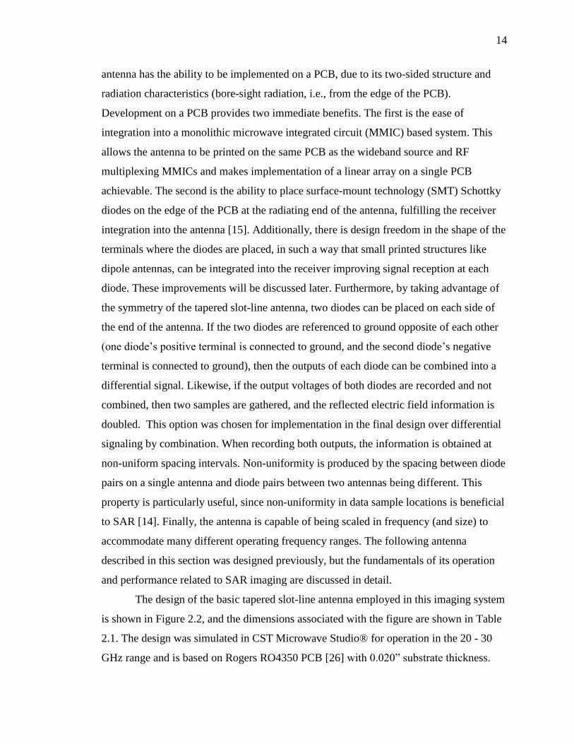
In addition to affecting the reflection coefficient characteristics across the band, it
is possible that the inclusion of the integrated receivers have an effect on the radiation
characteristics as well. Figure 2.9 shows the far-field radiation pattern at 25 GHz of the
designed antenna with the integrated mixer diodes.
By comparing the radiation characteristics of the antenna with and without the
receivers, it is clear that the receivers do not have a significant effect on direction of
radiation. Here, the radiation is still primarily in the bore-sight direction, as indicated in
red color around the y-axis. There exists low level variations in the radiation around the
+y-axis as indicated by the change in color from red to yellow which represents a
negative difference in gain. Radiation plots at different frequencies across the operating
band have mostly similar characteristics (Appendix A).
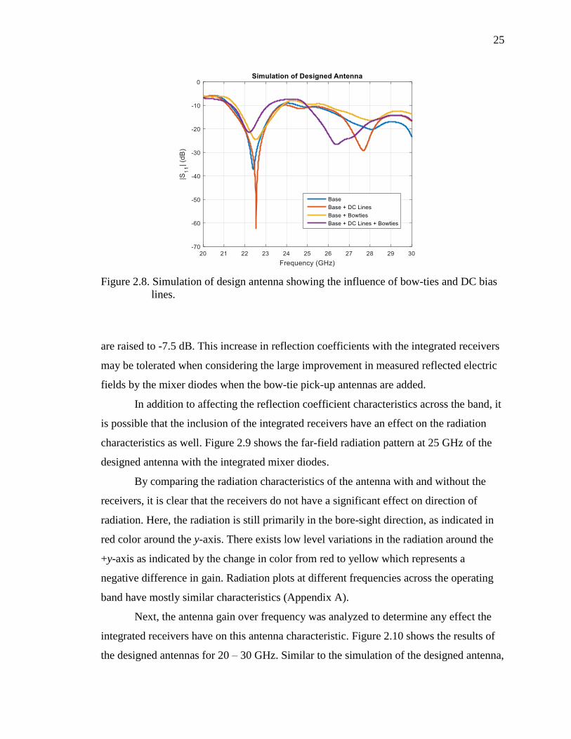
Next, the antenna gain over frequency was analyzed to determine any effect the
integrated receivers have on this antenna characteristic. Figure 2.10 shows the results of
the designed antennas for 20 – 30 GHz. Similar to the simulation of the designed antenna,
26
Figure 2.9. Far-field radiation of the designed antenna with receiver at 25 GHz.
Figure 2.10. Simulated bore-sight gain of the designed antenna with integrated receivers.
the gain of the antenna with the integrated receivers follows an increasing trend with
frequency. The reported gain is also in the same range of 0 to 11 dB with most of the
band between 4 and 11 dB with some slightly lower values, but this can be expected with

27
radiation losses and reflections due to the addition of the integrated receivers. Overall, the
receivers show to have minimal effect on the gain.
From these complete analyses of the antenna characteristics, it is clear that adding
receivers for the purpose of measuring reflected electric field far outweighs the slightly
diminished performance with the inclusion of integrated receivers.
With the analysis of the critical characteristics of the simulated antennas with
integrated receivers completed, it is important to investigate another antenna
characteristic in relation to SAR imaging. For the purpose of nondestructive testing,
synthetic aperture scanning is performed in the near-field and far-field regions of this
antenna [14]. However, for the case of operating in the near-field, the antenna and SUT
cannot be in contact or close to being in contact as this makes SAR focusing for these
distances irrelevant. Therefore, it is also important to understand the electric fields
radiating at short distances away from the antenna. For SAR, a wide beam of radiation is
desired to irradiate a large area on a SUT [14]. The tapered slot-line antenna has a wide
beam, but it is still relevant to determine if the integrated receivers have an effect on the
electric fields close to the antenna. In simulations, the complex electric field is mapped
from input into the antenna to 32 mm in front of the radiating end. The field is mapped at
25 GHz in two views: one from the top perspective of the antenna in Figure 2.11, and a
second looking into the radiating end of the antenna in the bore-sight direction in Figure
2.12.
In Figure 2.11, the electric field is seen traveling down the GCPW, through the
transitions, down the tapering slot-line, and out into air. Here, the bore-sight direction is a
horizontal vector moving to the right. The shape of each phase front in front of the
radiating end is spherical, and the intensity of the front decreases as the looking
perspective moves from bore-sight to the side of the antenna. This indicates gain in the
bore-sight direction.
For the perspective of looking into the radiating end of the antenna in Figure 2.12,
a change in color indicates a change in electric field amplitude. A circle with a solid color
indicates a region with nearly uniform amplitude. For a wide beam, the center of the
circle will be a solid color, and the change in color at the edge of the circle indicates the
edge of the radiation beam. Here, the change from green to blue is approximately 30 dB.

28
Figure 2.11. Electric field distribution at 25 GHz for the top view of the antenna.
Figure 2.12. Electric field distribution at 25 GHz for the bore-sight view of the antenna.
The electric field distribution is indicative of a wide beam of radiation with a
circular area of solid color centered in the middle of the image, and the color changes
gradually from green to blue. The fields mapped at other frequencies within the operating
band show similar spherical phase fronts (Appendix A). It is clearly shown the electric
fields radiated from the designed antenna with integrated receivers are sufficient for SAR
imaging.
2.1.2. Physical Layout. The three-element simulation was physically tested
exported to Cadence Allegro PCB Editor for fabrication. At the time of fabrication, the

29
bow-tie pick-up antennas were not optimized to their final dimensions, so the antenna
manufactured for testing contained slightly modified printed bow-tie antennas, where the
arms flared out at an angle slightly wider than 35°. As will be shown later, this small
variation in shape does not adversely impact the measured reflection coefficient
characteristics. The complete imaging system, however, used the design reported in
Figure 2.6.
Figure 2.13 (a) shows the PCB layout of the antenna. For testing, an array of three
antennas was manufactured with the center antenna fed by a connector to a wideband
source, and the side antenna inputs were matched terminated. The center antenna was
connected to an SMA PCB pad through GCPW transmission line. The DC bias lines for
both diodes on the center antenna were connected to 0.100” pitch through-hole connector
holes, so a cable could be soldered through and fed into a data acquisition system. The
manufactured antenna is shown in Figure 2.13 (b) and (c).
An SMA connector was soldered to the input terminal of the center antenna
followed by two wires soldered to the through-hole connector holes for sampling diode
voltages. Skyworks SMS7621-060 Schottky diodes were placed on each bow-tie pick-up
antenna of the center antenna arranged in the same configuration shown in the design
schematic to sample output voltages [28]. The bias lines were loaded with 200 Ω 0201
size choke resistors to attenuate high frequency signals coupled to the bias lines from the
ground plane underneath the lines on the opposite layer, as mentioned earlier. A 10 pF
Figure 2.13. (a) PCB layout generated in Allegro PCB Editor, (b) top view of fabricated
test antenna and (c) bottom view of fabricated test antenna.

30
capacitor and 10 kΩ resistor were added in parallel to each DC bias line at the connection
to coaxial cable and formed a basic low pass filter to attenuate high frequency signals on
the bias lines. The values for the low pass filter elements were given by the test circuit in
the Schottky diode datasheet.
2.1.3. Antenna Measurement. The manufactured antenna was first tested
for its reflection coefficient characteristics and gain in order to compare to the simulation
results shown earlier. The antenna was connected to a coaxial port of an Anritsu Vector
Star MS4644A vector network analyzer (VNA) through a coaxial cable. Prior to
conducting the measurements, the coaxial port was calibrated to the cable end where the
antenna was connected. The calibration procedure ensured reflection coefficient
measurements made in the measuring band (20 – 30 GHz) were referenced to the end of
the cable. After calibration was completed, the antenna was attached to the port, and the
VNA was set to transmit a wideband signal containing frequencies ranging from 20 to 30
GHz into the antenna and measure the reflection coefficient for each frequency in the
operating range. The antenna radiated into free-space with no objects in its vicinity that
could reflect signals back into it. Figure 2.14 shows the measured and simulated
reflection coefficient results.
Figure 2.14. Comparison of the measured reflection coefficients of the designed antenna
to simulation.

31
In comparison to simulation results, the measured reflection coefficient produced
a similar match but with improved matching in the 20 – 21.5 GHz range. The -7.5 dB
high reflection region moved higher in frequency. These changes are likely due to
increased electrical length of the antenna introduced by the SMA connector and section
of GCPW transmission line from connector to antenna. With increased electrical length,
the reflection coefficient at frequencies in the lower end of the band are improved, and
resonant features such as the -7.5 dB region shift in frequency.
For the gain measurements, Friis transmission formula was employed [27]. This
equation relates power transferred between two antennas to the gain of each antenna and
is denoted:
𝑃𝑟
𝑃𝑡= |𝑆21|2 = (
𝜆
4𝜋𝑅)
2
𝐺𝑡𝐺𝑟 (1)
Here, 𝜆 denotes operating wavelength, and 𝑅 corresponds to distance between
antennas. The value for 𝑅 was determined by measuring the distance between the
radiating ends of two antennas. Finally, 𝐺𝑡 and 𝐺𝑟 are the gains of each antenna. If the
transmitting and receiving antennas are like elements, the gain for like elements can be
found with 𝑆21 measurements at a certain frequency for a certain spacing between the two
antennas. It is important to note that these measurements must be made in the far-field
region of both antennas. The gain for this antenna was determined by aligning two
identical manufactured antennas, whose reflection coefficient characteristics were
measured to be the same, with the bore-sight direction of both antennas aimed at each
other. Each antenna was connected to a calibrated port of the Anritsu VNA, where both
cables were phase referenced similar to the reflection coefficient measurements. The 𝑆21
measurements, which determine the ratio of transmitted signal from one port to the
received signal of the second port, were used to determine power transfer between the
antennas. The experiment took place in a semi-anechoic chamber to ensure no reflections
from the surrounding area could interfere with the test. Multiple measurements were
taken with different distances ranging from 100 to 200 mm to get an average power
transfer value per frequency. Figure 2.15 shows this test setup.
The absorbing panels inside of the box attenuates signals passing through
isolating the antennas inside the box from the outside. Additionally, one of the antennas

32
Figure 2.15. Test setup for determining the power transfer between two like antennas.
was suspended from an arm made out of blue construction foam whose dielectric
properties are close to air. The arm moved one of the antennas towards and away from
the other antenna, allowing for multiple measurements at different distances. This setup
allowed for measurements with no metal around the antennas or interfering signals to
skew the measurements.
Figure 2.16 shows the resulting gain measurements and those obtained by the
simulations. While the measured gain follows a similar increasing trend with frequency,
there is some difference at some frequencies. Small variations in the gain can be
attributed to differences in the gain measurements for multiple distances, since they
produce fluctuations when the gain measurements are averaged together.
Additionally, the calculated gain can be lower than expected if either of the
antennas is not aligned in their respective directions of maximum radiation, or the
efficiencies of the antennas are lower than in simulation. Besides the slightly lower than
expected values, the gain for the manufactured antenna is acceptable since none of the
range has negative gain and there are no high fluctuations.
With gain and reflection coefficient characteristics known, the manufactured
antenna was tested, as a single raster-scanning probe, to determine its capability for
imaging. The far-field radiation pattern of the manufactured antenna was not measured,
since a chamber for facilitating far-field radiation pattern measurements for 20 - 30 GHz

33
Figure 2.16. Comparison of measured gain of the designed antenna to simulation.
was not available. Additionally, images generated by scans made with this antenna give
an indication of its radiation characteristics. The antenna was connected to a 10 dBm 22 -
27 GHz signal generator and mounted to an arm of a mechanical scanning table. The
reason for limiting the operating frequency range of the test scanning was to match the
frequency range that was available from MMIC based RF sources that would be used
later in the system. The output of each diode was connected to data acquisition hardware.
The antenna raster scanned a small metal ball located 12 mm under the antenna on a 50
mm x 50 mm area with 2 mm spacing increments. After the raster scan was performed,
the collected diode voltages were processed using the SAR algorithm, and an image was
produced and focused at the location of the metal ball. Figure 2.17 shows the
antenna scanning over a small area. Figure 2.18 (a) and (b) show the 2D slices of the
metal ball with data collected from the left and right (upper and lower from Figure 2.6)
diode respectively.
For both images, the metal ball can be clearly seen against the background. Also,
the indication of the metal ball follows a similar round shape. The images generated by
the test antenna confirm the ability to irradiate a SUT and map the reflected electric field
with reasonable accuracy.

34
Figure 2.17. Designed antenna raster scanning over a small area.
Figure 2.18. (a) Image generated with left diode. (b) image generated with right diode.
2.2. ARRAY DESIGN
2.2.1. Signal Flow Design. With the completion of the antenna element
design, the linear array was designed. The hardware connecting the array antenna
elements can be broken down into two circuits: transmitter multiplexer and receiver
multiplexer. The transmitter multiplexer switches all antennas to a single wideband
source. The receiver multiplexer encodes all diodes voltages from all antennas into a
central output channel. A sixteen-element array was chosen for this work since two levels
of SP4T MMIC switches can be used to multiplex the wideband source to one of sixteen
antennas. Multiplexing DC voltages from the integrated receivers of one of the sixteen
antennas can be accomplished with a single chip [25]. Figure 2.19 shows the RF signal
flow diagram for the sixteen element array.
X (mm)
Y (
mm
)
Board 1, Channel A
0 20 400
20
40
5
10
15
20
X (mm)
Y (
mm
)
Board 1, Channel B
0 20 40
10
20
30
40
50
20
40
60
80
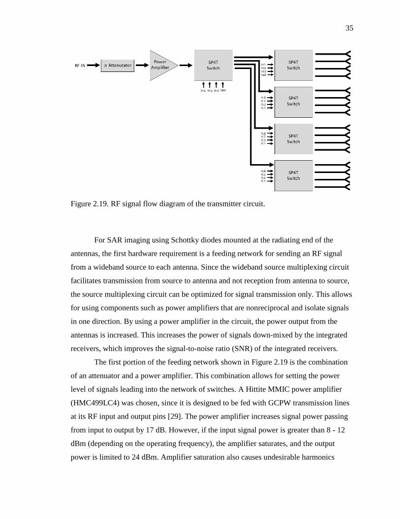
35
Figure 2.19. RF signal flow diagram of the transmitter circuit.
For SAR imaging using Schottky diodes mounted at the radiating end of the
antennas, the first hardware requirement is a feeding network for sending an RF signal
from a wideband source to each antenna. Since the wideband source multiplexing circuit
facilitates transmission from source to antenna and not reception from antenna to source,
the source multiplexing circuit can be optimized for signal transmission only. This allows
for using components such as power amplifiers that are nonreciprocal and isolate signals
in one direction. By using a power amplifier in the circuit, the power output from the
antennas is increased. This increases the power of signals down-mixed by the integrated
receivers, which improves the signal-to-noise ratio (SNR) of the integrated receivers.
The first portion of the feeding network shown in Figure 2.19 is the combination
of an attenuator and a power amplifier. This combination allows for setting the power
level of signals leading into the network of switches. A Hittite MMIC power amplifier
(HMC499LC4) was chosen, since it is designed to be fed with GCPW transmission lines
at its RF input and output pins [29]. The power amplifier increases signal power passing
from input to output by 17 dB. However, if the input signal power is greater than 8 - 12
dBm (depending on the operating frequency), the amplifier saturates, and the output
power is limited to 24 dBm. Amplifier saturation also causes undesirable harmonics

36
called third order intercept (IP3) that should be avoided. Therefore, the attenuator placed
before the amplifier allows for reducing the signal level input into the amplifier to avoid
saturation. The 𝜋 – attenuator was chosen since it can be printed on a circuit board with
only three small surface mount resistors.
One disadvantage of this MMIC amplifier is the requirement for power
sequencing between the negative and positive voltage supplies. The negative voltage
supply required -0.8 V to open a transistor gate inside the chip. If the positive 5.0 V
supply were to connect before the negative supply opened the gate, the chip would sink
high positive supply current and burn the chip. This required a power sequencing circuit
shown in Appendix B.
After the RF signal is amplified, it is routed to one of the antennas through two
levels of SP4T switches. For this purpose, a Hittite MMIC switch (HMC1084LC4) was
chosen for its small profile similar to the power amplifier [30]. The use of this switch is
attractive since it provides a 30 dB isolation between switch outputs and due to its simple
switching control scheme. To switch to one of the outputs, a gate for the specified output
was driven with a negative voltage while the other switch inputs were grounded. These
gate pins for driving a switch are shown as VH1 – VH4 and VL1 – VL4 for the high level
and low level switches, respectively. The negative driving voltage required a voltage
inverting circuit shown in Appendix B. The benefit of this approach is the ability to drive
8 logic lines with CMOS technology (3.3 V), invert the 3.3 V signal to -3.3 V, and switch
to one of the sixteen antennas in the array. This allowed for electronic switching by many
popular microprocessors using CMOS technology for their general purpose input/output
control lines.
The second hardware requirement for SAR imaging using Schottky diodes, is a
multiplexing network for sampling diode voltages. The first design challenge for
accomplishing this goal is routing the network of output voltages (two output channels
per antenna/sixteen antennas per array) to a multiplexing circuit. This was accomplished
by bonding the PCB containing the feed network and array of antennas to a second
“daughter” PCB containing a low frequency multiplexer circuit. Figure 2.20 shows this
combination of PCBs. The output voltages from each antenna are first routed away from
the antenna aperture and are terminated in vias. Corresponding vias on the daughter board

37
are aligned with the array board forming a direct electrical connection when the aligned
vias are soldered through. The voltage lines at the vias on the daughter board are then
routed into a multiplexing circuit. This method of transferring signals from board to
board is also used for the eight logic lines associated with the RF switches and for the
power amplifier voltage supply.
The multiplexing circuit used to encode all 32 output voltages from the array
board is shown in Figure 2.21. The positive and negative voltage outputs from each
antenna are grouped with their respective polarities and fed into a central multiplexer.
When a particular antenna is selected, its positive and negative voltage pair is passed
through the multiplexer and out to an SMA connector to feed the data acquisition
Figure 2.20. The antenna array PCB and a supporting board are bonded together through
vias.
Figure 2.21. Diagram for encoding multiple diode voltages to two common channels.

38
hardware. This was accomplished using the Analog Devices ADG726 Analog
Multiplexer IC [31]. This chip allows for selecting an antenna’s diode voltages to pass
through by simply providing the 4-bit binary representation of 0 – 15, which correspond
to the location of an antenna along the array, shown in the figure as A0 – A3. An
additional attractive feature of this multiplexer is its ability to operate using a
positive/negative rail at ± 2.5 V, which allows for both positive and negative output
voltages to pass through. The logic lines of the multiplexer and RF signal switches were
terminated in a rectangular header connector for direct connection to a PC or
microprocessor. The complete schematics for both the antenna array board and daughter
board are shown in Appendix B.
2.2.2. Array Simulations. While the performance of the designed antenna
was assessed for operation as a three element array, one radiating antenna and two
matched elements, this section evaluates the designed antenna in the presence of the full
sixteen element array. With a sixteen element array, the radiating beam of the active
antenna can be wider, narrower, or slightly shifted from bore-sight direction. After the
array was manufactured, a metallic shield was attached to the linear array to prevent the
RO4350 PCB from bending, since this board is only 0.020” thick. Radiation
characteristics can change significantly in the presence of a metallic shield. The
surrounding conditions of an operating antenna must be assessed to predict how it would
radiate after the imaging array is fabricated.
The array was based on simulation of the base antenna which was duplicated to
form an eighteen element array (sixteen functional antennas, and two non-functional end
antennas). Two matched antennas were placed on each end of the array, so an antenna on
the end of the sixteen element array would have one element on each side to match the
three-element array simulation. Two cases were simulated: the array with no metallic
shield, and the array with metallic shield. On each end of the array, a small portion of
PCB (13 mm wide) was added, so the metal shield could be attached to each end of the
array. For simulation with a shield, a metallic structure was added above the array,
behind the aperture. Figure 2.22 shows the simulation model with and without the metal
shield. For both cases, a wave port was placed at a center antenna, which simulates a
center antenna radiating.

39
(a)
(b)
Figure 2.22. Simulation model of the full array: (a) without a shield and (b) with a shield.
Figure 2.23 shows the radiated electric fields with and without the metal shield. It
is clear for both cases that the presence of the full array still maintains good electric field
propagation from a center antenna. Much like the simulation of the designed antenna, the
electric fields propagate with a wide beam. However, the addition of the metal shield
slightly narrows the radiated beam. This can be attributed to the metal above and around
the array directing the radiation into a narrower beam. The metallic boundaries alter the
surface currents on the sides of the array. This change results in a reduction of radiation
from the sides of the array and results in a narrower main beam. Appendix B shows
simulations at multiple frequencies for both simulation cases. Regardless of the presence
of a shield in the surrounding area, the antennas operating in the full array have good
radiation characteristics for electric field mapping.

40
(a)
(b)
Figure 2.23. Simulated electric fields at 25 GHz of the full array (a) without a shield and
(b) with a shield.
2.2.3. Array Fabrication. The antenna array was fabricated in the same way
as the tested design antenna. The array was drafted in Allegro PCB Editor and printed on
two-layer Rogers RO4350 0.020” PCB substrate. The daughter board was drafted
similarly but fabricated on FR-4 0.060” substrate. Since the daughter board only
contained digital lines, power regulation, and analog DC voltages, there was no need to
use a high performance substrate, so the FR-4 was used. Figure 2.24 displays the
fabricated and assembled boards and metallic shields.
Both boards were fabricated and assembled by Hughes Circuits, Inc. Upon arrival,
the antenna array board and daughter board were bonded at each via by filling the inner
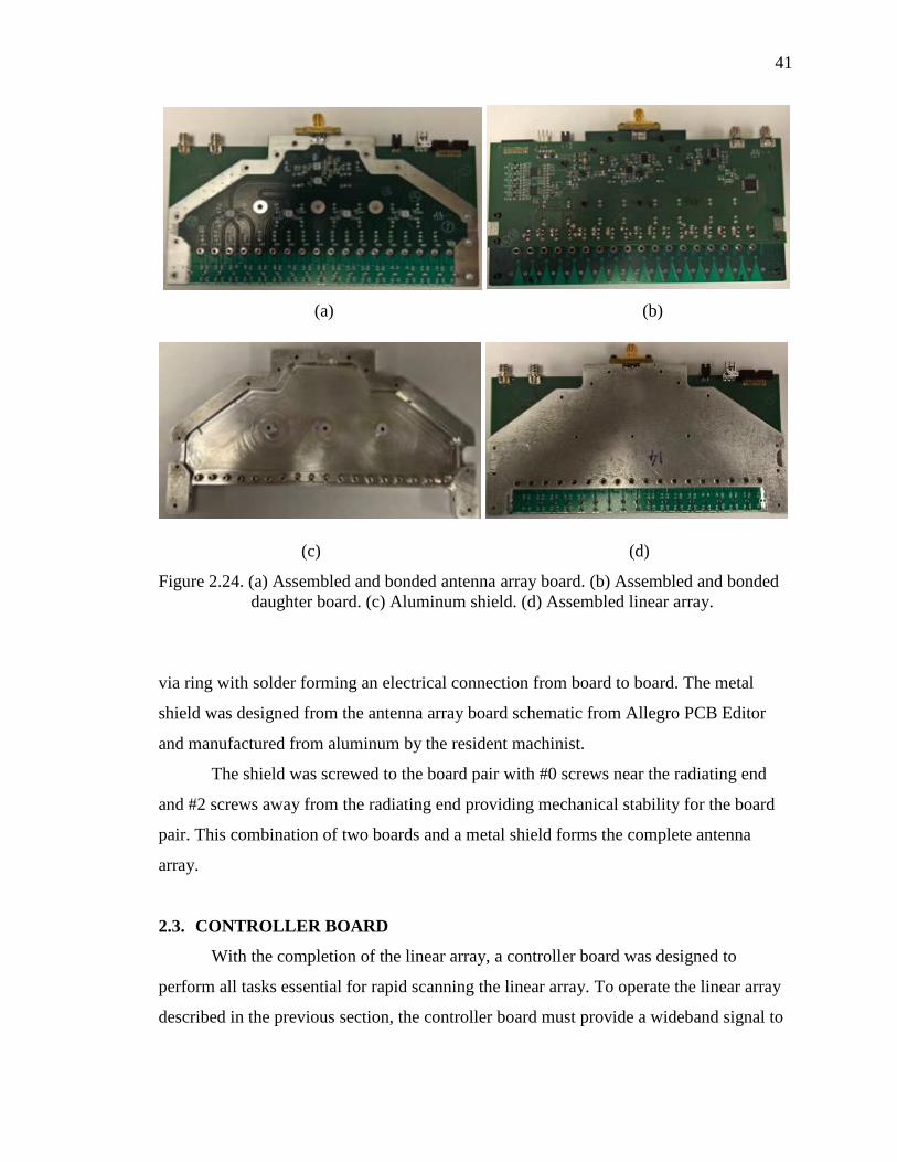
41
(a) (b)
(c) (d)
Figure 2.24. (a) Assembled and bonded antenna array board. (b) Assembled and bonded
daughter board. (c) Aluminum shield. (d) Assembled linear array.
via ring with solder forming an electrical connection from board to board. The metal
shield was designed from the antenna array board schematic from Allegro PCB Editor
and manufactured from aluminum by the resident machinist.
The shield was screwed to the board pair with #0 screws near the radiating end
and #2 screws away from the radiating end providing mechanical stability for the board
pair. This combination of two boards and a metal shield forms the complete antenna
array.
2.3. CONTROLLER BOARD
With the completion of the linear array, a controller board was designed to
perform all tasks essential for rapid scanning the linear array. To operate the linear array
described in the previous section, the controller board must provide a wideband signal to

42
feed into the array, perform the logical operations to multiplex the RF switches and
output diode voltage multiplexer, and provide an information path for recording scan data
to a PC. This was accomplished by designing several key modules on one board:
interface to microcontroller, diode voltage sampling circuit, digital to analog converter
for RF source frequency tuning, and RF transmitter. Figure 2.25 shows a basic layout of
such board.
The imaging system required connection to a PC to gather the scan data upon
completion of a scan. Additionally, programmable hardware was required for controlling
the array multiplexing through software. To this end, the controller board was connected
to a microprocessor to perform these tasks. An interface to a microprocessor was first
designed and consisted of a pair of rectangular pin connectors to connect to the input /
output lines of a microprocessor. The unit chosen for operating this system was the
Beaglebone Black microprocessor [32]. This system is designed around the Texas
Instruments AM355X 1 GHz ARM Cortex A8 chip processor [33]. The advantage of
using this platform was the ability to write the software that controls the linear array on
the Linux operating system Debian directly into the microprocessor. Additionally, the
Beaglebone contains over 60 general purpose input / output ports for digital logic
Figure 2.25. Block diagram displays the various modules of the controller board.

43
operations and two programmable real-time unit (PRU) microcontrollers for high speed
connection to the diode voltage sampling circuit. Two 46-pin rectangular header
connectors connected the Beaglebone to the control board.
The second module of the control board is the mixer diode voltage sampling
circuit shown in Figure 2.26. The positive and negative analog voltages produced by the
integrated receivers are converted to digital signals through two analog-to-digital
converters (ADCs). Each ADC was responsible for converting one of the analog channels
and outputting a digital signal to the Beaglebone for recording to a file on a PC. The
ADC chosen was the Analog Devices AD7621 ADC, which operated on the successive
approximation technique for conversion [34]. The functionality of this IC is attractive for
its 16-bit output and 2 MSPS (mega sample per second) conversion speed. This allowed
for recording input signals quickly and accurately. Since the ADC input was differential,
a set of operational amplifiers was used before the signal, which was referenced to
ground, was read into the ADC. For the positive channel, a single to differential non-
inverting gain op-amp amplified 0 – 0.25 V signals to 0 – 2 V differential signals
common to 1 V. If a receiver produced a 0.125 V DC signal, which covers half of the
input range of the op-amp input, the op-amp would produce 1.5 V and 0.5 V DC voltages
that feeds into the positive and negative inputs of the ADC, respectively, covering half of
the input range of the ADC. Similarly, for the negative channel, the same system was
used but with polarity inversion to change the negative input voltages to positive outputs.
Figure 2.26. Block diagrams of the diode voltage sampling circuit.
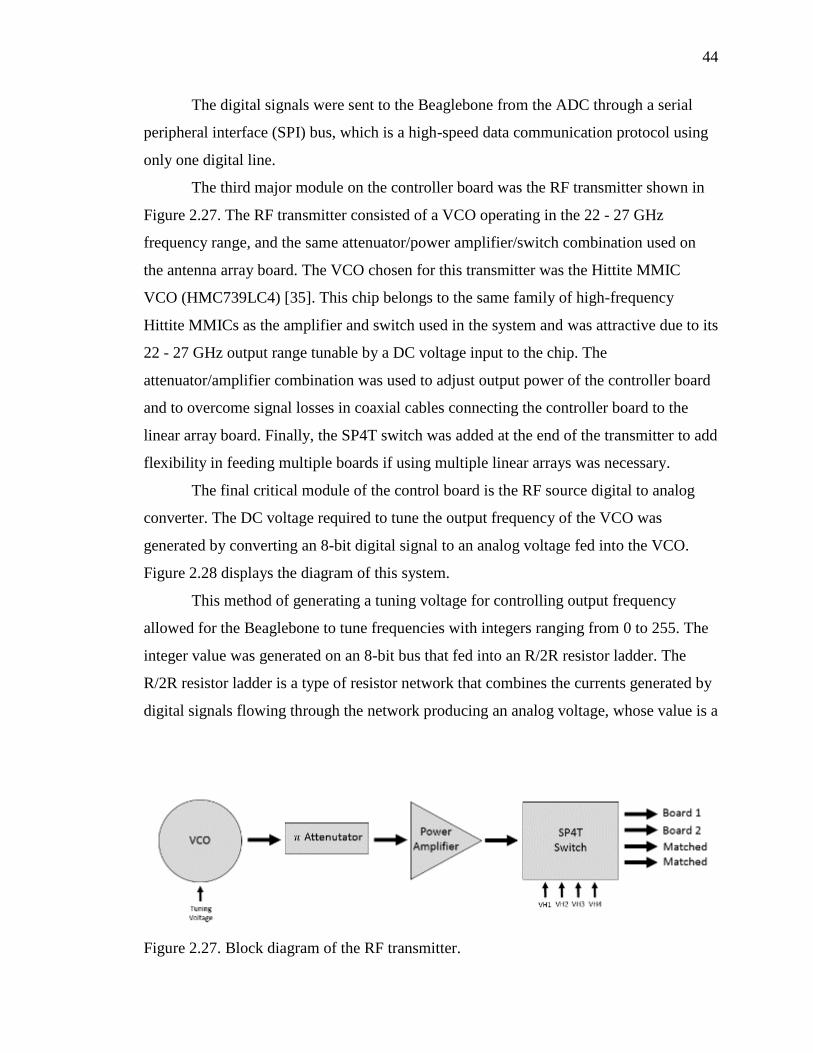
44
The digital signals were sent to the Beaglebone from the ADC through a serial
peripheral interface (SPI) bus, which is a high-speed data communication protocol using
only one digital line.
The third major module on the controller board was the RF transmitter shown in
Figure 2.27. The RF transmitter consisted of a VCO operating in the 22 - 27 GHz
frequency range, and the same attenuator/power amplifier/switch combination used on
the antenna array board. The VCO chosen for this transmitter was the Hittite MMIC
VCO (HMC739LC4) [35]. This chip belongs to the same family of high-frequency
Hittite MMICs as the amplifier and switch used in the system and was attractive due to its
22 - 27 GHz output range tunable by a DC voltage input to the chip. The
attenuator/amplifier combination was used to adjust output power of the controller board
and to overcome signal losses in coaxial cables connecting the controller board to the
linear array board. Finally, the SP4T switch was added at the end of the transmitter to add
flexibility in feeding multiple boards if using multiple linear arrays was necessary.
The final critical module of the control board is the RF source digital to analog
converter. The DC voltage required to tune the output frequency of the VCO was
generated by converting an 8-bit digital signal to an analog voltage fed into the VCO.
Figure 2.28 displays the diagram of this system.
This method of generating a tuning voltage for controlling output frequency
allowed for the Beaglebone to tune frequencies with integers ranging from 0 to 255. The
integer value was generated on an 8-bit bus that fed into an R/2R resistor ladder. The
R/2R resistor ladder is a type of resistor network that combines the currents generated by
digital signals flowing through the network producing an analog voltage, whose value is a
Figure 2.27. Block diagram of the RF transmitter.

45
Figure 2.28. Block diagrams of the RF source digital to analog converter.
function of the digital signals. When connected to the digital lines from a Beaglebone, the
digital signal is 3.3 V for the high state and 0 V for the low state. By feeding the most
significant bit into the highest position in the ladder and progressively filling the lower
ladder rungs with lesser significant bits, the output pin of the R/2R ladder generates
analog voltages in the 0 – 3.3V range directly proportional to the input integer. To utilize
the full tuning range of the VCO (0 – 10 V), a non-inverting gain op amp amplified the
R/2R output creating a digital to analog conversion system capable of converting a 0 –
255 integer into a 0 – 10 V DC signal.
The control board contained many other smaller circuits necessary for operating
these high level modules and are reported in Appendix C along with the complete circuit
diagrams of the control board. Like the other PCBs designed for this system, the
controller board was designed in Allegro PCB Editor on FR-4 0.060” substrate. Figure
2.29 displays the assembled board. This board is seated directly on the Beaglebone Black
and performs all essential operations for supporting the antenna array.
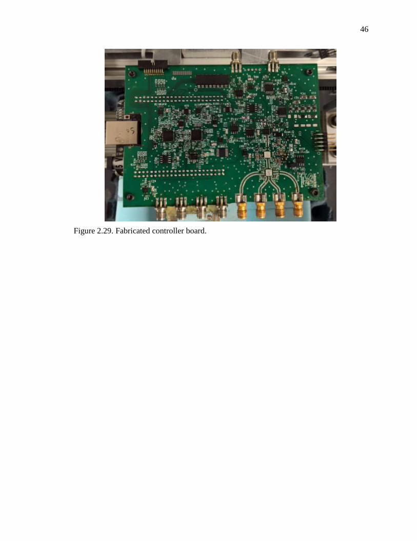
46
Figure 2.29. Fabricated controller board.

47
3. SYSTEM TEST
The imaging system designed and fabricated for this investigation was tested to
verify its rapid image data collection capability. Section 3.1 describes the steps taken to
establish a hardware and software testing environment for imaging with this system. The
system was first attached to a mechanical scanning system outlined in Section 3.1.1.
Next, software was written to control the mechanical and electronic scanning and is
discussed in Section 3.1.2. The system was then calibrated with receiver equalization
shown in Section 3.1.3. In Section 3.1.4, the addition of a second linear array for
eliminating aliasing in images is discussed. Finally, targets scanned by the calibrated and
optimized system are shown in Section 3.2.
3.1. MEASUREMENT SETUP
3.1.1. Scan Table. The first step towards testing the imaging system is
attaching it to a mechanical scanning table. Since the purpose of this imaging system is to
electronically scan in one direction and mechanically scan in the perpendicular direction,
the imaging array and its controller board must be attached to a scanning table capable of
moving the combination of boards along one dimension. Figure 3.1 shows the scanning
process over a sample under test (SUT).
To facilitate the one dimensional movement of the linear array and controller
board, the system was attached to a small scan table capable of mechanically scanning in
one or two orthogonal dimensions, as shown in Figure 3.2.
With this table, the imaging system is mounted on a bracket (not shown) that
moves in two orthogonal directions with two stepper motors. The array board is mounted
to the side of the movable bracket with radiating end of the board (direction of antenna
array radiation) pointed down to scan a SUT that is placed below the table. The controller
board rests on top of the bracket, enabling the entire imaging system to move with the
bracket. The first stepper motor controls the movement in the X-direction (as indicated
with the red arrow in Figure 3.2) by moving two pulleys on the side of the table. These
pulleys move a horizontal bar that sits on two tracks. The bar holds the second stepper
motor and the imaging system sitting on a bracket. The second stepper motor controls

48
Figure 3.1. Linear imaging array scanning along a SUT.
Figure 3.2. Imaging system attached to small scanning table (view from top).

49
the Y-direction movement (also indicated in Figure 3.2) by moving the bracket along the
horizontal bar. In this case the second motor is not used, since scanning along the Y-
direction is performed electronically by the array. The motors are connected to solid state
drivers, which are controlled by a PC, automating the mechanical scanning process. After
mounting the imaging system to the scan table, there is approximately 100 mm of
distance along the X-direction that can be used for the mechanical scan. With the 120 mm
dimension of the imaging array, the total scanning area of the system is 120 mm by 100
mm.
3.1.2. Scanner Software. With the imaging system mounted to a scan table, a
software package was written to control the electronic and mechanical scanning. The
software is composed of three components: LabVIEW™ virtual panel, assembly code,
and C-code. The LabVIEW™ interface is installed on a PC and controls the X-stepper
motor. It also sends command signals to the controller board for initializing the electronic
scanning process. This interface provides the operator with a view of the raw data from
the imaging system as it is streamed from the Beaglebone microprocessor. The assembly
code is installed on the Beaglebone and instructs the programmable real-time unit
microcontrollers (PRUs) to electronically scan along the array. The C-code is also
installed on the Beaglebone and works as an intermediary between LabVIEW™ and
assembly code. The procedure for performing a scan is shown below in several steps.
Step 1: LabVIEW™ commands the X-stepper motor to position the linear array to
a scanning location and commands the Beaglebone to begin the electronic scanning
process.
Step 2: Assembly code instructs PRUs to multiplex the first antenna in the array
to the wideband source on the controller board and receivers on the first antenna to the
analog to digital converters, also on the controller board.
Step 3: C-code steps through a list of frequencies, where the source is tuned to
sequentially output each frequency in the list. These frequencies are set by the
LabVIEW™ interface. The frequency range was set for 21.5 to 27 GHz with 201
frequency points. After the antenna has continuously radiated at the tuned frequency for a
short time period (~2-3 nano seconds), the ADC converts the output voltages of the

50
receivers on the antenna to digital voltages and sends the data to the Beaglebone to be
recorded.
Step 4: Steps 2-3 are repeated for each antenna in the array.
Step 5: After cycling through all antennas in the array, the C-code sends the
recorded voltages from all antennas for all frequencies to LabVIEW™ and signals a
completion of the electronic scan.
Step 6: Steps 1-5 are repeated for all mechanically scanned locations.
Step 7: After all mechanically scanned locations are finished, all recorded data is
saved to a file on a PC.
3.1.3. Array Equalization. An issue that occurs when scanning with an
array of antennas vs. scanning with a single antenna is the difference in signal levels
among antennas. When a single antenna is raster scanned over a 2D grid, the antenna
radiated signal (power) level at the antenna input port is constant for each location.
However, when an array of antennas is used, the power levels of signals at all antenna
input ports are different. This is due to different transmission line lengths to all antenna
input ports, slight differences in antenna configurations, etc. Also, different insertion
losses between the inputs and the outputs of the SP4T switches used in the wideband-
source-to-antenna multiplexing circuit cause differences in the power levels of signals.
This problem is further complicated when using Schottky diodes as the basis of the
integrated receivers. The frequency response of a Schottky diode is never the same from
one diode to the next, so the outputs from receivers across all antennas will differ.
With many factors contributing to differences in values in the recorded data from
the receivers on the linear array, an equalization matrix was generated and applied to the
raw data of a scan. The equalization matrix is a 2D matrix with the first dimension
representing the antennas in the array and the second dimension representing all
frequencies generated by the wideband source. By equalizing the raw data from a scan,
the signal levels across all antennas and across all frequencies are normalized to 1. Each
value in the raw data corresponds to a specific receiver for a particular frequency. By
dividing each data point in the raw data by the equalization value corresponding to the
same receiver and frequency, the resulting data is equalized.

51
Generating the equalization matrix was completed with a moving metal plate
calibration. A metal plate is considered a known target, and when the linear array scans
over a metal plate, all signals are reflected back towards the array. During this scan, the
voltages generated by the integrated receivers on all antennas are recorded and represent
the characteristic non-equalized output of the imaging array. Figure 3.3 shows a visual
representation of the experiment for one antenna.
While this figure does not show the electric fields adding to 0 on the metal, this is
the actual case, which results in total reflection of fields incident upon the metal plate.
For this experiment to work correctly, the direction of propagation of the radiated electric
fields must be orthogonal to the plane of the metal plate surface. If the metal plate was
tilted in any way, the direction of propagation of the reflected electric fields would be
away from the array. Even with the wide beam of the tapered slot-line antenna, this
results in a lower signal power of the reflected fields picked up by the array.
In addition to sensitivity to incidence angle between array and metal plate, the
distance between the array and plate and frequency of operation influences the reflected
electric field. The radiated and reflected electric fields form a standing wave between the
Figure 3.3. Visual representation of an antenna radiating in the direction of a metal plate.

52
array and metal plate. The amplitude of the standing wave is a function of distance
between plate and array and frequency of operation. By moving the array and measuring
the voltages at the integrated receivers, the resulting voltages picked up by the receivers
oscillate with a sinusoidal shape as a function of distance. Furthermore, as this distance
increases, the received voltages amplitudes decay proportional to the inverse fourth
distance between array and metal plate. For the scope of this investigation, the
equalization matrix was formed with the output voltages averaged over distance between
linear array and metal plate. However, future investigations can be made for using the
envelope of the output voltages as a function of distance to possibly improve the
equalization of the linear array.
The moving plate experiment was conducted with the linear array and is shown in
Figure 3.4. For this experiment, the linear array was scanned over the metal plate for
distances of 5 to 50 mm between the array and metal plate. Receiver voltages were
recorded for all antennas at all operating frequencies. Figure 3.5 shows one output
voltage curve for an arbitrarily chosen antenna and operating frequency (at 24 GHz).
In Figure 3.5, the sinusoidal variation and voltage decay as a function of distance
can be seen. However, the voltages deviate from the exponentially decaying envelope in
several locations. The most likely cause for this deviation is that there could exist
Figure 3.4. A metal plate is scanned by the linear array.

53
Figure 3.5. Output voltage of the one of the receivers on the eighth antenna in the array at
approximately 24 GHz.
multiple reflections between the antennas, metal plate, and surrounding test setup.
Additional reflections would raise or lower the recorded voltage, which would cause this
issue. These results are averaged over many scans, and these differences between the
expended envelope and measured envelope are the primary reason why the envelope was
not considered when forming the equalization matrix. The resulting output voltages for
all antennas at all operating frequencies were averaged with respect to distance between
plate and array and were tabulated into the equalization matrix.
3.1.4. Addition of a Second Linear Array. After the equalization matrix
was formed, the completed imaging system scanned over different targets. However,
aliasing became an issue with the images generated from the recorded data. In a 2D
image, artifacts of aliasing manifest as duplicates of the SUT positioned above and below
the real SUT along the scanning dimension that experiences aliasing. In this case, aliasing
occurred in the electronic scan dimension along the linear array since the distance
between two receivers on one antenna is 5.6 mm. At 27 GHz, which is the high end of the
operating frequency range, 5.6 mm is slightly larger than one-half of the operating
wavelength, which is approximately 5.5 mm. This resulted in some slight aliasing effects.
Artifacts of aliasing are easy to see when scanning a metal ball. The imaging system

54
scanned over a small metal ball located 30 mm away from the radiating end of the array.
Figure 3.6 shows the image of the metal ball with additional artifacts of aliasing. In this
figure, artifacts of aliasing are seen as faint duplicates of the small metal ball above and
below the actual metal ball.
Artifacts of aliasing were removed by attaching a second linear array behind the
first array and measuring reflected fields at locations between the receivers of the first
array. By interlacing two linear arrays, the distance between receivers is effectively
reduced to half. During the design process for the controller board, the ability to operate
up to two linear arrays simultaneously was added as well. The addition of the SP4T
MMIC switch in the RF transmitter circuit and the 2:1 analog multiplexer shown in
Appendix C provided the flexibility of operating one of two arrays. The second array was
mounted to the same bracket holding the first array and was positioned 12 mm behind the
first array and shifted to the right by 4 mm. Figure 3.7 shows how adding a second array
shifted to the right along the electronic scan dimension by 4 mm creates an overall
electronic scan with sample points spaced at 1.6 mm and 2.4 mm increments.
In Figure 3.7, the Xs represent the location of the receivers along each array.
When the second array is added and shifted to the right by 4 mm, the sample points of the
Figure 3.6. Image of a small metal ball with image data from the linear array.

55
electronic scan are 1.6 mm and 2.4 mm, which is much smaller than one-half of the
operating wavelength for all frequencies in the operating band. The moving metal plate
calibration was performed for two arrays, and the equalization matrix was recalculated to
accommodate two arrays. The same metal ball was scanned with the two arrays, and
Figure 3.8 shows the improved image.
Figure 3.7. Receiver sample points with two linear arrays.
Figure 3.8. Image of a small metal ball with image data from two linear arrays.

56
From this figure, it is clearly shown that the addition of a second array removes
the artifacts of aliasing. Additionally, the smaller distance between sample points resulted
in a higher resolution image. All test images generated by the imaging system after this
point were from the combination of two linear arrays.
3.2. IMAGING RESULTS
Several objects were imaged to show the rapid imaging capability of this system.
All measurements were made with the improved two linear array system. Also, the
measurements were made with 1 mm spacing increments in the mechanical scan
dimension. The operating frequency band was set to 21.5 – 27 GHz for the wideband
source. The low end of the frequency sweep was moved from 22 GHz to 21.5 GHz, since
the RF transmitter circuit was capable of producing frequencies down to 21.5 GHz.
Additionally, the designed antenna performed adequately at 21.5 GHz in terms of
reflection coefficient and gain. The equalization matrix was applied to the raw data, and a
scan of air was subtracted out prior to subjecting the raw data to the SAR algorithm. With
these scan parameters, the total scanning time for each image production was 48 seconds.
All SUTs were scanned with foam underneath, which has a dielectric constant close to 1,
so there were no strong reflections from below the SUT.
For 3D representation, the images are presented in a color scale of various shades
of orange, where black indicates no reflections from a target, and a bright orange color
indicates high reflection from a SUT. Similarly, for 2D representation, the images are
presented in gray-scale with similar intensity scaling.
3.2.1. Foam with Rubber Inclusions. The first imaged sample is made of low
dielectric construction foam with nine rubber inclusions distributed at different depths
inside the foam (Figure 3.9). This figure shows that on the top side of the foam block,
three rubber inclusions are visible. However, on the bottom side, there are no visible
inclusions. The six remaining inclusions are located inside the block. The rubber
inclusions are 5 mm in diameter and approximately 2 mm thick, and they are distributed
in groups of three. Each group is positioned at a different depth within the foam. The first
group seen in Figure 3.9 are at the surface level. The second and third groups are located
15 mm and 45 mm deep inside the block, respectively. Figure 3.10 shows the 3D

57
isometric view of the rubber inside the sample with a scan made over the top side of the
block. Rubber has a dielectric constant ranging from 5 to 9 depending on the particular
type, but all rubber types within this range have a relatively higher dielectric contrast
compared with the foam. The first two rows of rubber pieces are shown clearly, since
they are closer to the linear array. The third row is harder to see, since it is much farther
away from the linear arrays in comparison to the other two rows of rubber.
(a) (b)
Figure 3.9. (a) Top view and (b) bottom view of construction foam with nine rubber
inclusions.
Figure 3.10. 3D isometric view of the 9 rubber inclusions inside construction foam.
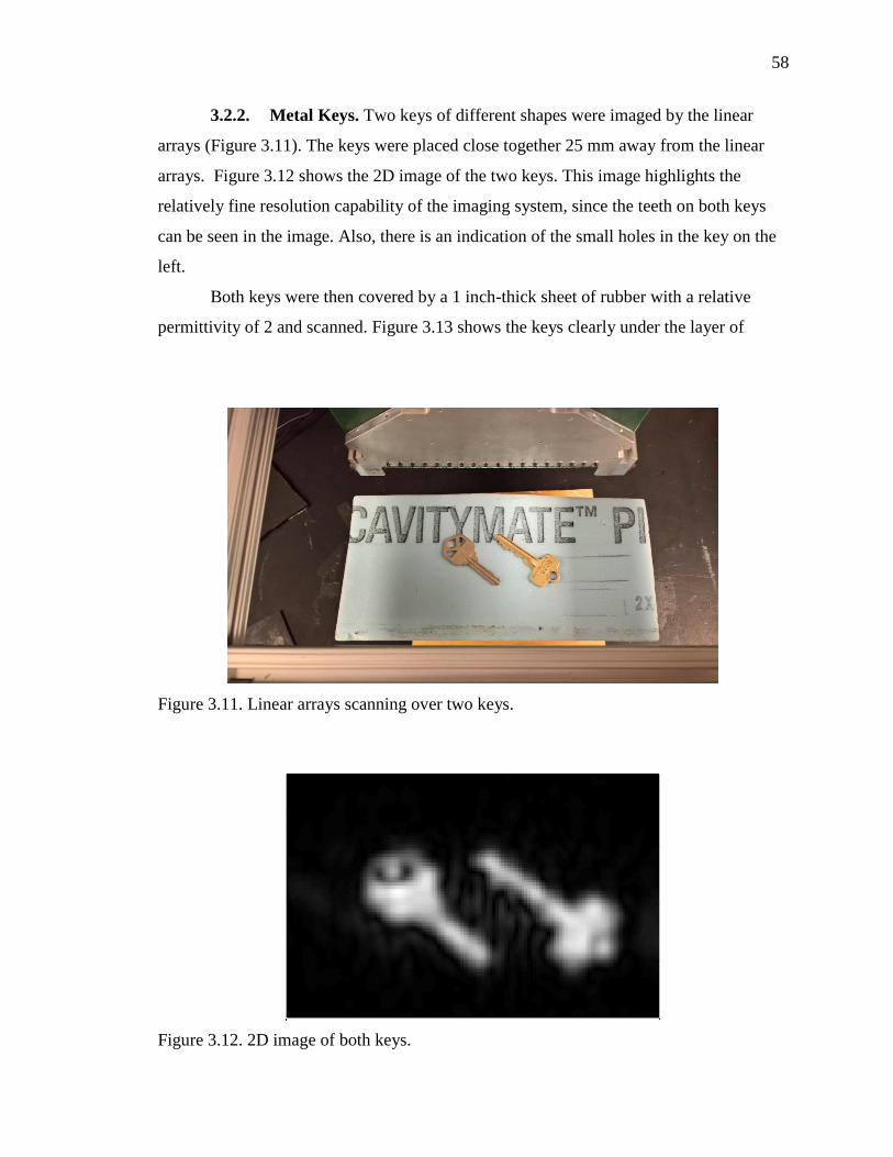
58
3.2.2. Metal Keys. Two keys of different shapes were imaged by the linear
arrays (Figure 3.11). The keys were placed close together 25 mm away from the linear
arrays. Figure 3.12 shows the 2D image of the two keys. This image highlights the
relatively fine resolution capability of the imaging system, since the teeth on both keys
can be seen in the image. Also, there is an indication of the small holes in the key on the
left.
Both keys were then covered by a 1 inch-thick sheet of rubber with a relative
permittivity of 2 and scanned. Figure 3.13 shows the keys clearly under the layer of
Figure 3.11. Linear arrays scanning over two keys.
Figure 3.12. 2D image of both keys.
X (m
m)
Y (mm)
Tw
o k
eys
020
40
60
80
0
20
40
60
80
100
120
0.0
5
0.1
0.1
5
0.2
0.2
5
0.3

59
Figure 3.13. 2D image of both keys covered with a 4 mm sheet of rubber.
rubber. Moreover, there is little difference in the resulting images with and without
rubber covering the keys. These images highlights the system’s ability to image metal
targets under dielectric materials.
3.2.3. Rubber Sheet with Voids. One important object imaged for
nondestructive evaluation applications is rubber with voids, where voids are air pockets
injected into rubber. Figure 3.14 shows a sheet of rubber with slots and holes cut out. The
cuts are approximately 50 mm long and 3 mm wide. The smallest holes are 5 mm wide,
and the mid-sized holes are 12 mm wide. The mid-sized holes are not drilled completely
through to test for detected depth in a rubber void. Finally, the sample contains a large
hole 30 mm wide drilled halfway through the sheet with a 6 mm hole drilled all the way
through. The first scan is made with the rubber sheet 25 mm from the linear arrays
(Figure 3.15). Here, all voids can be seen, but the partially drilled mid-sized holes cannot
be differentiated from the holes cut all the way through the sample. This is due to the
edges of these holes overshadowing the rubber that is inside. This edge effect is also
shown as the ring around the edge of the largest hole. Next, the rubber was imaged with a
1 inch-thick sheet of rubber with a relative permittivity of 2 placed on top of the sample
(Figure 3.16). This represents a SUT where the voids are buried deep below the surface.
All features can still be seen through the thick rubber cover. Additionally, there is less
noise in the image, and the resolution of the targets improved. The improved resolution is
due to the shorter wavelength of the electric fields that travel through the rubber sheet
before reach the sample with cuts. The shorter wavelength increases resolution.
X (m
m)
Y (mm)
020
40
60
80
0
20
40
60
80
100
120
1 2 3 4 5 6

60
Figure 3.14. Rubber sheet with various cuts and holes.
Figure 3.15. 2D image of rubber with various cuts and holes.
3.2.4. Missouri “S&T” Logo. Finally, a rubber cut-out of the Missouri S&T
logo was scanned to show the details in the images generated by this system. (Figure
3.17). The sample was placed approximately 20 mm under the linear arrays. The logo
was first scanned without any material covering it (Figure 3.18). Here, the lettering can
X (m
m)
Y (mm)
Rubber w
ith va
rious c
uts
020
40
60
80
0
20
40
60
80
100
120
0.1
0.2
0.3
0.4
0.5
0.6
0.7
0.8
0.9

61
be seen clearly, but the details around the edges of the logo are slightly distorted. Next,
the logo was scanned under the same 1 inch-thick sheet used on the metal keys and
rubber with voids (Figure 3.19). In this image, the details around the edges of the logo are
sharpened. These figures show how this imaging system can be used to detect variations
in manufactured materials for the purpose of nondestructive evaluation.
Figure 3.16. 2D image of rubber with various cuts and holes with an additional 1 inch-
thick rubber sheet placed on top.
Figure 3.17. Linear arrays scanning over the “S&T” logo.
X (mm)
Y (
mm
)
0 20 40 60 800
20
40
60
80
100
120
0.5
1
1.5
2
2.5
3
3.5

62
Figure 3.18. Logo scanned with no cover.
Figure 3.19. Logo scanned with 1 inch-thick rubber sheet covering.
X (mm)
Y (
mm
)
5
-10 0 10 20 30 40 50 60 70 80 90
0
20
40
60
80
100
120
0.05
0.1
0.15
0.2
0.25
0.3
0.35
0.4
0.45
X (mm)
Y (
mm
)
0 20 40 60 800
20
40
60
80
100
120
0.5
1
1.5
2
2.5
3
3.5
4

63
4. DESIGN OF AN IMPROVED ANTENNA
The antenna element designed for the linear array for this investigation was not
completely optimized for -10 dB refection coefficient matching for the 20 – 30 GHz
frequency range. In simulations and measurements, the reflection coefficient was not
always below -10 dB in this range. Thus, the tapered slot-line antenna was redesigned for
-10 dB reflection coefficient matching for 22 – 27 GHz. This frequency range was
chosen, since the RF transmitter circuit on the controller board operated in this range. By
narrowing the operating bandwidth, it should be less difficult to match the antenna at all
frequencies (i.e., to achieve a reflection coefficient of -10 dB). Furthermore, by
redesigning the entire antenna, the two integrated receivers built into the tapered slot-line
antenna were also redesigned to be more sensitive to reflected electric fields for 22 – 27
GHz range. This section discusses the design of the improved tapered slot-line antenna
for 3D SAR imaging from design and simulation to actual scanning for image production.
4.1. DESIGN AND SIMULATION
The improved tapered slot-line antenna was designed and simulated in CST
Microwave Studio® based on the Rogers RO4350 PCB with 0.020” substrate thickness
[26]. Figure 4.1 shows the design of the improved antenna compared to the design of the
original antenna.
In this figure, the outlined red areas indicate features that were changed during the
redesign process. The design of the original antenna was first used as a template for the
topology of the improved antenna. The microstrip line is mirrored opposite of the line in
the original antenna. This was due to a manufacturing requirement, and mirroring the
microstrip feed has no influence on antenna characteristics such as reflection coefficient
and radiation pattern. As the antenna was designed, alternative features, like exponential
tapering over cubic-spline tapering, were chosen to improve antenna reflection
coefficient and to increase the voltage picked up by the integrated receivers. Some of the
major changes in this design are in the transition from microstrip to slot-line, slot-line
tapering, and shape of the pick-up antennas attached to the Schottky diode receivers.

64
(a) (b)
(c) (d)
Figure 4.1. Comparison of the: (a) top and (b) bottom layers of the original antenna to
the: (c) top and (d) bottom layers of the improved antenna.
The design procedure is broken down into several stages starting with the design
from the input port of the antenna to the radiating end and ending with the design of the
integrated receivers.
The transition at the antenna input port from GCPW to microstrip was first
redesigned. The GCPW transmission line input from the original antenna was used to
maintain compatibility with MMIC-based circuits. However, the profile used to taper the
top layer ground plane of the GCPW away for transitioning to a microstrip transmission
line was changed. The tapering profile greatly influences both the length along
transmission line and reflection coefficient of the transition. If the top ground plane
slowly tapers away from the signal line on the top layer of the PCB, the gradual changes
result in almost no reflection at both ends of the transition. However, this makes the
transition and the overall length of the antenna fairly long. In the opposite extreme, where
a GCPW is connected to a microstrip with no transition, the transition length is 0, but
there the signal reflection is too high. This is due to an abrupt change between two
different signal transmission modes: one with a top layer ground plane and a second
without the ground plane. Thus, the objective in redesigning the transition is to make the

65
transition length as short as possible while maintaining the lowest possible reflection. The
designed transition is shown in Figure 4.2. The dimensions associated with this figure are
shown in Table 4.1.
The GCPW input is on the left side of the figure, and the microstrip is on the
right. For 50 Ω input impedance in the 22 – 27 GHz range, the GCPW input was designed
with a trace width of 0.5 mm and trace gap of 0.127 mm. The tapering profile chosen for
this transition for optimizing between reflection coefficient and length follows an
exponential function. This function has been extensively used in transmission line
transitions due to its good impedance matching over a relatively wide band of frequencies
[36]. From a qualitative perspective, the exponential taper is more applicable than the
cubic-spline used in the original antenna, since it serves the function of rounding off the
top layer ground plane while keeping the total transition length short. The shape of the
cubic spline requires the top layer ground plane to terminate in a point, as shown in
Figure 4.1 (a), which makes the transition longer than one using the exponential function.
Figure 4.2. Schematic of the transition for GCPW to microstrip.

66
Table 4.1. Dimensions of the GCPW to microstrip transition.
Parameter
Name
Value
(mm)
𝑊 8.000
𝐿𝑡 3.000
𝑇𝑤 0.500
𝑇𝑠 0.127
Furthermore, there is more control over the shape of the exponential taper with its
governing equation. The tapering profile was shaped by the equation:
𝑦 = 𝐴𝑒𝐵𝑥 (2)
Here, “𝑥” is distance traveled along the signal line shown in Figure 4.2, and “𝑦” is
the distance between the top layer ground plane and the signal line as a function of
distance along the signal line. The “𝐴” and “𝐵” values control the scale and tapering rate
of this geometry. These values were found through optimization to be 0.1 and 3,
respectively. The tapering shape was identical on both sides of the signal line. This
transition was modeled and simulated alone without the rest of the antenna and coaxial
connectors. Impedance-matched wave ports were placed directly at the two ends of the
transitions. Figure 4.3 shows the S-parameters of this transition.
In this figure, “𝑆11” refers to reflection coefficient of a signal entering the
transition from the GCPW side, and “𝑆21” refers to the transmission coefficient through
the transition. Since this transition is a passive device, the transmission coefficient is the
same for signals traveling in both directions through the transition. The transmission
coefficient should be as close to 0 dB as possible, which means all signal power is
transferred across the transition (i.e., no signal loss). In the frequency range of 22 – 27
GHz, the reflection coefficient is lower than -15 dB, and the transmission coefficient is
greater than -0.5 dB. With these S-parameters, it is clear the transition from GCPW to
microstrip has minimal influence on the power transmitted through this section.
After the model of the first transition from GCPW to microstrip was optimized, a
second transition from microstrip to slot-line was added at the end of the first transition,
since the slot-line was the transmission line shape used to form the tapered slot-line
antenna. The goal of this simulation was to minimize reflections at the transition

67
Figure 4.3. S-Parameters for the transition from GCPW to microstrip.
from microstrip to slot-line. Ideally, the S-parameters would be the same as the values
reported in Figure 4.3. However, the transition from microstrip to slot-line is much more
complex than the first transition. The microstrip transmission line is composed of a signal
trace on one side of a PCB and a ground plane on the other side. The slot-line is
composed of two signal traces close together on the same side of a PCB. There are many
ways to design this transition, and Figure 4.4 shows the transition designed for the
improved antenna added to the first transition. Table 4.2 shows the associated
dimensions.
In this figure, the PCB substrate is hidden to show the slot-line on the bottom
layer. The GCPW is on the left side of the figure, and the slot-line is on the right. Most of
the transition from microstrip to slot-line was the same as the transition used in the
original antenna, but the changes made for the improved antenna significantly change
how the transition transmits signals to the slot-line. For comparison, the transition from
microstrip to slot-line is shown for the original antenna and improved antenna in Figure
4.5.
From Figure 4.5, the method for transmitted signals from the microstrip to the
slot-line is quite different between the original and improved antennas. Surface currents

68
Figure 4.4 Schematic of the transition from GCPW to slot-line.
Table 4.2. Dimensions of the GCPW to slot-line transition.
Parameter Name Value (mm)
𝑆𝑤 0.200
𝑇𝑜 0.100
𝑇𝑡 0.250
𝐷𝑜 2.000
𝐷𝑡 0.508
are plotted as cones, where the angle of the cone indicates current direction, and color
indicates amplitude (blue is low, red is high).
In the design of the original antenna, surface currents were concentrated above the
slot-line and terminated in an open-circuit radial fan-out. Due to the discontinuities of
the open-circuit termination of the microstrip and gap in the ground plane produced by
the slot-line, the electric fields between the microstrip and ground plane transfer to the
two sides of the slot-line. This transition transmits electric fields and isolates surface
currents on each end of the transition.
The transition in the improved antenna operates much differently as shown in
Figure 4.5 (b). After the surface currents are concentrated over the slot-line, the

69
(a)
(b)
Figure 4.5. Comparison between the transition from microstrip to slot-line for the: (a)
original antenna and (b) improved antenna.

70
microstrip is instead terminated by a short-circuit via. The boundary conditions of the
short-circuit termination in a transmission line model has maximum current flow through
the short-circuit. Maximizing the surface currents flowing through the transition is ideal,
so the short-circuit via termination was chosen [37]. The surface currents flow from the
microstrip and down the via. While it is difficult to see in this figure, the surface currents
flow down the slot-line after reaching the bottom of the via. A short distance down the
slot-line away from the transition, the surface currents change direction towards the
radiating end of the antenna. Thus, from a surface current flow perspective, the transition
passes signals through as expected. Additionally, the slot-line is much narrower at 0.2
mm between each side as opposed to the 0.4 mm gap on the original antenna. The narrow
slot-line produces a strong capacitive coupling between the two sides of the slot-line, and
strong electric fields are set up across the slot-line. This is indicative of the equal in
amplitude, opposite in direction surfaces currents between the two sides of the slot-line in
Figure 4.5 (b).
The transmission coefficient through the transition from microstrip to slot-line is
highly sensitive to the distance between the via and slot-line as indicated by the symbol
𝑇𝑜 in Figure 4.4. Through optimization, the distance that resulted in the highest
transmission coefficient for 22 - 27 GHz was 0.1 mm. It is important to note that a short-
circuited via termination electrically connects the antenna input to the ground plane on
the bottom layer of the antenna. This allows for surface currents to flow directly through
the transition onto the slot-lines, but the antenna input line is not DC isolated from the
ground plane of the PCB. The expanded model of GCPW to microstrip and microstrip to
slot-line transitions was simulated with impedance-matched wave ports located at the
GCPW and slot-line ports. Figure 4.6 shows the S-parameters for this model.
In this figure, “𝑆11” and “𝑆21” refer to the same reflection and transmission
coefficients as in Figure 4.3. It is expected that when including the second transition from
microstrip to slot-line into simulation the reflection coefficient will be higher and
transmission coefficient will be lower. This is simply due to the second transition
producing reflections that influence the overall transition from GCPW to slot-line. For
the results shown in Figure 4.6, this is the case, but the S-parameters are only slightly
reduced. The reflection coefficient across the operating frequency band is -12 dB at the

71
Figure 4.6. S-parameters for the transition from GCPW to slot-line.
highest point. The transmission coefficient is -1.5 dB at the lowest point. The
considerable resonant behavior in this figure is due to the frequency response of the
short-circuit via termination in the transition from microstrip to slot-line. These results
constitute acceptable reflection and transmission coefficients for transitioning a GCPW
transmission line to a slot-line.
The model was then expanded again to include the tapering of the slot-line after
both transitions, which forms the base tapered slot-line antenna. The goal of this design
step was to design a tapering profile that allowed for the antenna to radiate electric fields
into free-space with a reflection coefficient at the GCPW input port less than -10 dB for
the 22 – 27 GHz frequency range. Designing a tapered slot-line to accomplish this goal
required the termination of the slot-line at the radiating end of the antenna to minimally
reflect signals back into the antenna. Figure 4.7 shows the modeled structure with added
tapered slot-line antenna, and Table 4.3 shows the associated dimensions.
In this figure, the radiating end of the antenna is on the right side. The taper
begins at the circular termination of the slot-line on the left end of the antenna. The slot-
line then tapers out in the direction of the radiating end of the antenna. The structure of
the tapered slot-line portion of the improved antenna was mostly similar to the original
antenna with the exception in the shape of the tapered slot-line. This can be seen in the

72
Figure 4.7. Design of the tapered slot-line.
Table 4.3. Dimensions of the tapered slot-line.
Parameter
Name
Value
(mm)
𝑅𝑙 3.000
𝑅𝑤 0.500
𝐶𝑙 1.500
𝐶𝑤 0.500
comparison of the two antennas in Figure 4.1 (b) and (d). The tapering profile used for
the slot-line followed the same exponential function used in the GCPW to microstrip
transition due to the good wideband impedance matching characteristics of the tapered
slot-line antennas using this shape [36]. As the slot-line tapers to the right, it tapers out
following the same exponential equation used for the GCPW to microstrip transition with
scale constant 0.065 and tapering rate 266. These values were also found through
optimization, where the objective was to minimize the reflection coefficient across the
operating frequency band.
A second major change to the tapered slot-line design was the addition of slots cut
into the upper and lower sides of the antenna. As discussed in the design of the original
antenna, surface currents flow on the edges of the antenna on the bottom layer of the
PCB. These currents couple signals to the bias lines on the top layer over the region with
surface currents on the bottom layer. For the original antenna, coupled signals were
attenuated by placing choke resistors along the bias lines. In this design, slots were added

73
as an extra measure for reducing surface currents on bias lines running on the top layer of
the antenna. The effect of adding slots is shown in Figure 4.8.
In this figure, surface currents were simulated flowing on the tapered slot-line and
are represented in the same way, as in Figure 4.5. The slots physically change the path
the surface currents take along the edge of the antenna. These currents are forced to flow
around the edges of the slots. Because of this change in path, signals coupled to bias lines
on the opposite side of the PCB are much lower in amplitude. However, a disruption in
the flow of surface currents will often cause unwanted reflections in an unwanted
direction. If the surface currents are low in amplitude prior to adding the slots, the
radiation will be insignificant. This effect will be discussed in the analysis of the antenna
radiation pattern.
Similar to the original antenna, this new design was simulated as a three-element
array, since the antenna topology and boundary conditions were the same. Since the
original antenna required like-elements on each side to account for mutual signal
coupling between antennas, then the improved antenna required them as well. At this
stage of the design, the base tapered slot-line antenna was completed and analyzed for its
antenna characteristics, which included reflection coefficient, radiation pattern, and gain.
Figure 4.8. Surface currents flowing on the tapered slot-line disrupted by the addition of
slots.
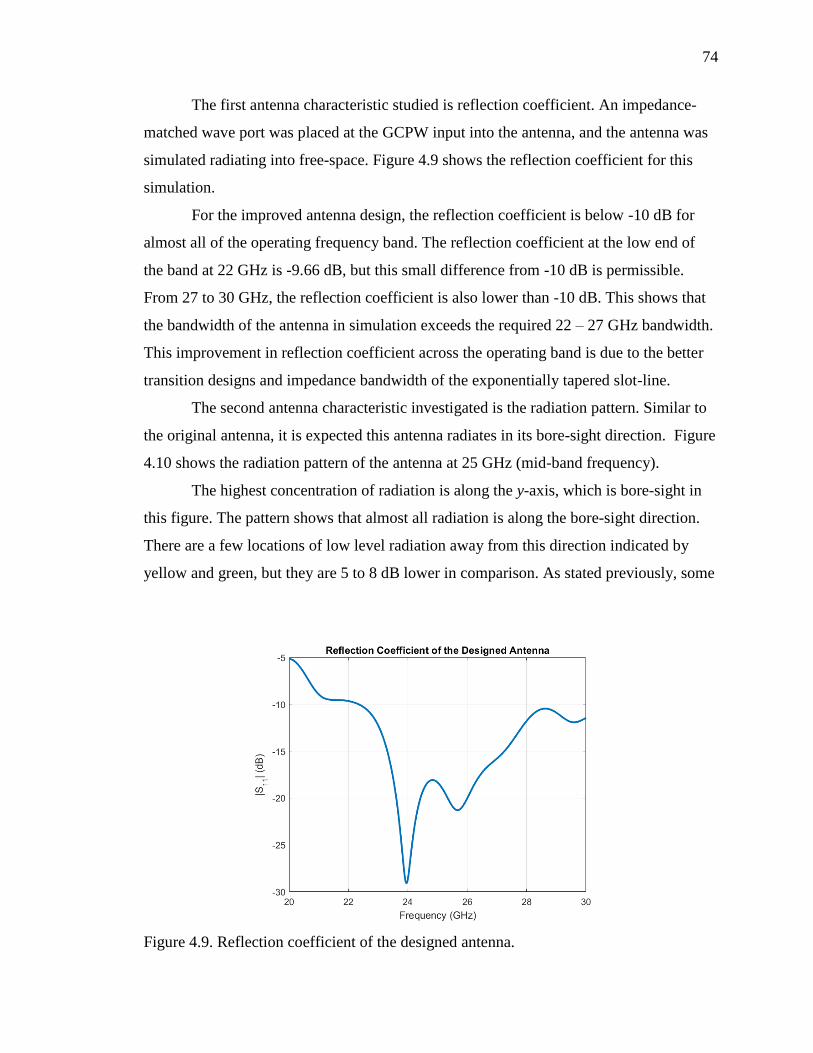
74
The first antenna characteristic studied is reflection coefficient. An impedance-
matched wave port was placed at the GCPW input into the antenna, and the antenna was
simulated radiating into free-space. Figure 4.9 shows the reflection coefficient for this
simulation.
For the improved antenna design, the reflection coefficient is below -10 dB for
almost all of the operating frequency band. The reflection coefficient at the low end of
the band at 22 GHz is -9.66 dB, but this small difference from -10 dB is permissible.
From 27 to 30 GHz, the reflection coefficient is also lower than -10 dB. This shows that
the bandwidth of the antenna in simulation exceeds the required 22 – 27 GHz bandwidth.
This improvement in reflection coefficient across the operating band is due to the better
transition designs and impedance bandwidth of the exponentially tapered slot-line.
The second antenna characteristic investigated is the radiation pattern. Similar to
the original antenna, it is expected this antenna radiates in its bore-sight direction. Figure
4.10 shows the radiation pattern of the antenna at 25 GHz (mid-band frequency).
The highest concentration of radiation is along the y-axis, which is bore-sight in
this figure. The pattern shows that almost all radiation is along the bore-sight direction.
There are a few locations of low level radiation away from this direction indicated by
yellow and green, but they are 5 to 8 dB lower in comparison. As stated previously, some
Figure 4.9. Reflection coefficient of the designed antenna.

75
Figure 4.10. Far-field radiation pattern of the designed antenna at 25 GHz.
radiation away from bore-sight can occur when there are slots disrupting surface current
flow on the antenna. These low level variations are potentially caused by this effect, but
the radiation in these directions is insignificant in comparison to bore-sight. Similar plots
at the other frequencies in the operating range show mostly similar radiation patterns
(Appendix D).
The final important antenna characteristic investigated is gain as a function of
frequency. This quantity was calculated in the same manner as the original antenna and is
shown in Figure 4.11. For the operating frequency range of 22 – 27 GHz, the gain varies
from 4 to 9 dB and increases with frequency. This is to be expected, since increasing gain
with frequency is the nature of this traveling wave antenna. At 22.5 GHz and 26.5 GHz,
the antennas has much lower gain. There are two possible reasons why the gain is lower
at these frequencies. The first reason is that the main radiation beam may drift off of the
bore-sight direction. Because CST® reports gain in the bore-sight direction, it is possible
that the gain is does not decrease, but the direction of maximum radiation is not bore-
sight. Figure 4.12 shows a comparison of the gain along the bore-sight direction and
maximum gain.
In this figure, the curve “Gain Along Bore-sight” refers to the same gain plotted
in Figure 4.11. The curve “Maximum Gain” refers to the maximum gain regardless of
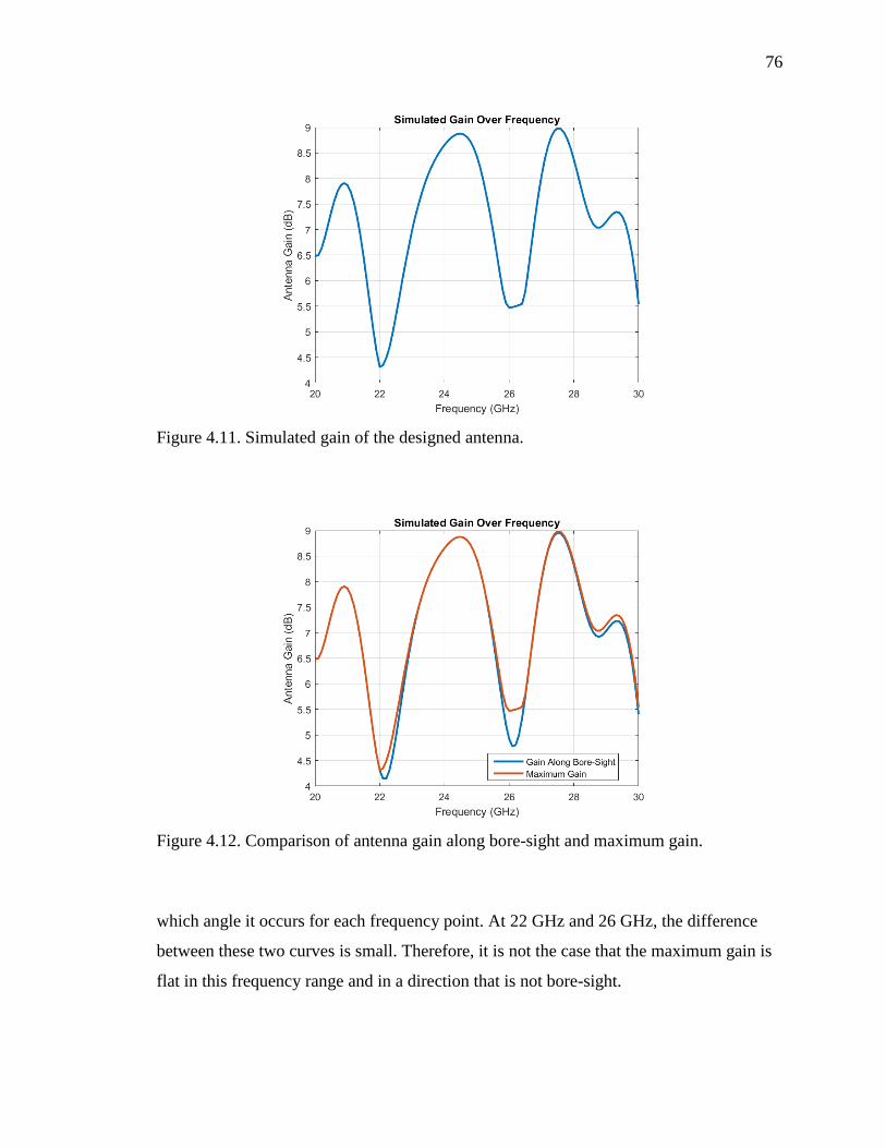
76
Figure 4.11. Simulated gain of the designed antenna.
Figure 4.12. Comparison of antenna gain along bore-sight and maximum gain.
which angle it occurs for each frequency point. At 22 GHz and 26 GHz, the difference
between these two curves is small. Therefore, it is not the case that the maximum gain is
flat in this frequency range and in a direction that is not bore-sight.

77
The second reason why the gain could be low is that efficiency losses dominate at
these two frequency ranges. If maximum gain and the gain along bore-sight are close in
value, then there must be some structure in the design that stores the microwave signals.
This would result in less power radiated and higher efficiency losses. For these two
frequency ranges, the antennas on each side in the three-element array act like resonant
structures, which store microwave signals preventing them from radiating out into free
space. Figure 4.13 shows the surface currents on one of the side antennas at 26 GHz.
In this figure, surface currents are plotted for one of the side antennas. The inputs to the
side antennas are terminated in open-circuits in simulation to simulate the reflective
property of the Hittite SP4T switch used in the linear array design. Because the inputs are
terminated in open-circuits, surface current standing waves are set up between the
terminated inputs and radiating ends of the side antennas shown in Figure 4.13. It is in
these standing waves at these two frequency ranges that the energy is stored and not
radiated. Because the standing waves are a function of the reflection coefficient at the
inputs of the side antennas, lower reflection coefficients reduce the efficiency losses. The
actual Hittite SP4T switch has a -5 dB reflection coefficient when switch is off, so the
efficiency losses would be lower if this antenna were to be used in a 1D array. Overall,
Figure 4.13. Standing waves in the surface currents on one of the side antennas.

78
the improved antenna is fairly directive with moderate efficiency losses only at the
beginning and end of the operating band.
The final stage of the design of this antenna is the integration of two receivers on
the top layer of the antenna. With the goal of designing a tapered slot-line antenna whose
reflection coefficient is below -10 dB completed, the final stage was designing integrated
receivers that were maximally sensitive to reflected electric fields. The receivers also
could not adversely impact the reflection coefficient in the process of making them
maximally sensitive. The receivers were based on the original design with a few
modifications to meet this design goal. Like the original antenna, each receiver consists
of a Schottky diode and a pick-up antenna. Figure 4.14 shows the schematic of the
tapered slot-line antenna with integrated receivers, and Table 4.4 shows the associated
dimensions.
For this investigation, the same Skyworks SMS7621-060 Schottky diode was
used in fabrication, so it was again modeled as an equivalent series lumped impedance of
12 Ω, 0 H, and 0.18 pF. For each receiver, the terminals of the lumped impedance were
electrically connected to the terminals of the pick-up antenna. This is indicated by the
diode symbol shown in Figure 4.14.
The redesign of the integrated receivers for maximum reflected electric field
sensitivity was in the design of the pick-up antenna. The shape and size of the pick-up
Figure 4.14. Schematic of designed antenna with integrated receivers.

79
Table 4.4. Dimensions of the integrated receivers.
Parameter
Name
Value
(mm)
𝐵𝑤 0.630
𝐵𝑙 7.850
𝐻𝑟 0.500
𝐻𝑑 1.100
𝐷𝑣 0.500
antennas connected to the terminals of the Schottky diodes significantly affects the signal
levels picked up on the receivers. The original antenna used a bow-tie shape for the pick-
up antennas. Increasing the electrical length of the pick-up antennas increases the signal
level at the terminals of the receivers. However, simply making the bow-ties larger raises
the reflection coefficient of the tapered slot-line antenna, since the bow-ties extend over
the tapered slot-line producing reflections. Therefore, the pick-up antennas must be
designed to be electrically larger while being confined to the same area so as to not raise
reflection coefficient. This was accomplished by using the “half-circle” shape shown in
Figure 4.14. The basic shape used for the pick-up antennas is a dipole with the ends
terminated in large half-circle shapes. The perimeter of this shape is higher than the
perimeter of a bow-tie that has the same overall area. An additional feature of the half-
circle shape is the wider frequency response. Since the electrical length is longer, and
there are multiple turns along the perimeter, pick-up antennas using this shape are more
sensitive to a wider frequency range.
While the half-circle pick-up antennas were employed in the final design, two
other shapes were also considered for comparison. The first is the same bow-tie of the
original antenna, and the second is a basic dipole. These comparisons were made to show
the benefit of using electrically longer pick-up antennas. Figure 4.15 shows the three
pick-up antennas.
The bow-tie has the same dimensions of the one used in the original antenna. The
length of the bow-tie from left end to the right was 2.0 mm, and the angle made by each
side was 35°. The purpose of adding the bowtie was to investigate a tapered slot-line with
better reflection coefficient characteristics but with the same pick-up antennas from the

80
(a)
(b)
(c)
Figure 4.15. (a) Half-circle, (b) bow-tie, and (c) dipole shapes investigated in the design
of the integrated receivers.
original antenna. The dipole has the same length as the bow-tie, but it consists of two
0.127 mm wide printed traces with their ends rounded. The dipole was added for
comparison as a pick-up antenna shape that is electrically shorter than the bow-tie shape.
A second change with the addition of the integrated receivers is the bend in the
DC bias lines shown in Figure 4.14. The bias lines were angled upwards, so the lines
were equally spaced between microstrip feeds of two adjacent tapered slot-line antennas.
This was the final adjustment made for reducing the high frequency signals that were
coupled to the DC bias lines. One potential source of surface currents coupling signals to
the bias lines is the microstrip line used to feed the antenna. Bending the bias lines to be
equally spaced between two microstrip lines minimized the coupled signals to the bias
lines from both microstrip lines.

81
With the additions of two integrated receivers on the tapered slot-line antenna, it
was simulated for three cases, where each case corresponded to receivers with half-circle,
bow-tie, and dipole pick-up antennas. For each case, the antenna was simulated in the
same way as the base tapered slot-line antenna, and the reflection coefficient, radiation
pattern, and gain were analyzed for the three completed antennas. The simulated
reflection coefficients for the three cases are shown in Figure 4.16.
For all three cases, the reflection coefficients follow the response of the base
tapered slot-line antenna with no integrated receivers shown in Figure 4.9. All three pick-
up antennas are infinitesimal, so they should minimally affect the reflection coefficient of
the tapered slot-line antenna. Their contribution to a change in reflection coefficient
should be the slight increase in reflections with their presence at the radiation end of the
antenna. Additionally, the bias lines will also have some small influence on the reflection
coefficient. This is mostly the case for all three pick-up antennas. The bow-tie and dipole
closely follow the response with no integrated receivers. However, the use of half-circle
pick-up antennas in the integrated receivers raises the reflection coefficient from 24 GHz
to 30 GHz. The half-circle pick-up antennas are designed to be large and to be highly
sensitive to electric fields, so they produce the highest reflections at the radiating end of
Figure 4.16. Reflection coefficient of the designed antenna with integrated receivers.

82
the tapered slot-line antenna. For all cases, the reflection coefficient is below -10 dB for
the entire operating frequency band, which again fulfills the objective of designing a
tapered slot-line antenna with a lower reflection coefficient.
Next, the addition of integrated receivers was investigated for their influence on
radiation characteristics. Figure 4.17 shows the far-field radiation pattern at 25 GHz for
the case of the half-circle pick-up antennas. For the two other cases, their radiation
patterns are identical.
For this figure, it is clear that the integrated receivers have little effect on the
direction of radiation. Here, all the radiation is still in the bore-sight direction as indicated
by the dark red color. Low level radiation is seen off of bore-sight as shown as yellow
and green, but they are 5 dB to 8 dB lower. Radiation plots at different frequencies across
the operating band have mostly similar characteristics (Appendix D).
Finally, the antenna gain over frequency was analyzed for the three pick-up
antenna cases and is shown in Figure 4.18. The antenna gain with integrated receivers is
similar for all three cases in the operating frequency band and closely follow the response
set by the base tapered slot-line antenna. The only difference is with the half-circle case
where the gain is lower, but this only occurs outside of the operating frequency range.
Figure 4.17. Far-field radiation of the designed antenna with integrated receivers using
half-circle pick-up antennas at 25 GHz.

83
Figure 4.18. Simulated gain for the three pick-up antenna cases.
The gain is in the 3 – 9 dB range and increases with frequency. Overall, the integrated
receivers with three different pick-up antenna shapes have minimal effect on gain. These
results show the integration of two receivers with different pick-up antenna shapes have
minimal effect on antenna characteristics.
The next analysis is on the sensitivity of each pick-up antenna shape to electric
fields. It is here where the three cases contrast greatly in terms of pick-up antenna
voltages. Figure 4.19 shows the difference in received voltages for the three different
pick-up antenna shapes. These values correspond to the microwave voltages across the
terminals of the pick-up antennas.
For each case, “1” and “2” refer to the top and bottom pick-up antennas from
Figure 4.14. The bow-ties and the dipoles have voltage responses ranging from 0.25 V to
1 V. In comparison, the half-circle pick-up antennas have higher responses ranging from
1 V to 1.5 V. The fluctuation at 24 GHz is due to the resonant frequency response of the
pick-up antennas. With the 0.9 V to 1.4 V response of the bow-ties on the original
antenna, the half-circle pick-up antennas have a higher response that increases with
frequency. While the increase with frequency is not ideal, the higher sensitivity at higher
frequencies improves the images produced by SAR algorithms. However, there is an
additional requirement for equalizing scan data acquired with this antenna during a

84
Figure 4.19. Simulated diode terminal voltages of the integrated receivers for three
different pick-up antenna shapes.
physical scan. Much like the equalization matrix from Section 3, variations in voltage
response as a function of frequency must be taken out when generating images with these
voltages. With the increased voltages at the terminals of the half-circle shapes, the second
goal of designing integrated receivers with higher sensitivity was accomplished.
Similar to the analysis of the original antenna, the electric fields radiating a short
distance away from the antenna were plotted to determine the beamwidth of radiated
electric fields close to the antenna. With respect to SAR, beamwidth is an important
antenna characteristic, since it determines the area irradiated during a scan. Because the
three cases for different pick-up antenna shapes have similar radiation characteristics, the
electric field distribution was only plotted for the half-circle case. The electric field
distribution is plotted from the antenna input to 32 mm in front of the radiating end at 25
GHz for two different perspectives in Figure 4.20 and Figure 4.21.
In Figure 4.20, the electric field is seen traveling down the tapered slot-line and
radiating out into air. For this perspective of seeing the electric field distribution from
above the antenna, the bore-sight direction is a horizontal vector moving to the right.
Much like the original antenna, the electric fields indicate high intensity along bore-sight

85
Figure 4.20. Electric field distribution at 25 GHz for the top view of the antenna.
Figure 4.21. Electric field distribution at 25 GHz for the bore-sight view of the antenna.
and lower intensity away from bore-sight. This indicates gain along the bore-sight
direction.
From the perspective of looking into the radiating end of the antenna and focused
32 mm away, this antenna has a wide beam similar to that for the original antenna. The
solid green circle a wide beam of radiation, where the edges of the beam are shown in
blue. Similar to the original antenna, the change from green to blue is approximately 30
dB. The fields mapped at other frequencies within the operating band show similar
electric field distributions (Appendix D). It is shown that the electric field radiated from
the improved antenna with integrated receivers are similar to the electric fields radiated
by the original antenna and are sufficient for SAR imaging.

86
With the analysis of the antenna with integrated receivers complete, this antenna
design improves reflection coefficient for the operating frequency band. From the
analysis of the radiation pattern and gain, the shape of the pick-up antennas have little
influence of the radiation characteristics of the antenna, but they increase the voltage
output of the integrated receivers. Better reflection coefficient and higher receiver voltage
output result in better SAR images.
4.2. PHYSICAL LAYOUT
The model of the improved antenna was exported from CST® and drafted in
Cadence Allegro PCB Editor. There were three antennas made for the three pick-up
antenna shapes. Figure 4.22. shows one of the assembled antennas with half-circle pick-
up antennas. Each antenna had a similar matched antenna on each side for comparison to
simulation. The result was three three-element arrays, where each three-element array
had a different pick-up antenna shape. The term “manufactured antenna” used in the
discussion of measurement results refers to a three-element array of fabricated antennas.
For all antennas, 100 Ω 0201 size choke resistors were placed on the DC bias lines to
attenuate high frequency signals on the lines. Additionally, low pass filters were soldered
at the end of the DC bias lines at the connector. Each low pass filter was formed by a
parallel 10 pF capacitor and 10 kΩ resistor combination. The Skyworks SMS7621-060
(a) (b)
Figure 4.22. (a) Top and (b) bottom view of the fabricated antenna with half-circle
shapes.

87
Schottky diodes were soldered to the terminals of the pick-up antennas. They were
soldered in the same configuration as the original antenna, so that one bias line outputs a
positive voltage, and the other outputs a negative voltage. The SMA connector from the
original antenna was switched to a K-connector shown in Figure 4.22. Metal posts were
soldered to the 0.100” pitch through-hole connector holes for connecting the output
voltages of both receivers to a data acquisition circuit.
4.3. ANTENNA MEASUREMENT
The manufactured antennas were first tested for their reflection coefficient
characteristics for comparison to simulation results shown previously. Figure 4.23 shows
the comparison of measured reflection coefficients to simulation for the three
manufactured antennas.
Measurement of reflection coefficient for the three manufactured antennas used
the same test setup for the original antenna. One at a time, the antennas were connected to
a coaxial port of the Anritsu Vector Star MS4644A vector network analyzer (VNA)
through a coaxial cable. The coaxial cable was calibrated to the cable end that connected
to each antenna. The VNA was set to transmit a wideband (20 – 30 GHz) signal into each
antenna, where it was held radiating into free-space. For the antenna with half-circles, the
measurement follows the frequency response from simulation but approximately -5 dB to
-10 dB lower in some areas. This difference is likely due to losses within the antenna.
From 20 to 22 GHz, the reflection coefficient is higher than – 10dB, but that range is
outside of the operating band. For the antenna with bow-ties, the measurement is much
lower at approximately 25.5 GHz. This behavior is likely due to a shift in the resonances
around 24 GHz moving higher in frequency for measurement. For this case, the shift in
frequency comes from the extra electrical length added by the connector on the antenna.
Finally, for the antenna with dipoles, the measurement follows simulation with some
resonances shifted higher in frequency. However, the reflection coefficient from 22 to
22.5 GHz around -7.5 dB. This high reflection coefficient is most likely due to reflections
at the precision connector used. Precision SMA connectors have a more difficult
procedure for bonding them to a PCB. In this case, the center pin of the connector was
slightly misaligned from the signal line of the GCPW, so it is possible that this connector

88
(a)
(b)
(c)
Figure 4.23. Comparison of measured reflection coefficients for the designed antenna to
simulation for: (a) half-circle, (b) bow-tie, and (c) dipole pick-up antennas.

89
caused these reflections. Additionally, the dipole shape can produce reflections at the
radiating end of the antenna that raise the reflection coefficient for low frequencies.
Overall, these three antennas have sufficiently low (-10 dB) reflection coefficients for
their operating frequency band.
Next, the antenna gain was measured for the antenna with half-circles. Since this
procedure requires precise antenna alignment and distance measurements and is time
consuming, and the gain and radiation patterns for the three simulation cases were mostly
the same, gain measurements were only made on the antenna with half-circles. The
overall measurement procedure followed that of the original antenna using the same test
setup. Gain was found using the Friis transmission formula and 𝑆21 measurements with
the VNA. The only difference was that since only one manufactured antenna was made
for each case, there were no two like antennas to use as the transmitter and receiver.
While the three manufactured antennas are similar in simulation and either the antenna
with the dipole or the bow-tie would probably have worked as the second antenna, a K-
band open-ended rectangular waveguide (OERW) was used instead for the second
antenna. The gain of the K-band OERW was known and experimentally verified prior to
performing the 𝑆21 measurement with the manufactured antenna with half-circles.
Experimental verification was simply making gain measurements of the OERW with 𝑆21
measurements and the Friis transmission formula. The gain of the OERW ranged from 3
dB to 6 dB and increased with frequency. For the gain measurement with the
manufactured antenna, the antenna and OERW were aligned pointing at each other in
their respective directions of maximum radiation. For averaging, the distance between the
antennas was changed from 200 mm to 220 mm in 2 mm increments. These distances
were factored into the transmission formula, and the calculated gain measurements were
averaged. Figure 4.24 shows the measured gain over frequency.
The measured gain is slightly lower and fluctuates less across the frequency band
in comparison to the simulation. Because the antennas on the sides in the three-element
array have inputs terminated in matched loads, they do not resonate like in simulation.
Therefore, they do not have the same fluctuations. Additionally, the lower gain can be
attributed to efficiency losses in the physical antenna that drive down the gain. The
reported gain at 28 – 30 GHz is not reliable due to the transmitting waveguide not
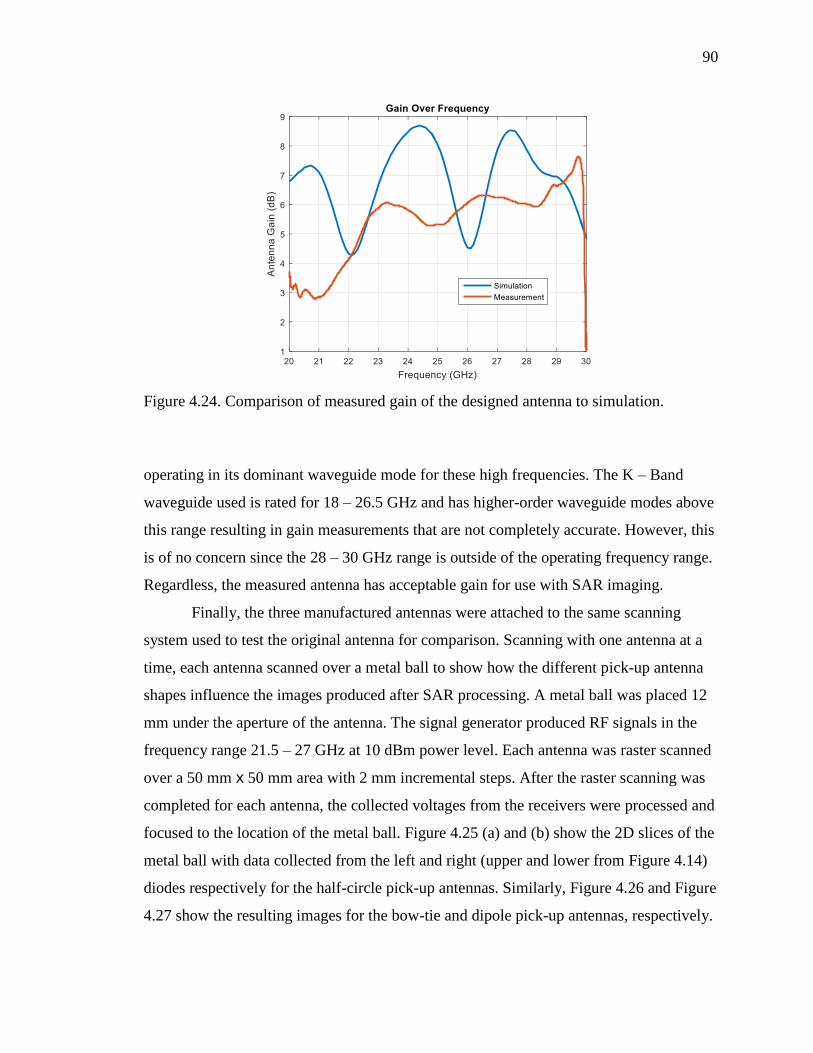
90
Figure 4.24. Comparison of measured gain of the designed antenna to simulation.
operating in its dominant waveguide mode for these high frequencies. The K – Band
waveguide used is rated for 18 – 26.5 GHz and has higher-order waveguide modes above
this range resulting in gain measurements that are not completely accurate. However, this
is of no concern since the 28 – 30 GHz range is outside of the operating frequency range.
Regardless, the measured antenna has acceptable gain for use with SAR imaging.
Finally, the three manufactured antennas were attached to the same scanning
system used to test the original antenna for comparison. Scanning with one antenna at a
time, each antenna scanned over a metal ball to show how the different pick-up antenna
shapes influence the images produced after SAR processing. A metal ball was placed 12
mm under the aperture of the antenna. The signal generator produced RF signals in the
frequency range 21.5 – 27 GHz at 10 dBm power level. Each antenna was raster scanned
over a 50 mm x 50 mm area with 2 mm incremental steps. After the raster scanning was
completed for each antenna, the collected voltages from the receivers were processed and
focused to the location of the metal ball. Figure 4.25 (a) and (b) show the 2D slices of the
metal ball with data collected from the left and right (upper and lower from Figure 4.14)
diodes respectively for the half-circle pick-up antennas. Similarly, Figure 4.26 and Figure
4.27 show the resulting images for the bow-tie and dipole pick-up antennas, respectively.

91
(a) (b)
Figure 4.25. Images generated with: (a) left diode and (b) right diode for the half-circle
pick-up antennas.
(a) (b)
Figure 4.26. Images generated with: (a) left diode and (b) right diode for the bow-tie
pick-up antennas.
(a) (b)
Figure 4.27. Images generated with: (a) left diode and (b) right diode for the dipole pick-
up antennas.
X (mm)
Y (
mm
)
Board 1, Channel A
0 20 400
20
40
5
10
15
20
X (mm)
Y (
mm
)
Board 1, Channel B
0 20 40
10
20
30
40
50
50
100
150
200
X (mm)
Y (
mm
)
Board 1, Channel A
0 20 400
20
40
2
4
6
8
10
X (mm)
Y (
mm
)
Board 1, Channel B
0 20 40
10
20
30
40
50
20
40
60
80
100
X (mm)
Y (
mm
)
Board 1, Channel A
0 20 400
20
40
2
4
6
8
10
X (mm)
Y (
mm
)
Board 1, Channel B
0 20 40
10
20
30
40
50
20
40
60
80

92
The images of the metal ball for the half-circle case show higher intensity over the
target with low noise around the target. Additionally, the metal ball is round in these
images. In comparison, the images for the bow-tie and dipole cases show distorted
representations of the metal ball with significant noise surrounding the target. The metal
ball in each figure is in a slightly different X and Y location. Each antenna was mounted
to a scanning frame and approximately centered over the metal ball, so some slight
location variations can exist. The variation in location between the receivers for each case
is due to the receivers being at different locations with respect to the metal ball. By
comparing the images with the half-circle pick-up antennas vs bow-ties and dipoles, it is
shown that there is a benefit to having high sensitivity across all frequencies in the
operating frequency range.
The results shown in this section show how the tapered slot-line designed for the
imaging system can be improved for better imaging capabilities. With the same overall
antenna size and components used as the original antenna, antenna characteristics were
improved with a few key modifications to design.

93
5. SUMMARY
A linear imaging system operating from 22 GHz to 27 GHz was developed for
creating microwave images of large areas in a short period of time. The final design
consisted of two linear arrays and one controller board. Each linear array was composed
of 16 tapered slot-line antennas with receivers having non-uniform spacing mounted at
the radiating end of the array. The controller board housed the transmitting and data
acquisition circuitry necessary for electronically scanning along the arrays. The imaging
system was mounted to a small mechanical scanning table for system testing.
The system’s performance was shown in the images generated for various targets.
Images showing detection of air voids in rubber were shown, which shows how the
system can be used for nondestructive evaluation. Images showing metal keys under
thick dielectric coating shows how the system can also be used for the detection of
contraband.
Further study in the design of the tapered slot-line antenna showed an improved
antenna with reflection coefficient lower than -10 dB for 22 – 27 GHz by redesigning the
shape of the antenna. The shape of the pick-up antenna was investigated for increasing
the voltage output of the two receivers mounted on each antenna. The half-circle shaped
pick-up antenna showed increased voltage response over the original antenna design.
Images generated with the improved antenna showed the benefit of having a lower
reflection coefficient and high receiver voltage output.

94
6. FUTURE WORK
The most fundamental expansion upon this work is manufacturing 16-element
linear arrays using the improved antenna with half-circle pick-up antennas. Imaging
results showing better image quality of a metal ball with the improved antennas means
the image system would benefit from this new antenna design. While the redesigned
antenna does not reduce image data acquisition time, the quality of the images produced
would be much better than the images produced by the current system.
Another important improvement that can be made for the system is having a
better equalization matrix for calibrating the receivers in the arrays. The equalization
matrix used in this system is a first order approximation for equalizing signals from all
receivers. A better equalization matrix could be constructed using the envelope of the
signals obtained from the moving metal plate experiment instead of using the mean of the
signals.
A final suggestion is the construction of a radome to cover the radiating ends of
the linear arrays. Adding a radome would add protection to the linear arrays when
handling the system and when the system scans over abrasive materials.

APPENDIX A
ORIGINAL ANTENNA DESIGN

96
Far-field radiation plots of the original antenna:
The far-field radiation plots for the original antenna without integrated receivers
are similar across the operating frequency band. At each frequency point, all radiation is
in the bore-sight direction and is in a wide beam. These plots are for the antenna without
integrated receivers and bias lines.
Far-field radiation plot at 20 GHz
Far-field radiation plot at 30 GHz

97
The far-field radiation plots have little change with the addition of integrated
receivers. With exception to 22 GHz, the far-field plots are fairly similar. These plots are
for the original antenna with integrated receivers and bias lines.
Far-field radiation plot at 20 GHz
Far-field radiation plot at 30 GHz
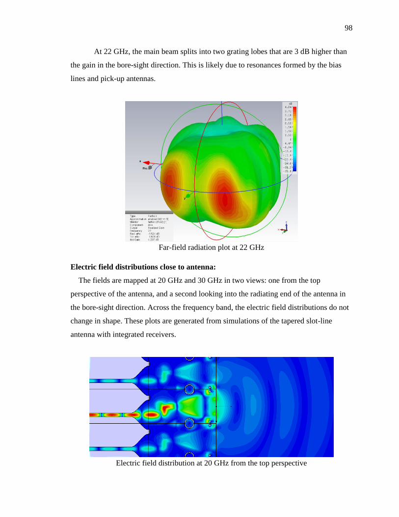
98
At 22 GHz, the main beam splits into two grating lobes that are 3 dB higher than
the gain in the bore-sight direction. This is likely due to resonances formed by the bias
lines and pick-up antennas.
Far-field radiation plot at 22 GHz
Electric field distributions close to antenna:
The fields are mapped at 20 GHz and 30 GHz in two views: one from the top
perspective of the antenna, and a second looking into the radiating end of the antenna in
the bore-sight direction. Across the frequency band, the electric field distributions do not
change in shape. These plots are generated from simulations of the tapered slot-line
antenna with integrated receivers.
Electric field distribution at 20 GHz from the top perspective

99
Electric field distribution at 30 GHz from the top perspective
Electric field distribution at 20 GHz looking into the radiating end of the antenna

100
Electric field distribution at 30 GHz looking into the radiating end of the antenna

APPENDIX B
LINEAR ARRAY DESIGN

102
Circuit schematics for the linear array board:
The circuit models for the linear array was designed in Design Entry CIS. The
schematics shown below follow the transmission of electric fields from the input
connector on the linear array to each antenna. Only one of the low level switch circuits is
shown, since all low level switch circuits had the same circuit model. A “O” indicates
signal input into the model, and a “X” indicates a signal flowing out of the model. The
element “2-PinConn” represents a connecting point between the linear array board and
daughter board.
Input connector to the linear array board followed by a Pi attenuator
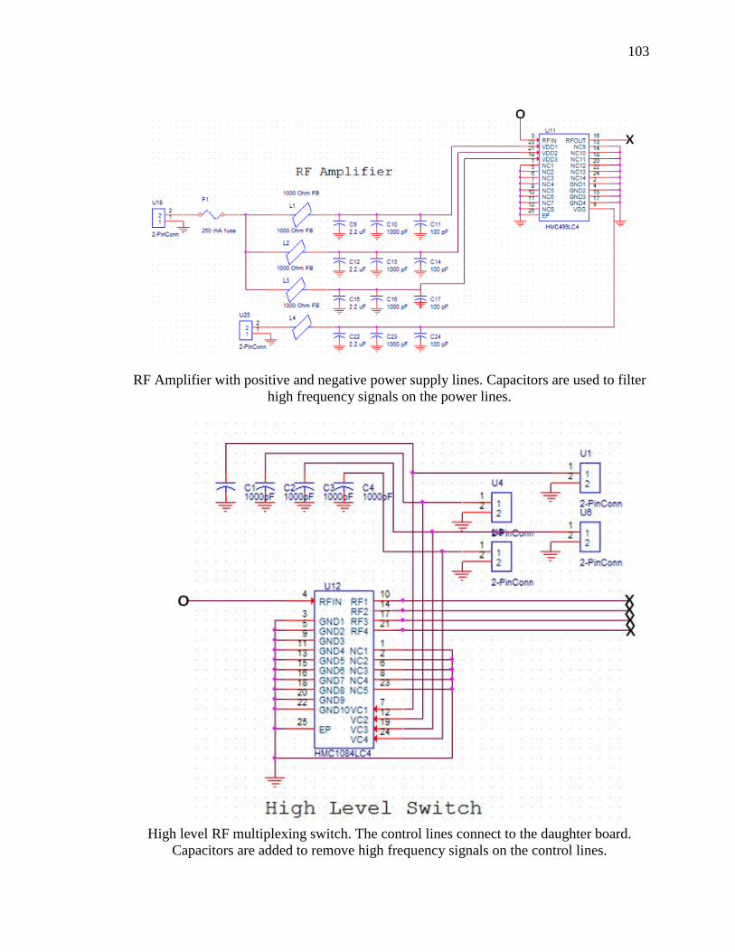
103
RF Amplifier with positive and negative power supply lines. Capacitors are used to filter
high frequency signals on the power lines.
High level RF multiplexing switch. The control lines connect to the daughter board.
Capacitors are added to remove high frequency signals on the control lines.

104
Low level RF multiplexing switch. The control lines connect to the daughter board.
Capacitors are added to remove high frequency signals on the control lines.
“Vivaldi_Antenna” represents the antenna in the array as a circuit element. The outputs
represent receiver voltage output lines. There are three additional low level switches with
similar circuit models.

105
Circuit schematics for the daughter board:
Several circuits were also designed to provide power and digital control for the
linear array board. These secondary circuits were designed on the daughter board.
Power sequencing circuit for the RF amplifier. The negative supply provides power to the
amplifier first then opens a switch for the positive supply to send power to the amplifier.
Regulators are added to fix the voltages on the amplifier power rails.
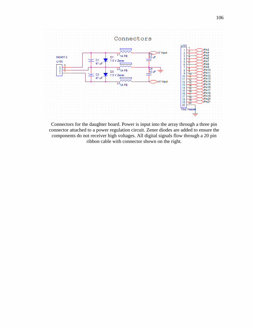
106
Connectors for the daughter board. Power is input into the array through a three pin
connector attached to a power regulation circuit. Zener diodes are added to ensure the
components do not receiver high voltages. All digital signals flow through a 20 pin
ribbon cable with connector shown on the right.

107
Inverter circuit for RF switches. Digital signals input into the array are first passed
through this inverter circuit that converts 0 to 3.3 V logic to 0 to -3.3 V logic. The voltage
regulator sets the output voltage level on the inverters. Output lines of the inverters are
directed to connector points for connection to the linear array board.
Receiver output voltage multiplexer circuit. Outputs from all antennas in the linear array
are connected to the different multiplexer chip. Voltages regulators set the rail-to-rail
voltages of the multiplexer.

108
PCB layouts of the linear array board and daughter board:
Both boards were designed in Cadence Allegro PCB Editor and assembled by Hughes
Circuits.
Linear array PCB layout
Daughter Board PCB layout

109
Electric field distributions of the linear array:
Simulations were made to show the electric fields propagating from an antenna in
the linear array. Plots made from these simulations show the beam width of the radiating
antenna. Across the operating frequency band, the radiation similar. The only differences
are the beam width changing as a function of antenna gain. At 23 GHz, the main beam is
much narrower than at 30 GHz. However, at 30 GHz, there exist side lobes around the
main beam.
Electric field distribution at 23 GHz

110
Electric field distribution at 30 GHz
Simulations were repeated for the linear array with metallic shield. Across the
operating frequency band, the radiation is similar in comparison to the plots of the array
without the metallic shield. The only difference is the higher radiation around the array
that is not in the main beam for 30 GHz. With the metallic shield, there are more side
lobes at the upper end of the frequency range.
Electric field distribution at 23 GHz

111
Electric field distribution at 30 GHz

APPENDIX C
CONTROLLER BOARD CIRCUIT MODELS

113
Circuit schematics for the controller board:
The controller board was designed as several modules, where each module
performed a specific task. These modules are shown below as self-contained circuits.
Controller board power input. A power protection circuit was made to ensure all
components could not receive high voltages. Capacitors were added to remove high
frequency signals from the external power supply.
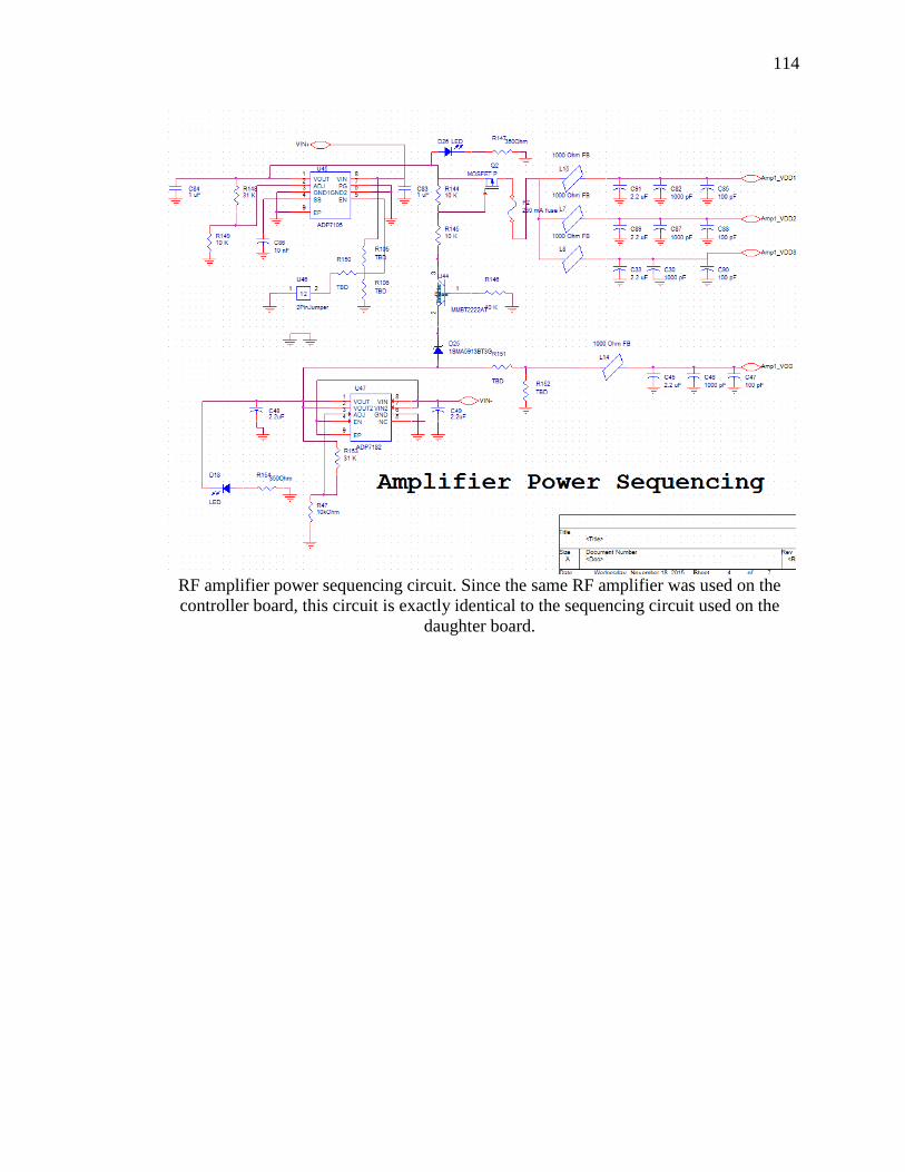
114
RF amplifier power sequencing circuit. Since the same RF amplifier was used on the
controller board, this circuit is exactly identical to the sequencing circuit used on the
daughter board.
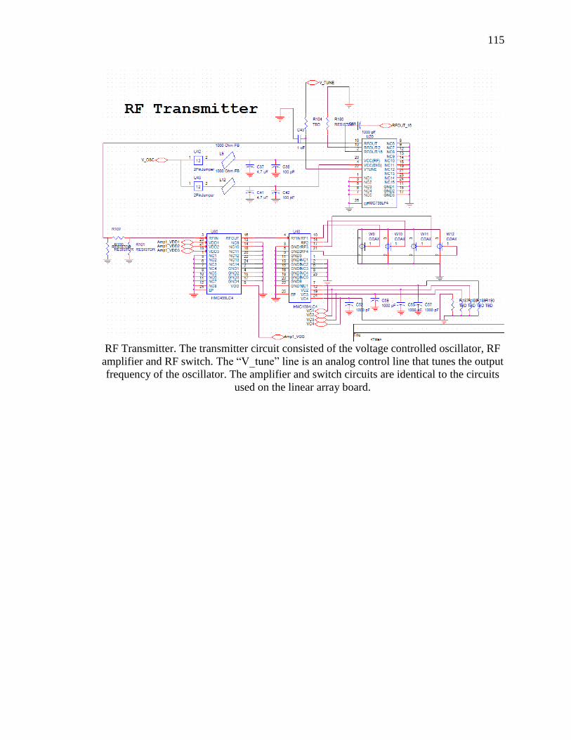
115
RF Transmitter. The transmitter circuit consisted of the voltage controlled oscillator, RF
amplifier and RF switch. The “V_tune” line is an analog control line that tunes the output
frequency of the oscillator. The amplifier and switch circuits are identical to the circuits
used on the linear array board.

116
Switch inverter circuit. The same inverter circuit was required for controlling the RF
switch on the controller board.
Controller board voltage regulators. All modules required specific, steady voltage. These
regulators are tuned to a specific voltage and remove high frequency signals.

117
ADC single to differential amplifiers. The positive and negative outputs from the antenna
receivers were individually referenced to ground. These amplifiers converted the outputs
into separate differential signals referenced to the ADC reference voltage before flowing
into the ADCs.
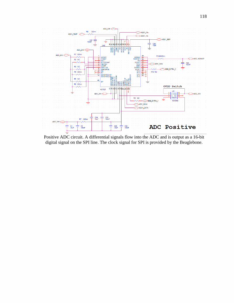
118
Positive ADC circuit. A differential signals flow into the ADC and is output as a 16-bit
digital signal on the SPI line. The clock signal for SPI is provided by the Beaglebone.

119
Negative ADC circuit. A differential signal flows into the ADC and is output as a 16-bit
digital signal on the SPI line. The clock signal for SPI is provided by the Beaglebone.

120
R2R ladder circuit. An 8-bit digital signal is passed through an R2R ladder and amplified
through the op-amp for tuning the voltage controlled oscillator.
Analog input switch. This low frequency switch was used to switch between the outputs
of the two linear arrays used in the final system.

121
Controller board PCB layout:
The controller board was also designed in Cadence Allegro Editor, and the board
was printed by Advanced Circuits. Components were installed in house.
Controller board PCB layout.

APPENDIX D
IMPROVED ANTENNA DESIGN

123
Far-field radiation plots of the improved antenna:
The far-field radiation plots for the improved antenna without integrated receivers
are similar across the operating frequency band. At each frequency point, all radiation is
in the bore-sight direction and is in a wide beam. At lower frequencies, the beam is fairly
broad, and the beam becomes narrower as the frequency increases. These plots are for the
antenna without integrated receivers and bias lines.
Far-field radiation plot at 22 GHz
Far-field radiation plot at 27 GHz

124
The far-field radiation plots have little change with the addition of integrated
receivers. Additionally, the main beam does not split at frequencies within the operating
band, unlike with the original antenna. These plots are for the original antenna with
integrated receivers and bias lines.
Far-field radiation plot at 22 GHz
Far-field radiation plot at 27 GHz

125
Electric field distributions close to antenna:
The fields are mapped at 22 GHz and 27 GHz in two views: one from the top
perspective of the antenna, and a second looking into the radiating end of the antenna in
the bore-sight direction. Across the frequency band, the electric field distributions do not
change in shape. These plots are generated from simulations of the tapered slot-line
antenna with integrated receivers.
Electric field distribution at 22 GHz from the top perspective
Electric field distribution at 27 GHz from the top perspective

126
Electric field distribution at 22 GHz looking into the radiating end of the antenna
Electric field distribution at 27 GHz looking into the radiating end of the antenna

127
BIBLIOGRAPHY
[1] D. M. Pozar, Microwave engineering, 3rd ed. Hoboken, NJ: J. Wiley, 2005.
[2] R. Zoughi, Microwave Non-Destructive Testing and Evaluation. The Netherlands:
Kluwer, 2000.
[3] P. J. Shull, Nondestructive Evaluation: Theory, Techniques, and Applications.
New York: Marcel Dekker, 2002.
[4] Y. Chin-Yung and Z. Reza, "A novel microwave method for detection of long
surface cracks in metals," IEEE Transactions on Instrumentation and
Measurement, vol. 43, pp. 719-725, 1994.
[5] C. Huber, H. Abiri, S. I. Ganchev, and R. Zoughi, "Modeling of surface hairline-
crack detection in metals under coatings using an open-ended rectangular
waveguide," IEEE Transactions on Microwave Theory and Techniques, vol. 45,
pp. 2049-2057, 1997.
[6] M. T. Ghasr, S. Kharkovsky, R. Zoughi, and R. Austin, "Comparison of near-field
millimeter-wave probes for detecting corrosion precursor pitting under paint,"
IEEE Transactions on Instrumentation and Measurement, vol. 54, pp. 1497-1504,
2005.
[7] S. Kharkovsky, J. T. Case, M. A. Abou-Khousa, R. Zoughi, and F. L. Hepburn,
"Millimeter-wave detection of localized anomalies in the space shuttle external
fuel tank insulating foam," IEEE Transactions on Instrumentation and
Measurement, vol. 55, pp. 1250-1257, 2006.
[8] S. Kharkovsky and R. Zoughi, "Microwave and millimeter wave nondestructive
testing and evaluation - Overview and recent advances," IEEE Instrumentation &
Measurement Magazine, vol. 10, pp. 26-38, 2007.
[9] G. Zheng, R. Zhang, S. Li, P. He, H. Zhou, and Y. Shi, "A Hyperlens-Embedded
Solid Immersion Lens for Beam Focusing Beyond the Diffraction Limit," IEEE
Photonics Technology Letters, vol. 23, pp. 1234-1236, 2011.
[10] J. T. Case, "Microwave and millimeter wave imaging using synthetic aperture
focusing and holographical techniques," MS thesis, ECE Dept., MST Univ.,
Rolla, MO, 2005.
[11] United States. Columbia Accident Investigation Board. and H. W. Gehman,
Columbia Accident Investigation Board : report. Arlington, Va. Washington,
D.C.: Columbia Accident Investigation Board ; Distributed by National
Aeronautics and Space Administration, 2003.

128
[12] S. Kharkovsky, F. L. Hepburn, J. Walker, and R. Zoughi, "Testing of the space
shuttle external fuel tank SOFI using near-field and focused millimeter wave
nondestructive testing techniques," Materials Evaluation, vol. 63, pp. 516-522,
May 2005 2005.
[13] J. T. Case, F. L. Hepburn, and R. Zoughi, "Inspection of Spray on Foam
Insulation (SOFI) Using Microwave and Millimeter Wave Synthetic Aperture
Focusing and Holography," in Instrumentation and Measurement Technology
Conference, 2006. IMTC 2006. Proceedings of the IEEE, 2006, pp. 2148-2153.
[14] J. T. Case, M. T. Ghasr, and R. Zoughi, "Optimum Two-Dimensional Uniform
Spatial Sampling for Microwave SAR-Based NDE Imaging Systems," IEEE
Transactions on Instrumentation and Measurement, vol. 60, pp. 3806-3815, 2011.
[15] M. T. Ghasr, J. T. Case, and R. Zoughi, "Novel Reflectometer for Millimeter-
Wave 3-D Holographic Imaging," IEEE Transactions on Instrumentation and
Measurement, vol. 63, pp. 1328-1336, 2014.
[16] D. M. Sheen, D. L. McMakin, and T. E. Hall, "Three-dimensional millimeter-
wave imaging for concealed weapon detection," IEEE Transactions on
Microwave Theory and Techniques, vol. 49, pp. 1581-1592, 2001.
[17] M. T. Ghasr, M. A. Abou-Khousa, S. Kharkovsky, R. Zoughi, and D.
Pommerenke, "Portable Real-Time Microwave Camera at 24 GHz," IEEE
Transactions on Antennas and Propagation, vol. 60, pp. 1114-1125, 2012.
[18] TSA: Advanced Imaging Technology (AIT). Available:
http://www.tsa.gov/approach/tech/ait/index.shtm.
[19] P. Mehta, K. Chand, D. Narayanswamy, D. G. Beetner, R. Zoughi, and W. V.
Stoecker, "Microwave reflectometry as a novel diagnostic tool for detection of
skin cancers," IEEE Transactions on Instrumentation and Measurement, vol. 55,
pp. 1309-1316, 2006.
[20] T. M. Grzegorczyk, P. M. Meaney, P. A. Kaufman, R. M. diFlorio-Alexander,
and K. D. Paulsen, "Fast 3-D Tomographic Microwave Imaging for Breast Cancer
Detection," IEEE Transactions on Medical Imaging, vol. 31, pp. 1584-1592,
2012.
[21] M. A. Abou-Khousa, M. T. Ghasr, S. Kharkovsky, D. Pommerenke, and R.
Zoughi, "Modulated Elliptical Slot Antenna for Electric Field Mapping and
Microwave Imaging," IEEE Transactions on Antennas and Propagation, vol. 59,
pp. 733-741, 2011.

129
[22] M. T. Ghasr, M. A. Abou-Khousa, S. Kharkovsky, R. Zoughi, and D.
Pommerenke, "A Novel 24 GHz One-Shot, Rapid and Portable Microwave
Imaging System," in Instrumentation and Measurement Technology Conference
Proceedings, 2008. IMTC 2008. IEEE, 2008, pp. 1798-1802.
[23] M. T. Ghasr, S. Kharkovsky, R. Bohnert, B. Hirst, and R. Zoughi, "30 GHz
Linear High-Resolution and Rapid Millimeter Wave Imaging System for NDE,"
IEEE Transactions on Antennas and Propagation, vol. 61, pp. 4733-4740, 2013.
[24] S. Kharkovsky, M. T. Ghasr, K. Kam, R. Zoughi, and M. A. Abou-Khousa,
"Microwave resonant out-of-plane fed elliptical slot antenna for imaging
applications," in Instrumentation and Measurement Technology Conference
(I2MTC), 2011 IEEE, 2011, pp. 1-4.
[25] M. A. Baumgartner, M. T. Ghasr, and R. Zoughi, "Wideband Imaging Array
Using Orthogonally Fed Dual Varactor-Loaded Elliptical Slots," IEEE
Transactions on Instrumentation and Measurement, vol. 64, pp. 740-749, 2015.
[26] Rogers, "RO4003, RO4350 High Frequency Laminates," ed, 1999, p. 4.
[27] C. A. Balanis, Antenna theory : analysis and design, 3rd ed. Hoboken, NJ: John
Wiley, 2005.
[28] Skyworks, "Surface Mount Mixer and Detector Schottky Diodes," ed, 2015.
[29] Hititte Microwave Products, "HMC499LC4," ed, p. 8.
[30] Hititte Microwave Products , "HMC1084LC4," ed, p. 8.
[31] "ADG726/ADG732," ed: Analog Devices.
[32] G. Coley, "BeagleBone Black System Reference Manual," A5.2 ed.
[33] Texas Instruments, "AM355x Sitara Processors," ed.
[34] Analog Devices, "AD7621," ed, 2005, p. 32.
[35] Hititte Microwave Products , "HMC739LP4," ed, p. 8.
[36] K. Ebnabbasi, D. Busuioc, R. Birken, and M. Wang, "Taper Design of Vivaldi
and Co-Planar Tapered Slot Antenna (TSA) by Chebyshev Transformer," IEEE
Transactions on Antennas and Propagation, vol. 60, pp. 2252-2259, 2012.
[37] Z. Wen Xun, "Extended study on tapered slot-line antennas," in Advanced
Technologies for Communications (ATC), 2012 International Conference on,
2012, pp. 50-54.

130
VITA
Matthew Jared Horst was born on February 5, 1992 in St. Louis, Missouri. He
attended Southeast Missouri State University in Fall 2010 for a pre-engineering program.
In Fall 2012, he transferred to Missouri University of Science and Technology (Missouri
S&T) for a Bachelor’s degree in Electrical Engineering. While attending Missouri S&T,
he was hired as an undergraduate research assistant at the Applied Microwave
Nondestructive Testing Laboratory (amntl). He graduated from Missouri S&T in
December 2014 with the degree in Electrical Engineering.
In January 2015, he began a Master’s degree program in Electrical Engineering
with amntl at Missouri S&T. In April 2015, he was award the National Science
Foundation Graduate Research Fellowship for pursuing a Master’s degree. Matt
completed his Master’s of Science in Electrical Engineering in July 2016.
Recommended