ECE 4430
Project 2: Design of Operational
AmplifierStudent 1: Moez Karim Aziz
Student 2: Hanbin (Victor) Ying
12/6/2016
I have neither given nor received any unauthorized assistance on this project.
2
Design Summary
• Design Environment: Cadence Virtuosos, LTSpice, ADS
• Technology: Baker’s 50nm CMOS process
• Supply: 1 V
• Topology:
Folded cascode differential amplifier + push-pull output stage

3
Schematic of Op-Amp
PMOS Diff PairDiff Pair Summing &
Floating Current SourcePush Pull
output
I4 = 9.243 uA
Reference: R. Jacob Baker. 2010. CMOS Circuit Design, Layout, and Simulation (3rd ed.). Wiley-IEEE Press
I3 = 9.224 uA
I2 = 3.27 uA
I1 = 15.3 uA
I6 = 15.2 uAI5 = 15.3uA
Iout = 60.31uA
NMOS Diff Pair
Note: DC current under loaded, zero AC input
condition with common-mode voltage of 500 mV.

4
Design Process—Diff Pairs
• M5 and M14 represent the tail current source of the PMOS diff pair, and M15 and
M10 represent the tail current source of the NMOS diff pair. To reduce the overdrive
voltage of these transistors so as to increase ICMR, W/L’s of these four transistors
were made large with the constraint that the tail current should avoid excessive
power consumption.
• M2, M3, M4, and M9 represent the input transistors of the two diff pairs. Therefore,
to obtain large CMRR, the W/L’s of these four transistors were maximized to reduce
vgs for a given vin. In addition, the tail current is sized to keep these four transistors in
saturation.
• Length of M5, M14, and M15 (tail current source transistors) increased beyond
2*minimum feature size to mitigate channel-length modulation and increase output
resistance with constraints of keeping tail current high and occupying small chip
area.
• While diff gain is mostly determined by the diff pair, the common mode gain is found
to be affected by every transistor in the summing circuit.
5
Design Process—Summing Circuit
• Recognize that transistors M20, M21, M59, and M60 form a PMOS folded cascode
current mirror and that transistors M22, M23, M63, and M62 form an NMOS folded
cascode current mirror. Therefore, the dimensions of M20 and M59 should be equal,
as should the dimensions of M21 and M60, M22 and M63, and M23 and M62.
• To form an effective current mirror, channel-length modulation needs to be as
mitigated as possible, meaning that length of each transistor should be reasonably
large. At the same time, length must be kept sufficiently small so as to keep a
sufficiently high W/L to maintain appropriate voltage biasing.
• Recall that since length is inversely proportional to λ (channel-length modulation
constant) and that since ro ∝1
λ𝐼𝐷, a larger length tends to make ro larger. A larger ro
enables small-signal changes in one branch of the summing circuit to be mirrored
more accurately.
• Because the slew rate is affected mainly by the output buffer and floating current
source, the main cascode branch is sized to conduct minimal current, which reduces
the power consumption.
6
Design Process—Output Stage
• Chose push-pull topology with output transistors (M70 and M71) as well as floating
current source transistors (M66-M69) because:
o Rload is large, so its effect on gain degradation is minimal.
o The topology has high power efficiency.
o The topology is capable of wide output swing.
• From slew rate (SR) and loading specifications, output current should be:
IOUT, MINIMUM = SR*Cload = (40*106 V/s)*(10-12 F)=40uA
• The W/L ratios of transistors M66-M69 were tuned such that their VDS values, i.e.,
the floating battery voltages, biased the output stage on the verge of turning on. This
reduces the quiescent power consumption while still satisfying the slew rate
requirement.
• The floating current source transistors are placed on both sides of the main cascode
summing circuit to minimize input referred offset voltage.
• Capacitive compensation (C0 and C7) are employed to provide phase margin. Two
compensation caps are found to provide better large signal response than one cap.
7
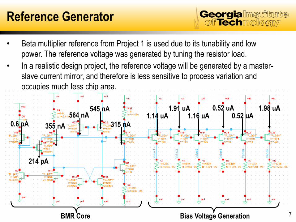
Reference Generator
• Beta multiplier reference from Project 1 is used due to its tunability and low
power. The reference voltage was generated by tuning the resistor load.
• In a realistic design project, the reference voltage will be generated by a master-
slave current mirror, and therefore is less sensitive to process variation and
occupies much less chip area.
Bias Voltage GenerationBMR Core
1.98 uA0.52 uA
0.52 uA1.16 uA
1.91 uA1.14 uA
315 nA
545 nA564 nA
355 nA0.6 pA
214 pA
8
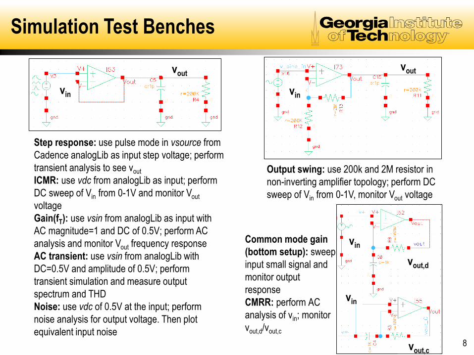
Simulation Test Benches
Common mode gain
(bottom setup): sweep
input small signal and
monitor output
response
CMRR: perform AC
analysis of vin; monitor
vout,d/vout,c
Step response: use pulse mode in vsource from
Cadence analogLib as input step voltage; perform
transient analysis to see vout
ICMR: use vdc from analogLib as input; perform
DC sweep of Vin from 0-1V and monitor Vout
voltage
Gain(fT): use vsin from analogLib as input with
AC magnitude=1 and DC of 0.5V; perform AC
analysis and monitor Vout frequency response
AC transient: use vsin from analogLib with
DC=0.5V and amplitude of 0.5V; perform
transient simulation and measure output
spectrum and THD
Noise: use vdc of 0.5V at the input; perform
noise analysis for output voltage. Then plot
equivalent input noise
Output swing: use 200k and 2M resistor in
non-inverting amplifier topology; perform DC
sweep of Vin from 0-1V, monitor Vout voltage
vout
vin
vout
vin
vin
vin
vout,d
vout,c
9
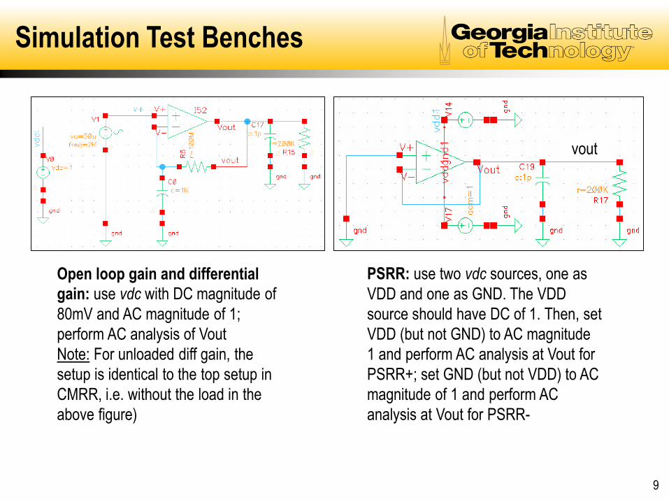
Simulation Test Benches
PSRR: use two vdc sources, one as
VDD and one as GND. The VDD
source should have DC of 1. Then, set
VDD (but not GND) to AC magnitude
1 and perform AC analysis at Vout for
PSRR+; set GND (but not VDD) to AC
magnitude of 1 and perform AC
analysis at Vout for PSRR-
Open loop gain and differential
gain: use vdc with DC magnitude of
80mV and AC magnitude of 1;
perform AC analysis of Vout
Note: For unloaded diff gain, the
setup is identical to the top setup in
CMRR, i.e. without the load in the
above figure)
vout
10
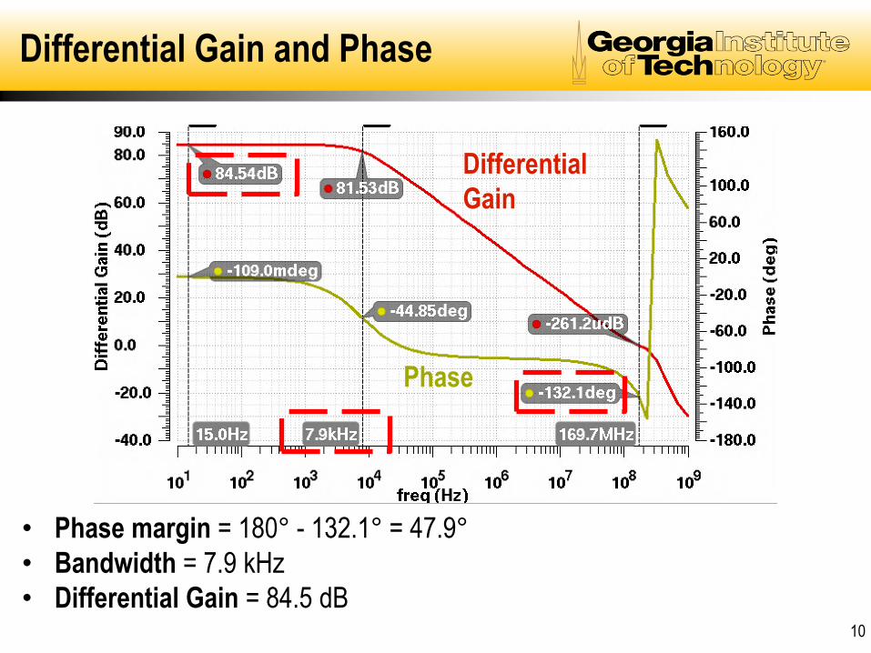
Differential Gain and Phase
Differential
Gain
Phase
• Phase margin = 180° - 132.1° = 47.9°
• Bandwidth = 7.9 kHz
• Differential Gain = 84.5 dB
11
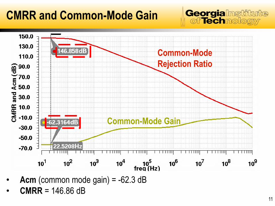
CMRR and Common-Mode Gain
• Acm (common mode gain) = -62.3 dB
• CMRR = 146.86 dB
Common-Mode
Rejection Ratio
Common-Mode Gain

12
Transient AC Response
• The resistive divider of 200k and 2M in non-inverting amplifier creates an AC gain
of 11, which is the expected ideal closed-loop gain of a non-inverting amplifier.
Vout
Vin
13
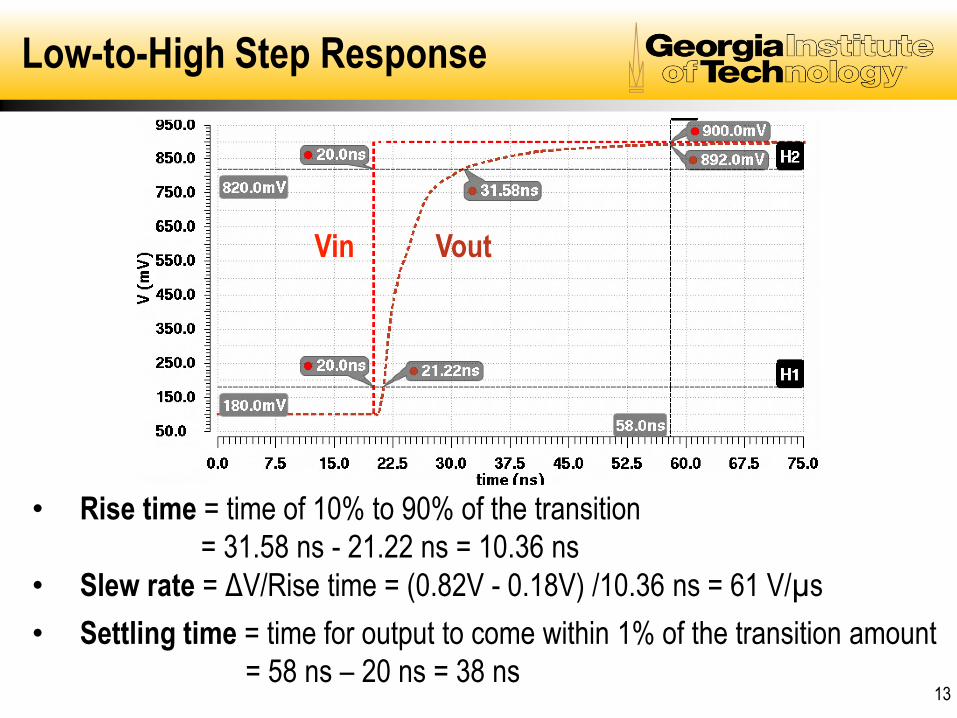
Low-to-High Step Response
• Rise time = time of 10% to 90% of the transition
= 31.58 ns - 21.22 ns = 10.36 ns
• Slew rate = ΔV/Rise time = (0.82V - 0.18V) /10.36 ns = 61 V/µs
• Settling time = time for output to come within 1% of the transition amount
= 58 ns – 20 ns = 38 ns
Vin Vout

14
High-to-Low Step Response
Vin Vout
• Fall time = time from 90% to 10% of the transition
= 125.3 ns – 121 ns = 4.3 ns
• Slew rate = ΔV/Fall time = (0.18 V - 0.82 V) / 4.3 ns = 148 V/µs
• Settling time = time for output to come within 1% of the transition amount
= 132.87 ns – 120 ns = 12.87 ns
15
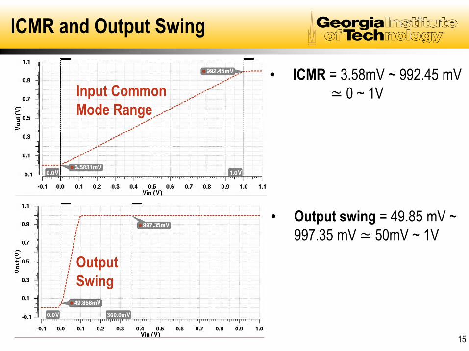
ICMR and Output Swing
• ICMR = 3.58mV ~ 992.45 mV
≃ 0 ~ 1V
• Output swing = 49.85 mV ~
997.35 mV ≃ 50mV ~ 1V
Input Common
Mode Range
Output
Swing
16
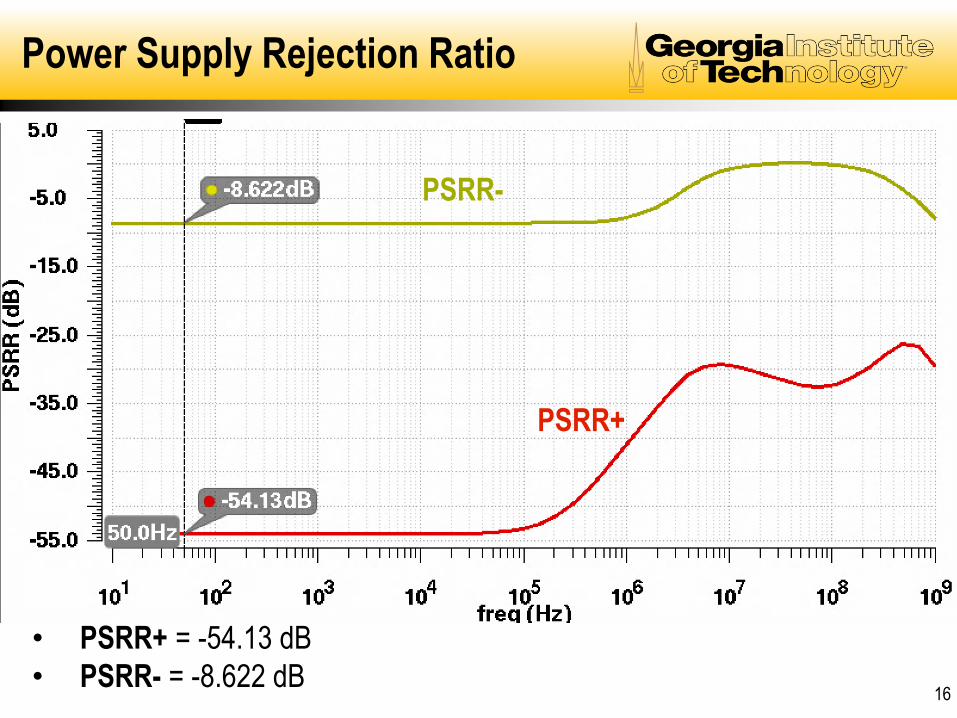
Power Supply Rejection Ratio
PSRR+
PSRR-
• PSRR+ = -54.13 dB
• PSRR- = -8.622 dB
17
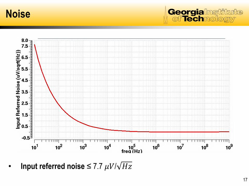
Noise
• Input referred noise ≤ 7.7 𝜇𝑉/ 𝐻𝑧
18
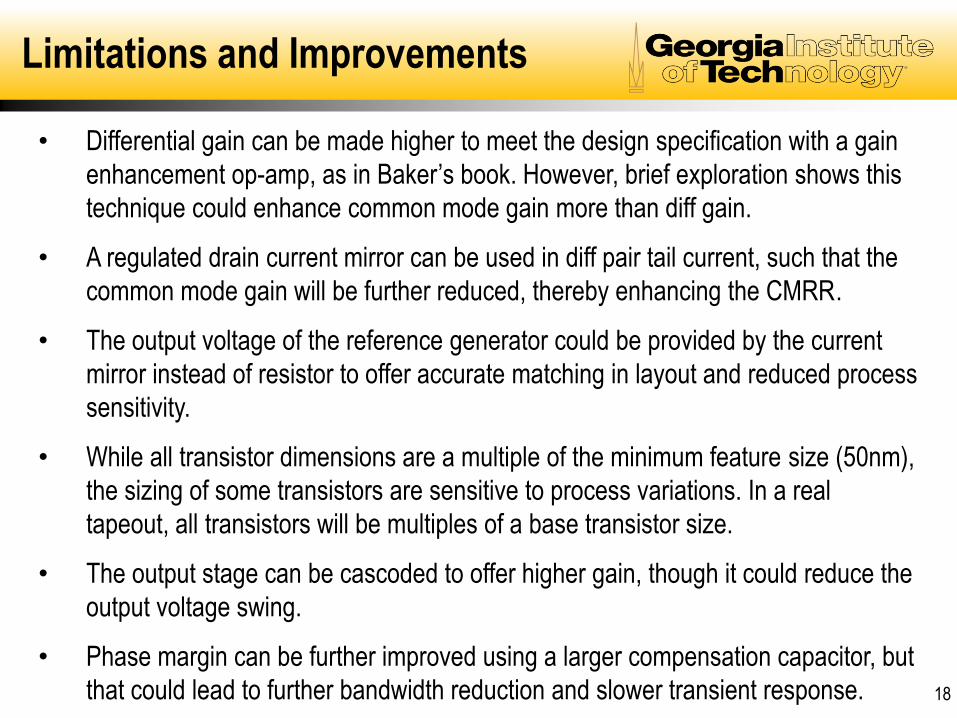
Limitations and Improvements
• Differential gain can be made higher to meet the design specification with a gain
enhancement op-amp, as in Baker’s book. However, brief exploration shows this
technique could enhance common mode gain more than diff gain.
• A regulated drain current mirror can be used in diff pair tail current, such that the
common mode gain will be further reduced, thereby enhancing the CMRR.
• The output voltage of the reference generator could be provided by the current
mirror instead of resistor to offer accurate matching in layout and reduced process
sensitivity.
• While all transistor dimensions are a multiple of the minimum feature size (50nm),
the sizing of some transistors are sensitive to process variations. In a real
tapeout, all transistors will be multiples of a base transistor size.
• The output stage can be cascoded to offer higher gain, though it could reduce the
output voltage swing.
• Phase margin can be further improved using a larger compensation capacitor, but
that could lead to further bandwidth reduction and slower transient response.
19
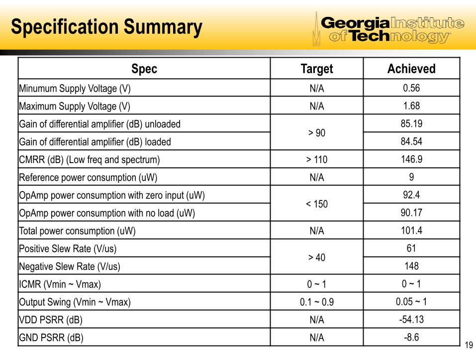
Specification Summary
Spec Target Achieved
Minumum Supply Voltage (V) N/A 0.56
Maximum Supply Voltage (V) N/A 1.68
Gain of differential amplifier (dB) unloaded> 90
85.19
Gain of differential amplifier (dB) loaded 84.54
CMRR (dB) (Low freq and spectrum) > 110 146.9
Reference power consumption (uW) N/A 9
OpAmp power consumption with zero input (uW)< 150
92.4
OpAmp power consumption with no load (uW) 90.17
Total power consumption (uW) N/A 101.4
Positive Slew Rate (V/us)> 40
61
Negative Slew Rate (V/us) 148
ICMR (Vmin ~ Vmax) 0 ~ 1 0 ~ 1
Output Swing (Vmin ~ Vmax) 0.1 ~ 0.9 0.05 ~ 1
VDD PSRR (dB) N/A -54.13
GND PSRR (dB) N/A -8.6
20
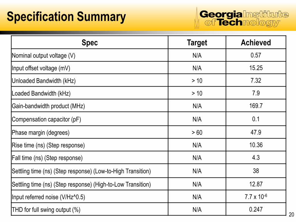
Specification Summary
Spec Target Achieved
Nominal output voltage (V) N/A 0.57
Input offset voltage (mV) N/A 15.25
Unloaded Bandwidth (kHz) > 10 7.32
Loaded Bandwidth (kHz) > 10 7.9
Gain-bandwidth product (MHz) N/A 169.7
Compensation capacitor (pF) N/A 0.1
Phase margin (degrees) > 60 47.9
Rise time (ns) (Step response) N/A 10.36
Fall time (ns) (Step response) N/A 4.3
Settling time (ns) (Step response) (Low-to-High Transition) N/A 38
Settling time (ns) (Step response) (High-to-Low Transition) N/A 12.87
Input referred noise (V/Hz^0.5) N/A 7.7 x 10⁻⁶
THD for full swing output (%) N/A 0.247
Recommended