EE141
1
EE141EE141--Spring 2008Spring 2008Digital Integrated Digital Integrated CircuitsCircuitsCircuitsCircuits
Lecture 5Lecture 5
EE141EECS141 1Lecture #5
MOS Transistor ModelMOS Transistor Model
AnnouncementsAnnouncementsDue to family emergency, Prof. Rabaey will be out of town this week and next.
We 2/6 : NO lecture – moved to 2/19Fr. 2/8:: Prof. AlonWe 2/13: NO lecture – moved to 2/26Fr 2/15: Simone GambiniTu 2/19: Make up lecture (203 McLaughlin)Tu 2/26: Make up lecture (203 McLaughlin)
EE141EECS141 2Lecture #5
p ( g )Lab 2 this week!
Lab 3 next weekHomework #2 is due Fr.

EE141
2
Class MaterialClass MaterialLast lecture
Design RulesStarted MOS modeling
Today’s lectureMOS transistor modeling
– Will see how to use these models to
EE141EECS141 3Lecture #5
understand tradeoffs between CMOS gate delay, power, etc.
Reading (3.3.1-3.3.2)
MOS TransistorMOS Transistor
Last lecture: what causes a transistor to turn on - concept
EE141EECS141 4Lecture #5
transistor to turn on concept of the threshold voltage
EE141
3
DSGVGS
+
–
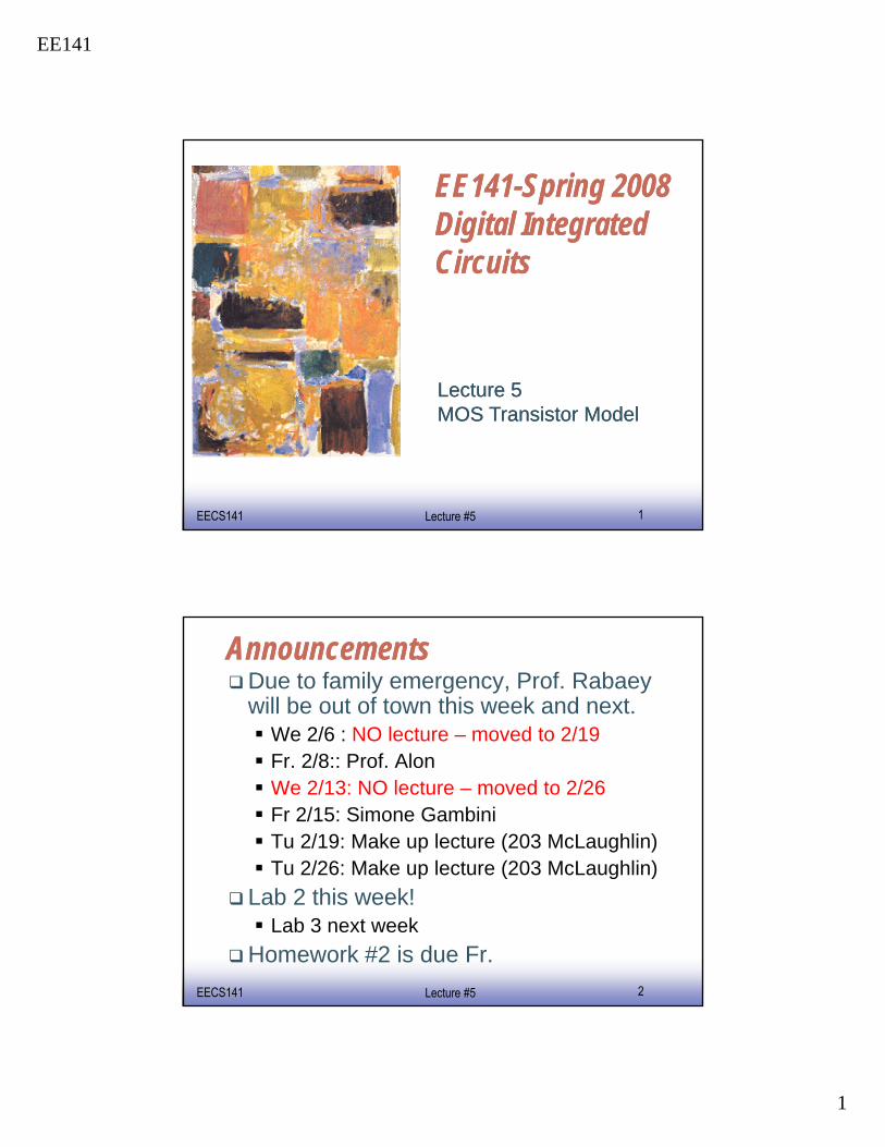
Threshold Voltage: ConceptThreshold Voltage: Concept
n+
p-substrate
B
Depletionregion
n-channel
n+
EE141EECS141 5Lecture #5
BWith positive gate bias, electrons pulled toward the gateWith large enough bias, enough electrons will be pulled to "invert" the surface (p→n type)Voltage at which surface inverts: “magic” threshold voltage VT
The Threshold VoltageThe Threshold VoltageThreshold
Depletion charge2 BT FB F
QVC
ϕ ϕ= + +
iA
TF nNln⋅φ=φ
Fermi potential( )0 2 2T T F SB FV V Vγ ϕ ϕ= + ⋅ + −
oxC
EE141EECS141 6Lecture #5
2ΦF is approximately 0.6V for p-type substratesγ is the body factorVT0 is approximately 0.45V for our process

EE141
4
SVGS VDS
Transistor with Gate and Drain BiasTransistor with Gate and Drain Bias
n+n+
D
SG
xL
V(x) +–
ID
EE141EECS141 7Lecture #5
p-substrate
B
The Drain CurrentThe Drain Current
( )iQ x =
Charge density:
i
Velocity:
( )n xυ =
Current:
EE141EECS141 8Lecture #5
DI =
Current:
EE141
5
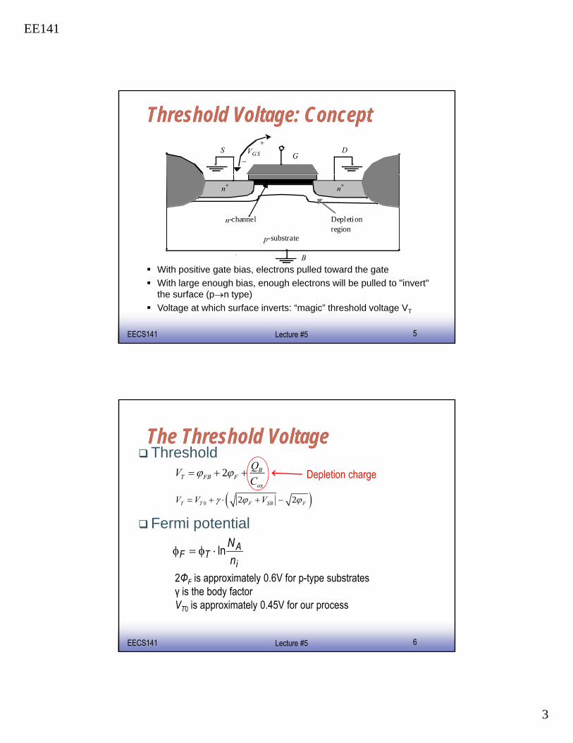
Solving the Drain CurrentSolving the Drain CurrentIntegrate along the channel:
EE141EECS141 9Lecture #5
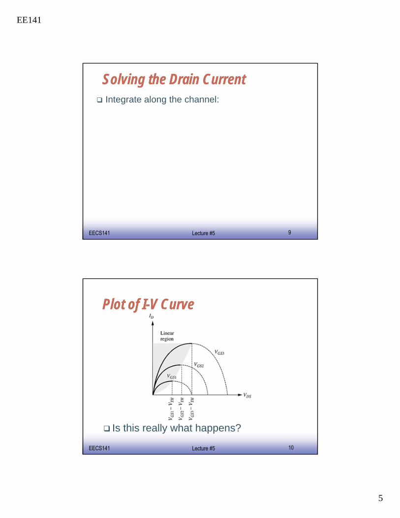
Plot of IPlot of I--V CurveV Curve
EE141EECS141 10Lecture #5
Is this really what happens?
EE141
6
VGS
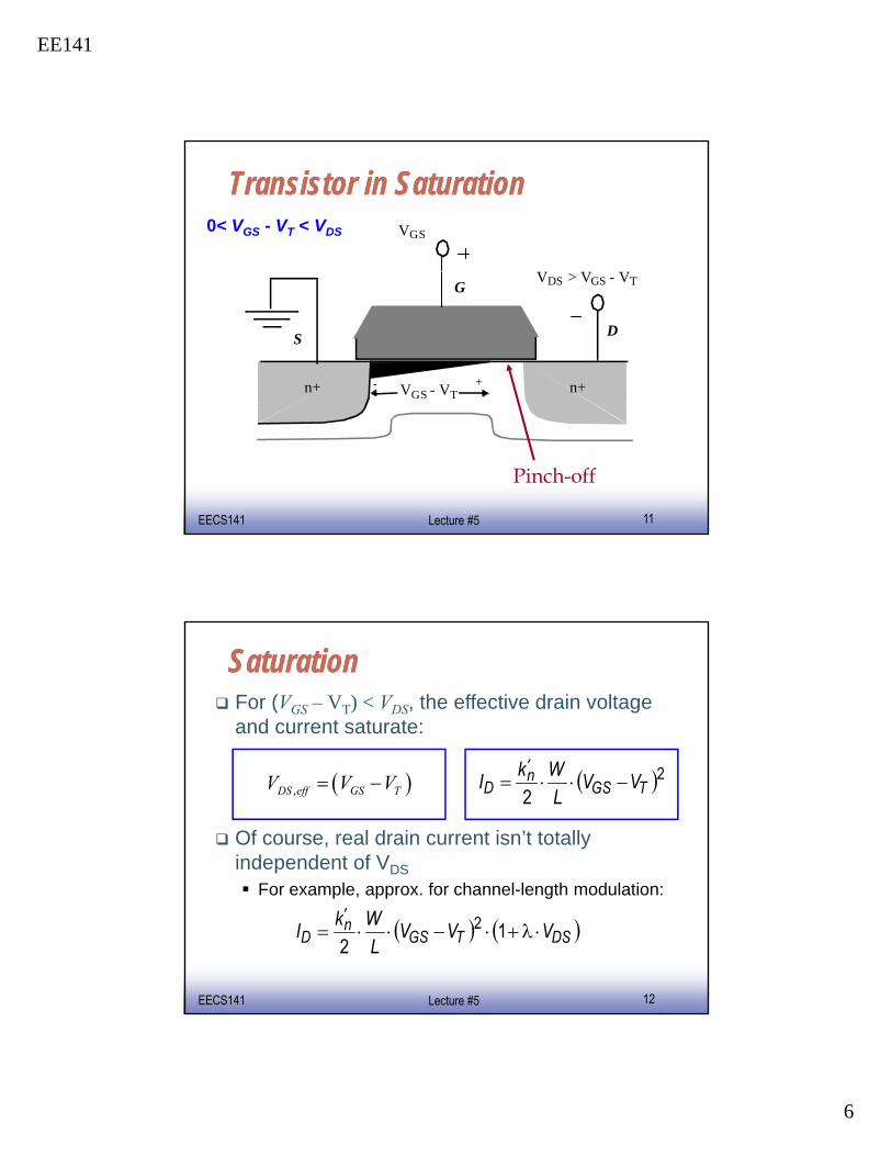
Transistor in SaturationTransistor in Saturation0< VGS - VT < VDS
n+n+
S
G
D
VDS > VGS - VT
VGS - VT+-
EE141EECS141 11Lecture #5
Pinch-off
SaturationSaturationFor (VGS – VT) < VDS, the effective drain voltage and current saturate:
( )22 TGSn
D VVL
WkI −⋅⋅=’
Of course, real drain current isn’t totally independent of VDS
F l f h l l th d l ti
( ),DS eff GS TV V V= −
EE141EECS141 12Lecture #5
For example, approx. for channel-length modulation:
( ) ( )DSTGSn
D VVVL
WkI ⋅λ+⋅−⋅⋅= 12
2’
EE141
7
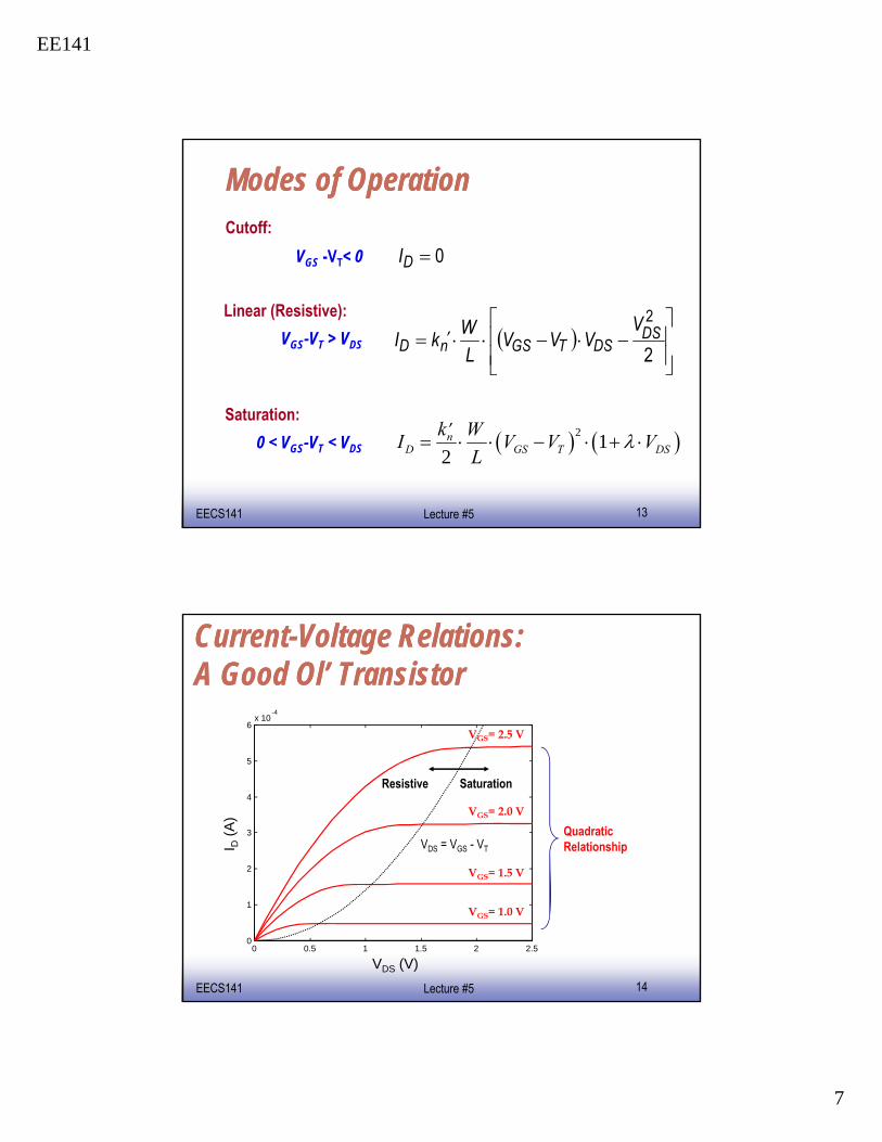
Modes of OperationModes of OperationCutoff:
VGS -VT< 0 0=DI
Linear (Resistive):VGS-VT > VDS ( )
⎥⎥⎦
⎤
⎢⎢⎣
⎡−⋅−⋅⋅=
2
2DS
DSTGSnDV
VVVL
WkI ’
EE141EECS141 13Lecture #5
Saturation:0 < VGS-VT < VDS ( ) ( )2 1
2n
D GS T DSk WI V V V
Lλ= ⋅ ⋅ − ⋅ + ⋅
’
6x 10
-4
VGS= 2.5 V
CurrentCurrent--Voltage Relations:Voltage Relations:A Good Ol’ TransistorA Good Ol’ Transistor
QuadraticRelationship
2
3
4
5
VGS= 2.0 V
V = 1 5 V
Resistive Saturation
VDS = VGS - VTI D(A
)
EE141EECS141 14Lecture #5
0 0.5 1 1.5 2 2.50
1
VGS= 1.5 V
VGS= 1.0 V
VDS (V)
EE141
8
-4
2.5x 10
V = 2 5 VEarly
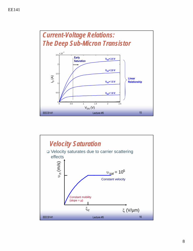
CurrentCurrent--Voltage Relations:Voltage Relations:The Deep SubThe Deep Sub--Micron TransistorMicron Transistor
LinearRelationship1
1.5
2
VGS= 2.5 V
VGS= 2.0 V
VGS= 1.5 V
ySaturation
I D(A
)
EE141EECS141 15Lecture #5
0 0.5 1 1.5 2 2.50
0.5 VGS= 1.0 V
VDS (V)
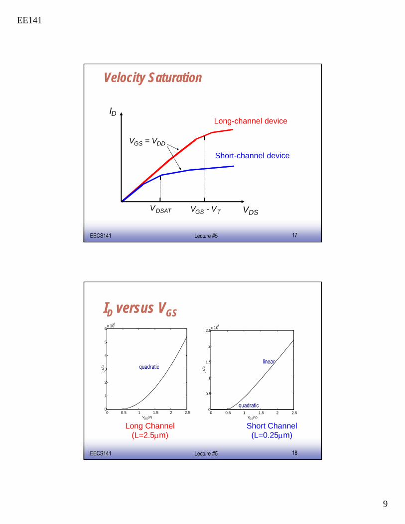
Velocity SaturationVelocity Saturation
s)
Velocity saturates due to carrier scattering effects
υn
(m/s
υsat = 105
Constant velocity
EE141EECS141 16Lecture #5
ξ (V/µm)
Constant mobility (slope = µ)
ξc
EE141
9
Velocity SaturationVelocity Saturation
IDLong-channel deviceLong channel device
Short-channel device
VGS = VDD
EE141EECS141 17Lecture #5
VDSVDSAT VGS - VT
IIDD versus Vversus VGSGS
5
6x 10⁻⁴
2.5x 10⁻⁴
1
2
3
4
5
I D(A
)
0.5
1
1.5
2
I D(A
)quadraticlinear
EE141EECS141 18Lecture #5
0 0.5 1 1.5 2 2.50
VGS(V)0 0.5 1 1.5 2 2.5
0
VGS(V)
quadratic
Long Channel(L=2.5μm)
Short Channel(L=0.25μm)
EE141
10
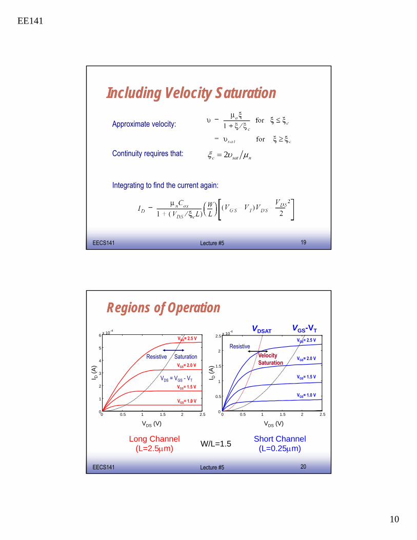
Including Velocity SaturationIncluding Velocity Saturation
Approximate velocity:pp y
Continuity requires that:
Integrating to find the current again:
2c sat nξ υ μ=
EE141EECS141 19Lecture #5
g g g
Regions of OperationRegions of Operation-4
2
2.5 x 10VGS= 2.5 V
5
6 x 10⁻⁴
VGS= 2.5 VResistive
VDSAT VGS-VT
0
0.5
1
1.5
2
VGS= 2.0 V
VGS= 1.5 V
VGS= 1.0 V
0
1
2
3
4VGS= 2.0 V
VGS= 1.5 V
VGS= 1.0 V
Resistive Saturation
VDS = VGS - VTI D(A
)
I D(A
)
VelocitySaturation
EE141EECS141 20Lecture #5
0 0.5 1 1.5 2 2.500 0.5 1 1.5 2 2.50
VDS (V) VDS (V)
Long Channel(L=2.5μm)
Short Channel(L=0.25μm)W/L=1.5

EE141
11
Simplified Velocity SaturationSimplified Velocity Saturation
s)
Assume velocity linear until hit υsat
υn
(m/s
υsat = 105
Constant velocity
EE141EECS141 21Lecture #5
ξ (V/µm)ξc= υsat/μ
Simplified Velocity Saturation Simplified Velocity Saturation (cont’d)(cont’d)
Assume VDSAT = ξcL when (VGS – VT) > ξcL
V)V
DS
AT(V
ξcL
Actual VDSAT
EE141EECS141 22Lecture #5
VGS-VT (V)ξcL

EE141
12
Simplified ModelSimplified Model
-4
2.5x 10
V V
Define VGT = VGS – VT, VVSAT = ξc·L
1
1.5
2 VelocitySaturation
I D(A
)
Linear
VDS = VVSAT
EE141EECS141 23Lecture #5
0 0.5 1 1.5 2 2.50
0.5
VDS (V)
VDS = VGT
VGT = VVSAT
Saturation
A Unified Model for Manual AnalysisA Unified Model for Manual Analysis
define VGT = VGS – VT
D
G
ID
S
( )2
,' 1DS effVWI k V V Vλ⎛ ⎞
+⎜ ⎟
for VGT ≤ 0: ID = 0
for VGT ≥ 0:
GT GS T
EE141EECS141 24Lecture #5
B( ),
,' 12
ffD GT DS eff DSI k V V V
Lλ= ⋅ ⋅ ⋅ − ⋅ + ⋅⎜ ⎟⎜ ⎟
⎝ ⎠
with VDS,eff = min (VGT, VDS, VVSAT)
EE141
13
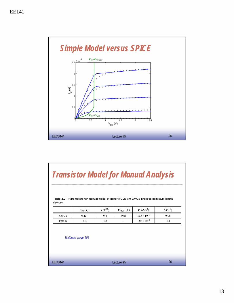
Simple Model versus SPICE Simple Model versus SPICE 2.5
x 10-4 VDS=VVSAT
1
1.5
2
I D(A
)
EE141EECS141 25Lecture #5
0 0.5 1 1.5 2 2.50
0.5
VDS (V)
VDS=VGT
Transistor Model for Manual AnalysisTransistor Model for Manual Analysis
V
EE141EECS141 26Lecture #5
Textbook: page 103
EE141
14
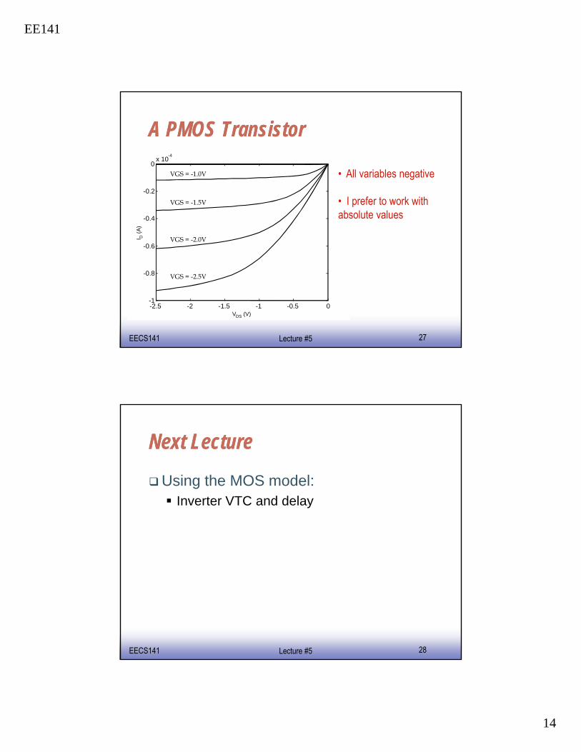
A PMOS TransistorA PMOS Transistor0
x 10-4
• All variables negativeVGS = -1.0V
-0.6
-0.4
-0.2
I D(A
)
All variables negative
• I prefer to work with absolute values
VGS = -1.5V
VGS = -2.0V
EE141EECS141 27Lecture #5
-2.5 -2 -1.5 -1 -0.5 0-1
-0.8
VDS (V)
VGS = -2.5V
Next LectureNext LectureUsing the MOS model:
Inverter VTC and delay
EE141EECS141 28Lecture #5
Recommended