EECS425 – Winter 2016 Group B
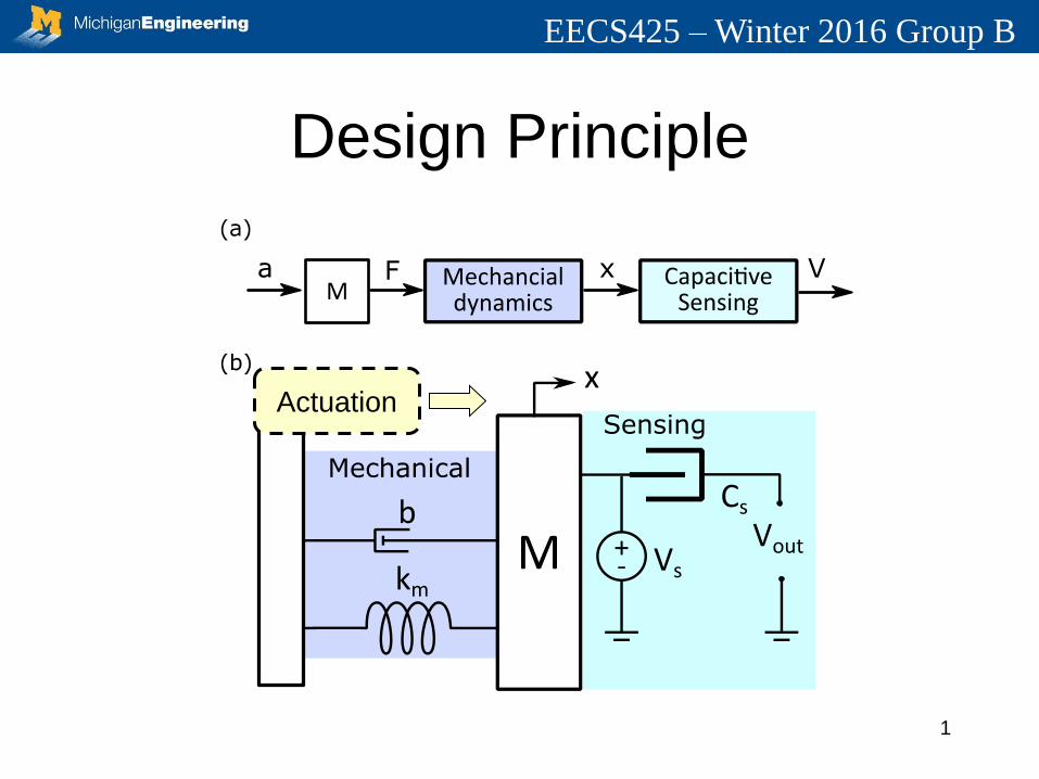
Design Principle
1
Actuation
EECS425 – Winter 2016 Group B
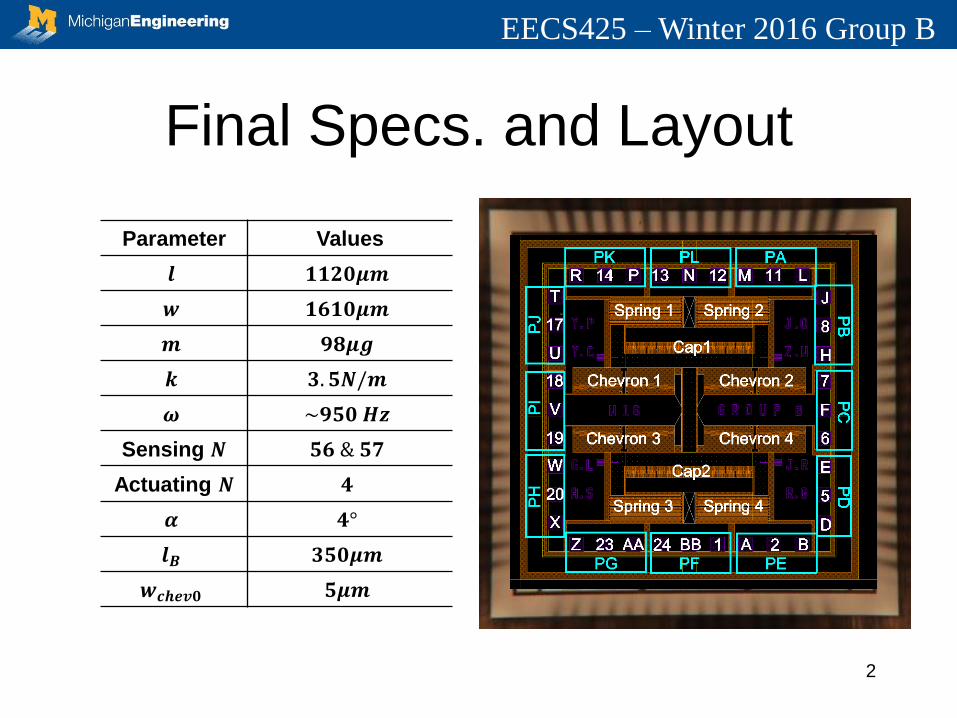
Final Specs. and Layout
2
Parameter Values
𝒍 𝟏𝟏𝟐𝟎𝝁𝒎
𝒘 𝟏𝟔𝟏𝟎𝝁𝒎
𝒎 𝟗𝟖𝝁𝒈
𝒌 𝟑. 𝟓𝑵/𝒎
𝝎 ~𝟗𝟓𝟎 𝑯𝒛
Sensing 𝑵 𝟓𝟔 & 𝟓𝟕
Actuating 𝑵 𝟒
𝜶 𝟒°
𝒍𝑩 𝟑𝟓𝟎𝝁𝒎
𝒘𝒄𝒉𝒆𝒗𝟎 𝟓𝝁𝒎
EECS425 – Winter 2016 Group B
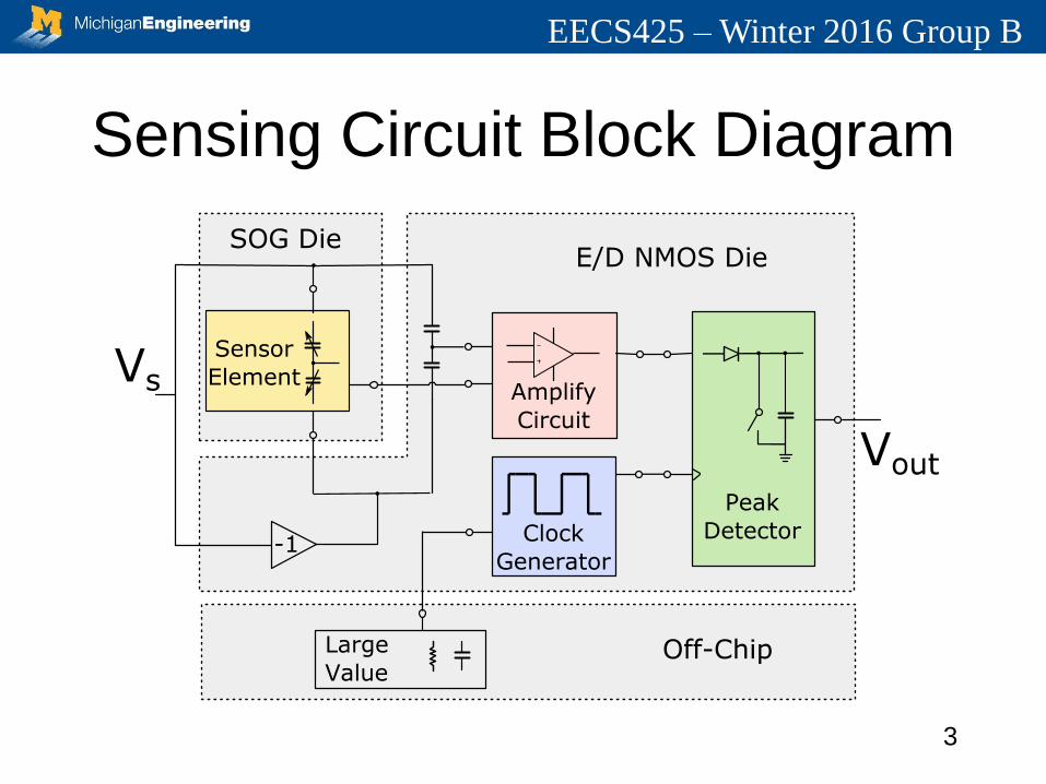
Sensing Circuit Block Diagram
3
EECS425 – Winter 2016 Group B
4
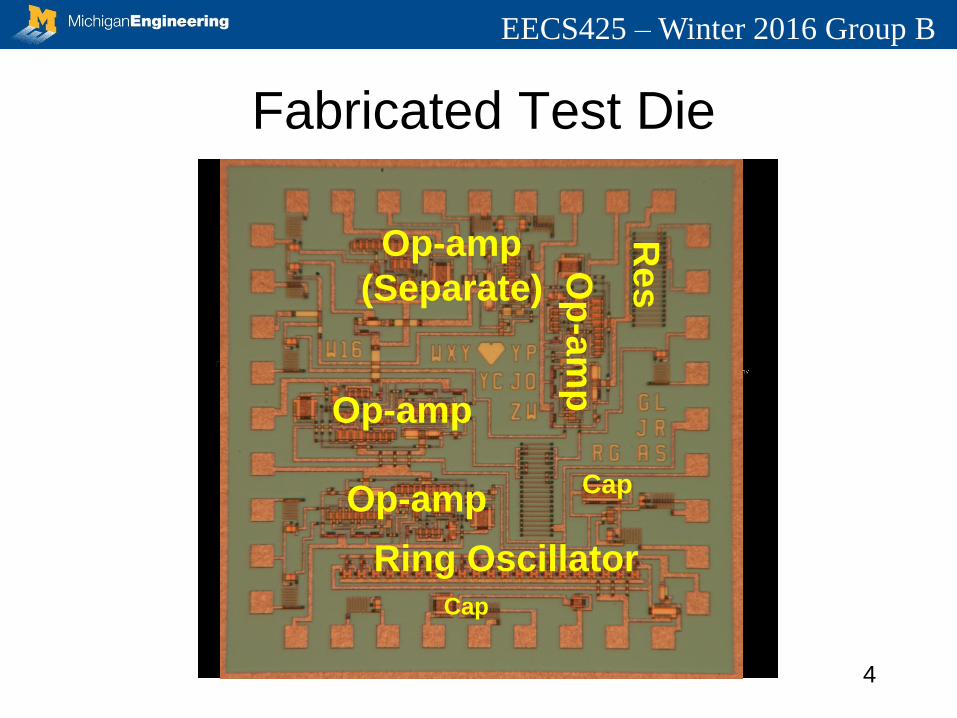
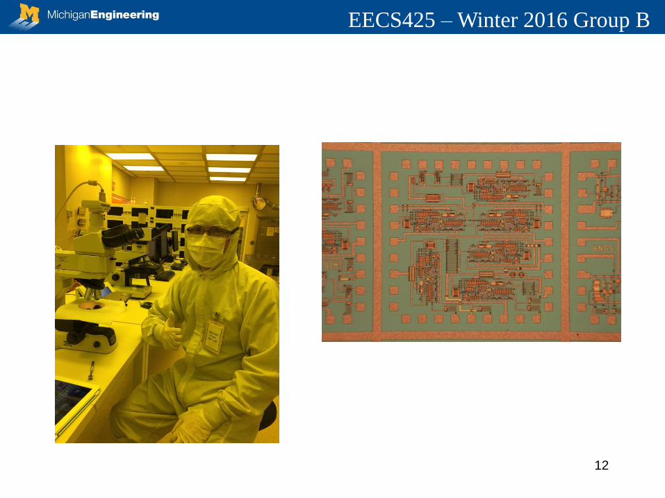
Fabricated Test Die
Ring Oscillator
Op-amp
Op-amp
Op
-am
p
Res
Cap
Op-amp
(Separate)
Cap
EECS425 – Winter 2016 Group B
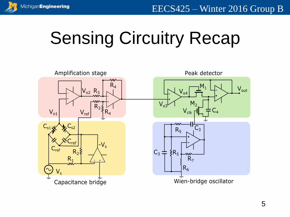
Sensing Circuitry Recap
5
06/04/2014
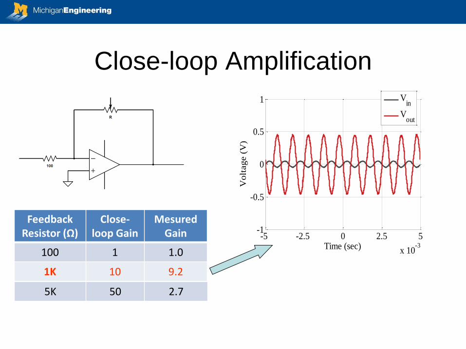
Close-loop Amplification
Feedback Resistor (Ω)
Close-loop Gain
Mesured Gain
100 1 1.0
1K 10 9.2
-5 -2.5 0 2.5 5
x 10-3
-1
-0.5
0
0.5
1
Time (sec)V
olt
ag
e (
V)
Vin
Vout
5K 50 2.7
EECS425 – Winter 2016 Group B
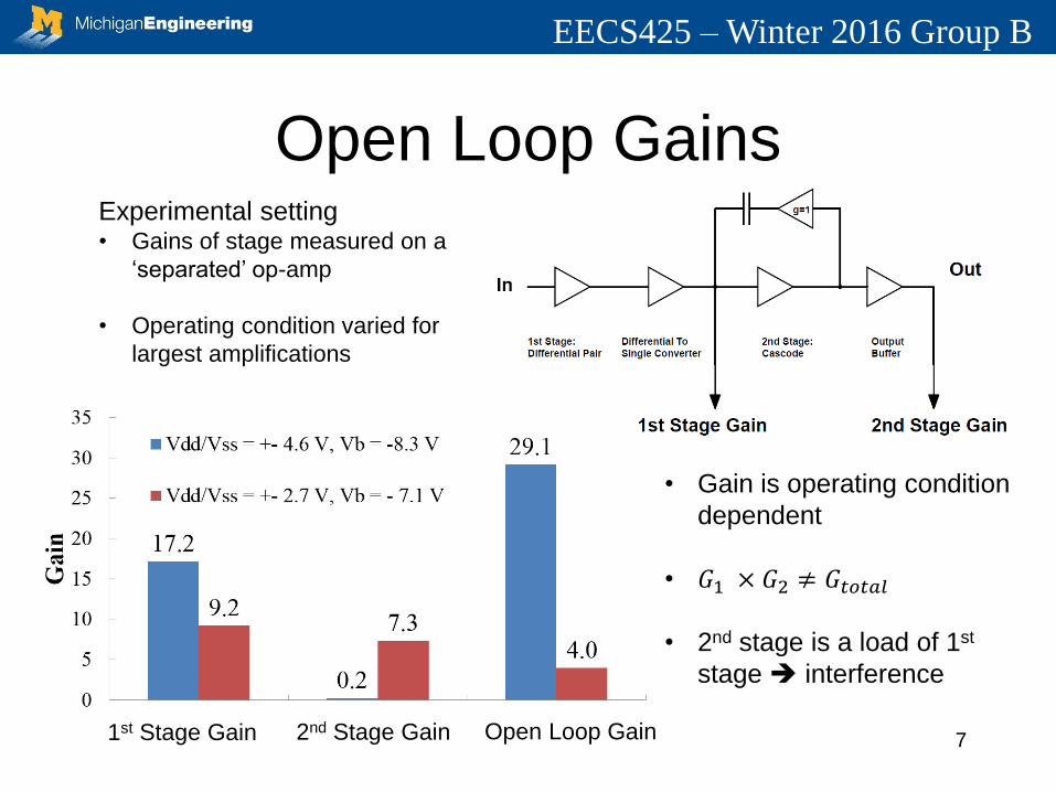
Open Loop Gains
7
• Gain is operating condition
dependent
• 𝐺1 × 𝐺2 ≠ 𝐺𝑡𝑜𝑡𝑎𝑙
• 2nd stage is a load of 1st
stage interference
Experimental setting • Gains of stage measured on a
‘separated’ op-amp
• Operating condition varied for
largest amplifications
1st Stage Gain 2nd Stage Gain Open Loop Gain
06/04/2014
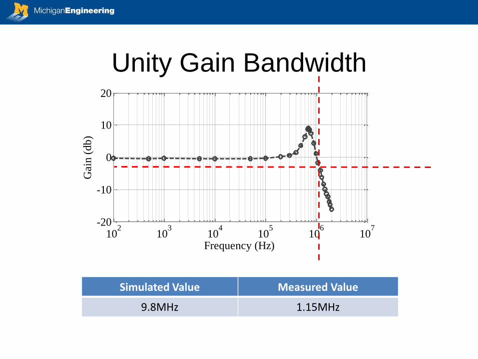
Unity Gain Bandwidth
102
103
104
105
106
107
-20
-10
0
10
20
Frequency (Hz)
Gain
(d
b)
102
103
104
105
106
107
-300
-200
-100
0
100
Frequency (Hz)
Ph
ase
(d
eg
)
Simulated Value Measured Value
9.8MHz 1.15MHz
06/04/2014
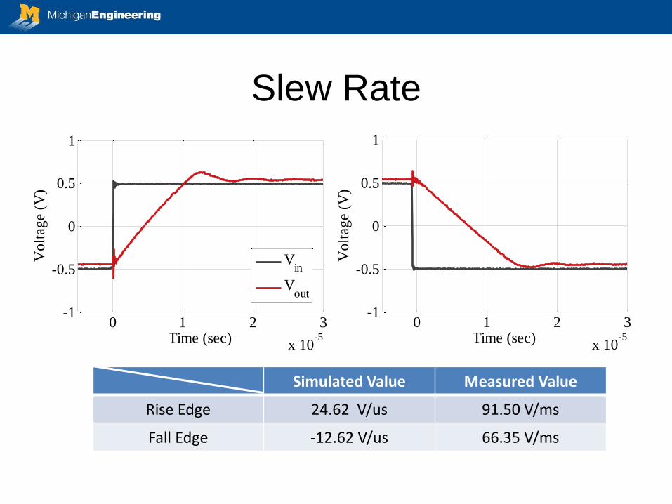
Slew Rate
0 1 2 3
x 10-5
-1
-0.5
0
0.5
1
Time (sec)
Vo
ltag
e (
V)
Vin
Vout
0 1 2 3
x 10-5
-1
-0.5
0
0.5
1
Time (sec)
Vo
ltag
e (
V)
0 1 2 3
x 10-5
-1
-0.5
0
0.5
1
Time (sec)
Volt
age (
V)
Vin
Vout
0 1 2 3
x 10-5
-1
-0.5
0
0.5
1
Time (sec)V
olt
age (
V)
Simulated Value Measured Value
Rise Edge 24.62 V/us 91.50 V/ms
Fall Edge -12.62 V/us 66.35 V/ms
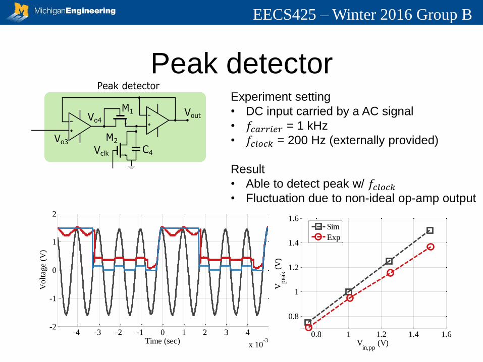
EECS425 – Winter 2016 Group B
Peak detector
10 -4 -3 -2 -1 0 1 2 3 4
x 10-3
-2
-1
0
1
2
Time (sec)
Volt
age (
V)
Vin
Vpeak,exp
Vpeak,sim
Experiment setting
• DC input carried by a AC signal
• 𝑓𝑐𝑎𝑟𝑟𝑖𝑒𝑟 = 1 kHz
• 𝑓𝑐𝑙𝑜𝑐𝑘 = 200 Hz (externally provided)
Result
• Able to detect peak w/ 𝑓𝑐𝑙𝑜𝑐𝑘
• Fluctuation due to non-ideal op-amp output
0.8 1 1.2 1.4 1.6
0.8
1
1.2
1.4
1.6
Vin,pp
(V)
Vp
eak (
V)
Sim
Exp
EECS425 – Winter 2016 Group B
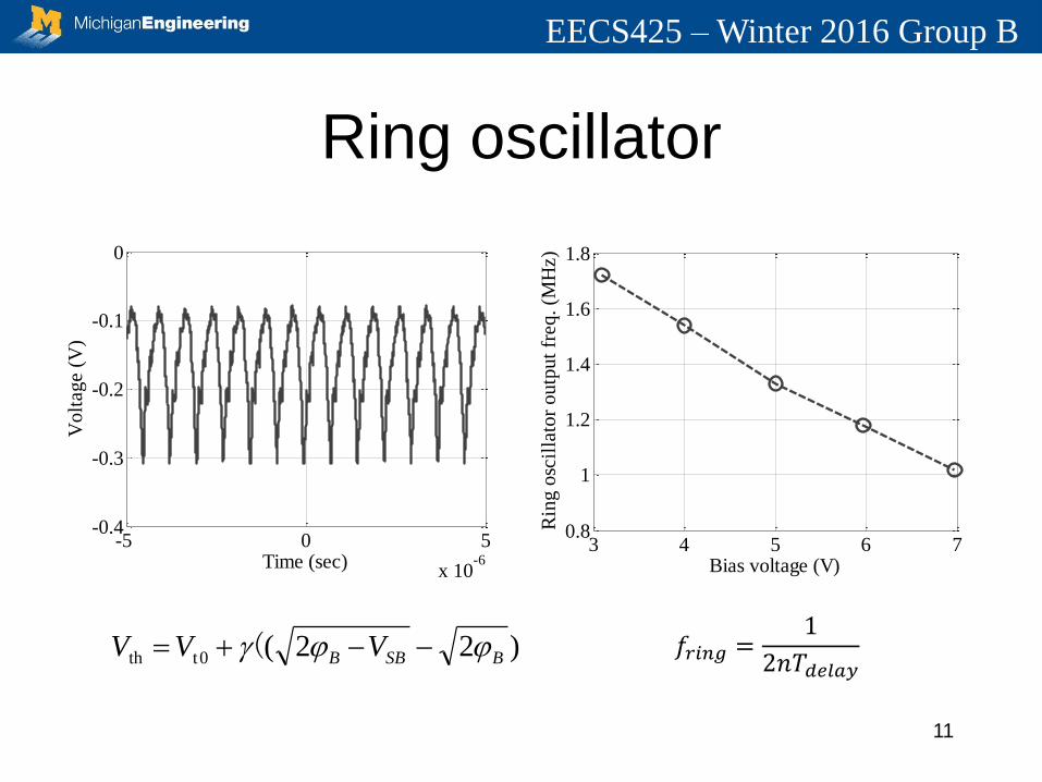
Ring oscillator
11
3 4 5 6 70.8
1
1.2
1.4
1.6
1.8
Bias voltage (V)R
ing
osc
illa
tor
ou
tpu
t fr
eq
. (M
Hz)
-5 0 5
x 10-6
-0.4
-0.3
-0.2
-0.1
0
Time (sec)
Volt
age (
V)
𝑓𝑟𝑖𝑛𝑔 =1
2𝑛𝑇𝑑𝑒𝑙𝑎𝑦 )22((0tth BSBB VVV
EECS425 – Winter 2016 Group B
12
EECS425 – Winter 2016 Group B
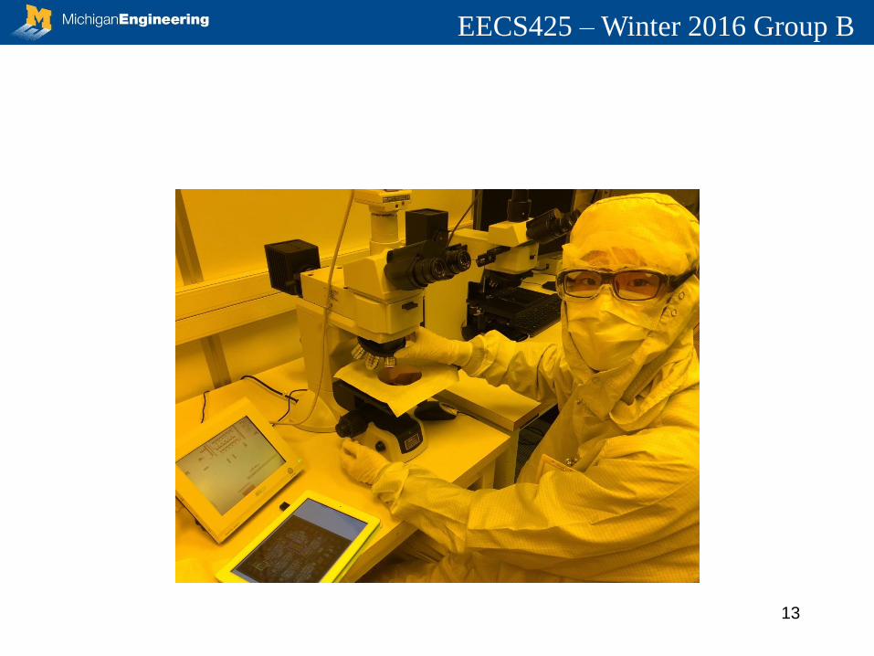
13
Recommended