BeagleBone Black
AM335X
Burden +
Protection
Protection
LDOLP2992
LDOTPS7A39
LDOTPS7A6533
DC/DC ConverterTPS65131
Load Switch
TPS22914
LED
LED
TIDA-01555
V1
V2
V3
I1
I2
I3
8 I/Ps
CT
CT
CT
CT
PT
PT
PT
PTV4
I4
SCLK6x
Voltage Supply
AVDD: 5 V
DVDD: 3.3 V
+14 V
-14 V
+12 V
-12 V
AVcc+5.5 V
Analog Signal Conditioning Interface Adaptor Card
Sitara EVM
Power Tree
Sensor Board-1
Sensor Board-6
ADCADS8688
OPA4197
OPA4197
Clock BufferCDCLVC1106
ADCADS8688
Con
nect
or
Con
nect
or
Con
nect
or
Con
nect
or
Con
nect
orC
onne
ctor
Pro
tect
ion
Copyright © 2017, Texas Instruments Incorporated
1TIDUDN4–December 2017Submit Documentation Feedback
Copyright © 2017, Texas Instruments Incorporated
Flexible Interface (PRU-ICSS) Reference Design for Simultaneous, CoherentDAQ Using Multiple ADCs
TI Designs: TIDA-01555Flexible Interface (PRU-ICSS) Reference Design forSimultaneous, Coherent DAQ Using Multiple ADCs
DescriptionThis reference design showcases an interfaceimplementation for connecting six high-voltage bipolarinput, 8-channel, mux-input SAR ADCs with theSitara™ Arm® processors for expanding the number ofinput channels using programmable real-time units(PRU-ICSS). ADCs are configured to sample the samechannels simultaneously across all ADCs. The designhighlights the capability of PRU-ICSS to handle a1536-ksps (each sample = 16 bits) data rate bysampling 640 samples per line cycle. For a 50-Hzcycle, this corresponds to 32 ksps per channel acrosssix ADCs simultaneously (640 samples/cycle × 50 Hz× 6 ADCs × 8 Channels = 1536 ksps). Also, thesecond PRU is used to post process the data toachieve coherent sampling.
Resources
TIDA-01555 Design FolderADS8688 Product FolderBEAGLEBK Tool FolderOPA4197 Product FolderTPS22914 Product FolderTPS65131 Product FolderTPS7A6533 Product FolderTPS7A39 Product FolderLP2992 Product FolderCDCLVC1106 Product Folder
ASK Our E2E™ Experts
Features• Flexible Interface Using PRU-ICSS (Sitara
Processor) to Communicate With MultipleSAR ADCs
• AC Voltage and Current Measurement Accuracy:– AC Voltage: < ±0.2% for 2.5 V to 120 V– AC Current: < ±0.2% for 2.5 A to 70 A– Simultaneous Sampling Across Six ADCs
(16-bit, 500 ksps/ADC)• PRU-ICSS Interface:
– PRU-ICSS Offers Flexible Data Capture forChannel Expansion
– Firmware-Based Approach Allows for ReuseAcross Different Sitara Processors
– Coherent Sampling Achieved by ComputingLine Cycle in Software and by AdjustingCS Signal
Applications• Protection Relay, IEDs• Terminal Units• Merging Units• Programmable Logic Control (PLC)• Avionics• Instrumentation
System Description www.ti.com
2 TIDUDN4–December 2017Submit Documentation Feedback
Copyright © 2017, Texas Instruments Incorporated
Flexible Interface (PRU-ICSS) Reference Design for Simultaneous, CoherentDAQ Using Multiple ADCs
An IMPORTANT NOTICE at the end of this TI reference design addresses authorized use, intellectual property matters and otherimportant disclaimers and information.
1 System DescriptionIn sectors such as grid infrastructure, factory automation, test and measurements , and so on, there arevarious applications in which multiple analog signals from sensors need to be captured on a singleprocessor for monitoring and protection of critical equipment. In these scenarios, multiple analog-to-digitalconverters (ADCs) convert the analog signals from transducers to digital domain for further processing orto communicate through the network. Choosing a converter with good performance with very highresolution and parametric data is only one half of the equation. When more than two ADCs need to beinterfaced with a single processor, choosing the right processor becomes challenging due to limitedperipherals. The choice becomes narrower if more ADCs need to be interfaced with higher throughput.Controlling the timing of the interface and control signals along with the jitter is equally as important as ithelps in accurate data representation with minimal spectral leakages.
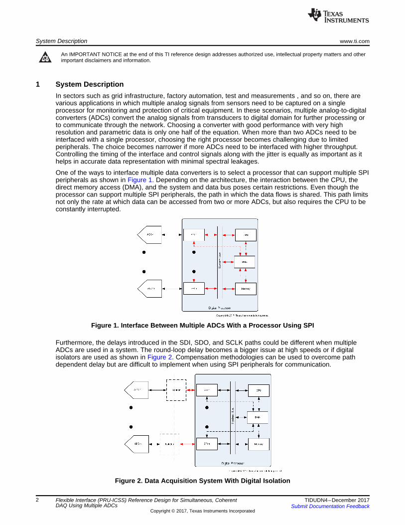
One of the ways to interface multiple data converters is to select a processor that can support multiple SPIperipherals as shown in Figure 1. Depending on the architecture, the interaction between the CPU, thedirect memory access (DMA), and the system and data bus poses certain restrictions. Even though theprocessor can support multiple SPI peripherals, the path in which the data flows is shared. This path limitsnot only the rate at which data can be accessed from two or more ADCs, but also requires the CPU to beconstantly interrupted.
Figure 1. Interface Between Multiple ADCs With a Processor Using SPI
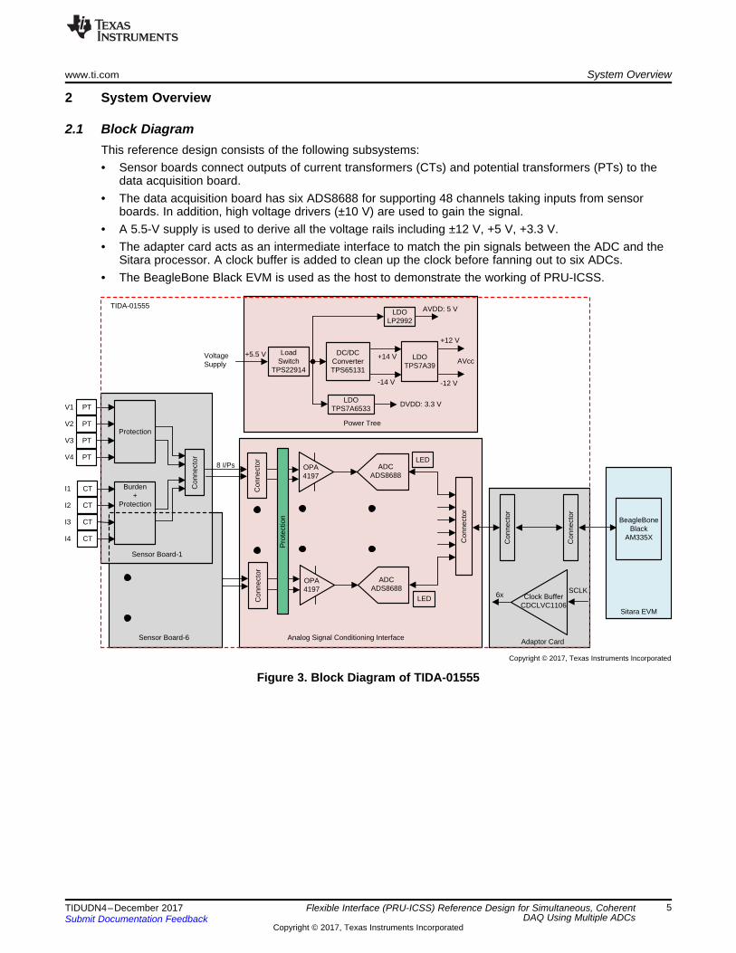
Furthermore, the delays introduced in the SDI, SDO, and SCLK paths could be different when multipleADCs are used in a system. The round-loop delay becomes a bigger issue at high speeds or if digitalisolators are used as shown in Figure 2. Compensation methodologies can be used to overcome pathdependent delay but are difficult to implement when using SPI peripherals for communication.
Figure 2. Data Acquisition System With Digital Isolation

www.ti.com System Description
3TIDUDN4–December 2017Submit Documentation Feedback
Copyright © 2017, Texas Instruments Incorporated
Flexible Interface (PRU-ICSS) Reference Design for Simultaneous, CoherentDAQ Using Multiple ADCs
FPGAs are used as an intermediate interface element to overcome these issues. This reference designshowcases how to implement a flexible interface that can simultaneously connect with six ADCs using theSitara processor. The PRU-ICSS subsystem integrated in the processor are used for both data acquisitionand for data computation. This frees up the bandwidth of the Arm core as the interface and processingcan now be handled independent of the core CPU.
This reference design:• Provides data acquisition from 48 analog input channels using six ADCs• Does the analog signal conditioning for improved signal chain performance• Uses PRU-ICSS to adjust the time base for the communication interface to achieve coherent sampling
thereby reducing the spectral leakages
1.1 Protection RelayProtection Relays are used to improve the reliability and efficiency of the power systems in various stages.These stages include power generation to transmission and distribution by detecting defectivetransmission lines, apparatus or other abnormal power system conditions. These relays are placed tomonitor electrical parameters in the power systems or in the vicinity of primary equipment to detect anyabnormal conditions to prevent any damages. Protection relay consists of an AC analog input module,which acquires data from voltage and current sensors from different phases. In digital protection relays,data acquisition system consists of measurement of voltages and currents along with analog signalconditioning, data converters, and host interface to capture digital values providing post processing of theacquired data. In this application, flexible data acquisition shown in this reference design can be used toachieve required AC and DC performance.
1.2 Grid AutomationIn substation automation, terminal units and merging units collect and forward sensor data to intelligentelectronic devices (IEDs). These units collect the data from conventional or non-conventional instrumenttransformers and send the sampled current and voltage signals over the network. This reference designcan be used to interface and process the data using a single processor for very high speeds.
1.3 Other ApplicationsIn programmable logic controllers (PLCs) and other instrumentation systems in avionics and test andmeasurement, this reference design can be customized for different number of input channels to realizehigh-speed data acquisition system for simultaneous sampling.

System Description www.ti.com
4 TIDUDN4–December 2017Submit Documentation Feedback
Copyright © 2017, Texas Instruments Incorporated
Flexible Interface (PRU-ICSS) Reference Design for Simultaneous, CoherentDAQ Using Multiple ADCs
1.4 Key System Specifications
Table 1. Key System Specifications
PARAMETER SPECIFICATIONS DETAILS
ADC 16-bit, 8-channel, 500 ksps ADS8688 500-ksps, 8-Channel, 16-Bit, SARADC with Bipolar Input Ranges Section 2.2.1
Number of channels 48 channelsInput voltage range at transducer 120-V AC RMS Section 2.3.2Input current range at transducer 70-A AC RMS Section 2.3.2Input voltage range at ADC ±10.24 V ±20-V overvoltage protectionAC voltage accuracy < ±0.2% 2.5 to 120 V RMSAC current accuracy < ±0.2% 2.5 to 70 A RMS
Interface4-wire SPI (ADC)PRU-ICSS (processor)
SPI clock frequency10 MHz (for six ADCs)
Section 2.3.1.217 MHz (ADC max)25 MHz (PRU-ICSS max)
DC performanceCode spread of ≤ 4
Section 3.2.2.2Sigma ≤ 0.58
AC performance SFDR = 110 dB Fin = 64 Hz, number of points = 65536
Sampling frequency per input channel 32 ksps per channel across sixADCs Total throughput of 1536 ksps
Coherent sampling CS adjustment for input frequency50 Hz ± 10% Section 2.3.1.3.1
Power supply
5-V analog supply for ADS86883.3-V digital supply±12-V analog signal conditioning ofinput signals
BeagleBone Black
AM335X
Burden +
Protection
Protection
LDOLP2992
LDOTPS7A39
LDOTPS7A6533
DC/DC ConverterTPS65131
Load Switch
TPS22914
LED
LED
TIDA-01555
V1
V2
V3
I1
I2
I3
8 I/Ps
CT
CT
CT
CT
PT
PT
PT
PTV4
I4
SCLK6x
Voltage Supply
AVDD: 5 V
DVDD: 3.3 V
+14 V
-14 V
+12 V
-12 V
AVcc+5.5 V
Analog Signal Conditioning Interface Adaptor Card
Sitara EVM
Power Tree
Sensor Board-1
Sensor Board-6
ADCADS8688
OPA4197
OPA4197
Clock BufferCDCLVC1106
ADCADS8688
Con
nect
or
Con
nect
or
Con
nect
or
Con
nect
or
Con
nect
orC
onne
ctor
Pro
tect
ion
Copyright © 2017, Texas Instruments Incorporated
www.ti.com System Overview
5TIDUDN4–December 2017Submit Documentation Feedback
Copyright © 2017, Texas Instruments Incorporated
Flexible Interface (PRU-ICSS) Reference Design for Simultaneous, CoherentDAQ Using Multiple ADCs
2 System Overview
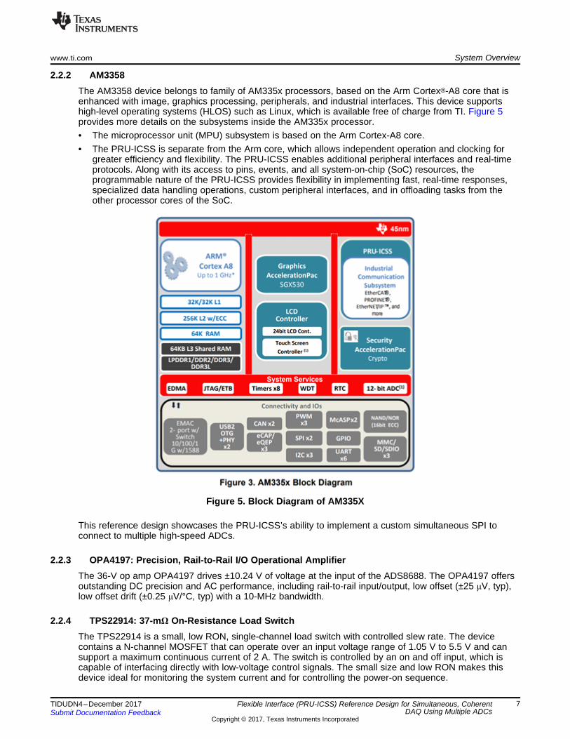
2.1 Block DiagramThis reference design consists of the following subsystems:• Sensor boards connect outputs of current transformers (CTs) and potential transformers (PTs) to the
data acquisition board.• The data acquisition board has six ADS8688 for supporting 48 channels taking inputs from sensor
boards. In addition, high voltage drivers (±10 V) are used to gain the signal.• A 5.5-V supply is used to derive all the voltage rails including ±12 V, +5 V, +3.3 V.• The adapter card acts as an intermediate interface to match the pin signals between the ADC and the
Sitara processor. A clock buffer is added to clean up the clock before fanning out to six ADCs.• The BeagleBone Black EVM is used as the host to demonstrate the working of PRU-ICSS.
Figure 3. Block Diagram of TIDA-01555

System Overview www.ti.com
6 TIDUDN4–December 2017Submit Documentation Feedback
Copyright © 2017, Texas Instruments Incorporated
Flexible Interface (PRU-ICSS) Reference Design for Simultaneous, CoherentDAQ Using Multiple ADCs
Figure 4 shows the interconnection between the ADCs and the Sitara processor. SDI and SDO pins are allconnected to individual GPO, GPI pins in PRU. All CS pins are tied to a single GPO pin for simultaneoussampling across ADCs. Each clock pin is driven by separate output lines from the clock buffer, whichtakes input from a single GPO pin of PRU.
Figure 4. Interconnection Between Six ADS8688s and PRU-ICSS
2.2 Highlighted Products
2.2.1 ADS8688: 500-kSPS, 8-Channel, SAR ADC With Bipolar Input RangesThe ADS8688 is an 8-channel, 16-bit successive approximation register (SAR) ADC capable of running at500 ksps. The ADC has an integrated front-end mux with automatic and manual scanning modes, an on-chip precision low drift reference, and ±20-V overvoltage protection. Each input channel on the device cansupport true bipolar input ranges of ±10.24 V, ±5.12 V, and ±2.56 V as well as unipolar input ranges of 0 Vto 10.24 V and 0 V to 5.12 V while operating on a 5-V unipolar supply. The gain of the analog front end(AFE) for all input ranges is accurately trimmed to ensure a high DC precision. The input range selectionis software-programmable and independently controlled for each channel. The device offers a 1-MΩconstant resistive input impedance irrespective of the selected input range.
The ADS8688 offers a simple SPI-compatible serial interface to the digital host and also support daisy-chaining of multiple devices. The digital supply operates from 1.65 V to 5.25 V, enabling direct interface toa wide range of host controllers. For more details on the features of the ADS8688, see ADS868xA 16-Bit,500-kSPS, 4- and 8-Channel, Single-Supply, SAR ADCs with Bipolar Input Ranges.
www.ti.com System Overview
7TIDUDN4–December 2017Submit Documentation Feedback
Copyright © 2017, Texas Instruments Incorporated
Flexible Interface (PRU-ICSS) Reference Design for Simultaneous, CoherentDAQ Using Multiple ADCs
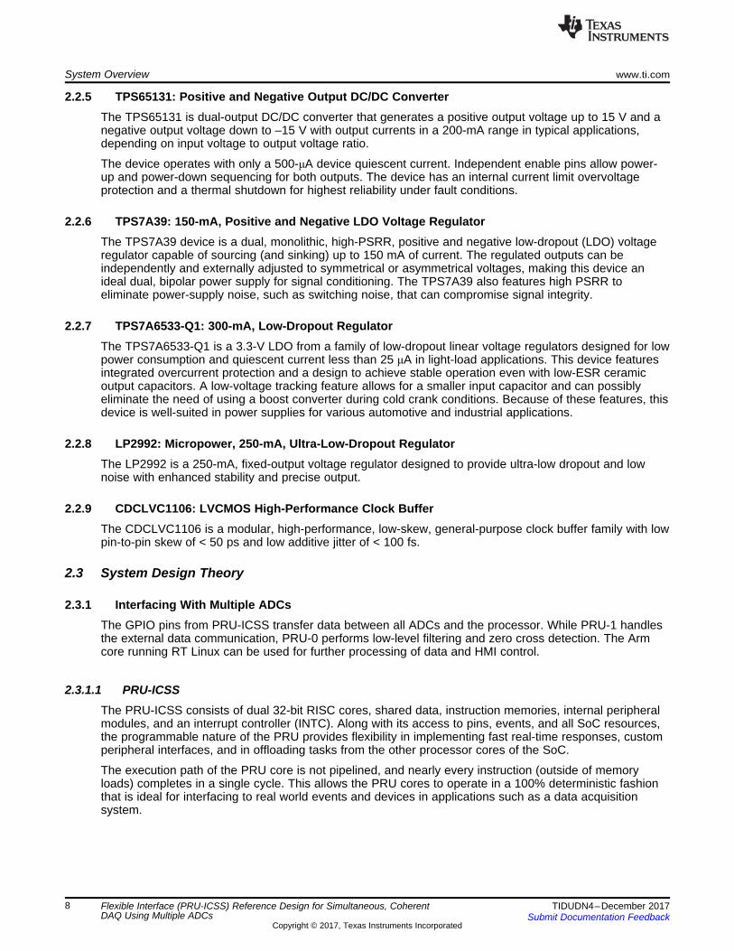
2.2.2 AM3358The AM3358 device belongs to family of AM335x processors, based on the Arm Cortex®-A8 core that isenhanced with image, graphics processing, peripherals, and industrial interfaces. This device supportshigh-level operating systems (HLOS) such as Linux, which is available free of charge from TI. Figure 5provides more details on the subsystems inside the AM335x processor.• The microprocessor unit (MPU) subsystem is based on the Arm Cortex-A8 core.• The PRU-ICSS is separate from the Arm core, which allows independent operation and clocking for
greater efficiency and flexibility. The PRU-ICSS enables additional peripheral interfaces and real-timeprotocols. Along with its access to pins, events, and all system-on-chip (SoC) resources, theprogrammable nature of the PRU-ICSS provides flexibility in implementing fast, real-time responses,specialized data handling operations, custom peripheral interfaces, and in offloading tasks from theother processor cores of the SoC.
Figure 5. Block Diagram of AM335X
This reference design showcases the PRU-ICSS’s ability to implement a custom simultaneous SPI toconnect to multiple high-speed ADCs.
2.2.3 OPA4197: Precision, Rail-to-Rail I/O Operational AmplifierThe 36-V op amp OPA4197 drives ±10.24 V of voltage at the input of the ADS8688. The OPA4197 offersoutstanding DC precision and AC performance, including rail-to-rail input/output, low offset (±25 μV, typ),low offset drift (±0.25 μV/°C, typ) with a 10-MHz bandwidth.
2.2.4 TPS22914: 37-mΩ On-Resistance Load SwitchThe TPS22914 is a small, low RON, single-channel load switch with controlled slew rate. The devicecontains a N-channel MOSFET that can operate over an input voltage range of 1.05 V to 5.5 V and cansupport a maximum continuous current of 2 A. The switch is controlled by an on and off input, which iscapable of interfacing directly with low-voltage control signals. The small size and low RON makes thisdevice ideal for monitoring the system current and for controlling the power-on sequence.
System Overview www.ti.com
8 TIDUDN4–December 2017Submit Documentation Feedback
Copyright © 2017, Texas Instruments Incorporated
Flexible Interface (PRU-ICSS) Reference Design for Simultaneous, CoherentDAQ Using Multiple ADCs
2.2.5 TPS65131: Positive and Negative Output DC/DC ConverterThe TPS65131 is dual-output DC/DC converter that generates a positive output voltage up to 15 V and anegative output voltage down to –15 V with output currents in a 200-mA range in typical applications,depending on input voltage to output voltage ratio.
The device operates with only a 500-μA device quiescent current. Independent enable pins allow power-up and power-down sequencing for both outputs. The device has an internal current limit overvoltageprotection and a thermal shutdown for highest reliability under fault conditions.
2.2.6 TPS7A39: 150-mA, Positive and Negative LDO Voltage RegulatorThe TPS7A39 device is a dual, monolithic, high-PSRR, positive and negative low-dropout (LDO) voltageregulator capable of sourcing (and sinking) up to 150 mA of current. The regulated outputs can beindependently and externally adjusted to symmetrical or asymmetrical voltages, making this device anideal dual, bipolar power supply for signal conditioning. The TPS7A39 also features high PSRR toeliminate power-supply noise, such as switching noise, that can compromise signal integrity.
2.2.7 TPS7A6533-Q1: 300-mA, Low-Dropout RegulatorThe TPS7A6533-Q1 is a 3.3-V LDO from a family of low-dropout linear voltage regulators designed for lowpower consumption and quiescent current less than 25 μA in light-load applications. This device featuresintegrated overcurrent protection and a design to achieve stable operation even with low-ESR ceramicoutput capacitors. A low-voltage tracking feature allows for a smaller input capacitor and can possiblyeliminate the need of using a boost converter during cold crank conditions. Because of these features, thisdevice is well-suited in power supplies for various automotive and industrial applications.
2.2.8 LP2992: Micropower, 250-mA, Ultra-Low-Dropout RegulatorThe LP2992 is a 250-mA, fixed-output voltage regulator designed to provide ultra-low dropout and lownoise with enhanced stability and precise output.
2.2.9 CDCLVC1106: LVCMOS High-Performance Clock BufferThe CDCLVC1106 is a modular, high-performance, low-skew, general-purpose clock buffer family with lowpin-to-pin skew of < 50 ps and low additive jitter of < 100 fs.
2.3 System Design Theory
2.3.1 Interfacing With Multiple ADCsThe GPIO pins from PRU-ICSS transfer data between all ADCs and the processor. While PRU-1 handlesthe external data communication, PRU-0 performs low-level filtering and zero cross detection. The Armcore running RT Linux can be used for further processing of data and HMI control.
2.3.1.1 PRU-ICSSThe PRU-ICSS consists of dual 32-bit RISC cores, shared data, instruction memories, internal peripheralmodules, and an interrupt controller (INTC). Along with its access to pins, events, and all SoC resources,the programmable nature of the PRU provides flexibility in implementing fast real-time responses, customperipheral interfaces, and in offloading tasks from the other processor cores of the SoC.
The execution path of the PRU core is not pipelined, and nearly every instruction (outside of memoryloads) completes in a single cycle. This allows the PRU cores to operate in a 100% deterministic fashionthat is ideal for interfacing to real world events and devices in applications such as a data acquisitionsystem.
MII0 RX / TX
PRU0 Core8 KB IRAM
Scratch 0/1/2
PRU1 Core8 KB IRAM
MII1 RX / TX
UART
SD / FB
Interrupt Controller
Industrial Ethernet
16 GPI16 GPO
Oversampled Shift
Industrial Fieldbus
9 Channel SD filter3 channel pos feedback
Interrupts to ARM / DSP INTCEvents from Peripherals + PRUs
Industrial Ethernet
16 GPI16 GPO
Oversampled Shift
32-bit Interconnect SC
R
DRAM0(8KB)
DRAM1(8KB)
Shared(12KB)
CRC 16/32
Master I/F (to SCR)
Slave I/F (to SCR)
IEP
eCAP
MAC
www.ti.com System Overview
9TIDUDN4–December 2017Submit Documentation Feedback
Copyright © 2017, Texas Instruments Incorporated
Flexible Interface (PRU-ICSS) Reference Design for Simultaneous, CoherentDAQ Using Multiple ADCs
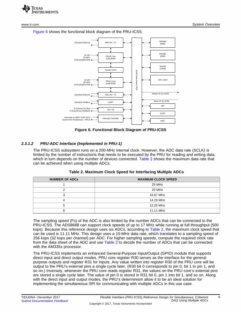
Figure 6 shows the functional block diagram of the PRU-ICSS.
Figure 6. Functional Block Diagram of PRU-ICSS
2.3.1.2 PRU-ADC Interface (Implemented in PRU-1)The PRU-ICSS subsystem runs on a 200-MHz internal clock. However, the ADC data rate (SCLK) islimited by the number of instructions that needs to be executed by the PRU for reading and writing data,which in turn depends on the number of devices connected. Table 2 shows the maximum data rate thatcan be achieved when using multiple ADCs.
Table 2. Maximum Clock Speed for Interfacing Multiple ADCs
NUMBER OF ADCs MAXIMUM CLOCK SPEED1 25 MHz2 20 MHz3 16.67 MHz4 14.29 MHz5 12.25 MHz6 11.11 MHz
The sampling speed (Fs) of the ADC is also limited by the number ADCs that can be connected to thePRU-ICSS. The ADS8688 can support clock speeds of up to 17 MHz while running at full throughput (500ksps). Because this reference design uses six ADCs, according to Table 2, the maximum clock speed thatcan be used is 11.11 MHz. This design uses a 10-MHz data rate, which translates to a sampling speed of256 ksps (32 ksps per channel) per ADC. For higher sampling speeds, compute the required clock ratefrom the data sheet of the ADC and use Table 2 to decide the number of ADCs that can be connectedwith the AM335x processor.
The PRU-ICSS implements an enhanced General-Purpose Input/Output (GPIO) module that supportsdirect input and direct output modes. PRU core register R30 serves as the interface for the generalpurpose outputs and register R31 for inputs. Any value written into register R30 of the PRU core will beoutput to the PRU’s external pins a single cycle later. (R30 bit 0 corresponds to pin 0, bit 1 to pin 1, andso on.) Inversely, whenever the PRU core reads register R31, the values on the PRU core’s external pinsare stored a single cycle later. The value of pin 0 is stored in R31 bit 0, pin 1 into bit 1, and so on. Alongwith the direct input and output modes, the PRU’s determinism allow it to be an ideal solution forimplementing the simultaneous SPI for communicating with multiple ADCs in this use case.

GPO[R30]
CS
CLK
MOSI 0
MOSI n
MOSI5
GPI[R30]
MISO 0
MISO n
MISO 5
PRUCore
ADC 0 Config Chan N-1 ADC 0 Config Chan N
ADC n Config Chan N
ADC 5 Config Chan N
ADC 0 Channel N Data
ADC n Channel N Data
ADC 5 Channel N Data
ADC n Config Chan N-1
ADC 5 Config Chan N-1
System Overview www.ti.com
10 TIDUDN4–December 2017Submit Documentation Feedback
Copyright © 2017, Texas Instruments Incorporated
Flexible Interface (PRU-ICSS) Reference Design for Simultaneous, CoherentDAQ Using Multiple ADCs
Figure 7 shows the simultaneous SPI that has been configured in the PRU software. Shared chip selectand SPI clock allow ADCs to acquire data simultaneously and at the same instance. Each ADC devicehas its own MISO and MOSI pins so that the ADC configurations and data can be sent and received inparallel.
Figure 7. Interfacing Between ADC and PRU
2.3.1.2.1 Advantages of Using PRU-ICSSThis subsection showcases the benefits of using bit-banging in PRU-ICSS over dedicated hardware SPIperipheral.
Table 3. Advantages of PRU-ICSS
PARAMETER SPI PRU-ICSS
Connections to slave Fixed (1, 2, 4); depends on the product familySPI offering
Variable (1, 2, 3..n); depends on the configurationson the PRU GPIO
Flexibility with controllingthe CS
If each SPI port has a dedicated CS then thephase delay between different SPI ports couldintroduce error in simultaneous sampling.
CS is an independent timing signal and hence cancontrol all ADCs simultaneously with one commonsignal.
System bandwidth
More frequent CPU core interrupt as it needsto manage the DMA allocation and datatransfer between SPI ports, memory, CPU dueto shared resources.
CPU core interrupt is no longer required as bothPRUs can run independently.
This limits the overall sampling speed of ADCswhen multiple SPI ports are used.
ADCs can run at higher sampling speed as the datais now transferred at much faster rate betweenmultiple ADCs and PRU.
The CPU core cannot do any data computationin parallel when being used for supervisoryfunction.
The CPU core is now idle as second PRU is usedfor ZCD. The core can be used for post processingof data or for implementing other functionalities.
Timing compensation
In SPI peripherals, the relationship betweenclock edge and the arrival of data has to betightly controlled (less than half CLK cycle). Athigher speeds or with digital isolators, signalpath delays could be significant to affect thetiming criteria. This results in corrupted datathat requires expensive hardware fixes orreduced throughput.
The PRU-ICSS subsystem is more relaxed as thedelays in arrival of data beyond the CLK edge canbe compensated due to a higher resolution internaltime base (5 ns) for data capture.
2.3.1.3 Digital Filtering and Feedback (Implemented in PRU-0)The simultaneous SPI interface is accomplished in only one of the two PRU cores in the PRU-ICSS. Thisfrees up the other PRU core to provide a feedback loop for the incoming signal frequency (to adjust theADC sampling rate for achieving coherent sampling) as well as perform low-level filtering on the incomingADC data. Because the timing requirements on this PRU core is not as tight, the firmware is implementedin C code.
www.ti.com System Overview
11TIDUDN4–December 2017Submit Documentation Feedback
Copyright © 2017, Texas Instruments Incorporated
Flexible Interface (PRU-ICSS) Reference Design for Simultaneous, CoherentDAQ Using Multiple ADCs
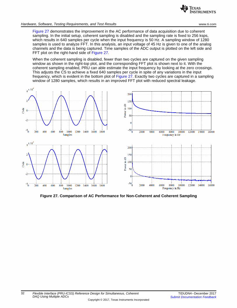
2.3.1.3.1 Coherent Sampling (Sample Rate Adjustment)When measuring periodic signals, such as voltage and current in an AC system, it is important to acquirea fixed number of samples per cycle. When the frequency of the line cycle changes, sampling rate of theADC is adjusted to maintain a fixed number of samples per cycle using a phase-locked loop circuit. Ingrid, methodology and admissible error that occur while measuring harmonic component is captured inIEC 61000-4-7. There are many ways of implementing PLL that could be done in either analog domain ordigital domain. Non-coherent sampling results in spectral leakages leading to loss of data and reduction inaccuracy as shown in Figure 27.
In this reference design, the second PRU core performs frequency estimation by using a zero crossdetection (ZCD) algorithm. Once the incoming frequency has been determined, the PRU can update thesampling rate of the acquisition PRU to achieve a precise number of samples per cycle across the fullrange of expected incoming frequencies (45 to 55 Hz). The ADC channel to be used for frequencyestimation, as well as the number of cycles are both configurable in the PRU firmware.
In Figure 27, a 45-Hz sine wave is provided to the ADC input. The top data is acquired at a fixed rate of32000 samples per second (assuming a 50-Hz input signal and 640 samples per cycle). For the bottomdata, the PRU is allowed to estimate the incoming signal frequency and then alter the sampling rate toachieve 640 samples per cycle. Notice that 1280 samples are exactly 2 periods of the signal and the FFTleakage rolls off very quickly in the bottom data.
2.3.1.3.2 Achievable Sampling FrequenciesEach PRU core in the PRU-ICSS runs at 200 MHz giving a cycle time of 5 ns. As mentioned before, theabsolute determinism of the PRU cores allows the developer to control what happens on each and everycycle. Knowing this, the ADC sampling frequency can be determined which the PRU can achieve for eachchannel.
Before digging into the frequencies, a discussion on the use case requirements and techniques used toaccomplish those requirements will be useful. This reference design has the following requirements:• 45- to 55-Hz incoming frequency: Assumed frequency is 50 Hz with a worst case variation of ±10%• 640 samples per cycle: Sampling rate must vary from 28.8 ksps to 35.2 ksps based on incoming
frequency• 10-MHz SPI clock• 48 ADC channels: Six ADCs are sampled in parallel, each with eight channels sampled sequentially
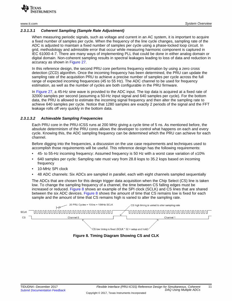
The ADCs that are chosen for this design trigger data acquisition when the Chip Select (CS) line is takenlow. To change the sampling frequency of a channel, the time between CS falling edges must beincreased or reduced. Figure 8 shows an example of the SPI clock (SCLK) and CS lines that are sharedbetween the six ADC devices. Figure 8 shows the amount of time that CS remains low is fixed for eachsample and the amount of time that CS remains high is varied to alter the sampling rate.
Figure 8. Timing Diagram Showing CS and CLK
System Overview www.ti.com
12 TIDUDN4–December 2017Submit Documentation Feedback
Copyright © 2017, Texas Instruments Incorporated
Flexible Interface (PRU-ICSS) Reference Design for Simultaneous, CoherentDAQ Using Multiple ADCs
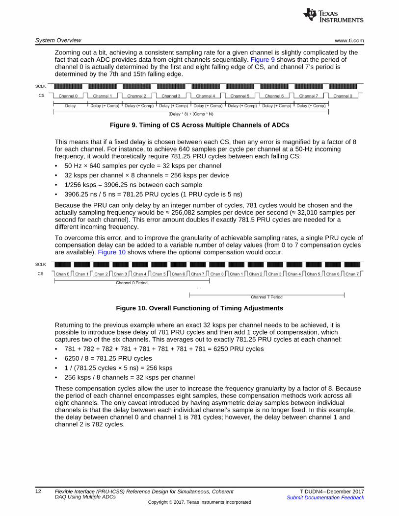
Zooming out a bit, achieving a consistent sampling rate for a given channel is slightly complicated by thefact that each ADC provides data from eight channels sequentially. Figure 9 shows that the period ofchannel 0 is actually determined by the first and eight falling edge of CS, and channel 7’s period isdetermined by the 7th and 15th falling edge.
Figure 9. Timing of CS Across Multiple Channels of ADCs
This means that if a fixed delay is chosen between each CS, then any error is magnified by a factor of 8for each channel. For instance, to achieve 640 samples per cycle per channel at a 50-Hz incomingfrequency, it would theoretically require 781.25 PRU cycles between each falling CS:• 50 Hz × 640 samples per cycle = 32 ksps per channel• 32 ksps per channel × 8 channels = 256 ksps per device• 1/256 ksps = 3906.25 ns between each sample• 3906.25 ns / 5 ns = 781.25 PRU cycles (1 PRU cycle is 5 ns)
Because the PRU can only delay by an integer number of cycles, 781 cycles would be chosen and theactually sampling frequency would be ≈ 256,082 samples per device per second (≈ 32,010 samples persecond for each channel). This error amount doubles if exactly 781.5 PRU cycles are needed for adifferent incoming frequency.
To overcome this error, and to improve the granularity of achievable sampling rates, a single PRU cycle ofcompensation delay can be added to a variable number of delay values (from 0 to 7 compensation cyclesare available). Figure 10 shows where the optional compensation would occur.
Figure 10. Overall Functioning of Timing Adjustments
Returning to the previous example where an exact 32 ksps per channel needs to be achieved, it ispossible to introduce base delay of 781 PRU cycles and then add 1 cycle of compensation, whichcaptures two of the six channels. This averages out to exactly 781.25 PRU cycles at each channel:• 781 + 782 + 782 + 781 + 781 + 781 + 781 + 781 = 6250 PRU cycles• 6250 / 8 = 781.25 PRU cycles• 1 / (781.25 cycles × 5 ns) = 256 ksps• 256 ksps / 8 channels = 32 ksps per channel
These compensation cycles allow the user to increase the frequency granularity by a factor of 8. Becausethe period of each channel encompasses eight samples, these compensation methods work across alleight channels. The only caveat introduced by having asymmetric delay samples between individualchannels is that the delay between each individual channel’s sample is no longer fixed. In this example,the delay between channel 0 and channel 1 is 781 cycles; however, the delay between channel 1 andchannel 2 is 782 cycles.

www.ti.com System Overview
13TIDUDN4–December 2017Submit Documentation Feedback
Copyright © 2017, Texas Instruments Incorporated
Flexible Interface (PRU-ICSS) Reference Design for Simultaneous, CoherentDAQ Using Multiple ADCs
After discussing the requirements and the techniques, the achievable sampling rates using theaforementioned methods can be shown. Table 4 covers the extremes of the input frequency range as wellas the expected middle. This is meant to show the best, worst, and average cases. Notice that theresolution between the ideal input frequency at each sampling rate never exceeds 0.01 Hz.
Table 4. Achievable Sampling Rates
DELAY CYCLES(5 ns)
COMPENSATION CYCLES (5
ns)
SAMPLING RATEPER CHANNEL
(sps)SAMPLING RATEPER DEVICE (sps)
IDEAL FREQUENCYAT SAMPLING RATE
(Hz)
RESOLUTIONFROM NEXTFREQUENCY
(Hz)710 0 35211.2676 281690.1408 55.0176 0.00968710 1 35205.0695 281640.5562 55.0079 0.00968710 2 35198.8736 281590.9891 54.9982 0.00968710 3 35192.6799 281541.4394 54.9886 0.00967710 4 35186.4884 281491.9071 54.9789 0.00967710 5 35180.2990 281442.3923 54.9692 0.00967710 6 35174.1119 281392.8948 54.9595 0.00966710 7 35167.9269 281343.4148 54.9499 0.00966
… … … … … …781 0 32010.2433 256081.9462 50.0160 0.00800781 1 32005.1208 256040.9666 50.0080 0.00800781 2 32000.0000 256000.0000 50.0000 0.00800781 3 31994.8808 255959.0466 49.9920 0.00800781 4 31989.7633 255918.1062 49.9840 0.00799781 5 31984.6474 255877.1790 49.9760 0.00799781 6 31979.5331 255836.2648 49.9680 0.00799781 7 31974.4205 255795.3637 49.9600 0.00799
… … … … … …868 0 28801.8433 230414.7465 45.0029 0.00648868 1 28797.6962 230381.5695 44.9964 0.00648868 2 28793.5502 230348.4020 44.9899 0.00648868 3 28789.4055 230315.2440 44.9834 0.00647868 4 28785.2619 230282.0956 44.9770 0.00647868 5 28781.1196 230248.9567 44.9705 0.00647868 6 28776.9784 230215.8273 44.9640 0.00647868 7 28772.8384 230182.7075 44.9576 0.00647
2.3.1.3.3 OversamplingDigital domain filtering is also performed by the second PRU in the form of an averaging filter. This filterachieves the same results as the oversampling function on more expensive ADCs. Oversampling theincoming data performs a low-pass filter and removes high-frequency noise before passing the data on tothe next stop in the processing pipeline. The PRU core accumulates the samples from each channel asthe data is coming in and then once the configurable oversampling factor is reached the division isperformed to get the average value.
2.3.1.4 High-Level Data Processing (Implemented in Arm Core)All of the data acquisition and low-level processing happens completely in the PRU-ICSS without requiringa single cycle from the Arm core. This allows the Arm core to focus on higher level processing andcommunications. In this reference design, the Arm core is running Texas Instrument’s Processor SDK RTLinux distribution. This distribution of Linux comes with the PREEMPT_RT patch applied and allows foruser space threads to be assigned priorities that can allow them to get (nearly) uninterrupted CPU cyclesfor short periods of time.
System Overview www.ti.com
14 TIDUDN4–December 2017Submit Documentation Feedback
Copyright © 2017, Texas Instruments Incorporated
Flexible Interface (PRU-ICSS) Reference Design for Simultaneous, CoherentDAQ Using Multiple ADCs
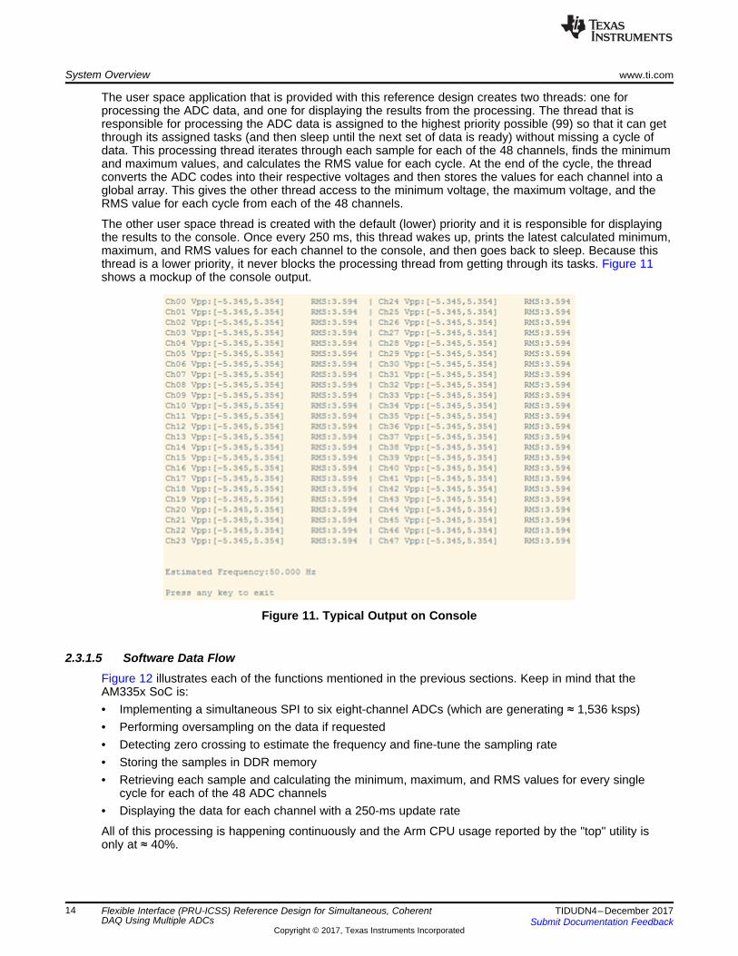
The user space application that is provided with this reference design creates two threads: one forprocessing the ADC data, and one for displaying the results from the processing. The thread that isresponsible for processing the ADC data is assigned to the highest priority possible (99) so that it can getthrough its assigned tasks (and then sleep until the next set of data is ready) without missing a cycle ofdata. This processing thread iterates through each sample for each of the 48 channels, finds the minimumand maximum values, and calculates the RMS value for each cycle. At the end of the cycle, the threadconverts the ADC codes into their respective voltages and then stores the values for each channel into aglobal array. This gives the other thread access to the minimum voltage, the maximum voltage, and theRMS value for each cycle from each of the 48 channels.
The other user space thread is created with the default (lower) priority and it is responsible for displayingthe results to the console. Once every 250 ms, this thread wakes up, prints the latest calculated minimum,maximum, and RMS values for each channel to the console, and then goes back to sleep. Because thisthread is a lower priority, it never blocks the processing thread from getting through its tasks. Figure 11shows a mockup of the console output.
Figure 11. Typical Output on Console
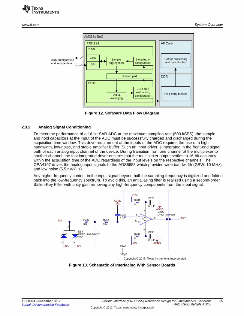
2.3.1.5 Software Data FlowFigure 12 illustrates each of the functions mentioned in the previous sections. Keep in mind that theAM335x SoC is:• Implementing a simultaneous SPI to six eight-channel ADCs (which are generating ≈ 1,536 ksps)• Performing oversampling on the data if requested• Detecting zero crossing to estimate the frequency and fine-tune the sampling rate• Storing the samples in DDR memory• Retrieving each sample and calculating the minimum, maximum, and RMS values for every single
cycle for each of the 48 ADC channels• Displaying the data for each channel with a 250-ms update rate
All of this processing is happening continuously and the Arm CPU usage reported by the "top" utility isonly at ≈ 40%.
8
10
9
CV+
V-
411
U28COPA4197IPWR
0.1µF
C228
0.1µF
C238
+12V
-12V
AGND
AGND
51k
R253
51k
R25447pFC230
100pF
C240
AGND
F0+
1
3
2
70V
D54DESD1P0RFWQ-7
-12V +12V
FO0+
0
R334
0
R336
Copyright © 2017, Texas Instruments Incorporated
GPO
GPI
Sampleaggregation
Sampling orconfiguration
Scratch pad
PRU1
ZCD, freq estimation,
configuration
PRU0
Digital averagingDigital
averaging
PRUSS1
Further processingand data display
A8 Core
Ping-pong buffers
DDR
AM335x SoC
ADC configuration and sample data
www.ti.com System Overview
15TIDUDN4–December 2017Submit Documentation Feedback
Copyright © 2017, Texas Instruments Incorporated
Flexible Interface (PRU-ICSS) Reference Design for Simultaneous, CoherentDAQ Using Multiple ADCs
Figure 12. Software Data Flow Diagram
2.3.2 Analog Signal ConditioningTo meet the performance of a 16-bit SAR ADC at the maximum sampling rate (500 kSPS), the sampleand hold capacitors at the input of the ADC must be successfully charged and discharged during theacquisition-time window. This drive requirement at the inputs of the ADC requires the use of a highbandwidth, low-noise, and stable amplifier buffer. Such an input driver is integrated in the front-end signalpath of each analog input channel of the device. During transition from one channel of the multiplexer toanother channel, the fast integrated driver ensures that the multiplexer output settles to 16-bit accuracywithin the acquisition time of the ADC regardless of the input levels on the respective channels. TheOPA4197 drives the analog input signals to the ADS8688 which provides wide bandwidth (GBW: 10 MHz)and low noise (5.5 nV/√Hz).
Any higher frequency content in the input signal beyond half the sampling frequency is digitized and foldedback into the low-frequency spectrum. To avoid this, an antialiasing filter is realized using a second-orderSallen-Key Filter with unity gain removing any high-frequency components from the input signal.
Figure 13. Schematic of Interfacing With Sensor Boards
SDI1
RST/PD2
DAISY3
REFSEL4
REFIO5
REFGND6
REFCAP7
AGND8
AVDD9
AUX_IN10
AUX_GND11
AIN_6P12
AIN_6GND13
AIN_7P14
AIN_7GND15
AIN_0P16
AIN_0GND17
AIN_1P18
AIN_1GND19
AIN_2GND20
AIN_2P21
AIN_3GND22
AIN_3P23
AIN_4GND24
AIN_4P25
AIN_5GND26
AIN_5P27
AGND28
AGND29
AVDD30
AGND31
AGND32
DGND33
DVDD34
DNC35
SDO36
SCLK37
CS38
U14
ADS8688IDBT
AGND
DGND
SDI_2
CS2
SCLK_2
1µF
C80
0.1µF
C82
10µF
C81
1µF
C83
0.1µF
C85
10µF
C84
22µF
C100
1µF
C101
47.0kR88
47.0k R95
+3.3V
+5V
AGND DGND
+3.3V
10µF
C99
AGND
0.01µFC90
0.01µFC91
0.01µFC94
0.01µFC95
0.01µFC96
0.01µFC102
0.01µFC103
0.01µFC104
357R85
357R86
357R87
357R89
357 R94
357R99
357R96
357R100
357R105
357R106
357 R103
357R104
357 R101
357R102
357 R97357R98
B0-
B1-
B2-
B3-
B4-
B5-
B6-
B7-
BO4+
BO5+
BO6+
BO7+
BO3+
BO2+
BO1+
BO0+
0R301
0R300
+5V
+3.3V
DGND
0.1µF
C267
SDO_2
+3.3V
DGND
2 4
53
U32
SN74LVC1G17DCKR
DGND
AGND
0R318
Copyright © 2017, Texas Instruments Incorporated
System Overview www.ti.com
16 TIDUDN4–December 2017Submit Documentation Feedback
Copyright © 2017, Texas Instruments Incorporated
Flexible Interface (PRU-ICSS) Reference Design for Simultaneous, CoherentDAQ Using Multiple ADCs
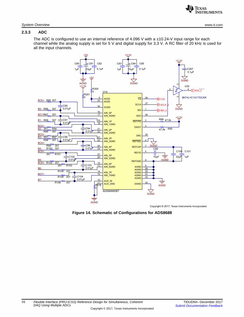
2.3.3 ADCThe ADC is configured to use an internal reference of 4.096 V with a ±10.24-V input range for eachchannel while the analog supply is set for 5 V and digital supply for 3.3 V. A RC filter of 20 kHz is used forall the input channels.
Figure 14. Schematic of Configurations for ADS8688
CLKIN1
1G2
Y03
GND4
VDD5
Y46
GND7
VDD8
Y59
GND10
Y211
VDD12
Y313
Y114
U1
CDCLVC1106PWR
DGND
+3.3V
SCLK_16
10µFC1
0.1µFC2
DGND
1000 ohm
FB1
1µFC3
SCLK_4
SCLK_5
SCLK_1
SCLK_6
SCLK_2
SCLK_3
0
R1
0
R2
0
R3
0
R4
0
R5
0
R6
Copyright © 2017, Texas Instruments Incorporated
CS1
CS2
CS3
CS4
CS5
CS6
24
53
U2SN74LVC1G17DCKR
0.1µFC4
+3.3V
DGND
DGND
CS1to6
Copyright © 2017, Texas Instruments Incorporated
www.ti.com System Overview
17TIDUDN4–December 2017Submit Documentation Feedback
Copyright © 2017, Texas Instruments Incorporated
Flexible Interface (PRU-ICSS) Reference Design for Simultaneous, CoherentDAQ Using Multiple ADCs
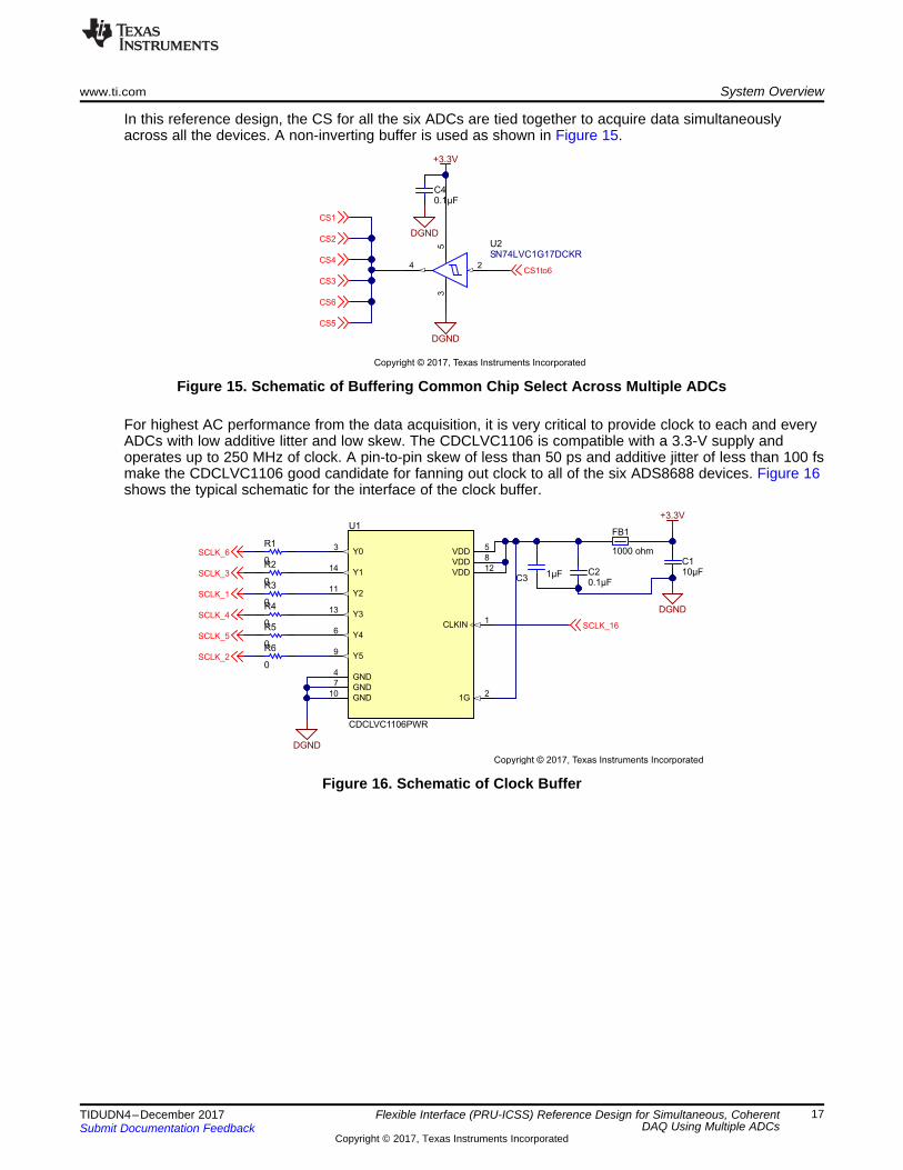
In this reference design, the CS for all the six ADCs are tied together to acquire data simultaneouslyacross all the devices. A non-inverting buffer is used as shown in Figure 15.
Figure 15. Schematic of Buffering Common Chip Select Across Multiple ADCs
For highest AC performance from the data acquisition, it is very critical to provide clock to each and everyADCs with low additive litter and low skew. The CDCLVC1106 is compatible with a 3.3-V supply andoperates up to 250 MHz of clock. A pin-to-pin skew of less than 50 ps and additive jitter of less than 100 fsmake the CDCLVC1106 good candidate for fanning out clock to all of the six ADS8688 devices. Figure 16shows the typical schematic for the interface of the clock buffer.
Figure 16. Schematic of Clock Buffer

Load SwitchTPS22914
LDOTPS7A6533
LDOLP2992
DC/DC converter
TPS65131
Voltage supply
5.5 V LDOTPS7A39
14 V
±14 V
12 V
±12 V
AVcc
AVDD:5V
Copyright © 2017, Texas Instruments Incorporated
System Overview www.ti.com
18 TIDUDN4–December 2017Submit Documentation Feedback
Copyright © 2017, Texas Instruments Incorporated
Flexible Interface (PRU-ICSS) Reference Design for Simultaneous, CoherentDAQ Using Multiple ADCs
2.3.4 Power SupplyAnalog signal conditioning and data conversion require a power supply with multiple voltage levels. TheADS8688 requires a 5-V supply at the AVDD and uses 3.3 V for the digital interface at DVDD pin.• 5-V AVDD: The ADS8688 requires a maximum of 16 mA at the 5-V supply and for maximum data
throughput. For six ADCs, the total current requirement is approximately 96 mA.• 3.3-V DVDD: Dynamic digital requirement for the current supply is typically 0.5 mA for one ADS8688
device. Including the digital buffer and LED indicators, the overall supply current required is around 50mA.
• ±12-V AVcc: This is required to power up the AFE to condition the input signals feeding to ADCs. TheOPA4197 drive the input signals and needs up to 1.5 mA per amplifier summing up to 72 mA for all the48 channels.Based on these power requirements, the power tree for the system is designed as shown in Figure 17.
• Load switch: This is used at the front end of the power supply to disable power supply to the wholeboard when OE is deactivated. OE is a GPIO connected to the Sitara processor to enable and powerup the data acquisition board. This connection helps prevent any GPIO from getting pulled high or lowwhen Sitara is not powered up providing fail-safe operation.
A single supply of 5.5 V is used to derive multiple voltage levels using power converters and LDOs asshown in Figure 17. The TPS65131 generates both positive and negative voltage outputs from a singlesupply. This converter has internal boost converter control to step up the input voltage and an invertingconverter control to derive negative voltage. External passives are designed to obtain ±14 V from theinput.
Figure 17. Power Tree for Data Acquisition
INP1
EN2
NR/SS3
GND4
INN5
OUTN6
FBN 7
BUF8
FBP9
OUTP10
PAD11
U8
TPS7A3901DS C
2.2µFC64
274kR60
31.6kR63
2.2µFC66
274kR62
27.4kR66
1µFC63
10µFC62
+14V
1µFC69
10µFC68
- 14V
0R65
+14V
0.01µF
C67
0.1µF
C61
0.1µFC65
0
R58
0
R67
-12V
+12V
0R59
0R61AGND
AGND
AGND
AGND
AGNDAGND
AGND
TP7
TP8
15V21
D11DZ2W15000L
AGND
15V
21
D14DZ2W15000L
AGND
Copyright © 2017, Texas Instruments Incorporated
INP1
PGND2
PGND3
VIN4
INN5
INN6
BSW7
ENP8
PSP9
ENN10
PSN11
NC12
OUTN13
OUTN14
VNEG15
FBN16
VREF17
CN18
AGND19
NC20
CP21
FBP22
VPOS23
INP24
PP25
U7
TPS65131RGET
4.7µFC47
4.7µFC56
1.00
R56
+5V_IN
1µFC55
D15
MBRM120ET1G
4.7µFC57
4.7µFC58
4.7µFC59
10pF
C52
49.9k
R5549.9k
R54 620k
R52
0
R53
4.7µFC54
0
R51
1.0k
R57
10pFC50
4.7µFC43
4.7µFC44
4.7µFC45 4.7µF
C42
0.1µFC53
0
R46
0.01µFC46
0.01µFC51
0.01µFC60
0.22µF
C49
D10
MBRM120ET1G
+14V
-14V
SH-J1
J2
SH-J2
J4INPUT VOLTAGE: +5.5V
AGND
AGND AGND
AGNDAGND
AGND
AGND
AGND
AGND
VOUTA1
VINA2
GNDB1
ONB2
U5
TPS22914YFP
+5V_IN
AGNDON
V_IN
1
3
2
1AJ3
PJ-002AH-SMT-TR
TP5 TP4
TP2
4.7µHL2
4.7µH
L1
576k
R49
0R47
49.9k
R50
1 2
J11
PEC02SAAN
AGND
1 2
J12
PEC02SAAN
AGND
1µF
C272
AGND
0.1µF
C273
Copyright © 2017, Texas Instruments Incorporated
www.ti.com System Overview
19TIDUDN4–December 2017Submit Documentation Feedback
Copyright © 2017, Texas Instruments Incorporated
Flexible Interface (PRU-ICSS) Reference Design for Simultaneous, CoherentDAQ Using Multiple ADCs
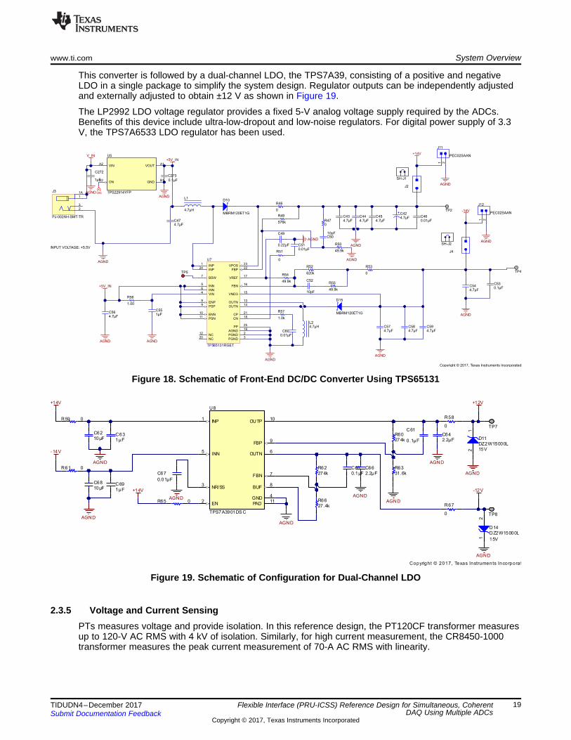
This converter is followed by a dual-channel LDO, the TPS7A39, consisting of a positive and negativeLDO in a single package to simplify the system design. Regulator outputs can be independently adjustedand externally adjusted to obtain ±12 V as shown in Figure 19.
The LP2992 LDO voltage regulator provides a fixed 5-V analog voltage supply required by the ADCs.Benefits of this device include ultra-low-dropout and low-noise regulators. For digital power supply of 3.3V, the TPS7A6533 LDO regulator has been used.
Figure 18. Schematic of Front-End DC/DC Converter Using TPS65131
Figure 19. Schematic of Configuration for Dual-Channel LDO
2.3.5 Voltage and Current SensingPTs measures voltage and provide isolation. In this reference design, the PT120CF transformer measuresup to 120-V AC RMS with 4 kV of isolation. Similarly, for high current measurement, the CR8450-1000transformer measures the peak current measurement of 70-A AC RMS with linearity.
BeagleBone Black EVM
Sensor board
Analog signal conditioning interface
Hardware, Software, Testing Requirements, and Test Results www.ti.com
20 TIDUDN4–December 2017Submit Documentation Feedback
Copyright © 2017, Texas Instruments Incorporated
Flexible Interface (PRU-ICSS) Reference Design for Simultaneous, CoherentDAQ Using Multiple ADCs
3 Hardware, Software, Testing Requirements, and Test ResultsThis section provides information on connecting this reference design for functional and performancetesting.
3.1 Required Hardware and Software
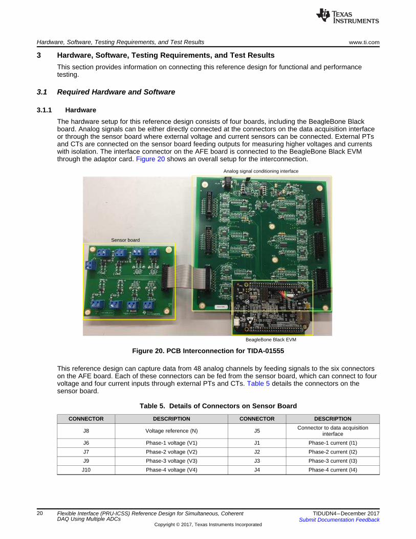
3.1.1 HardwareThe hardware setup for this reference design consists of four boards, including the BeagleBone Blackboard. Analog signals can be either directly connected at the connectors on the data acquisition interfaceor through the sensor board where external voltage and current sensors can be connected. External PTsand CTs are connected on the sensor board feeding outputs for measuring higher voltages and currentswith isolation. The interface connector on the AFE board is connected to the BeagleBone Black EVMthrough the adaptor card. Figure 20 shows an overall setup for the interconnection.
Figure 20. PCB Interconnection for TIDA-01555
This reference design can capture data from 48 analog channels by feeding signals to the six connectorson the AFE board. Each of these connectors can be fed from the sensor board, which can connect to fourvoltage and four current inputs through external PTs and CTs. Table 5 details the connectors on thesensor board.
Table 5. Details of Connectors on Sensor Board
CONNECTOR DESCRIPTION CONNECTOR DESCRIPTION
J8 Voltage reference (N) J5 Connector to data acquisitioninterface
J6 Phase-1 voltage (V1) J1 Phase-1 current (I1)J7 Phase-2 voltage (V2) J2 Phase-2 current (I2)J9 Phase-3 voltage (V3) J3 Phase-3 current (I3)J10 Phase-4 voltage (V4) J4 Phase-4 current (I4)

www.ti.com Hardware, Software, Testing Requirements, and Test Results
21TIDUDN4–December 2017Submit Documentation Feedback
Copyright © 2017, Texas Instruments Incorporated
Flexible Interface (PRU-ICSS) Reference Design for Simultaneous, CoherentDAQ Using Multiple ADCs
Table 6 details the connectors on the AFE board where analog inputs for all the 48 channels can be given.This board can be operated from a single power supply of 5.5 V at the connector J3. There is a provisionto supply an external ±14 V for the data acquisition card.
Table 6. Connector Details for Data Acquisition Board
CONNECTOR DESCRIPTION CONNECTOR DESCRIPTIONJ1 Signals from Sensor Board-1 J3 Power supply inputJ6 Signals from Sensor Board-2 J5 Connector to adaptor boardJ7 Signals from Sensor Board-3 J11 Option for external 14-V supplyJ8 Signals from Sensor Board-4 J12 Option for external –14-V supplyJ9 Signals from Sensor Board-5 J10 Signals from Sensor Board-6
This reference design provides multiple test points for probing the voltages at different stages fordebugging purposes. Table 7 lists the different available test points.
Table 7. Test Points on Data Acquisition Board
TEST POINTS DESCRIPTION TEST POINTS DESCRIPTIONTP1 5-V AVDD TP5 Pin for external battery switchTP2 14 V TP6 3.3-V DVDDTP3 AGND TP7 12 VTP4 –14 V TP8 –12 V
Analog inputs for an individual ADS8688 is mapped onto separate connectors with a provision for feedingdifferential analog signal for all the eight inputs of the ADC as given in Table 8.
Table 8. Connector Interfacing Sensor Board and AFE Board
PIN NO DESCRIPTION PIN NO DESCRIPTION1 AIN5+ 2 AIN5-3 AIN4+ 4 AIN4-5 AIN3+ 6 AIN3-7 AIN2+ 8 AIN2-9 AIN1+ 10 AIN1-11 AIN0+ 12 AIN0-13 AIN7+ 14 AIN7-15 AIN6+ 16 AIN6-17 AGND 18 AGND19 12 V 20 –12 V
Hardware, Software, Testing Requirements, and Test Results www.ti.com
22 TIDUDN4–December 2017Submit Documentation Feedback
Copyright © 2017, Texas Instruments Incorporated
Flexible Interface (PRU-ICSS) Reference Design for Simultaneous, CoherentDAQ Using Multiple ADCs
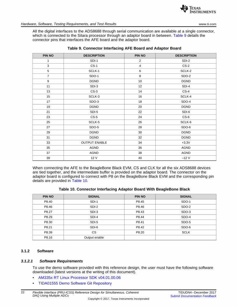
All the digital interfaces to the ADS8688 through serial communication are available at a single connector,which is connected to the Sitara processor through an adaptor board in between. Table 9 details theconnector pins that interfaces the AFE board and the adaptor board.
Table 9. Connector Interfacing AFE Board and Adaptor Board
PIN NO DESCRIPTION PIN NO DESCRIPTION1 SDI-1 2 SDI-23 CS-1 4 CS-25 SCLK-1 6 SCLK-27 SDO-1 8 SDO-29 DGND 10 DGND11 SDI-3 12 SDI-413 CS-3 14 CS-415 SCLK-3 16 SCLK-417 SDO-3 18 SDO-419 DGND 20 DGND21 SDI-5 22 SDI-623 CS-5 24 CS-625 SCLK-5 26 SCLK-627 SDO-5 28 SDO-629 DGND 30 DGND31 DGND 32 DGND33 OUTPUT ENABLE 34 +3.3V35 AGND 36 AGND37 AGND 38 AGND39 12 V 40 –12 V
When connecting the AFE to the BeagleBone Black EVM, CS and CLK for all the six ADS8688 devicesare tied together, and the intermediate buffer is provided on the adaptor board. The connector on theadaptor board is configured to connect with P8 on the BeagleBone Black EVM and the corresponding pindetails are provided in Table 10.
Table 10. Connector Interfacing Adaptor Board With BeagleBone Black
PIN NO SIGNAL PIN NO SIGNALP8.40 SDI-1 P8.45 SDO-1P8.46 SDI-2 P8.46 SDO-2P8.27 SDI-3 P8.43 SDO-3P8.29 SDI-4 P8.44 SDO-4P8.30 SDI-5 P8.41 SDO-5P8.21 SDI-6 P8.42 SDO-6P8.39 CS P8.20 SCLKP8.16 Output enable
3.1.2 Software
3.1.2.1 Software RequirementsTo use the demo software provided with this reference design, the user must have the following softwaredownloaded (latest versions at the writing of this document).• AM335x RT Linux Processor SDK v04.01.00.06• TIDA01555 Demo Software Git Repository
www.ti.com Hardware, Software, Testing Requirements, and Test Results
23TIDUDN4–December 2017Submit Documentation Feedback
Copyright © 2017, Texas Instruments Incorporated
Flexible Interface (PRU-ICSS) Reference Design for Simultaneous, CoherentDAQ Using Multiple ADCs
3.1.2.2 AM335x RT Linux Processor SDK InstallationThis reference design is written using a 64-bit version of an Ubuntu 14.04 LTS host machine.• Linux Processor SDK v04.01.00.06 download page: Processor SDK Download Page• Installation instructions: Processor SDK Linux Installer• Additional libraries if running a 64-bit distro: 64-bit Ubuntu Support• Processor SDK Linux Getting Started Guide
3.1.2.3 TIDA-01555 PRU ADC Demo SoftwareFind the demo software for this reference design in the TIDA-01555 git repository, and then clone thissoftware to the same Ubuntu development machine on which the RT Linux Processor SDK is installed.The repository can be cloned anywhere on the development machine; however, TI recommends to placethe package in the example-applications folder at the root of the RT Linux Processor v04.01.00.06installation.
3.1.2.4 Compile the Device Tree to Configure Pin MuxingA device tree file is provided in the dts folder of the TIDA-01555 git repository. Copy the device tree file(am335x-boneblack-pruadc.dts) into the dts folder of the RT Linux Kernel source of the Processor SDK.Find the dts folder at ${RT Linux Processor SDK Install Path}/board-support/linux-xx.xx.xx/arch/arm/boot/dts/.
After the am335x-boneblack-pruadc.dts file is placed in the SDK’s dts folder, compile the device tree.From the ${RT Linux Processor SDK Install Path}/board-support/linux-xx.xx.xx/ directory, run the followingbolded commands. Make sure to add the cross-compile toolchain to the PATH variable first. For moreinformation on the following commands, see the Processor SDK Linux Kernel Users Guide.• # make ARCH=arm CROSS_COMPILE=arm-linux-gnueabihf- distclean• # make ARCH=arm CROSS_COMPILE=arm-linux-gnueabihf- tisdk_am335x-evm-rt_defconfig• # make ARCH=arm CROSS_COMPILE=arm-linux-gnueabihf- am335x-boneblack-pruadc.dtb
3.1.2.5 Compiling the Arm User Space Binary and PRU-ICSS FirmwaresTo compile the Arm binary as well as the two PRU firmwares required to run the demo:1. Navigate to the top-level directory of the TIDA-01555 PRU ADC Demo Software Package on the host
machine (referred to as $ { PRU-ADC-DEMO-REPO }).2. A Makefile is provided for building both PRU-ICSS firmware images and the Arm user space binary.3. To successfully compile these binaries, the following environmental variables must be manually
exported (modify to reflect the correct path on the system).• Arm Cross-Compile Toolchain
Export ARM_CCT=${HOME}/ti-processor-sdk-linux-rt-am335x-evm-xx.xx.xx.xx/linux-devkit/sysroots/x86_64-arago-linux/usr/bin
• PRU Code Generation ToolsExport PRU_CGT=${HOME}/ti-processor-sdk-linux-rt-am335x-evm-xx.xx.xx.xx/linux-devkit/sysroots/x86_64-arago-linux/usr/share/ti/cgt-pru
• PRU Software Support PackageExport PRU_SSP=${HOME}/ti-processor-sdk-linux-rt-am335x-evm-xx.xx.xx.xx/example-applications/pru-icss-x.y.z
4. To build the binaries, navigate to the TIDA-01555 repository and execute the make command:• # cd ${PRU-ADC-DEMO-REPO}/• # make
NOTE: This top-level file Makefile calls Makefiles in each project folder, which can be called directlyto rebuild each binary separately.

Hardware, Software, Testing Requirements, and Test Results www.ti.com
24 TIDUDN4–December 2017Submit Documentation Feedback
Copyright © 2017, Texas Instruments Incorporated
Flexible Interface (PRU-ICSS) Reference Design for Simultaneous, CoherentDAQ Using Multiple ADCs
If nothing is missing, the binaries are located in the newly created gen folder inside each of the threeproject folders:• Arm user space application binary:
$ {PRU-ADC-DEMO-REPO}/ARM_User_Space_App/gen/Arm_User_Space_App.out• PRU-ICSS core 0 firmware binary:
${PRU-ADC-DEMO-REPO}/PRU_ADS8688_Controller/gen/PRU_ADS8688_Controller.out• PRU-ICSS core 1 firmware binary:
${PRU-ADC-DEMO-REPO}/PRU_ADS8688_Interface/gen/PRU_ADS8688_Interface.out
3.1.2.6 Copying Files to the File System of the BoardNow that all device trees, binaries, and firmwares have been built, move them over to the file system ofthe BeagleBone Black that is running the RT Linux Processor SDK Linux distribution.• Follow the Processor SDK Linux create SD card script wiki to create a bootable microSD card for the
BeagleBone Black EVM:– Create two partitions and install the pre-built images from the SDK when prompted.
• Put the newly created microSD card into the BeagleBone Black EVM.• Connect an Ethernet cable from the BeagleBone Black EVM to the same network that the
development machine is on.• Connect a USB-to-Serial cable between the BeagleBone Black EVM and development machine.• Open a serial console to see output messages from the BeagleBone Black (the example given uses
picocom and assumes the device is ttyUSB0). Type the following into the console of the developmentmachine:– # sudo picocom -b 115200 /dev/ttyUSB0
• Power up the BeagleBone Black and log in as user ‘root’ when the login prompt appears (there is nopassword).
• Find the IP address of the BeagleBone Black EVM using the ‘ifconfig’ utility. Type the following into theconsole of the BeagleBone Black:– # ifconfig
• Using the IP address found in the previous step, use an FTP client or SCP command line interface totransfer the following files to the following locations on the BeagleBone Black:– Copy the Arm user space binary that is built previously to the /home/root/ directory of the design
board’s file system:• ${PRU-ADC-DEMO-REPO}/ARM_User_Space_App/gen/Arm_User_Space_App.out
– Copy the two PRU-ICSS firmwares into the /lib/firmware/pru/ directory of the design board’s filesystem:• ${PRU-ADC-DEMO-REPO}/PRU_ADS8688_Controller/gen/PRU_ADS8688_Controller.out• ${PRU-ADC-DEMO-REPO}/PRU_ADS8688_Interface/gen/PRU_ADS8688_Interface.out
– Copy the device tree file into the /boot/ directory of the design board’s file system:• ${Proc SDK RT Linux Install Path}/arch/arm/boot/dts/am335x-boneblack-pruadc.dtb
• On the BeagleBone Black EVM, use the following commands to update the existing symbolic links inthe /lib/firmware/ directory of the design board’s file system to point to the new firmwares.– # cd /lib/firmware/– # rm am335x-pru0-fw; ln -s /lib/firmware/pru/PRU_ADS8688_Controller.out am335x-pru0-fw– # rm am335x-pru1-fw; ln -s /lib/firmware/pru/PRU_ADS8688_Interface.out am335x-pru1-fw
• Use the following commands to update the device tree file symbolic link in the /boot/ directory of thedesign board’s file system to point to the new device tree:– # cd /boot/– # rm am335x-boneblack.dtb; ln -s am335x-boneblack-pruadc.dtb am335x-boneblack.dtb

www.ti.com Hardware, Software, Testing Requirements, and Test Results
25TIDUDN4–December 2017Submit Documentation Feedback
Copyright © 2017, Texas Instruments Incorporated
Flexible Interface (PRU-ICSS) Reference Design for Simultaneous, CoherentDAQ Using Multiple ADCs
3.1.2.7 Booting and Running the DemoWith everything in place, reboot the design board for the new device tree file to take effect. Keepeverything plugged into the BeagleBone Black (the USB-to-Serial cable, the network cable, the powercable, and so on) and either use the reboot command on the board’s console or the reset button next tothe Ethernet jack to reboot the board. Now that the board is rebooted and everything is in place, run thedemo.• Start the PRU cores using their sysfs interface:
– # echo ‘start’ > /sys/class/remoteproc/remoteproc1/state– # echo ‘start’ > /sys/class/remoteproc/remoteproc2/state
• Run the Arm user space program to start the demo:– # cd /home/root/– # ./ARM_User_Space_App.out
The minimum, maximum, and RMS values for each ADC channel then appear on the BeagleBone Black’sconsole coming from the user space application. Press any button to end the demo and return to theconsole.
If the data received on the console does not match expectations, use a logic analyzer to ensure that thePRU’s pins are in fact toggling to implement the SPI. If there is no activity on the pins, double check thesteps in Section 3.1.2.4 to affect the pin mux of the device and determine whether or not the PRU coresare able to toggle pins.
The PRUs are free running in this demo; once started, the PRUs continue to collect ADC data and place itinto the ping and pong buffers in the DDR until they are stopped. To stop them, use their sysfs interface:• # echo ‘stop’ > /sys/class/remoteproc/remoteproc1/state• # echo ‘stop’ > /sys/class/remoteproc/remoteproc2/state
Stopping the PRUs, replacing their /lib/firmware/am335x-pruN-fw file, and then restarting them is themethod used to swap out the PRU’s firmware.
3.1.2.8 Software DisclaimerThe software provided is proven to build and run correctly on the 4.1.0.6 version of the RT LinuxProcessor SDK. Using a different version of the SDK or different hardware components has not beentested and must be verified by the user.
Copyright © 2017, Texas Instruments Incorporated
±10-V function generator
Analog signal conditioning
interface
SDO
CS
SDI
SCLK
ADS8688EVMSDCC interface
ADS8688EVMGUI
Voltage supply
5.5 V
Hardware, Software, Testing Requirements, and Test Results www.ti.com
26 TIDUDN4–December 2017Submit Documentation Feedback
Copyright © 2017, Texas Instruments Incorporated
Flexible Interface (PRU-ICSS) Reference Design for Simultaneous, CoherentDAQ Using Multiple ADCs
3.2 Testing and Results
3.2.1 Functional Tests• Power tree: Before testing for performance, the data acquisition board is powered up by giving the 5.5-
V supply at the input. Voltage at different test points are measured to validate the ±12 V, +5 V and+3.3 V rails.
• Analog driver: Using a function generator, AFE of the board is tested by giving AC voltage of less thana ±10-V peak at the analog input pins. This is to verify voltages going at the input of ADS8688 andfunctioning of analog driver for the same.
• Sensor board: Functioning of the sensor board is verified by connecting CTs and PTs at thecorresponding connectors. Voltage at the input of PT is swung up to 120-V AC RMS to make sureoutput of the sensor board is within the input voltage range of ±10.24 V. Similarly, on the CT, inputcurrent is given up to 70 A RMS to validate the output of the board is limited within the range of theADC.
• ADS8688: To verify how the AFE and ADS8688 boards function, the test setup shown in Figure 21 isused where the ADS8688EVM along with a simple capture card (SDCC) evaluate the performance ofan individual ADC.– DC performance: By shorting the input signal connector on the AFE board, DC performance of the
ADC is captured using the graphical user interface (GUI) through a USB interface. The histogramanalysis provides a mean ADC value, code spread, sigma (standard deviation), and the peak valuefor zero input.
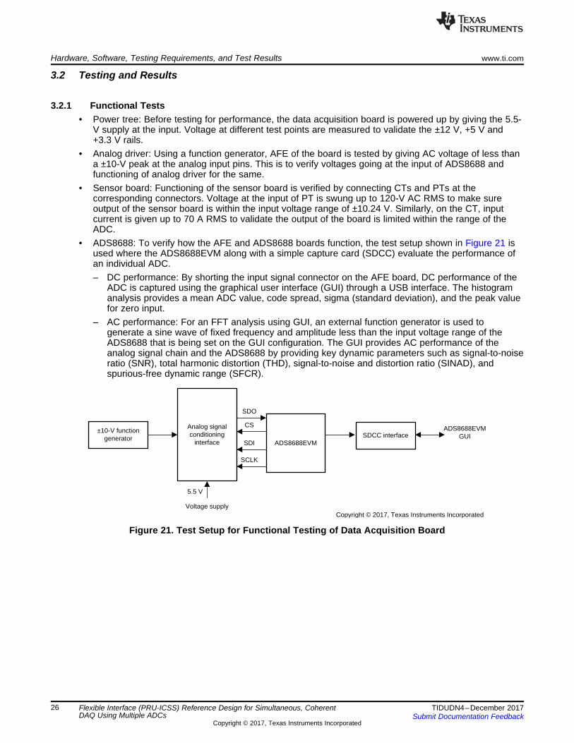
– AC performance: For an FFT analysis using GUI, an external function generator is used togenerate a sine wave of fixed frequency and amplitude less than the input voltage range of theADS8688 that is being set on the GUI configuration. The GUI provides AC performance of theanalog signal chain and the ADS8688 by providing key dynamic parameters such as signal-to-noiseratio (SNR), total harmonic distortion (THD), signal-to-noise and distortion ratio (SINAD), andspurious-free dynamic range (SFCR).
Figure 21. Test Setup for Functional Testing of Data Acquisition Board
Sensor board
Adapter card
Analog signal conditioning
interface
Voltage supply
5.5 V
CTs
PTs
Voltage and current source BeagleBone Black
www.ti.com Hardware, Software, Testing Requirements, and Test Results
27TIDUDN4–December 2017Submit Documentation Feedback
Copyright © 2017, Texas Instruments Incorporated
Flexible Interface (PRU-ICSS) Reference Design for Simultaneous, CoherentDAQ Using Multiple ADCs
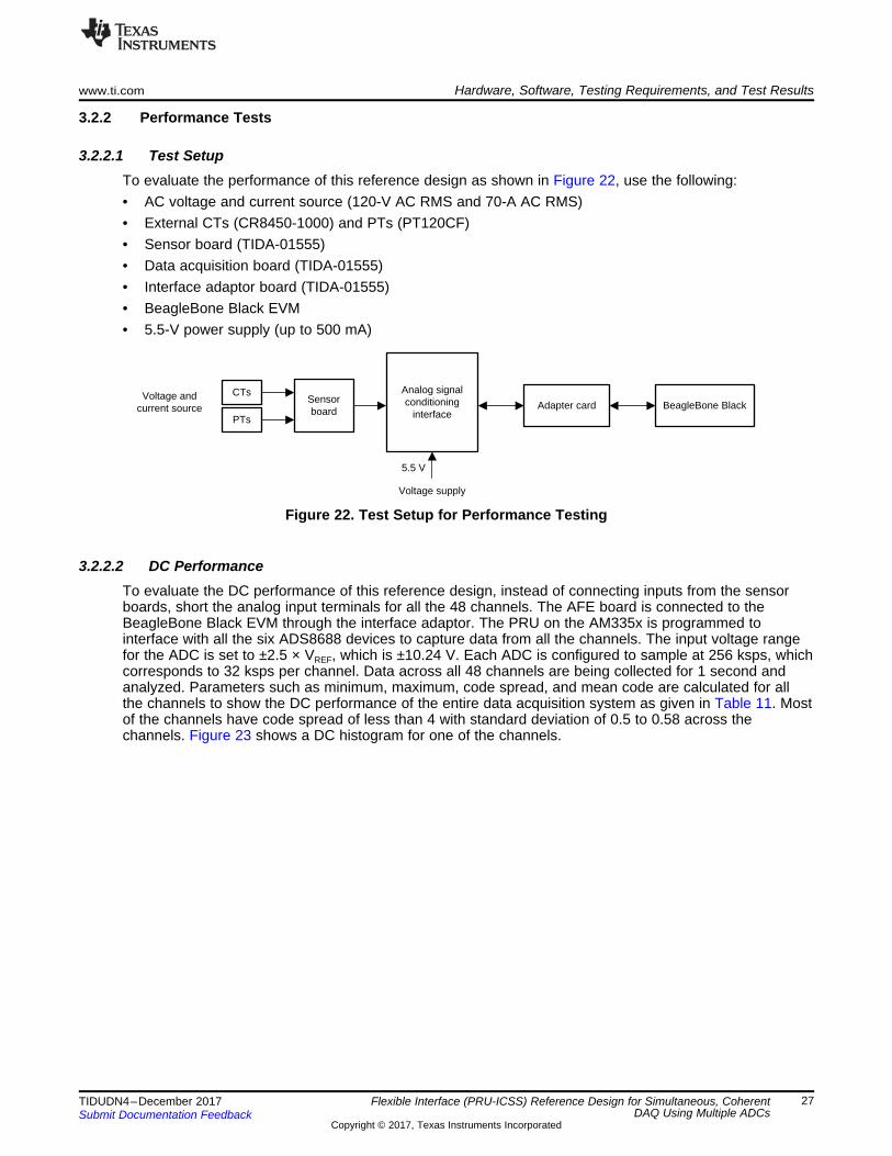
3.2.2 Performance Tests
3.2.2.1 Test SetupTo evaluate the performance of this reference design as shown in Figure 22, use the following:• AC voltage and current source (120-V AC RMS and 70-A AC RMS)• External CTs (CR8450-1000) and PTs (PT120CF)• Sensor board (TIDA-01555)• Data acquisition board (TIDA-01555)• Interface adaptor board (TIDA-01555)• BeagleBone Black EVM• 5.5-V power supply (up to 500 mA)
Figure 22. Test Setup for Performance Testing
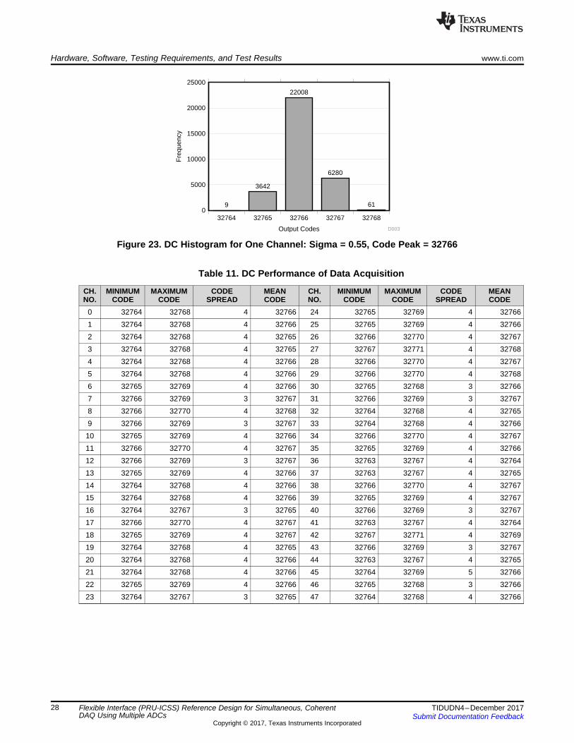
3.2.2.2 DC PerformanceTo evaluate the DC performance of this reference design, instead of connecting inputs from the sensorboards, short the analog input terminals for all the 48 channels. The AFE board is connected to theBeagleBone Black EVM through the interface adaptor. The PRU on the AM335x is programmed tointerface with all the six ADS8688 devices to capture data from all the channels. The input voltage rangefor the ADC is set to ±2.5 × VREF, which is ±10.24 V. Each ADC is configured to sample at 256 ksps, whichcorresponds to 32 ksps per channel. Data across all 48 channels are being collected for 1 second andanalyzed. Parameters such as minimum, maximum, code spread, and mean code are calculated for allthe channels to show the DC performance of the entire data acquisition system as given in Table 11. Mostof the channels have code spread of less than 4 with standard deviation of 0.5 to 0.58 across thechannels. Figure 23 shows a DC histogram for one of the channels.
Output Codes
Fre
quen
cy
0
5000
10000
15000
20000
25000
32764 32765 32766 32767 32768
9
3642
22008
6280
61
D003
Hardware, Software, Testing Requirements, and Test Results www.ti.com
28 TIDUDN4–December 2017Submit Documentation Feedback
Copyright © 2017, Texas Instruments Incorporated
Flexible Interface (PRU-ICSS) Reference Design for Simultaneous, CoherentDAQ Using Multiple ADCs
Figure 23. DC Histogram for One Channel: Sigma = 0.55, Code Peak = 32766
Table 11. DC Performance of Data Acquisition
CH.NO.
MINIMUMCODE
MAXIMUMCODE
CODESPREAD
MEANCODE
CH.NO.
MINIMUMCODE
MAXIMUMCODE
CODESPREAD
MEANCODE
0 32764 32768 4 32766 24 32765 32769 4 327661 32764 32768 4 32766 25 32765 32769 4 327662 32764 32768 4 32765 26 32766 32770 4 327673 32764 32768 4 32765 27 32767 32771 4 327684 32764 32768 4 32766 28 32766 32770 4 327675 32764 32768 4 32766 29 32766 32770 4 327686 32765 32769 4 32766 30 32765 32768 3 327667 32766 32769 3 32767 31 32766 32769 3 327678 32766 32770 4 32768 32 32764 32768 4 327659 32766 32769 3 32767 33 32764 32768 4 32766
10 32765 32769 4 32766 34 32766 32770 4 3276711 32766 32770 4 32767 35 32765 32769 4 3276612 32766 32769 3 32767 36 32763 32767 4 3276413 32765 32769 4 32766 37 32763 32767 4 3276514 32764 32768 4 32766 38 32766 32770 4 3276715 32764 32768 4 32766 39 32765 32769 4 3276716 32764 32767 3 32765 40 32766 32769 3 3276717 32766 32770 4 32767 41 32763 32767 4 3276418 32765 32769 4 32767 42 32767 32771 4 3276919 32764 32768 4 32765 43 32766 32769 3 3276720 32764 32768 4 32766 44 32763 32767 4 3276521 32764 32768 4 32766 45 32764 32769 5 3276622 32765 32769 4 32766 46 32765 32768 3 3276623 32764 32767 3 32765 47 32764 32768 4 32766

AC Votage in RMS
Y A
xis
Titl
e (U
nit)
0 20 40 60 80 100 120 140-0.14
-0.12
-0.1
-0.08
-0.06
-0.04
-0.02
0
0.02
0.04
0.06
D001
www.ti.com Hardware, Software, Testing Requirements, and Test Results
29TIDUDN4–December 2017Submit Documentation Feedback
Copyright © 2017, Texas Instruments Incorporated
Flexible Interface (PRU-ICSS) Reference Design for Simultaneous, CoherentDAQ Using Multiple ADCs
3.2.2.3 AC PerformanceTo test the board for accuracy of AC signals, a variable voltage and current source are connected at theinput of the PTs and CTs. Figure 22 shows the setup used to sweep the input voltage and current signals.The frequency of the input voltage and current is set to 50 Hz. For every line cycle, 640 samples arecollected for each channel through SPI. The ping-pong buffer stores the data corresponding to one cyclefrom all the 48 channels. RMS value is being calculated for using this data for every cycle and stored in abuffer. Input AC voltage is varied from 2.5-V to 120-V RMS and the measurement accuracy has beencaptured in Figure 24 and Table 12. This error includes total error of the system including non-linearity ofthe PTs.
Figure 24. Performance of DAQ for AC Voltage Measurement
Table 12. Accuracy of AC Voltage Measurement
VOLTAGE(VRMS)
APPLIED VOLTAGE(VRMS)
MEASURED VOLTAGEAT ADC (VRMS)
MEASURED VOLTAGEAFTER CALIBRATION (VRMS) % ERROR
2.5 2.477 0.1028 2.4771 –0.00445 5.002 0.2075 5.0000 0.0400
10 10.002 0.4152 10.0048 –0.028220 20.0016 0.8303 20.0072 –0.028130 30.002 1.2454 30.0096 –0.025540 40.0022 1.6605 40.0120 –0.024650 50.0025 2.076 50.0241 –0.043275 75.003 3.1159 75.0819 –0.1052
100 100.003 4.155 100.1205 –0.1175110 110.004 4.5706 110.1349 –0.1190120 120.005 4.9849 120.1181 –0.0942
AC Current in RMS
% E
rror
0 10 20 30 40 50 60 70-0.1
-0.06
-0.02
0.02
0.06
0.1
0.14
0.18
D002
Hardware, Software, Testing Requirements, and Test Results www.ti.com
30 TIDUDN4–December 2017Submit Documentation Feedback
Copyright © 2017, Texas Instruments Incorporated
Flexible Interface (PRU-ICSS) Reference Design for Simultaneous, CoherentDAQ Using Multiple ADCs
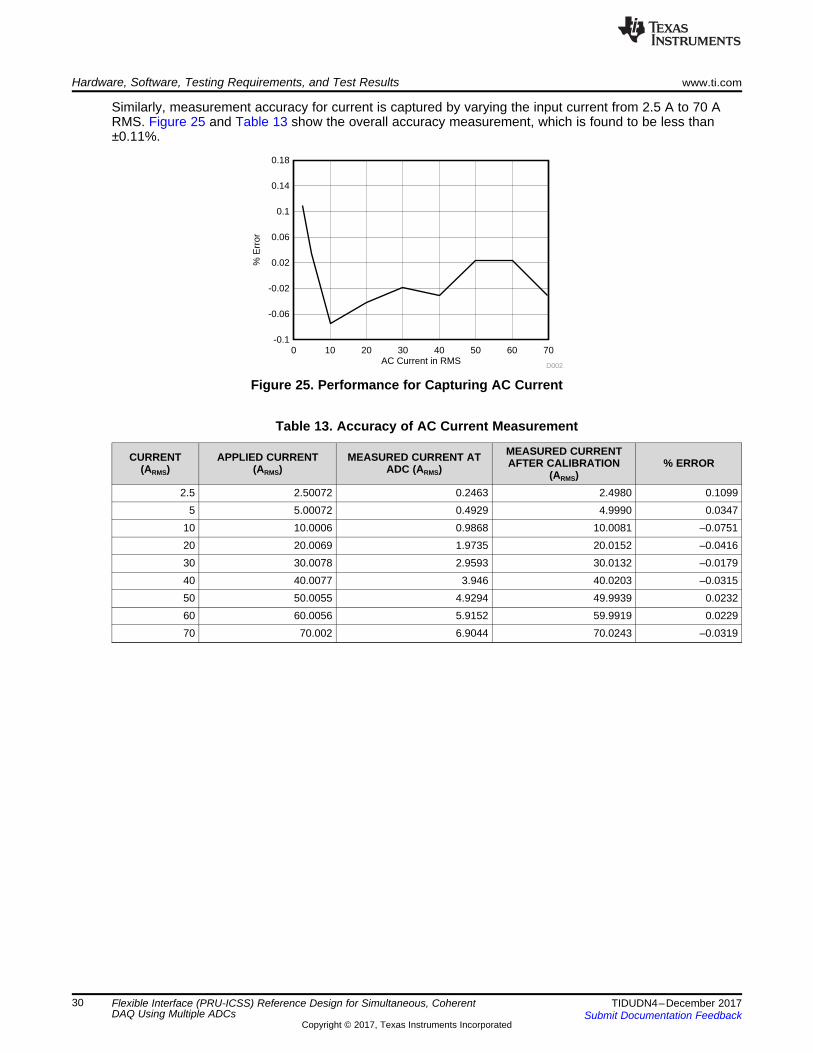
Similarly, measurement accuracy for current is captured by varying the input current from 2.5 A to 70 ARMS. Figure 25 and Table 13 show the overall accuracy measurement, which is found to be less than±0.11%.
Figure 25. Performance for Capturing AC Current
Table 13. Accuracy of AC Current Measurement
CURRENT(ARMS)
APPLIED CURRENT(ARMS)
MEASURED CURRENT ATADC (ARMS)
MEASURED CURRENTAFTER CALIBRATION
(ARMS)% ERROR
2.5 2.50072 0.2463 2.4980 0.10995 5.00072 0.4929 4.9990 0.0347
10 10.0006 0.9868 10.0081 –0.075120 20.0069 1.9735 20.0152 –0.041630 30.0078 2.9593 30.0132 –0.017940 40.0077 3.946 40.0203 –0.031550 50.0055 4.9294 49.9939 0.023260 60.0056 5.9152 59.9919 0.022970 70.002 6.9044 70.0243 –0.0319

www.ti.com Hardware, Software, Testing Requirements, and Test Results
31TIDUDN4–December 2017Submit Documentation Feedback
Copyright © 2017, Texas Instruments Incorporated
Flexible Interface (PRU-ICSS) Reference Design for Simultaneous, CoherentDAQ Using Multiple ADCs
3.2.2.4 Simultaneous Sampling Between ADCsIn this design, all the six ADCs have a common CS signal. Sampling delay between nth channel of all theADCs will be minimal. For example, CH0 of ADC1, CH0 of ADC2, and CH0 of ADC6 must have a verysmall delay between sampling. This delay is verified by performing the following test:• Configure all the ADCs to sample only first channel of its input (that is, CH0). This results in higher
throughput and smaller conversion time.• Apply an input signal of 50 Hz to CH0 of all the ADCs.• Configure the ADCs to capture at full speed of 256 ksps for each ADS8688.• Capture the data from each ADC for 1 second, which results in 256k samples for each input channel.• Compare the ADC sample number corresponding to maximum value and minimum value in two ADCs.
Table 14 shows the output value from two ADCs near the minimum and maximum values captured alongwith the sample number. From both of these values, there is a delay of one sample and half sample cyclein these two cases. From the experiment, the maximum delay between two channels is no more than 1sample cycle, which is 3.9 µs.
Table 14. Sample Numbers Around Peak Values for Two ADCs
SAMPLENUMBER
OUTPUT FROM CH-0OF ADC-1
OUTPUT FROM CH-0OF ADC-2
SAMPLENUMBER
OUTPUT FROM CH-0 OFADC-1
OUTPUT FROM CH-0 OF ADC-2
525 1893 1897 3087 63595 63593526 1893 1897 3088 63596 63593527 1893 1896 3089 63596 63594528 1892 1896 3090 63596 63594529 1892 1896 3091 63596 63594530 1892 1895 3092 63595 63593531 1893 1896 3093 63594 63592
3.2.2.5 Coherent SamplingIn this reference design, input frequency is estimated by detecting zero crossing of the input signal. Thisdetection is implemented on the second PRU core, which counts the number of zero crossings of thesignal captured at a user specified channel. In this example, the core captures time taken for 10 zerocrossings, which corresponds to five line cycles. Based on this computation, the PCU can update thesampling rate of acquisition on the first PRU to precisely adjust the CS to achieve fixed number ofsamples in spite of variations in the line cycle.
To validate the functioning of coherent sampling, logic analyzer is plugged on to the CS pin and voltage isfed from a function generator to the corresponding channel, which is programmed to detect frequency andzero crossing. Initially, the input signal is set to 50 Hz, which results in an overall conversion time of 3.91µs, or 255.8 kHz (50 Hz × 640 samples × 8 channels). When the input signal frequency is changed to 45Hz, the frequency of the CS signal also changes accordingly to 4.34 µs, or 230.4 kHz (45 Hz × 640samples × 8 channels). Figure 26 shows the transition between two situations.
Figure 26. Adjusting CS for Coherent Sampling
Hardware, Software, Testing Requirements, and Test Results www.ti.com
32 TIDUDN4–December 2017Submit Documentation Feedback
Copyright © 2017, Texas Instruments Incorporated
Flexible Interface (PRU-ICSS) Reference Design for Simultaneous, CoherentDAQ Using Multiple ADCs
Figure 27 demonstrates the improvement in the AC performance of data acquisition due to coherentsampling. In the initial setup, coherent sampling is disabled and the sampling rate is fixed to 256 ksps,which results in 640 samples per cycle when the input frequency is 50 Hz. A sampling window of 1280samples is used to analyze FFT. In this analysis, an input voltage of 45 Hz is given to one of the analogchannels and the data is being captured. Time samples of the ADC output is plotted on the left side andFFT plot on the right-hand side of Figure 27.
When the coherent sampling is disabled, fewer than two cycles are captured on the given samplingwindow as shown in the right-top plot, and the corresponding FFT plot is shown next to it. With thecoherent sampling enabled, PRU can able estimate the input frequency by looking at the zero crossings.This adjusts the CS to achieve a fixed 640 samples per cycle in spite of any variations in the inputfrequency, which is evident in the bottom plot of Figure 27. Exactly two cycles are captured in a samplingwindow of 1280 samples, which results in an improved FFT plot with reduced spectral leakage.
Figure 27. Comparison of AC Performance for Non-Coherent and Coherent Sampling
www.ti.com Hardware, Software, Testing Requirements, and Test Results
33TIDUDN4–December 2017Submit Documentation Feedback
Copyright © 2017, Texas Instruments Incorporated
Flexible Interface (PRU-ICSS) Reference Design for Simultaneous, CoherentDAQ Using Multiple ADCs
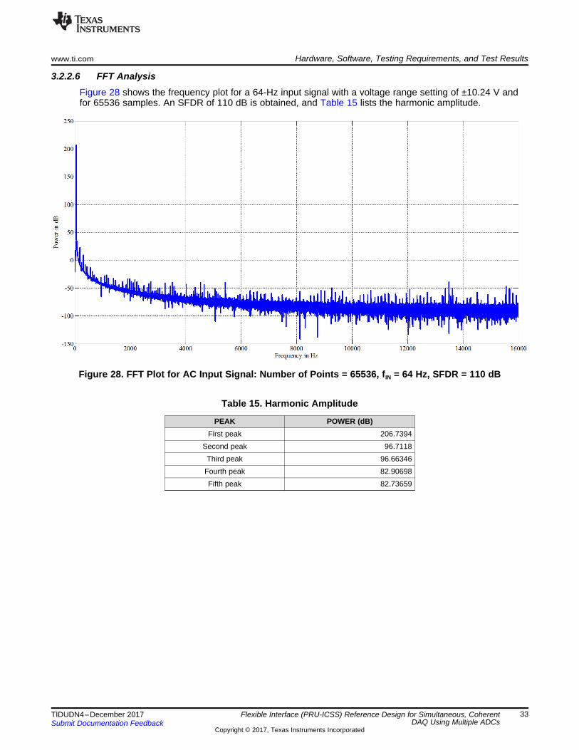
3.2.2.6 FFT AnalysisFigure 28 shows the frequency plot for a 64-Hz input signal with a voltage range setting of ±10.24 V andfor 65536 samples. An SFDR of 110 dB is obtained, and Table 15 lists the harmonic amplitude.
Figure 28. FFT Plot for AC Input Signal: Number of Points = 65536, fIN = 64 Hz, SFDR = 110 dB
Table 15. Harmonic Amplitude
PEAK POWER (dB)First peak 206.7394
Second peak 96.7118Third peak 96.66346
Fourth peak 82.90698Fifth peak 82.73659
Design Files www.ti.com
34 TIDUDN4–December 2017Submit Documentation Feedback
Copyright © 2017, Texas Instruments Incorporated
Flexible Interface (PRU-ICSS) Reference Design for Simultaneous, CoherentDAQ Using Multiple ADCs
4 Design Files
4.1 SchematicsTo download the schematics, see the design files at TIDA-01555.
4.2 Bill of MaterialsTo download the bill of materials (BOM), see the design files at TIDA-01555.
4.3 PCB Layout RecommendationsPerformance of data acquisition is highly dependent on the design and layout of PCB in both analog anddigital sides. Addressing the details of PCB design is critical to ensure the best performance out of theADC. For more details, see ADS868x 16-Bit, 500-kSPS, 4- and 8-Channel, Single-Supply, SAR ADCs withBipolar Input Ranges.
4.3.1 Layout PrintsTo download the layer plots, see the design files at TIDA-01555.
4.4 Altium ProjectTo download the Altium project files, see the design files at TIDA-01555.
4.5 Gerber FilesTo download the Gerber files, see the design files at TIDA-01555.
4.6 Assembly DrawingsTo download the assembly drawings, see the design files at TIDA-01555.
5 Software FilesTo download the software files for this reference design, see the link at TIDA-01555.
6 Related Documentation1. Texas Instruments, TIDA-00307 High-Accuracy AC Voltage and Current Measurement AFE for Feeder
Terminal Unit Reference Design2. Texas Instruments, ADS8688EVM-PDK Evaluation Module User's Guide3. Texas Instruments, TIDA-01214 Isolated, High-Accuracy Analog Input Module Reference Design Using
16-Bit ADC and Digital Isolator
6.1 TrademarksSitara, E2E are trademarks of Texas Instruments.Arm, Cortex are registered trademarks of Arm Limited (or its subsidiaries).All other trademarks are the property of their respective owners.
www.ti.com Terminology
35TIDUDN4–December 2017Submit Documentation Feedback
Copyright © 2017, Texas Instruments Incorporated
Flexible Interface (PRU-ICSS) Reference Design for Simultaneous, CoherentDAQ Using Multiple ADCs
7 TerminologyADC— Analog-to-digital converter
AFE— Analog front end
CT— Current transformer
FFT— Fast Fourier transform
GUI— Graphic user interface
LPF— Low-pass filter
PRU— Programmable real-time unit
PT— Potential transformer
SFDR— Spurious-free dynamic range
SINAD— Signal-to-noise and distortion ratio
SNR— Signal-to-noise ratio
THD— Total harmonic distortion
8 About the AuthorsPRASANNA RAJAGOPAL is a systems engineer at Texas Instruments Dallas, where he is responsiblefor developing reference design solutions for Grid Infrastructure in Industrial Systems. Prasanna brings tothis role his expertise in power electronics, mixed signal systems. Prasanna earned his PhD from IISc,Bangalore, India.
JASON REEDER is a software applications engineer at Texas Instruments, where he is responsible forsupporting customers using Linux on TI’s Sitara family of devices. Jason earned his bachelor of science incomputer software engineering and his master of science in electrical engineering at the University ofFlorida in Gainesville, FL.
8.1 AcknowledgmentsKALLIKUPPA MUNIYAPPA SREENIVASA, Systems Architect at Texas Instruments, for his inputs andfeedback on system architecture, requirements, and technical inputs.
AMIT KUMBASI, Systems Manager at Texas Instruments, for his inputs and feedback on systemarchitecture, requirements, and technical inputs.

IMPORTANT NOTICE FOR TI DESIGN INFORMATION AND RESOURCES
Texas Instruments Incorporated (‘TI”) technical, application or other design advice, services or information, including, but not limited to,reference designs and materials relating to evaluation modules, (collectively, “TI Resources”) are intended to assist designers who aredeveloping applications that incorporate TI products; by downloading, accessing or using any particular TI Resource in any way, you(individually or, if you are acting on behalf of a company, your company) agree to use it solely for this purpose and subject to the terms ofthis Notice.TI’s provision of TI Resources does not expand or otherwise alter TI’s applicable published warranties or warranty disclaimers for TIproducts, and no additional obligations or liabilities arise from TI providing such TI Resources. TI reserves the right to make corrections,enhancements, improvements and other changes to its TI Resources.You understand and agree that you remain responsible for using your independent analysis, evaluation and judgment in designing yourapplications and that you have full and exclusive responsibility to assure the safety of your applications and compliance of your applications(and of all TI products used in or for your applications) with all applicable regulations, laws and other applicable requirements. Yourepresent that, with respect to your applications, you have all the necessary expertise to create and implement safeguards that (1)anticipate dangerous consequences of failures, (2) monitor failures and their consequences, and (3) lessen the likelihood of failures thatmight cause harm and take appropriate actions. You agree that prior to using or distributing any applications that include TI products, youwill thoroughly test such applications and the functionality of such TI products as used in such applications. TI has not conducted anytesting other than that specifically described in the published documentation for a particular TI Resource.You are authorized to use, copy and modify any individual TI Resource only in connection with the development of applications that includethe TI product(s) identified in such TI Resource. NO OTHER LICENSE, EXPRESS OR IMPLIED, BY ESTOPPEL OR OTHERWISE TOANY OTHER TI INTELLECTUAL PROPERTY RIGHT, AND NO LICENSE TO ANY TECHNOLOGY OR INTELLECTUAL PROPERTYRIGHT OF TI OR ANY THIRD PARTY IS GRANTED HEREIN, including but not limited to any patent right, copyright, mask work right, orother intellectual property right relating to any combination, machine, or process in which TI products or services are used. Informationregarding or referencing third-party products or services does not constitute a license to use such products or services, or a warranty orendorsement thereof. Use of TI Resources may require a license from a third party under the patents or other intellectual property of thethird party, or a license from TI under the patents or other intellectual property of TI.TI RESOURCES ARE PROVIDED “AS IS” AND WITH ALL FAULTS. TI DISCLAIMS ALL OTHER WARRANTIES ORREPRESENTATIONS, EXPRESS OR IMPLIED, REGARDING TI RESOURCES OR USE THEREOF, INCLUDING BUT NOT LIMITED TOACCURACY OR COMPLETENESS, TITLE, ANY EPIDEMIC FAILURE WARRANTY AND ANY IMPLIED WARRANTIES OFMERCHANTABILITY, FITNESS FOR A PARTICULAR PURPOSE, AND NON-INFRINGEMENT OF ANY THIRD PARTY INTELLECTUALPROPERTY RIGHTS.TI SHALL NOT BE LIABLE FOR AND SHALL NOT DEFEND OR INDEMNIFY YOU AGAINST ANY CLAIM, INCLUDING BUT NOTLIMITED TO ANY INFRINGEMENT CLAIM THAT RELATES TO OR IS BASED ON ANY COMBINATION OF PRODUCTS EVEN IFDESCRIBED IN TI RESOURCES OR OTHERWISE. IN NO EVENT SHALL TI BE LIABLE FOR ANY ACTUAL, DIRECT, SPECIAL,COLLATERAL, INDIRECT, PUNITIVE, INCIDENTAL, CONSEQUENTIAL OR EXEMPLARY DAMAGES IN CONNECTION WITH ORARISING OUT OF TI RESOURCES OR USE THEREOF, AND REGARDLESS OF WHETHER TI HAS BEEN ADVISED OF THEPOSSIBILITY OF SUCH DAMAGES.You agree to fully indemnify TI and its representatives against any damages, costs, losses, and/or liabilities arising out of your non-compliance with the terms and provisions of this Notice.This Notice applies to TI Resources. Additional terms apply to the use and purchase of certain types of materials, TI products and services.These include; without limitation, TI’s standard terms for semiconductor products http://www.ti.com/sc/docs/stdterms.htm), evaluationmodules, and samples (http://www.ti.com/sc/docs/sampterms.htm).
Mailing Address: Texas Instruments, Post Office Box 655303, Dallas, Texas 75265Copyright © 2017, Texas Instruments Incorporated
Recommended