Computational Electronics Group
2002 School on Computational Material Science May 21-31, 2002
Full Band Monte Carlo Simulation
Umberto Ravaioli
Beckman Institute andDepartment of Electrical and Computer Engineering
University of Illinois at Urbana-ChampaignUrbana, IL 61801, USA
University of Illinois

2002 School on Computational Material Science May 21-31, 2002
• The conduction (valence) band is represented by a parabolicdispersion relation, only close to the energy minima.
• Non-parabolicity may extend analytical representations of thebands but may also have limited validity. In silicon, forinstance, typically above 1.0 eV, the density of states in theconduction band may not be approximated by a non-parabolicdispersion relation.
• Valence bands may have strong warping, which is difficult torepresent analytically.
• At higher energies there may be satellite minima and otherband braches start to appear.
Issues

• Textbook picture of band structureSilicon band structure
2002 School on Computational Material Science May 21-31, 2002

• Contour plots
First band Second band
Silicon band structure
2002 School on Computational Material Science May 21-31, 2002

• 3D isosurfaces - Video animationSilicon band structure
2002 School on Computational Material Science May 21-31, 2002

• First conduction band near minimumSilicon band structure
2002 School on Computational Material Science May 21-31, 2002
Full band
non-parabolic

Silicon density of states
2002 School on Computational Material Science May 21-31, 2002

• The band structure of semiconductors may be obtained byusing a variety of methods, known as tight-binding, k · p, localand non-local pseudopotentials, etc.
• For semiconductor bandstructure, we find it useful to adoptpseudopotential methods. We review in the following thesteps to solve a bandstructure problem with the localempirical pseudopotential approach.
• The pseudopotential method assume a “reasonable form” ofthe potential due to the atom from nucleus up to coreelectrons. The states for valence electrons are solved, and asoutcome of the program we obtain the eigenvaluescorresponding to valence and conduction bands.
Band structure calculations
2002 School on Computational Material Science May 21-31, 2002

• Our goal is to solve the Schrödinger equation
to obtain the allowed values of energy E for a given value of kfor the valence electrons.
• From Block’s theorem
Empirical pseudopotentials
2002 School on Computational Material Science May 21-31, 2002
22
0( ) ( ) ( ) ( )
2r V r r E r
mψ ψ ψ− ∇ + =
( ) ( )( )
ˆ,
( ) and are periodic with the lattice
j k rk
k
k r e u r
V r u r
ψ ⋅=

• We can expand in terms of reciprocal lattice vectors andsubstitute in Schrödinger equation
Empirical pseudopotentials
2002 School on Computational Material Science May 21-31, 2002
( )
( )
ˆ
ˆ
2 ˆ2 ( )
0ˆ ˆ( ) ( )
2
( )
hh
mm
hh
h m hm h
j K rk K
hj K r
Km
j k K rh K
hj k K K r j k K r
K Km h h
u r A e
V r V e
k K A em
V e E k A e
⋅
⋅
+ ⋅
+ + ⋅ + ⋅
=
=
⇒ +
+ =
∑
∑
∑
∑∑ ∑

• Now multiply by
and integrate over the volume of the crystal (Fouriertransform), with result
Empirical pseudopotentials
2002 School on Computational Material Science May 21-31, 2002
ˆ ( ) 0, 1, ,lj k K re l n− + ⋅ = …
( )2 2
0( )
2 h l h h llK K K K Kh
A k K V A E k Am −+ + =∑

• In matrix form
• For a given wave vector k, we can determine the bandstructure values E(k) by solving this eigenvalue solver.
Empirical pseudopotentials
2002 School on Computational Material Science May 21-31, 2002
( )
0 0
1 1
2 2
0,0 0,1 0,2 0,
1,0 1,1 1,2 1,
2,0 2,1 2,2 2,
,0 ,1 ,2 ,
22
02
n n
i j
K Kn
K Kn
n K K
n n n n n K K
iij
K K
A Aa a a aA Aa a a a
a a a a E KA A
a a a a A A
k K i jma
V i j−
=
+ ==
≠

• Technical issue: how big should n be? Band structureexperts indicate that n ≈ 120 should give satisfactory results.
• The coefficients expressing the potential can be decomposedinto a symmetric and an antisymmetric part
Empirical pseudopotentials
2002 School on Computational Material Science May 21-31, 2002
( )
( ) ( )structure structurepseudopotential pseudopotential
factor factorform factor form factor
ˆ
symmetric antisymmetric
ˆ
mm
m m m
j K rK
m
s s a am mK K K
V r V e
V S K F j S K F
⋅=
= +
∑

Empirical pseudopotentials
2002 School on Computational Material Science May 21-31, 2002
( ) ( ) ( ) ( )( ) ( ) ( ) ( )
( ) ( )
( ) ( )
1 2 1 2
ˆ 31 1
ˆ 32 2
cos ; sin
;2 2
2
2
m m
m
m
s am m m m
m m m ms aK K
j K rm
j K rm
S K K S K K
V K V K V K V KF F
V K V r e d r
V K V r e d r
τ τ
Ω
Ω
− ⋅
− ⋅
= ⋅ = ⋅
+ −= =
=
=
∫
∫
The diamond and zinc-blende type semiconductor have fccstructure with 2 atoms per cell. The origin is taken halfwaybetween these two atoms with position
and1 2(1 8,1 8,1 8) ; ( 1 8, 1 8, 1 8)r r= = − − −

Empirical pseudopotentials
2002 School on Computational Material Science May 21-31, 2002
and are the pseudopotentials due to singleatoms in the lattice and Ω is the volume of the unit cell.
For diamond structure
The first five of the reciprocal lattice vectors for fcc structurehave squared magnitude of 0,3,4,8,11 in the units of (2π/a)2.
Only these vectors are allowed to have a non-zero potential.
( )1V r ( )2V r
( ) ( )1 2
0m
m
sm mK
aK
V V K V K
V
= =
=

Empirical pseudopotentials
2002 School on Computational Material Science May 21-31, 2002
Form factors are taken in a local and static approximation, to beindependent of momentum and energy, so that they canproduce average potentials for the whole Brillouin zone and theentire range of energy of the valence and conduction bands.
Below is a table of form factors for Si and Ga. The localpseudopotential approximation is better for Si. For a polarmaterial like GaAs, anti-symmetric form factors are to beconsidered, leading to a complex eigenvalue problem. Somedetails of the bandstructure are more accurately reproduced if amore complicated non-local approach is taken for GaAs.
3 4 8 11 3 4 8 110.224 0.0 0.055 0.072 0.0 0.0 0.0 0.0 5.4310.23 0.0 0.01 0.06 0.07 0.12 0.07 0.02 5.65
s s s s a a a aElement F F F F F F F F a
SiGaAs
−−

Empirical pseudopotentials
2002 School on Computational Material Science May 21-31, 2002
The computational cost of band structure calculations can besignificantly reduced if the symmetry of the Brillouin zone isexploited. Only 1/48 (irreducible wedge) of the fcc Brillouin zoneis necessary. The irreducible wedge is determined by thefollowing equations (wave vectors normalized with 2π/a)
0 1
32
z x y
x y z
k k k
k k k
∗ ∗ ∗
∗ ∗ ∗
≤ ≤ ≤ ≤
+ + ≤

Bulk Monte Carlo simulation of Silicon
Effect of band structure on high-field transport
2002 School on Computational Material Science May 21-31, 2002

Full band Monte Carlo implementations
Complete model:
k-dependent scattering ratesRequires storage of very large scattering rate tablesTake fully into account material anisotropySuitable for material parameter calculations
Simplified model:
Energy-dependent scattering ratesSame storage requirements as conventional MCNeglects anisotropy of scatteringSuitable for device simulation
2002 School on Computational Material Science May 21-31, 2002
Two main objections can be raised against full bandstructure approaches:
(i) Details of the band structure at high energy are not wellknown, therefore the full band approach may be unreliable.
There has been great progress in band structurecalculations using pseudopotential and density functionalapproaches. Not only the accuracy of the band structurehas improved, but it is also possible to develop a unifiedtheory which treats band structure and scatteringsconsistently, minimizing the number of input parameters.
2002 School on Computational Material Science May 21-31, 2002

(ii) Full band calculations require extremely largecomputational resources. CPU run times are extremelylong, making the collection of results too slow to be ofpractical use.
The power of supercomputers, workstations and PCs hasbeen increasing tremendously. Self-consistent calculationsfor realistic structures may still require hours or even dayson the most powerful machines, but particularly for 2-Dsimulation the turn-around time is acceptable even oninexpensive computing platforms.
2002 School on Computational Material Science May 21-31, 2002
Monte Carlo based on energy-dependent scattering rates isthe approach of choice for practical device simulation.
While scattering rate calculations may be very timeconsuming if done using first principle approaches from theband structure parameters, in a simplified approach ratesmay be obtained with the standard non-parabolic bandapproach. A scaling based on the knowledge of the fullband density of state is applied to get the proper behavior.This procedure is acceptable for most device simulationapplications and and it adds negligible cost with respect tothe standard Monte Carlo approach.
It is then possible to update scattering table on-the-fly if onewants to change temperature, material composition, etc.
2002 School on Computational Material Science May 21-31, 2002

Specific algorithms for full band Monte Carlo
Particle trajectories
The Brilluoin zone is discretized, and trajectories are tracked inmomentum space to obtain the appropriate wave group velocity,which in turn is used for the real space trajectories.
Some approaches apply a tetrahedra discretization to momentumspace, so that one can use linear functions to determine directlythe evolution in momentum space.
If a simple cubic discretization of momemtum space is used, thenan interpolation scheme is applied.
2002 School on Computational Material Science May 21-31, 2002

Specific algorithms for full band Monte Carlo
Final state determination after scattering
Final state must be consistent with the band structure description. Theband structure table is sorted by energy, so that, given the energy at theend of the scattering, a new state can be selected from the table.
Energy broadening may be applied, by selecting a certain broadeningrange about the final energy, and a state in that range is selectedrandomly as the final state after scattering, to restart the new flight .
2002 School on Computational Material Science May 21-31, 2002
Band structure Sorted listband index band index
0 0 0 0.0 1 0.0 1 0 0 01 0 0 0.01 1 0.01 1 1 0 0
x y z x y zk k k E E k k k

2002 School on Computational Material Science May 21-31, 2002
Recent code developments3-D Parallel Monte Carlo Simulation of sub-0.1 Micron
MOSFETs on a Cluster Based Supercomputer
Asim Kepkep and Umberto Ravaioli
Beckman InstituteUniversity of Illinois at Urbana-Champaign
Urbana, IL 61801, USA

• Performance issues
• Charge-charge interaction
• Code validation - Well tempered MOSFET tests
Recent code developments
3-D Parallel Monte Carlo Simulation of sub-0.1 MicronMOSFETs on a Cluster Based Supercomputer
Asim Kepkep and Umberto Ravaioli
2002 School on Computational Material Science May 21-31, 2002

• MOCA 3-D version for MOSFET has beencompleted.
• Detailed charge-charge interaction implementedcoupling to Poisson equation (long range) a localmolecular dynamics (short range) using theparticle-particle-particle-mesh (P3M) method.
• Test calculations and validation performed forbulk mobility (ionized impurity scattering withgranular doping charge-charge interaction) andwell-tempered MOSFET.
3-D Code Development
2002 School on Computational Material Science May 21-31, 2002
• Parallel (MPI) 3-D version addresses computationon modern clusters.
• Parallelization of the Monte Carlo portion isaccomplished by using an optimal domaindecomposition in space for MOSFET structures.
• 3-D Poisson equation is based on ConjugateGradients. Matrix operations are parallelized.
• Production runs conducted on several NCSAclusters.
3-D Parallel Monte Carlo
2002 School on Computational Material Science May 21-31, 2002
Parallel Monte Carlo implementation
• Developed using MPI, mainly in FORTRAN and C enabling,future migration to other parallel platforms.
• The transport core has been kept meshless to maintainflexibility.
• Each “node instance” of the code handles particles in a 3-Ddomain with rectangular cross-section.
• To minimize node to node interaction, structuralboundaries of the device are duplicated on all processors,allowing particles to be processed locally for the entiretime-step.
2002 School on Computational Material Science May 21-31, 2002

Sources of Parallelism
• Dynamics of distant particles are independent of each otherduring sub-flights (lattice scattering, boundary crossings,etc.). Particles interact with each other only during forceevaluation steps.
• Particles within a sub-domain may be viewed as ‘ensembleswithin the ensemble’ giving another mode of parallelism.(This mode is not utilized in this work)
• In bipolar mode, electrons and holes interact with eachother only through forces obtained from the solution ofPoisson’s equation therefore a two-fold parallelism existsbetween force evaluation steps.
2002 School on Computational Material Science May 21-31, 2002

Sources of Parallelism
Master ProcessGeometry and Doping Profile Initialization
Electron Transport
Solve Poissonequation
Hole Transport
Poisson equationdisabled
ElectricField
Holedistribution
Final Output
Two separate “synchronized” executables implement electron andhole transport in our implementation.
2002 School on Computational Material Science May 21-31, 2002

Parallel Monte Carlo implementation
• Developed using MPI, mainly in FORTRAN and C enabling,future migration to other parallel platforms.
• The transport core has been kept meshless to maintainflexibility.
• Each “node instance” of the code handles particles in a 3-Ddomain with rectangular cross-section.
• To minimize node to node interaction, structuralboundaries of the device are duplicated on all processors,allowing particles to be processed locally for the entiretime-step.
2002 School on Computational Material Science May 21-31, 2002

3-D Parallel Monte Carlo
Program flow
Intensive datacommunication
2002 School on Computational Material Science May 21-31, 2002

Computational Environment at NCSA
• The systems are evolving in terms of processor, systemsoftware and operating systems.
• Initial work on NT cluster, with 96 double Pentium III nodes.• New higher performance cluster with high-performance
Intel chip and Linux operating system has been availableover the last year. NT cluster converted to Linux over time.Security issues in Linux are being improved, but still ofsome concern for a public access facility.
• New system announced, with Intel Itanium chips, part of anational distributed facility.
• Issue: Faster and higher performance system may beavailable before efficient compilers are.
2002 School on Computational Material Science May 21-31, 2002

• The total force acting on a generic particle is
Charge-charge interactionApplication of the particle-particle-particle-mesh approach (P3M)
3( )
4
due to bias
coul exti ij i
j i
i j i jcoulij
i jexti
F F F
q q r rF
r r
F
p e
π= +
-=
-
=
Â
2002 School on Computational Material Science May 21-31, 2002

• The particle charge is mapped to a grid where Poissonequation is solved. The “long-range” (plasmon) is wellresolved, the “short-range” (e-e scattering) not completelydue to the finite size of the mesh.
Charge-charge interaction
2002 School on Computational Material Science May 21-31, 2002

• To resolve completely the short-range, we have adopted atechnique that adapts well to the non-uniform rectangulargrid used in MOCA. The full coulomb forces are evaluatedin a neighborhood Ω of the particle
Charge-charge interaction
Ω
2002 School on Computational Material Science May 21-31, 2002

• But Poisson equation also solves on mesh points insidethe short-range domain, so there is an overlap and adouble-counting. A correction (reference force is evaluatedto remove the double-counting
• For details on the reference force calculation, a good source is the bookby Hockney and Eastwood, Computer Simulation Using Particles, 1981.
Charge-charge interaction
from Poisson equation
reference force
in outside
sr meshi ij ij
i j i j
sr coulij ij ij
F F F
F F R
π πW W
= +
= -
 Â
2002 School on Computational Material Science May 21-31, 2002

• The reference force is neede to avoid double counting ofshort-range force due to overlap of particle-mesh andshort-range domains.
• It could be calculated by associating particle j with theparticle-mesh and calculating the resulting force on particlei with external forces equal to zero. This procedure iscostly.
• A possible approximation is to associate a finite size toparticle i to achieve a smoothing of the total interparticleforce between long- and short-range domains. We adoptedthe choice indicated by Hockney, of a radial uniformlydecreasing density profile
Charge-charge interaction
2002 School on Computational Material Science May 21-31, 2002
448 ( 2 ) 2
( )2
0
sr srsr
sr
r r r rS r r
r rπ
− ≤= >

• The reference force is then defined as
• Using the previous definition of S(r) and ξ = 2r/rsr
Charge-charge interaction
2002 School on Computational Material Science May 21-31, 2002
( )3
' "ˆ( ) ' " ( ") ( ' ")4 ' "
x xrR r d x d x S x S x xx xπ ε
−= −
−∫ ∫
( )3 4 5 62
2 3 4 5 62 2
2
1 224 224 70 48 21 0 235
1 12 224 896 840 224 70 48 7 235
1
4
srsr
sr srsr
r rr
r r rr
r
i jij
q qR
ξ ξ ξ ξ ξ
ξ ξ ξ ξ ξ ξξπε
− + + − ≤ ≤
− + − + + − + ≤ ≤
=
srr r
>

Charge-charge interaction
The test of the P3M scheme is done by considering two particles ina mesh and the exact Coulomb law (in red).
2002 School on Computational Material Science May 21-31, 2002
mesh forces(Poisson)
corrected forces

2002 School on Computational Material Science May 21-31, 2002
• An example of MOSFET implementation (50nm gate)(granular dopant distribution)
Charge-charge interaction

2002 School on Computational Material Science May 21-31, 2002
• An example of n-MOSFET implementation (50nm gate)(VG = VD = 1.5 V)
Charge-charge interaction

Code Validation: Electron mobility as afunction of doping concentration
1014
1015
1016
1017
1018
1019
102
103
Experimental DataDiscrete Ion MonteCarlo
2002 School on Computational Material Science May 21-31, 2002

2002 School on Computational Material Science May 21-31, 2002
Prototype test structure
• An n-i-n structure have beensimulated. Length of the slab is0.5 µm.
• A velocity-field curve forelectrons produced to verifyfunctionality.
• Two partitioning schemes arecompared to see impact oncommunication costs.
• The grid is 100x20x20.
3-D Parallel Monte Carlo
i Vbias
n ni Vbias
n n

2002 School on Computational Material Science May 21-31, 2002
Performance of parallel code
• Performs well for the decomposition scheme with longelements along current flow direction. In this case inter-domain particle crossings are less frequent.Communication load is balance with computation load.
• Performance eventually saturates due to limited size of thetest problem and scalar Poisson’s equation solver.
• For the second decomposition scheme, performancedegradation occurs with increase in number of processorsused, after an initial improvement, due to large number ofparticles crossing domain boundaries.
3-D Parallel Monte Carlo

2002 School on Computational Material Science May 21-31, 2002
Performance of parallel code
3-D Parallel Monte Carlo
Vbias = 0.25 V

2002 School on Computational Material Science May 21-31, 2002
Some Conclusions (1)
• One needs to have some intuition about current flowpatterns inside the device to be simulated. This helpsdesign of a decomposition scheme, which minimizescommunication costs.
• If device structure is complex and has asymmetries in thecurrent flow, adaptive decomposition schemes could help.
• Two guidelines one could use for decomposition schemedesign: i) volume to surface ratio of sub-domains should bemaximized, ii) the topology of the sub-domain shouldminimize boundary crossings in the direction of currentflow.
3-D Parallel Monte Carlo

2002 School on Computational Material Science May 21-31, 2002
Conclusions (2)
• It has been demonstrated, even for small problem sizes,that achieving good speed-up is possible.
• Speed-up obtainable strongly depends on the quality of thedecomposition. An adaptive decomposition schemegenerator would help, achieving high performance levelsfor unfamiliar problems.
• It has been demonstrated that an MPI based parallel MonteCarlo simulator running over a cluster of commoditycomputers can yield performance comparable to muchmore expensive custom parallel computers.
3-D Parallel Monte Carlo
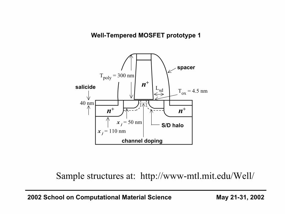
Well-Tempered MOSFET prototype 1
salicide
channel doping
S/D halo
n+ n+
Tox = 4.5 nm
x j = 50 nmx j = 110 nm
spacer
40 nm
Tpoly = 300 nm
Lsdn+
2002 School on Computational Material Science May 21-31, 2002
Sample structures at: http://www-mtl.mit.edu/Well/

90 nm Well-Tempered MOSFET doping profile
2002 School on Computational Material Science May 21-31, 2002

90 nm Well-Tempered MOSFET simulation conditions
A total of about 50,000 electrons are used in typicalsimulations.
Transport time-step is the same as the intervalbetween consecutive Poisson solutions, and was0.1 fs.
120,000 time steps simulated = 12 ps simulationtime. Data was collected after a transient of 50,000time step.
Wall clock time of simulation 8 hours on 16 CPUs.
2002 School on Computational Material Science May 21-31, 2002

90 nm Well-Tempered MOSFET – longitudinal field result
2002 School on Computational Material Science May 21-31, 2002
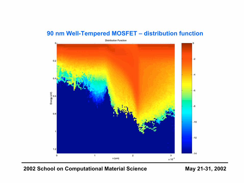
90 nm Well-Tempered MOSFET – distribution function
2002 School on Computational Material Science May 21-31, 2002

90 nm Well-Tempered MOSFET – electron density
2002 School on Computational Material Science May 21-31, 2002

90 nm Well-Tempered MOSFET – Test of P3M short range calculations
2002 School on Computational Material Science May 21-31, 2002

90 nm Well-Tempered MOSFET – Test of P3M short range calculations
• Communication pattern between nodes changessignificantly because of the different coupling, whencharge-charge interaction is included. This affects the runtime of the simulation. Additional domain decompositionstrategies may be necessary.
• Results with and without P3M are similar, except for a smallamount of heating caused by the additional short rangeforces. This means that the fine Poisson mesh used is veryeffective for this channel length and regime of operation.
• With P3M the Poisson mesh can be coarsened to reduceoverall simulation cost.
2002 School on Computational Material Science May 21-31, 2002

90 nm Well-Tempered MOSFET – Test of P3M short range calculations
• The particle-particle interaction introduces additional dataexchanges among nodes, reducing the overall performanceof the code. The short range interaction radius is chosen tobe minimum distance which spans two mesh cells in anydirection.
• If the slice thickness in the domain decomposition is set tofour meshes, information on all the particles in the domainmust be reported to the neighboring nodes on either side ofthe slice, as all particles are within the short-rangeinteraction radius from the domain interfaces.
• As a result the runtime performance of the code sufferssignificantly in parallel mode, with 2 to 3 times increase inexecution cost.
2002 School on Computational Material Science May 21-31, 2002

90 nm Well-Tempered MOSFET – Test of P3M short range calculations
• In the device simulation presented, dopants arestill treated as smooth varying functions ofpositions. Charge-ion interaction is includedusing scattering rates.
• Granular dopant can be included simply, sincethe P3M method treats electron-ion interaction inthe same way as electron-electron interaction.
• Granularity will be important in very smalldevices. For instance, if the channel density is1019 cm-3 average ion distance is about 5 nm.Only a few channel ions would be on the path of aparticle.
2002 School on Computational Material Science May 21-31, 2002

Monte Carlo simulation of Schottky barrier MOSFET(Winstead and Ravaioli, IEEE TED, vol. 47, p. 1241, 2001)
Quantum injection through the contacts is coupled to semi-classical Monte Carlo.
2002 School on Computational Material Science May 21-31, 2002

Monte Carlo simulation of Schottky barrier MOSFET
2002 School on Computational Material Science May 21-31, 2002

Monte Carlo simulation of Schottky barrier MOSFET
The silicide contacts are modeled as ideal metals. A distribution ofinjected particles is obtained statistically by using a transmissionprobability across the Schottky barrier, calculated a set of 1-DSchrödinger equations using the Airy function approach.
2002 School on Computational Material Science May 21-31, 2002

Monte Carlo simulation of Schottky barrier MOSFET
The particles in the contacts are not simulated explicitly, therefore thechannel resolution is very good and subthreshold characteristics canbe resolved clearly.
[1] C. Wang, J.P. Snyder and J.R. Tucker, Appl. Phys. Lett., vol. 74, pp. 1174-1176, 1999.
2002 School on Computational Material Science May 21-31, 2002
Recommended