ARL-TR-7350 JULY 2015
US Army Research Laboratory
General Atomics Pulsed Power Capacitor Comparison Test Report
by Richard L Thomas Approved for public release; distribution unlimited.

NOTICES
Disclaimers The findings in this report are not to be construed as an official Department of the Army position unless so designated by other authorized documents.
Citation of manufacturer’s or trade names does not constitute an official endorsement or approval of the use thereof.
Destroy this report when it is no longer needed. Do not return it to the originator.
ARL-TR-7350 JULY 2015
US Army Research Laboratory
General Atomics Pulsed Power Capacitor Comparison Test Report
by Richard L Thomas Sensors and Electron Devices Directorate, ARL Approved for public release; distribution unlimited.
ii
REPORT DOCUMENTATION PAGE Form Approved OMB No. 0704-0188
Public reporting burden for this collection of information is estimated to average 1 hour per response, including the time for reviewing instructions, searching existing data sources, gathering and maintaining the data needed, and completing and reviewing the collection information. Send comments regarding this burden estimate or any other aspect of this collection of information, including suggestions for reducing the burden, to Department of Defense, Washington Headquarters Services, Directorate for Information Operations and Reports (0704-0188), 1215 Jefferson Davis Highway, Suite 1204, Arlington, VA 22202-4302. Respondents should be aware that notwithstanding any other provision of law, no person shall be subject to any penalty for failing to comply with a collection of information if it does not display a currently valid OMB control number. PLEASE DO NOT RETURN YOUR FORM TO THE ABOVE ADDRESS.
1. REPORT DATE (DD-MM-YYYY)
July 2015 2. REPORT TYPE
Final 3. DATES COVERED (From - To)
4. TITLE AND SUBTITLE
General Atomics Pulsed Power Capacitor Comparison Test Report 5a. CONTRACT NUMBER
5b. GRANT NUMBER
5c. PROGRAM ELEMENT NUMBER
6. AUTHOR(S)
Richard L Thomas 5d. PROJECT NUMBER
5e. TASK NUMBER
5f. WORK UNIT NUMBER
7. PERFORMING ORGANIZATION NAME(S) AND ADDRESS(ES)
US Army Research Laboratory ATTN: RDRL-SED-P 2800 Powder Mill Road Adelphi, MD 20783-1138
8. PERFORMING ORGANIZATION REPORT NUMBER
ARL-TR-7350
9. SPONSORING/MONITORING AGENCY NAME(S) AND ADDRESS(ES)
10. SPONSOR/MONITOR'S ACRONYM(S)
11. SPONSOR/MONITOR'S REPORT NUMBER(S)
12. DISTRIBUTION/AVAILABILITY STATEMENT
Approved for public release; distribution unlimited.
13. SUPPLEMENTARY NOTES
14. ABSTRACT
The advancement of the Army’s electronic lethality and survivability programs require energy dense capacitors that are capable of being discharged at a rate greater than 20 kA/μs and handle a voltage reversal of 20% of the rated charge voltage. The electrical and mechanical stresses of these requirements inherently cause capacitance loss during the discharge of the capacitor under test. The US Army Research Laboratory (ARL), in conjunction with General Atomics (GA), has been working to develop state of the art metalized polypropylene (MPP) capacitors that can withstand the stresses of operating in pulse power systems. This report discusses the pulse power test results of various MPP capacitors developed by GA and evaluated by ARL with the goal of maintaining 90% capacitance after enduring 10 charge and discharge cycles where the discharge occurs within tens of microseconds and the peak currents exceed 100 kA. Over the past decade, design advancements have been made that yield MPP capacitors with long DC life and high energy density but are also capable of discharge currents and rise times typically reserved for discrete foil capacitors. 15. SUBJECT TERMS
Capacitor, EMA, high energy storage
16. SECURITY CLASSIFICATION OF: 17. LIMITATION OF ABSTRACT
UU
18. NUMBER OF PAGES
20
19a. NAME OF RESPONSIBLE PERSON
Richard L Thomas a. REPORT
Unclassified b. ABSTRACT
Unclassified c. THIS PAGE
Unclassified 19b. TELEPHONE NUMBER (Include area code)
301-394-2936 Standard Form 298 (Rev. 8/98) Prescribed by ANSI Std. Z39.18
iii
Contents
List of Figures iv
List of Tables iv
1. Introduction 1
2. Capacitor Evaluation Circuit 1
3. Results and Discussion 2
3.1 Capacitor 38300-84 2
3.2 Capacitor 38382-88 4
3.3 Capacitor 38382-88WC 11
4. Conclusion 13
Distribution List 14
iv
List of Figures
Fig. 1 Test circuit ................................................................................................2
Fig. 2 Cap 0061 discharge 1 vs. discharge 13 .....................................................2
Fig. 3 Cap 0064 discharge 1 vs. discharge 8 .......................................................3
Fig. 4 Cap 0057 discharge 1 vs. discharge 8 .......................................................3
Fig. 5 Cap characteristic change over discharge life ...........................................3
Fig. 6 Cap 8 low inductance discharge 1vs. discharge 140.................................4
Fig. 7 Medium inductance discharge 2 vs. discharge 21 ....................................4
Fig. 8 Voltage stress on the capacitor ..................................................................5
Fig. 9 Current stress on the capacitor ..................................................................5
Fig. 10 Objective buss vs. BAE evaluation buss ...................................................6
Fig. 11 High voltage reversal test ..........................................................................7
Fig. 12 Voltage stress on Cap 8 .............................................................................7
Fig. 13 Current stress on Cap 8 .............................................................................8
Fig. 14 Cap 8 voltage reversal ...............................................................................8
Fig. 15 High voltage reversal test failure ..............................................................9
Fig. 16 Cap 8 failure side view .............................................................................9
Fig. 17 Cap 8 failure rear angle view ..................................................................10
Fig. 18 Voltage stress on the Cap 9 .....................................................................10
Fig. 19 Current stress on the Cap 9 .....................................................................11
Fig. 20 Discharge waveform ...............................................................................12
Fig. 21 Cap 9 failure ............................................................................................12
Fig. 22 Cap 9 failure header close-up .................................................................13
List of Tables
Table 1 Capacitance and dissipation factor vs. number of discharge .....................7
Table 2 The 2-min voltage drop ...........................................................................11

1
1. Introduction
The advancement of the Army’s electronic lethality and survivability programs requires energy-dense capacitors that are capable of being discharged at a rate greater than 20 kA/µs and can handle a voltage reversal of 20% of the rated charge voltage. The stresses of these requirements inherently cause capacitance loss during the discharge of the capacitor under test. The guideline for the acceptability of a capacitor under theses test conditions is that the capacitor does not lose more than 10% of its original capacitance after 10 charge and discharge cycles.
General Atomics (GA) has been developing capacitors to meet the demand of these requirements. The latest 3 models of capacitors were tested and their performance is being evaluated to identify a viable candidate for the use in various high voltage applications.
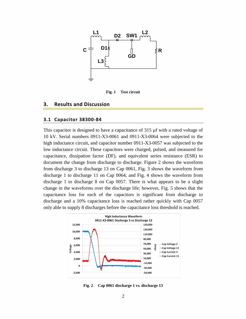
2. Capacitor Evaluation Circuit
To properly evaluate how the capacitor will respond to load variations outside of the system, the testbed described in the circuit shown in Fig. 1 was used. This circuit comprises the device under test C, buss inductance L1, adjustable inductances L2 and L3, anti-parallel diode D1, series diode D2, high current switch SW1, and adjustable resistance R. There are 2 extreme waveform characteristics that are used to vet the capacitors. The first of these 2 waveforms is a low inductive load path, which will produce a waveform with a rate of rise greater than 20 kA/µs and no voltage reversal on the capacitor. This requires the circuit to have approximately 70 nH of inductance for L2 and 10 nH for L3 with R at 33 mohm. The other waveform requires a much lower rate of rise but produces a 20% voltage reversal on the capacitor and a much longer current pulse. This requires the circuit load to have approximately 700 nH of inductance for L2 and no change with L3 with R equal to 25 mohms. The test circuit has a buss that can adjust the distance between the buss, thus varying the inductance to the desired level. The reconfigurable load bank consists of 9 different paralleled stacks of 0.1 ohm resistors that can hold up to 0.4 ohms.
2
C
L1 D2
D1
L3
SW1 L2
RGD
Fig. 1 Test circuit
3. Results and Discussion
3.1 Capacitor 38300-84
This capacitor is designed to have a capacitance of 315 µf with a rated voltage of 10 kV. Serial numbers 0911-X3-0061 and 0911-X3-0064 were subjected to the high inductance circuit, and capacitor number 0911-X3-0057 was subjected to the low inductance circuit. These capacitors were charged, pulsed, and measured for capacitance, dissipation factor (DF), and equivalent series resistance (ESR) to document the change from discharge to discharge. Figure 2 shows the waveform from discharge 3 to discharge 13 on Cap 0061, Fig. 3 shows the waveform from discharge 1 to discharge 11 on Cap 0064, and Fig. 4 shows the waveform from discharge 1 to discharge 8 on Cap 0057. There is what appears to be a slight change in the waveforms over the discharge life; however, Fig. 5 shows that the capacitance loss for each of the capacitors is significant from discharge to discharge and a 10% capacitance loss is reached rather quickly with Cap 0057 only able to supply 8 discharges before the capacitance loss threshold is reached.
Fig. 2 Cap 0061 discharge 1 vs. discharge 13
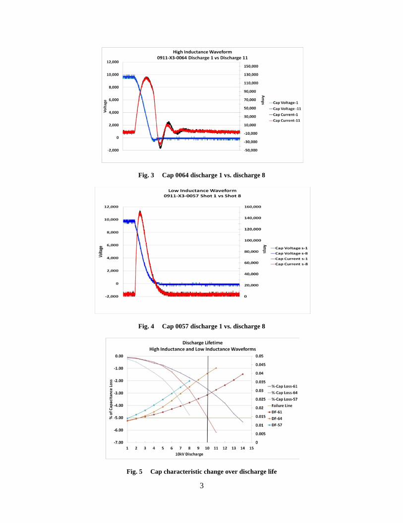
3
Fig. 3 Cap 0064 discharge 1 vs. discharge 8
Fig. 4 Cap 0057 discharge 1 vs. discharge 8
Fig. 5 Cap characteristic change over discharge life
4
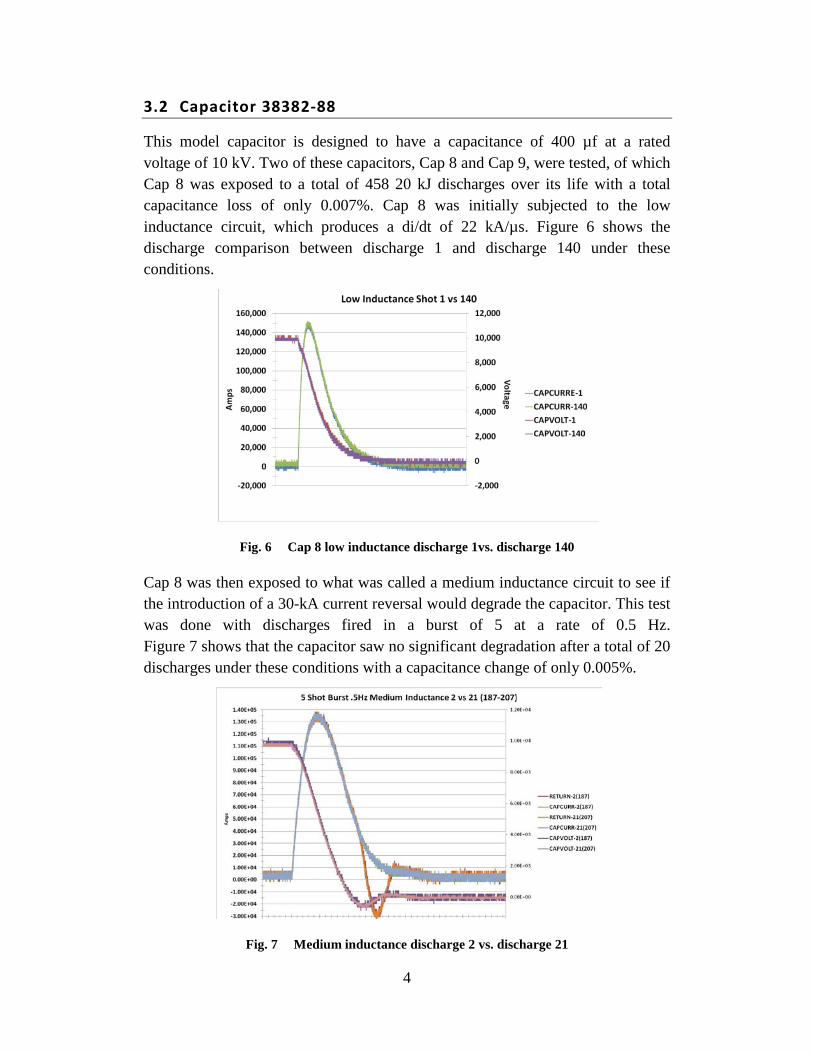
3.2 Capacitor 38382-88
This model capacitor is designed to have a capacitance of 400 µf at a rated voltage of 10 kV. Two of these capacitors, Cap 8 and Cap 9, were tested, of which Cap 8 was exposed to a total of 458 20 kJ discharges over its life with a total capacitance loss of only 0.007%. Cap 8 was initially subjected to the low inductance circuit, which produces a di/dt of 22 kA/µs. Figure 6 shows the discharge comparison between discharge 1 and discharge 140 under these conditions.
Fig. 6 Cap 8 low inductance discharge 1vs. discharge 140
Cap 8 was then exposed to what was called a medium inductance circuit to see if the introduction of a 30-kA current reversal would degrade the capacitor. This test was done with discharges fired in a burst of 5 at a rate of 0.5 Hz. Figure 7 shows that the capacitor saw no significant degradation after a total of 20 discharges under these conditions with a capacitance change of only 0.005%.
Fig. 7 Medium inductance discharge 2 vs. discharge 21
5
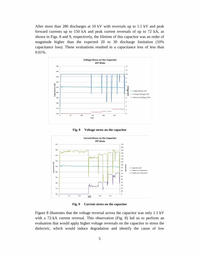
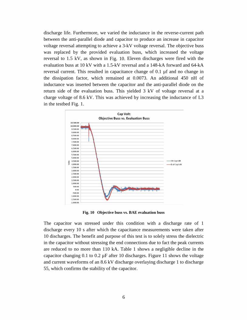
After more than 280 discharges at 10 kV with reversals up to 1.1 kV and peak forward currents up to 150 kA and peak current reversals of up to 72 kA, as shown in Figs. 8 and 9, respectively, the lifetime of this capacitor was an order of magnitude higher than the expected 20 to 30 discharge limitation (10% capacitance loss). These evaluations resulted in a capacitance loss of less than 0.01%.
Fig. 8 Voltage stress on the capacitor
Fig. 9 Current stress on the capacitor
Figure 8 illustrates that the voltage reversal across the capacitor was only 1.1 kV with a 72-kA current reversal. This observation (Fig. 8) led us to perform an evaluation that would apply higher voltage reversals on the capacitor to stress the dielectric, which would induce degradation and identify the cause of low
6
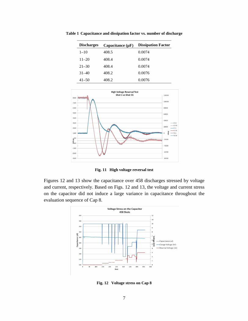
discharge life. Furthermore, we varied the inductance in the reverse-current path between the anti-parallel diode and capacitor to produce an increase in capacitor voltage reversal attempting to achieve a 3-kV voltage reversal. The objective buss was replaced by the provided evaluation buss, which increased the voltage reversal to 1.5 kV, as shown in Fig. 10. Eleven discharges were fired with the evaluation buss at 10 kV with a 1.5-kV reversal and a 148-kA forward and 64-kA reversal current. This resulted in capacitance change of 0.1 µf and no change in the dissipation factor, which remained at 0.0073. An additional 450 nH of inductance was inserted between the capacitor and the anti-parallel diode on the return side of the evaluation buss. This yielded 3 kV of voltage reversal at a charge voltage of 8.6 kV. This was achieved by increasing the inductance of L3 in the testbed Fig. 1.
Fig. 10 Objective buss vs. BAE evaluation buss
The capacitor was stressed under this condition with a discharge rate of 1 discharge every 10 s after which the capacitance measurements were taken after 10 discharges. The benefit and purpose of this test is to solely stress the dielectric in the capacitor without stressing the end connections due to fact the peak currents are reduced to no more than 110 kA. Table 1 shows a negligible decline in the capacitor changing 0.1 to 0.2 µF after 10 discharges. Figure 11 shows the voltage and current waveforms of an 8.6 kV discharge overlaying discharge 1 to discharge 55, which confirms the stability of the capacitor.
7
Table 1 Capacitance and dissipation factor vs. number of discharge
Discharges
Capacitance (µF)
Dissipation Factor
1–10
408.5
0.0074
11–20
408.4
0.0074
21–30
408.4
0.0074
31–40
408.2
0.0076
41–50
408.2
0.0076
Fig. 11 High voltage reversal test
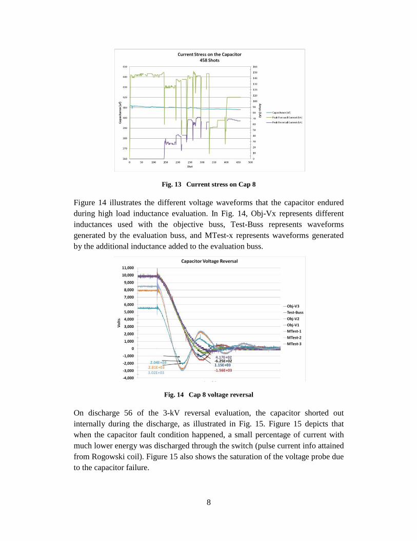
Figures 12 and 13 show the capacitance over 458 discharges stressed by voltage and current, respectively. Based on Figs. 12 and 13, the voltage and current stress on the capacitor did not induce a large variance in capacitance throughout the evaluation sequence of Cap 8.
Fig. 12 Voltage stress on Cap 8
8
Fig. 13 Current stress on Cap 8
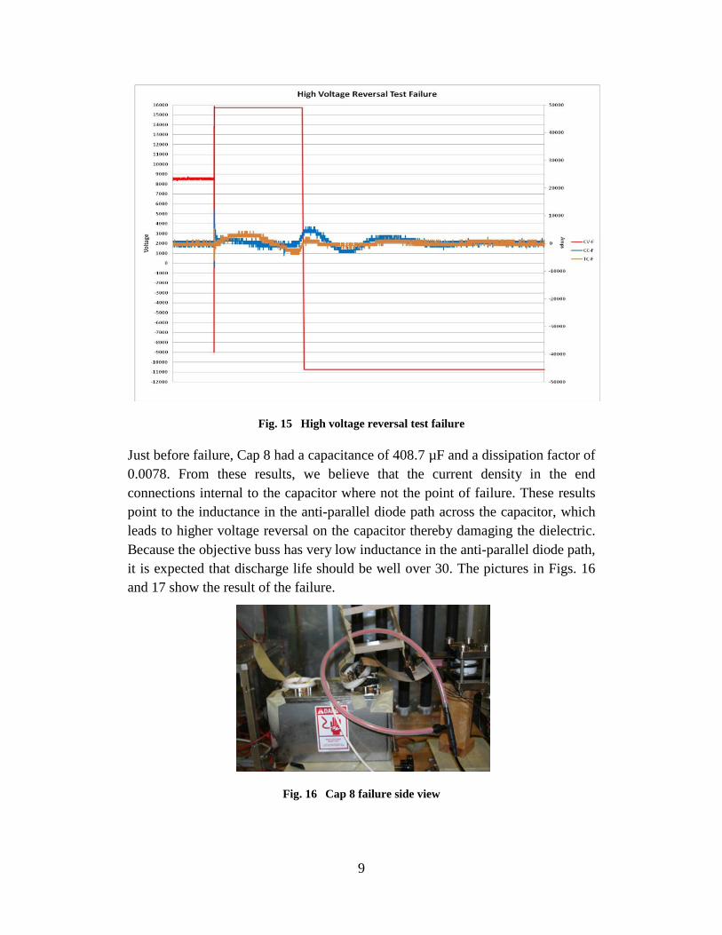
Figure 14 illustrates the different voltage waveforms that the capacitor endured during high load inductance evaluation. In Fig. 14, Obj-Vx represents different inductances used with the objective buss, Test-Buss represents waveforms generated by the evaluation buss, and MTest-x represents waveforms generated by the additional inductance added to the evaluation buss.
Fig. 14 Cap 8 voltage reversal
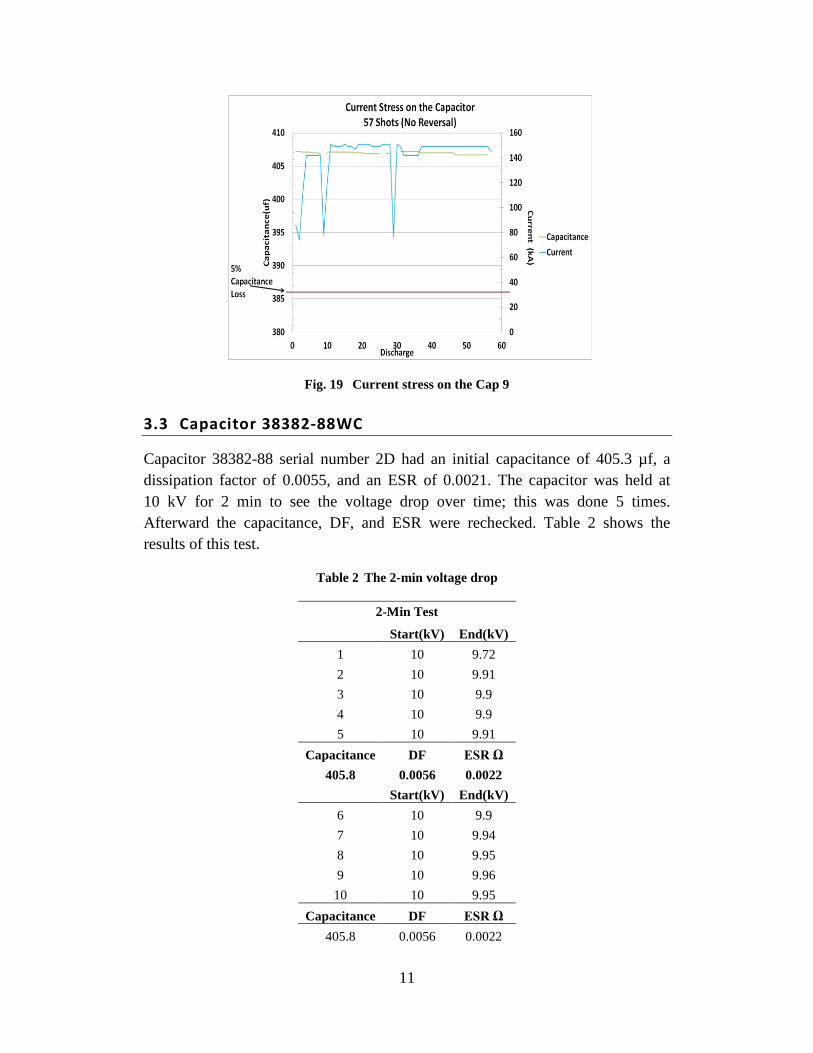
On discharge 56 of the 3-kV reversal evaluation, the capacitor shorted out internally during the discharge, as illustrated in Fig. 15. Figure 15 depicts that when the capacitor fault condition happened, a small percentage of current with much lower energy was discharged through the switch (pulse current info attained from Rogowski coil). Figure 15 also shows the saturation of the voltage probe due to the capacitor failure.
9
Fig. 15 High voltage reversal test failure
Just before failure, Cap 8 had a capacitance of 408.7 µF and a dissipation factor of 0.0078. From these results, we believe that the current density in the end connections internal to the capacitor where not the point of failure. These results point to the inductance in the anti-parallel diode path across the capacitor, which leads to higher voltage reversal on the capacitor thereby damaging the dielectric. Because the objective buss has very low inductance in the anti-parallel diode path, it is expected that discharge life should be well over 30. The pictures in Figs. 16 and 17 show the result of the failure.
Fig. 16 Cap 8 failure side view

10
Fig. 17 Cap 8 failure rear angle view
Cap 9 was tested in the low inductance circuit with 25 discharges single discharge and then 25 discharges in a burst of 5 at a rate of 0.4 Hz. Figures 18 and 19 show the capacitance loss with respect to the voltage and current stresses respectively. It is clear that Cap 9 is following the trend of Cap 8. Further testing on Cap 9 will take place with other system component integration.
Fig. 18 Voltage stress on the Cap 9
11
Fig. 19 Current stress on the Cap 9
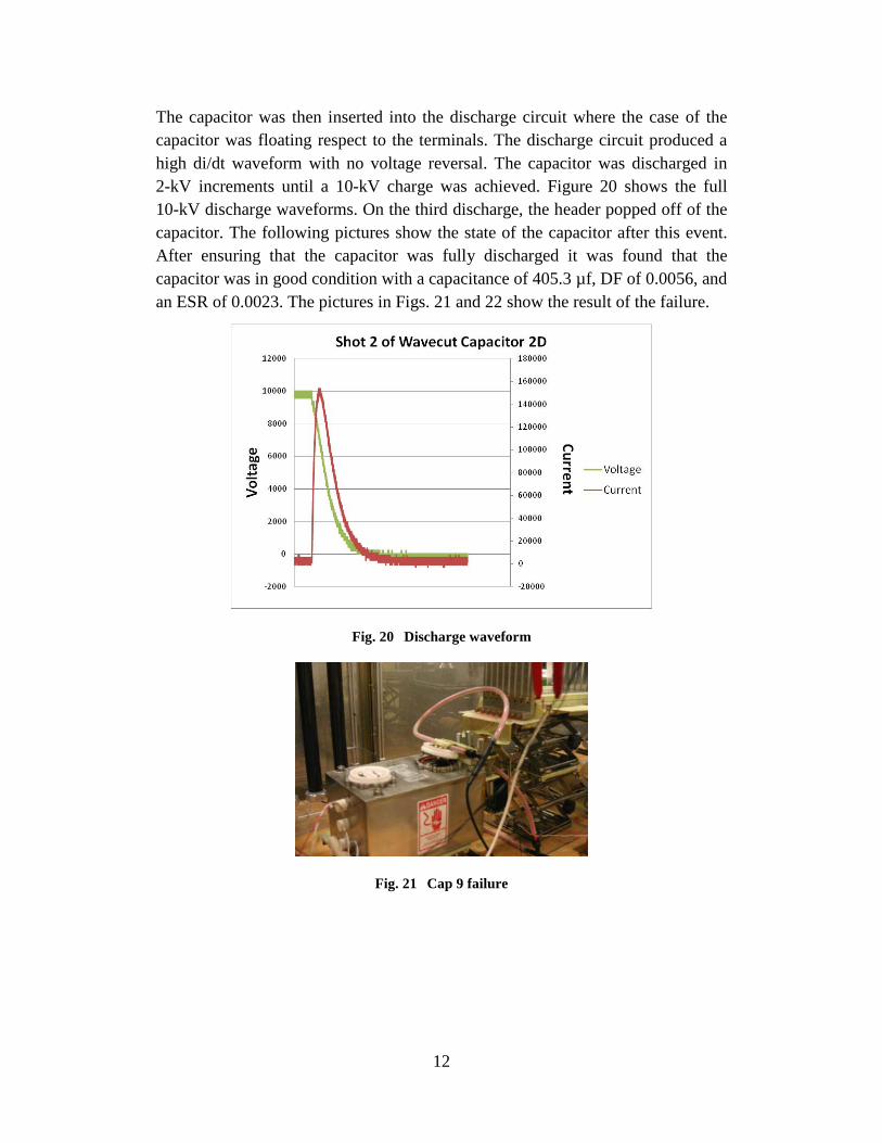
3.3 Capacitor 38382-88WC
Capacitor 38382-88 serial number 2D had an initial capacitance of 405.3 µf, a dissipation factor of 0.0055, and an ESR of 0.0021. The capacitor was held at 10 kV for 2 min to see the voltage drop over time; this was done 5 times. Afterward the capacitance, DF, and ESR were rechecked. Table 2 shows the results of this test.
Table 2 The 2-min voltage drop
2-Min Test
Start(kV) End(kV)
1 10 9.72 2 10 9.91 3 10 9.9 4 10 9.9 5 10 9.91
Capacitance DF ESR Ω 405.8 0.0056 0.0022
Start(kV) End(kV)
6 10 9.9 7 10 9.94 8 10 9.95 9 10 9.96
10 10 9.95 Capacitance DF ESR Ω
405.8 0.0056 0.0022
12
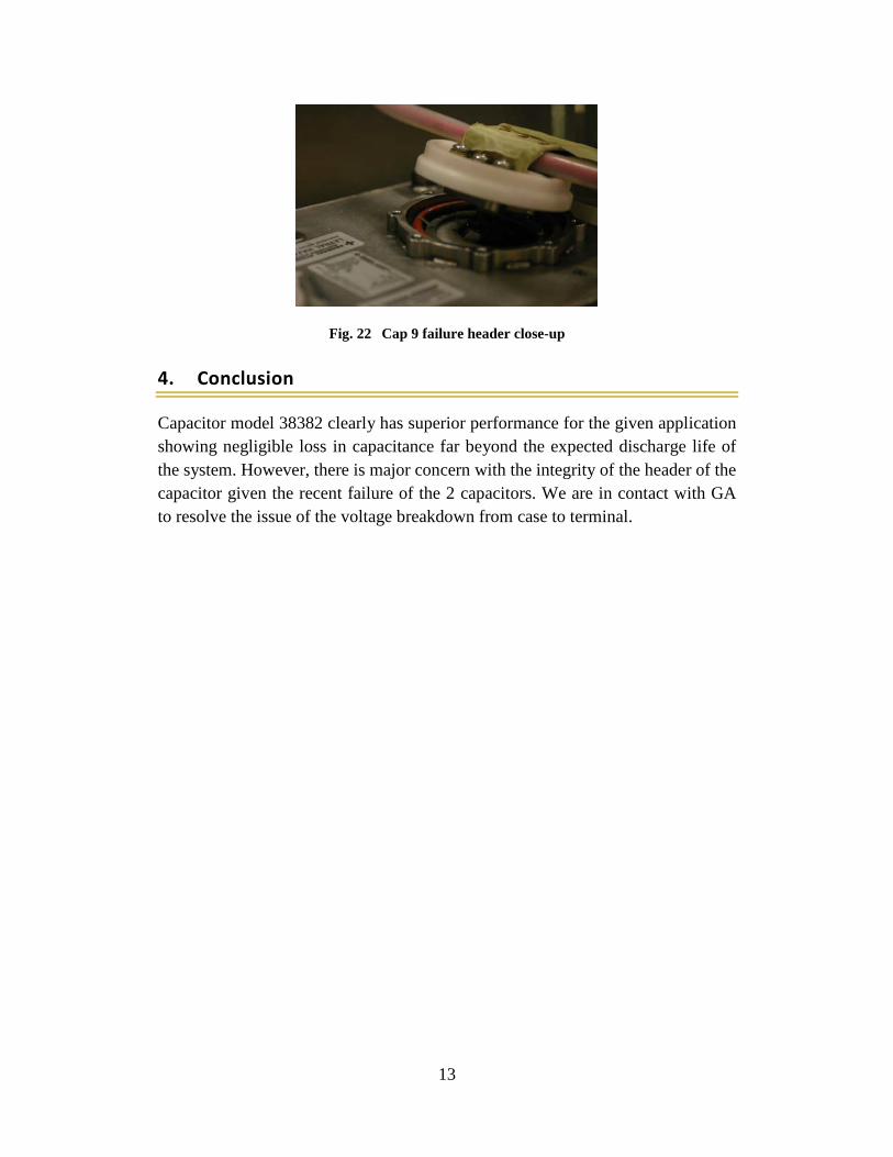
The capacitor was then inserted into the discharge circuit where the case of the capacitor was floating respect to the terminals. The discharge circuit produced a high di/dt waveform with no voltage reversal. The capacitor was discharged in 2-kV increments until a 10-kV charge was achieved. Figure 20 shows the full 10-kV discharge waveforms. On the third discharge, the header popped off of the capacitor. The following pictures show the state of the capacitor after this event. After ensuring that the capacitor was fully discharged it was found that the capacitor was in good condition with a capacitance of 405.3 µf, DF of 0.0056, and an ESR of 0.0023. The pictures in Figs. 21 and 22 show the result of the failure.
Fig. 20 Discharge waveform
Fig. 21 Cap 9 failure
13
Fig. 22 Cap 9 failure header close-up
4. Conclusion
Capacitor model 38382 clearly has superior performance for the given application showing negligible loss in capacitance far beyond the expected discharge life of the system. However, there is major concern with the integrity of the header of the capacitor given the recent failure of the 2 capacitors. We are in contact with GA to resolve the issue of the voltage breakdown from case to terminal.
14
1 DEFENSE TECH INFO CTR (PDF) ATTN DTIC OCA 2 US ARMY RSRCH LAB (PDF) ATTN IMAL HRA MAIL & RECORDS MGMT ATTN RDRL CIO LL TECHL LIB 1 GOVT PRNTG OFC (PDF) ATTN A MALHOTRA 2 US ARMY TARDEC (PDF) ATTN JOSEPH D WHITE ATTN STUART M DAVIS 1 GENERAL ATOMICS (PDF) ATTN JOEL ENNIS 5 US ARMY RSRCH LAB (PDF) ATTN RDRL SED C R JOW ATTN RDRL SED E C SHAFFER ATTN RDRL SED P C SCOZZIE M BERMAN R THOMAS
Recommended