High performance InGaZnO thin film transistor with InGaZnO source and drainelectrodesHung-Chi Wu and Chao-Hsin Chien
Citation: Applied Physics Letters 102, 062103 (2013); doi: 10.1063/1.4789997 View online: http://dx.doi.org/10.1063/1.4789997 View Table of Contents: http://scitation.aip.org/content/aip/journal/apl/102/6?ver=pdfcov Published by the AIP Publishing Articles you may be interested in Mobility enhancement in amorphous InGaZnO thin-film transistors by Ar plasma treatment Appl. Phys. Lett. 102, 222103 (2013); 10.1063/1.4809727 Electrical characterization of a-InGaZnO thin-film transistors with Cu source/drain electrodes Appl. Phys. Lett. 100, 112109 (2012); 10.1063/1.3694273 Correlation of photoconductivity response of amorphous In–Ga–Zn–O films with transistor performance usingmicrowave photoconductivity decay method Appl. Phys. Lett. 98, 102107 (2011); 10.1063/1.3561755 Nitrogenated amorphous InGaZnO thin film transistor Appl. Phys. Lett. 98, 052102 (2011); 10.1063/1.3551537 Fully transparent InGaZnO thin film transistors using indium tin oxide/graphene multilayer as source/drainelectrodes Appl. Phys. Lett. 97, 172106 (2010); 10.1063/1.3490245
This article is copyrighted as indicated in the article. Reuse of AIP content is subject to the terms at: http://scitation.aip.org/termsconditions. Downloaded to IP:
140.113.38.11 On: Thu, 01 May 2014 01:04:10
High performance InGaZnO thin film transistor with InGaZnO sourceand drain electrodes
Hung-Chi Wu1 and Chao-Hsin Chien2,a)
1Department of Electronics Engineering and Institute of Electronics, National Chiao Tung University,Hsinchu, Taiwan2Department of Electronics Engineering and Institute of Electronics, National Chiao Tung University,Hsinchu, Taiwan and National Nano Device Laboratories, Hsinchu, Taiwan
(Received 23 October 2012; accepted 17 January 2013; published online 11 February 2013)
This work demonstrates In-Ga-Zn-O (IGZO) as source and drain electrodes in IGZO-thin
film transistors (TFTs). The fabricated TFT depicts excellent electrical properties; its mobility is
18.02 (cm2/V s), threshold voltage (Vth) is 0.3 (V), on/off ratio is 1.63� 108 and subthreshold swing
(S.S.) is 239 (mV/decade). We find using rapid thermal annealing treatment can convert IGZO into an
effective conductor, and the transparency of IGZO remained almost unchanged. We also find
sufficient thermal budget is needed for getting stable transfer curve and output characteristic;
otherwise, current fluctuation in on-state can be easily observed. With IGZO electrodes, fully
transparent IGZO-TFTs can be thus realized on a glass substrate. VC 2013 American Institute ofPhysics. [http://dx.doi.org/10.1063/1.4789997]
Amorphous oxide semiconductors (AOS) have attracted
industrial and commercial interests in recent years. Their
advantages include low temperature process, large area fabri-
cation, low cost, and compatibility with flexible electronics.1
Its wide application to the flexible electronics, thin film tran-
sistors (TFTs), electronic papers, and sensors make AOS
have the possibility to become the mainstream channel mate-
rial for the next generation TFTs.2,3 Among several AOS
materials, In-Ga-Zn-O (IGZO) is one of the most promising
candidates. The TFTs with IGZO usually exhibit more supe-
rior electrical properties than those with amorphous silicon,
poly-silicon, and organic conjugated polymers in terms of
channel mobility, on/off ratio, subthreshold swing (S.S.), and
threshold voltage (Vth).4,5 Moreover, IGZO thin film is trans-
parent since its plasma frequency lies in the infrared region.6
This feature facilitates the production of transparent display,
detectors, and other applications.7,8 Even so, the IGZO-TFTs
are not fully transparent since they need nontransparent
metal as the source and drain electrodes. The presence of
metal source and drain will certainly deteriorate the transpar-
ency since metals are opaque. Although indium-tin-oxide
(ITO) is reported to be a good transparent electrode, the
transparency of ITO is very sensitive to the process condition
and post deposition treatment.
In this work, we demonstrate the possibility of making
high performance IGZO-TFTs with IGZO source and drain
electrodes. We find that rapid thermal annealing (RTA) can
convert the IGZO thin film into an effective conductor. With
sufficient thermal budget our fabricated IGZO-TFTs with
IGZO source and drain electrodes depict excellent electrical
properties in terms of mobility, threshold voltage, and on/off
ratio. Certainly, the transparency has been improved by
replacing metal source and drain electrodes. Our results sug-
gest the fabrication of highly transparent IGZO-TFTs with
non-metal electrodes is feasible.
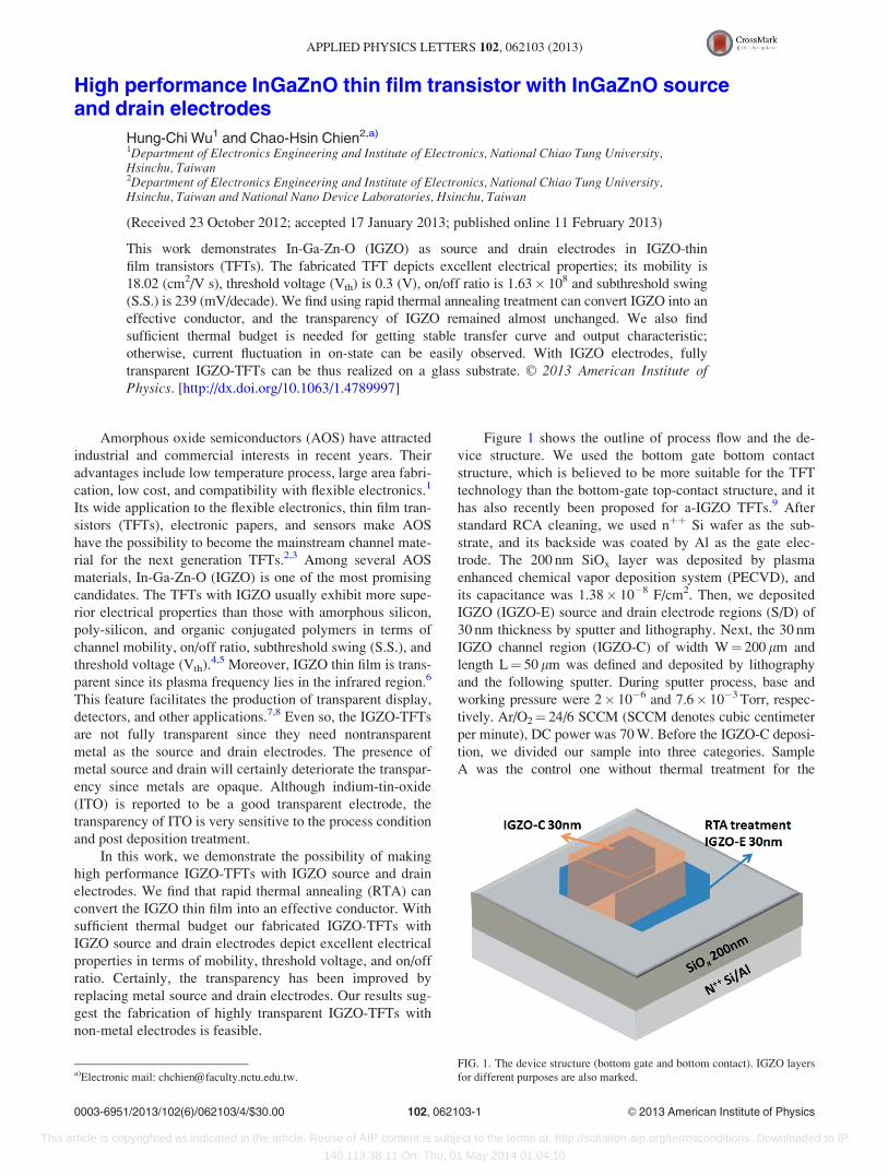
Figure 1 shows the outline of process flow and the de-
vice structure. We used the bottom gate bottom contact
structure, which is believed to be more suitable for the TFT
technology than the bottom-gate top-contact structure, and it
has also recently been proposed for a-IGZO TFTs.9 After
standard RCA cleaning, we used nþþ Si wafer as the sub-
strate, and its backside was coated by Al as the gate elec-
trode. The 200 nm SiOx layer was deposited by plasma
enhanced chemical vapor deposition system (PECVD), and
its capacitance was 1.38� 10�8 F/cm2. Then, we deposited
IGZO (IGZO-E) source and drain electrode regions (S/D) of
30 nm thickness by sputter and lithography. Next, the 30 nm
IGZO channel region (IGZO-C) of width W¼ 200 lm and
length L¼ 50 lm was defined and deposited by lithography
and the following sputter. During sputter process, base and
working pressure were 2� 10�6 and 7.6� 10�3 Torr, respec-
tively. Ar/O2¼ 24/6 SCCM (SCCM denotes cubic centimeter
per minute), DC power was 70 W. Before the IGZO-C deposi-
tion, we divided our sample into three categories. Sample
A was the control one without thermal treatment for the
FIG. 1. The device structure (bottom gate and bottom contact). IGZO layers
for different purposes are also marked.a)Electronic mail: [email protected].
0003-6951/2013/102(6)/062103/4/$30.00 VC 2013 American Institute of Physics102, 062103-1
APPLIED PHYSICS LETTERS 102, 062103 (2013)
This article is copyrighted as indicated in the article. Reuse of AIP content is subject to the terms at: http://scitation.aip.org/termsconditions. Downloaded to IP:
140.113.38.11 On: Thu, 01 May 2014 01:04:10
IGZO-E, while sample B and C accepted RTA treatment in
N2 ambient at 400 �C before the deposition of IGZO-C. The
durations for RTA treatment were 30 and 60 s, respectively.
The electrical properties were measured by HP4156 semi-
conductor parameter analyzer, the drain voltage was set to
5 V, and the gate voltage was swept from �20 V to 20 V. We
also measured its output characteristics with varying drain
voltage from 0 V to 20 V and gate voltage 0 V to 20 V with a
step of 5 V. The thin film properties such as the composition
ratio and metal–oxygen bonding state was measured by X-ray
photoelectron spectroscopy (XPS), the optical transmission
measurement of the IGZO film was measured for wavelength
ranging from 300 to 800 nm by ultraviolet/visible/near infra-
red spectroscopy, and Hall effect measurements were per-
formed by Hall effect system at room temperature.
Figure 2 shows the transfer curves of samples. Table I
summaries the corresponding electrical parameters in this
work and other IGZO TFTs with various S/D electrodes. We
employed the current model of the conventional Si metal-ox-
ide-semiconductor field-effect-transistor (MOSFET),15 and
the expression is as follows:
ID ¼WlC
LVG � Vthð ÞVD �
V2D
2
� �ðlinear regimeÞ:
Hence the mobility was extracted according to l ¼ LWCVD
@ID
@VG: In addition, the S.S. was extracted from the linear por-
tion of the transfer curve by
S:S: ¼ @VG
@ log ID
;
where W is the transistor channel width, L is the transistor
channel length, C is the capacitance per unit area of the gate
insulator (SiO2), l is the field-effect mobility, ID, VD, and VG
are the drain current, drain, and gate voltage, respectively.
Sample A depicts acceptable Vth value and on/off
ratio but poor S.S. Especially, the mobility is of only about
1 cm2/V s. Moreover, there is an abnormal current behavior
between �3 V and 10 V and a reduction of on-current with
increased gate voltage. These results mean the carriers cannot
be effectively injected from the electrode into the channel.
However, sample B and C show steeper S.S., much higher mo-
bility, which achieves the standard of IGZO application, and
more impressive on/off ratio than sample A. Also, both sample
B and C do not have the abnormal current behavior before the
transistors are turned on. These results suggest that the RTA
treatment can transform the IGZO-E into an effective conduc-
tor. As a result, we can make high performance IGZO-TFTs
without metal source and drain electrodes. As compared with
the reported IGZO-TFTs in Table I, we consider the properties
of our devices are comparable with those of the conventional
IGZO-TFTs with metal electrodes. This approach can obvi-
ously enhance the transparency of TFTs and, more impor-
tantly, is fully comparable with the conventional IGZO-TFT
with metal electrodes processing. Fig. 3 shows ID�VD output
characteristics of sample B and C. We observe the curves of
sample B are not very stable. There is apparent current oscilla-
tion at high gate and drain voltages. In contrast, sample C
shows very stable and smooth curves at the whole applied volt-
age range. This implies that the duration of RTA shall be long
enough to convert the IGZO-E into an effective conductor. In
other words, the thermal budget shall be sufficient for well
transformation of IGZO from a semiconductor into an effec-
tive conductor.
FIG. 2. ID–VG transfer curves of samples A, B, and C.
TABLE I. Comparison of the various electrical parameters of our IGZO-
TFTs with those of the reported IGZO-TFTs with various metal electrodes.
S/D material Vth (V)
Mobility
(cm2/V s)
S.S.
(V/decade)
On/off
ratio
IGZO sample A �4.1 1.1 0.695 4.42� 106
IGZO sample B �0.8 5.53 0.193 9.42� 107
IGZO sample C 0.3 18.02 0.239 1.63� 108
Cu10 N/A 8.3 0.43 >108
Mo11 4.87 8.9 0.096 1.5� 1010
Ti/Au12 �0.92 10.2 0.13 2.2� 106
AZO13 0.6 13.7 0.25 4.7� 106
Mo/nþ IGZO14 0.2 5 0.2 �107
FIG. 3. ID�VD output characteristics of
sample B and C as a function of gate
voltage.
062103-2 H.-C. Wu and C.-H. Chien Appl. Phys. Lett. 102, 062103 (2013)
This article is copyrighted as indicated in the article. Reuse of AIP content is subject to the terms at: http://scitation.aip.org/termsconditions. Downloaded to IP:
140.113.38.11 On: Thu, 01 May 2014 01:04:10
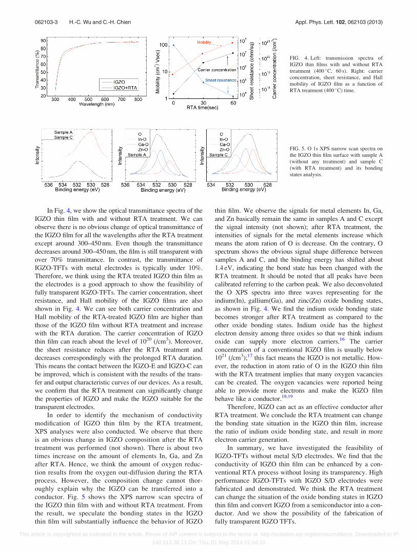
In Fig. 4, we show the optical transmittance spectra of the
IGZO thin film with and without RTA treatment. We can
observe there is no obvious change of optical transmittance of
the IGZO film for all the wavelengths after the RTA treatment
except around 300–450 nm. Even though the transmittance
decreases around 300–450 nm, the film is still transparent with
over 70% transmittance. In contrast, the transmittance of
IGZO-TFTs with metal electrodes is typically under 10%.
Therefore, we think using the RTA treated IGZO thin film as
the electrodes is a good approach to show the feasibility of
fully transparent IGZO-TFTs. The carrier concentration, sheet
resistance, and Hall mobility of the IGZO films are also
shown in Fig. 4. We can see both carrier concentration and
Hall mobility of the RTA-treated IGZO film are higher than
those of the IGZO film without RTA treatment and increase
with the RTA duration. The carrier concentration of IGZO
thin film can reach about the level of 1020 (/cm3). Moreover,
the sheet resistance reduces after the RTA treatment and
decreases correspondingly with the prolonged RTA duration.
This means the contact between the IGZO-E and IGZO-C can
be improved, which is consistent with the results of the trans-
fer and output characteristic curves of our devices. As a result,
we confirm that the RTA treatment can significantly change
the properties of IGZO and make the IGZO suitable for the
transparent electrodes.
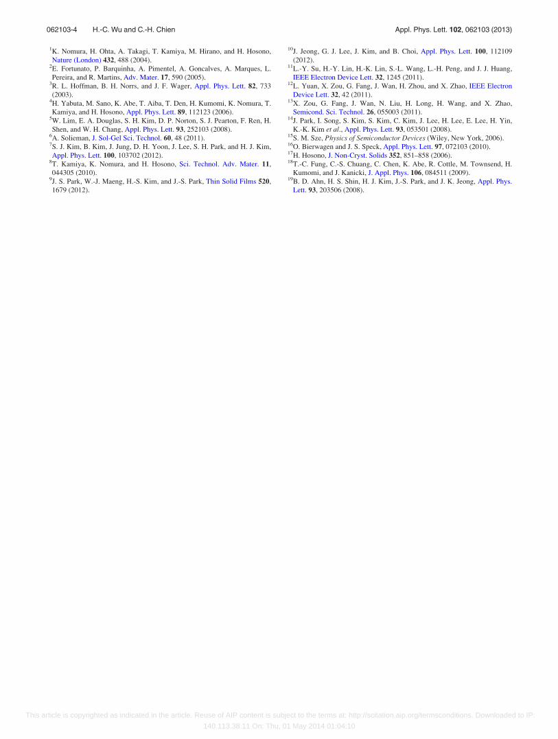
In order to identify the mechanism of conductivity
modification of IGZO thin film by the RTA treatment,
XPS analyses were also conducted. We observe that there
is an obvious change in IGZO composition after the RTA
treatment was performed (not shown). There is about two
times increase on the amount of elements In, Ga, and Zn
after RTA. Hence, we think the amount of oxygen reduc-
tion results from the oxygen out-diffusion during the RTA
process. However, the composition change cannot thor-
oughly explain why the IGZO can be transferred into a
conductor. Fig. 5 shows the XPS narrow scan spectra of
the IGZO thin film with and without RTA treatment. From
the result, we speculate the bonding states in the IGZO
thin film will substantially influence the behavior of IGZO
thin film. We observe the signals for metal elements In, Ga,
and Zn basically remain the same in samples A and C except
the signal intensity (not shown); after RTA treatment, the
intensities of signals for the metal elements increase which
means the atom ration of O is decrease. On the contrary, O
spectrum shows the obvious signal shape difference between
samples A and C, and the binding energy has shifted about
1.4 eV, indicating the bond state has been changed with the
RTA treatment. It should be noted that all peaks have been
calibrated referring to the carbon peak. We also deconvoluted
the O XPS spectra into three waves representing for the
indium(In), gallium(Ga), and zinc(Zn) oxide bonding states,
as shown in Fig. 4. We find the indium oxide bonding state
becomes stronger after RTA treatment as compared to the
other oxide bonding states. Indium oxide has the highest
electron density among three oxides so that we think indium
oxide can supply more electron carriers.16 The carrier
concentration of a conventional IGZO film is usually below
1021 (/cm3);17 this fact means the IGZO is not metallic. How-
ever, the reduction in atom ratio of O in the IGZO thin film
with the RTA treatment implies that many oxygen vacancies
can be created. The oxygen vacancies were reported being
able to provide more electrons and make the IGZO film
behave like a conductor.18,19
Therefore, IGZO can act as an effective conductor after
RTA treatment. We conclude the RTA treatment can change
the bonding state situation in the IGZO thin film, increase
the ratio of indium oxide bonding state, and result in more
electron carrier generation.
In summary, we have investigated the feasibility of
IGZO-TFTs without metal S/D electrodes. We find that the
conductivity of IGZO thin film can be enhanced by a con-
ventional RTA process without losing its transparency. High
performance IGZO-TFTs with IGZO S/D electrodes were
fabricated and demonstrated. We think the RTA treatment
can change the situation of the oxide bonding states in IGZO
thin film and convert IGZO from a semiconductor into a con-
ductor. And we show the possibility of the fabrication of
fully transparent IGZO TFTs.
FIG. 4. Left: transmission spectra of
IGZO thin films with and without RTA
treatment (400 �C, 60 s). Right: carrier
concentration, sheet resistance, and Hall
mobility of IGZO film as a function of
RTA treatment (400 �C) time.
FIG. 5. O 1s XPS narrow scan spectra on
the IGZO thin film surface with sample A
(without any treatment) and sample C
(with RTA treatment) and its bonding
states analysis.
062103-3 H.-C. Wu and C.-H. Chien Appl. Phys. Lett. 102, 062103 (2013)
This article is copyrighted as indicated in the article. Reuse of AIP content is subject to the terms at: http://scitation.aip.org/termsconditions. Downloaded to IP:
140.113.38.11 On: Thu, 01 May 2014 01:04:10
1K. Nomura, H. Ohta, A. Takagi, T. Kamiya, M. Hirano, and H. Hosono,
Nature (London) 432, 488 (2004).2E. Fortunato, P. Barquinha, A. Pimentel, A. Goncalves, A. Marques, L.
Pereira, and R. Martins, Adv. Mater. 17, 590 (2005).3R. L. Hoffman, B. H. Norrs, and J. F. Wager, Appl. Phys. Lett. 82, 733
(2003).4H. Yabuta, M. Sano, K. Abe, T. Aiba, T. Den, H. Kumomi, K. Nomura, T.
Kamiya, and H. Hosono, Appl. Phys. Lett. 89, 112123 (2006).5W. Lim, E. A. Douglas, S. H. Kim, D. P. Norton, S. J. Pearton, F. Ren, H.
Shen, and W. H. Chang, Appl. Phys. Lett. 93, 252103 (2008).6A. Solieman, J. Sol-Gel Sci. Technol. 60, 48 (2011).7S. J. Kim, B. Kim, J. Jung, D. H. Yoon, J. Lee, S. H. Park, and H. J. Kim,
Appl. Phys. Lett. 100, 103702 (2012).8T. Kamiya, K. Nomura, and H. Hosono, Sci. Technol. Adv. Mater. 11,
044305 (2010).9J. S. Park, W.-J. Maeng, H.-S. Kim, and J.-S. Park, Thin Solid Films 520,
1679 (2012).
10J. Jeong, G. J. Lee, J. Kim, and B. Choi, Appl. Phys. Lett. 100, 112109
(2012).11L.-Y. Su, H.-Y. Lin, H.-K. Lin, S.-L. Wang, L.-H. Peng, and J. J. Huang,
IEEE Electron Device Lett. 32, 1245 (2011).12L. Yuan, X. Zou, G. Fang, J. Wan, H. Zhou, and X. Zhao, IEEE Electron
Device Lett. 32, 42 (2011).13X. Zou, G. Fang, J. Wan, N. Liu, H. Long, H. Wang, and X. Zhao,
Semicond. Sci. Technol. 26, 055003 (2011).14J. Park, I. Song, S. Kim, S. Kim, C. Kim, J. Lee, H. Lee, E. Lee, H. Yin,
K.-K. Kim et al., Appl. Phys. Lett. 93, 053501 (2008).15S. M. Sze, Physics of Semiconductor Devices (Wiley, New York, 2006).16O. Bierwagen and J. S. Speck, Appl. Phys. Lett. 97, 072103 (2010).17H. Hosono, J. Non-Cryst. Solids 352, 851–858 (2006).18T.-C. Fung, C.-S. Chuang, C. Chen, K. Abe, R. Cottle, M. Townsend, H.
Kumomi, and J. Kanicki, J. Appl. Phys. 106, 084511 (2009).19B. D. Ahn, H. S. Shin, H. J. Kim, J.-S. Park, and J. K. Jeong, Appl. Phys.
Lett. 93, 203506 (2008).
062103-4 H.-C. Wu and C.-H. Chien Appl. Phys. Lett. 102, 062103 (2013)
This article is copyrighted as indicated in the article. Reuse of AIP content is subject to the terms at: http://scitation.aip.org/termsconditions. Downloaded to IP:
140.113.38.11 On: Thu, 01 May 2014 01:04:10
Recommended