External Use
Innovation to Advance Moore’s LawRequires Core Technology Revolution
UC Berkeley SeminarMarch 9th, 2012
Klaus Schuegraf, Ph.D.Chief Technology OfficerSilicon Systems GroupApplied Materials
External Use
Innovation to Advance Moore’s Law
Thank you for coming
2
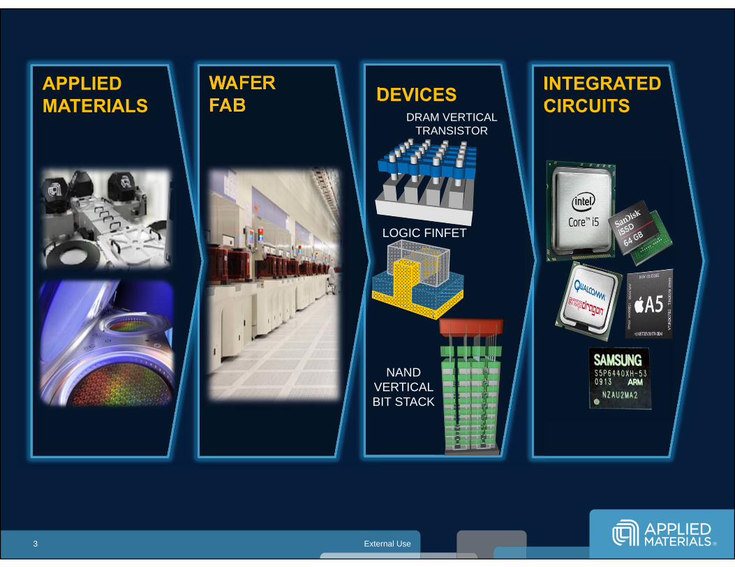
Semiconductor Value Chain - Equipment
Moore’s Law Challenges
Core Technology Focus
Opportunities for Innovation
External Use3
INTEGRATEDCIRCUITSDEVICESWAFER
FABAPPLIEDMATERIALS
NAND VERTICAL BIT STACK
DRAM VERTICAL TRANSISTOR
LOGIC FINFET
External Use
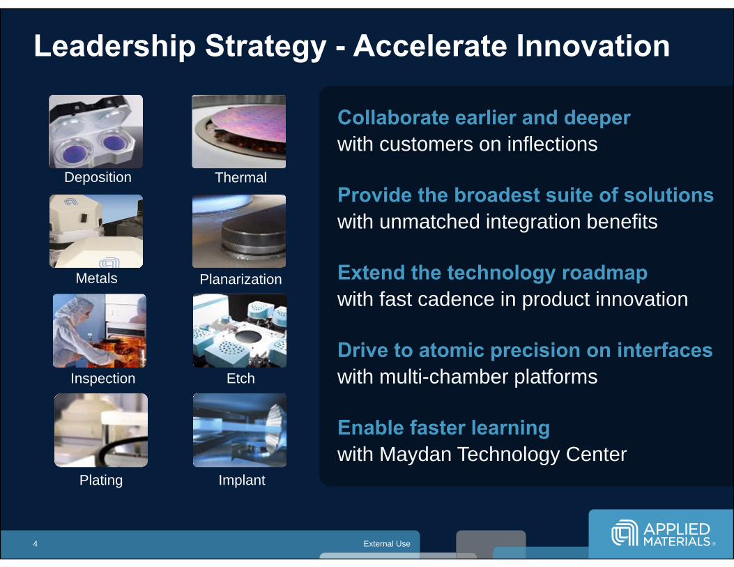
Leadership Strategy - Accelerate Innovation
4
Collaborate earlier and deeperwith customers on inflections
Provide the broadest suite of solutionswith unmatched integration benefits
Extend the technology roadmapwith fast cadence in product innovation
Drive to atomic precision on interfaces with multi-chamber platforms
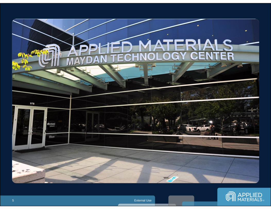
Enable faster learning with Maydan Technology Center
Plating
Thermal
Metals
Deposition
EtchInspection
Planarization
Implant
External Use5
External Use
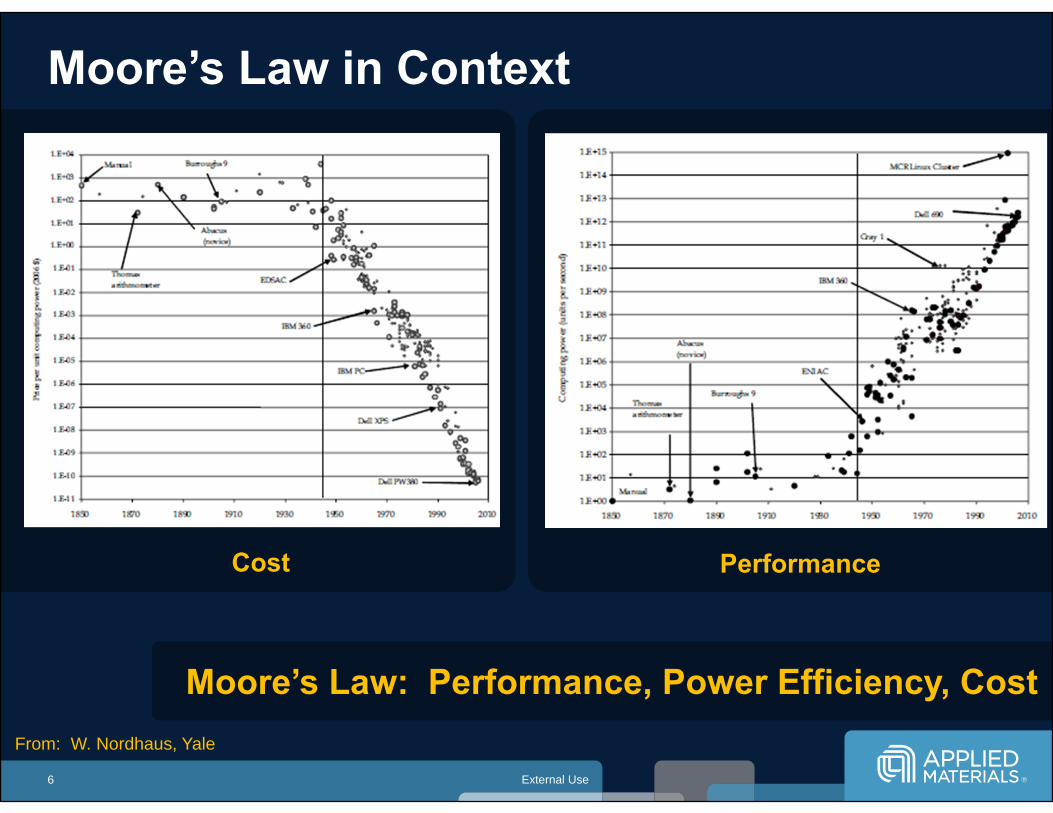
Moore’s Law in Context
6
Moore’s Law: Performance, Power Efficiency, CostFrom: W. Nordhaus, Yale
PerformanceCost
External Use
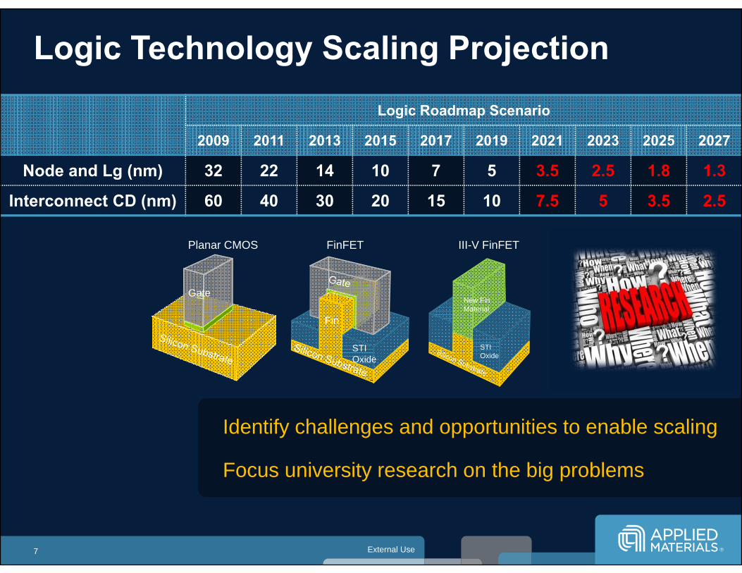
Logic Technology Scaling Projection
7
New FinMaterial
STI Oxide
Identify challenges and opportunities to enable scaling
Focus university research on the big problems
Logic Roadmap Scenario
2009 2011 2013 2015 2017 2019 2021 2023 2025 2027
Node and Lg (nm) 32 22 14 10 7 5 3.5 2.5 1.8 1.3
Interconnect CD (nm) 60 40 30 20 15 10 7.5 5 3.5 2.5
III-V FinFET
Gate
STI Oxide
Fin
Planar CMOS FinFET
External Use8
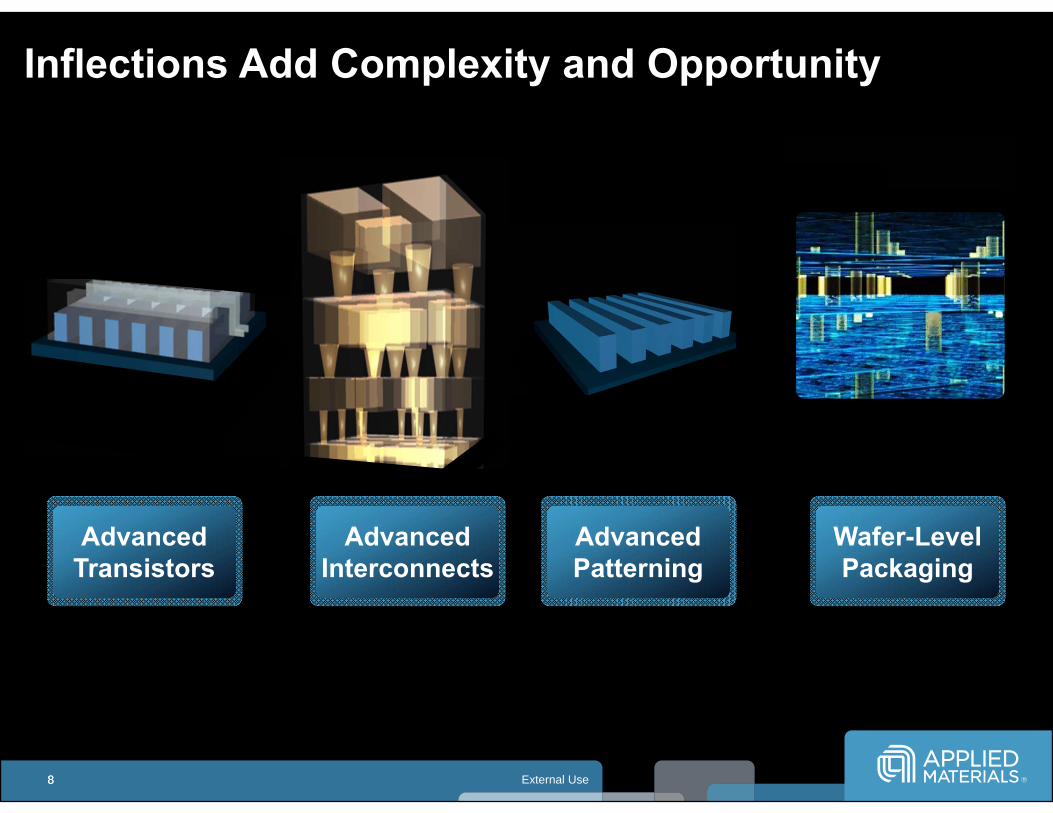
Inflections Add Complexity and Opportunity
8
Advanced Patterning
Advanced Interconnects
Wafer-Level Packaging
Advanced Transistors
External Use9
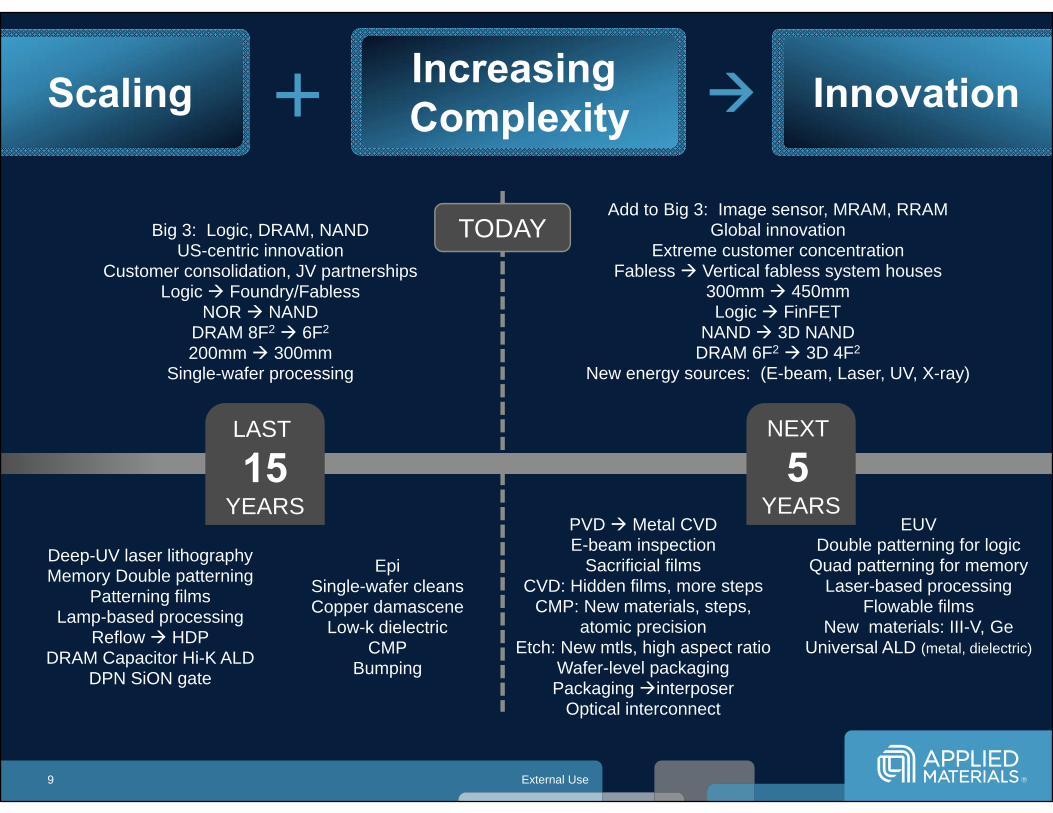
Scaling Increasing Complexity+
NEXT
5YEARS
LAST
15YEARS
TODAY
PVD Metal CVDE-beam inspection
Sacrificial filmsCVD: Hidden films, more steps
CMP: New materials, steps, atomic precision
Etch: New mtls, high aspect ratioWafer-level packagingPackaging interposer
Optical interconnect
Big 3: Logic, DRAM, NANDUS-centric innovation
Customer consolidation, JV partnershipsLogic Foundry/Fabless
NOR NANDDRAM 8F2 6F2
200mm 300mmSingle-wafer processing
Innovation
EpiSingle-wafer cleansCopper damascene
Low-k dielectricCMP
Bumping
Deep-UV laser lithography Memory Double patterning
Patterning filmsLamp-based processing
Reflow HDPDRAM Capacitor Hi-K ALD
DPN SiON gate
Add to Big 3: Image sensor, MRAM, RRAM Global innovation
Extreme customer concentrationFabless Vertical fabless system houses
300mm 450mmLogic FinFET
NAND 3D NANDDRAM 6F2 3D 4F2
New energy sources: (E-beam, Laser, UV, X-ray)
EUVDouble patterning for logic
Quad patterning for memoryLaser-based processing
Flowable filmsNew materials: III-V, Ge
Universal ALD (metal, dielectric)
External Use
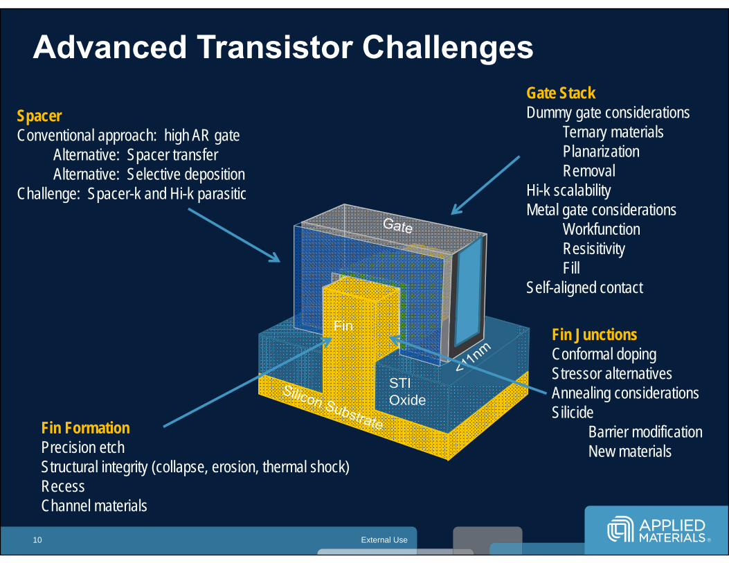
Advanced Transistor Challenges
10
STI Oxide
Fin
SpacerConventional approach: high AR gate
Alternative: Spacer transferAlternative: Selective deposition
Challenge: Spacer-k and Hi-k parasitic
Fin FormationPrecision etchStructural integrity (collapse, erosion, thermal shock)RecessChannel materials
Gate StackDummy gate considerations
Ternary materialsPlanarizationRemoval
Hi-k scalabilityMetal gate considerations
WorkfunctionResisitivityFill
Self-aligned contact
Fin JunctionsConformal dopingStressor alternativesAnnealing considerationsSilicide
Barrier modificationNew materials
External Use
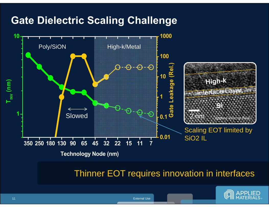
Gate Dielectric Scaling Challenge
11
350 250 180 130 90 65 45 32 22 15 11 7
1
10
T INV (n
m)
Technology Node (nm)
0.01
0.1
1
10
100
1000
Gat
e Le
akag
e (R
el.)
Poly/SiON High-k/Metal
Slowed
Thinner EOT requires innovation in interfaces
2 nm Applied Internal Data
Scaling EOT limited by SiO2 IL
External Use
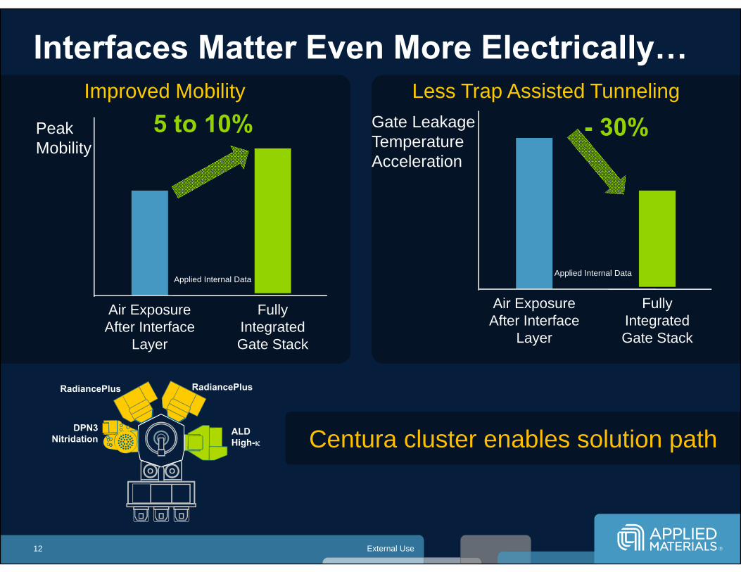
Interfaces Matter Even More Electrically…
Fully Integrated Gate Stack
Air Exposure After Interface
Layer
Improved Mobility
Peak Mobility
5 to 10%
Applied Internal Data
12
Less Trap Assisted Tunneling
Fully Integrated Gate Stack
Air Exposure After Interface
Layer
Gate Leakage Temperature Acceleration
- 30%
Applied Internal Data
ALDHigh-
RadiancePlus RadiancePlus
DPN3 Nitridation Centura cluster enables solution path
External Use
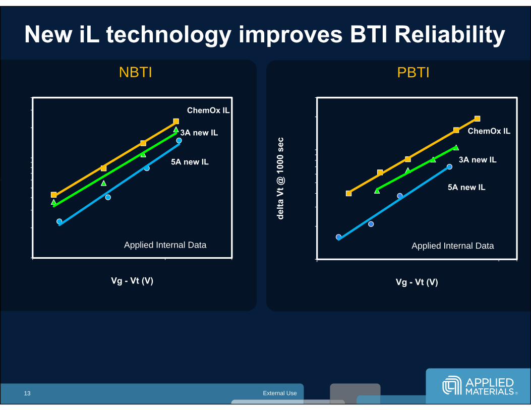
New iL technology improves BTI ReliabilityNBTI PBTI
0.01
0.1
0.7de
lta V
t @ 1
000
sec
Vg - Vt (V)
ChemOx IL
3A new IL
5A new IL
0.01
0.1
0.6
@
Vg - Vt (V)
ChemOx IL
3A new IL
5A new IL
Applied Internal Data Applied Internal Data
13
External Use
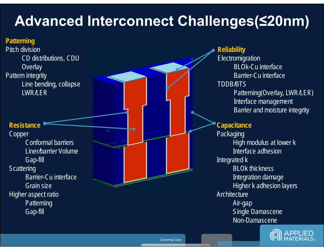
Advanced Interconnect Challenges(≤20nm)
ReliabilityElectromigration
BLOk-Cu interfaceBarrier-Cu interface
TDDB/BTSPatterning(Overlay, LWR/LER)Interface managementBarrier and moisture integrity
CapacitancePackaging
High modulus at lower kInterface adhesion
Integrated kBLOk thicknessIntegration damageHigher k adhesion layers
ArchitectureAir-gapSingle DamasceneNon-Damascene
ResistanceCopper
Conformal barriersLiner/barrier VolumeGap-fill
ScatteringBarrier-Cu interfaceGrain size
Higher aspect ratioPatterningGap-fill
PatterningPitch division
CD distributions, CDUOverlay
Pattern integrityLine bending, collapseLWR/LER
External Use
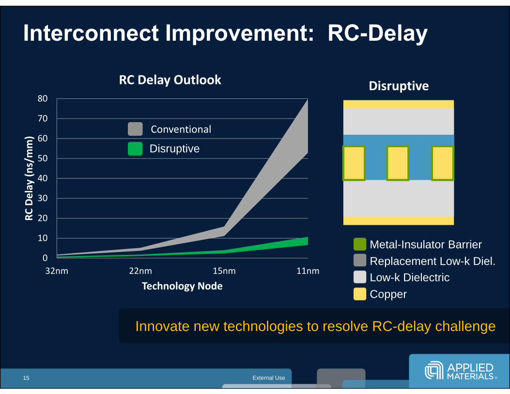
Interconnect Improvement: RC-Delay
15
Conventional
Disruptive
Disruptive
Metal-Insulator BarrierReplacement Low-k Diel.Low-k DielectricCopper
0
10
20
30
40
50
60
70
80
32nm 22nm 15nm 11nm
RC Delay (n
s/mm)
Technology Node
RC Delay Outlook
Innovate new technologies to resolve RC-delay challenge
External Use
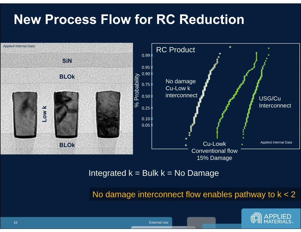
New Process Flow for RC Reduction
SiN
BLOk
BLOk
16
Low
k
Integrated k = Bulk k = No Damage
No damage interconnect flow enables pathway to k < 2
Applied Internal Data
0.050.10
0.25
0.50
0.75
0.900.95
0.99
-3
-2
-1
0
1
2
3
USG/CuInterconnect
No damageCu-Low k interconnect
Cu-LowkConventional flow
15% Damage
% P
roba
bilit
y
RC Product
Applied Internal Data
External Use
0.05
0.10
0.25
0.50
0.75
0.90
0.95
0.99
-3
-2
-1
0
1
2
3
1 10 100 1000 10000
17
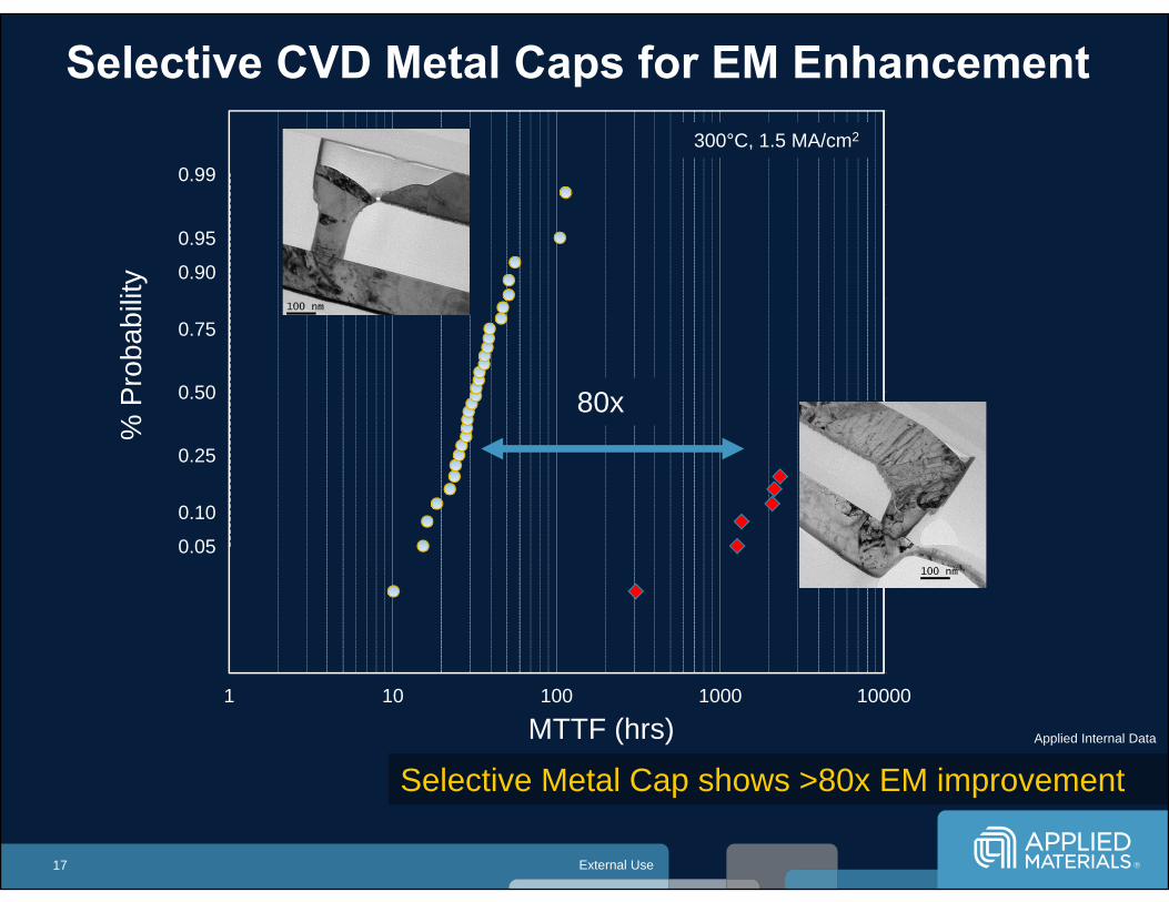
Selective CVD Metal Caps for EM Enhancement
Applied Internal Data
Selective Metal Cap shows >80x EM improvement
% P
roba
bilit
y
MTTF (hrs)
80x
300°C, 1.5 MA/cm2
External Use
Innovation to Advance Moore’s Law
18
Semiconductor Value Chain - Equipment
Moore’s Law Challenges
Core Technology Focus
Opportunities for Innovation
External Use
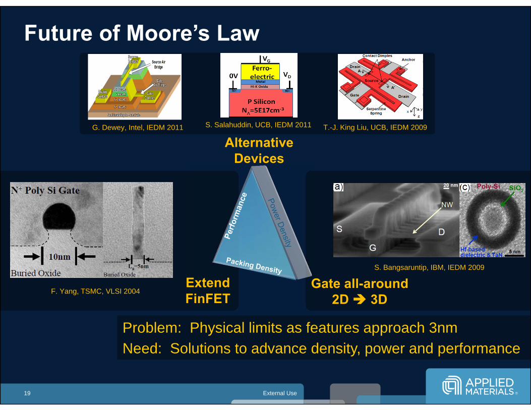
Future of Moore’s Law
19
Problem: Physical limits as features approach 3nmNeed: Solutions to advance density, power and performance
F. Yang, TSMC, VLSI 2004
S. Bangsaruntip, IBM, IEDM 2009
ExtendFinFET
Gate all-around2D 3D
Alternative Devices
G. Dewey, Intel, IEDM 2011 T.-J. King Liu, UCB, IEDM 2009S. Salahuddin, UCB, IEDM 2011
External Use
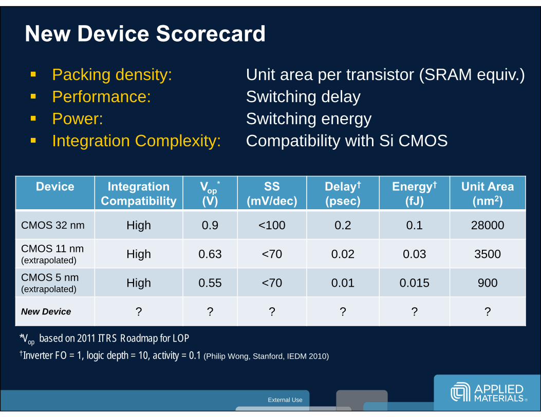
Packing density: Unit area per transistor (SRAM equiv.) Performance: Switching delay Power: Switching energy Integration Complexity: Compatibility with Si CMOS
Device IntegrationCompatibility
Vop*
(V)SS
(mV/dec)Delay†
(psec)Energy†
(fJ)Unit Area
(nm2)
CMOS 32 nm High 0.9 <100 0.2 0.1 28000
CMOS 11 nm(extrapolated) High 0.63 <70 0.02 0.03 3500
CMOS 5 nm (extrapolated) High 0.55 <70 0.01 0.015 900
New Device ? ? ? ? ? ?
*Vop based on 2011 ITRS Roadmap for LOP †Inverter FO = 1, logic depth = 10, activity = 0.1 (Philip Wong, Stanford, IEDM 2010)
New Device Scorecard
External Use
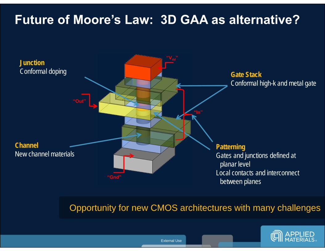
Junction Conformal doping Gate Stack
Conformal high-k and metal gate
ChannelNew channel materials
PatterningGates and junctions defined at
planar levelLocal contacts and interconnect
between planes“Gnd”
“Vdd”
“Out”
“In”
Future of Moore’s Law: 3D GAA as alternative?
Opportunity for new CMOS architectures with many challenges
External Use
Focus Areas for Research Core Technology
– Energy sources– Chemical delivery systems & chemistries– E-beam– Variability management
Materials– Screening methods– Alternative materials: Graphene, Metal Oxide, III-V, optical
Devices– 100mV switches– High packing density logic– Alternate channel, Optical interconnect, Interposer
EUV Lithography
22

Recommended