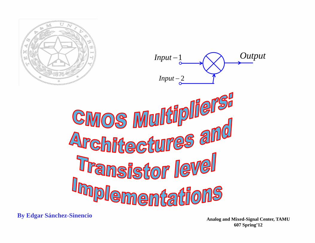
Analog and Mixed-Signal Center, TAMU607 Spring’12
1Input
2Input
Output
By Edgar Sánchez-Sinencio

multipliers.ppt
MultipliersWhat is a multiplier?
How do you obtain a multiplier?
.dimensionssuitableith constant w a isK andoutput theis Zsignals,input thearey and x
WhereKxyZ
x
y
Z
)t(v
)t(v)t(v
2
1
i)t(v)t(kvi 210
3i
2ii0
cv
bvavi
i.e.,Device
Nonlinear
scheme oncancellati
tyNonlineari
Fig. 1 Basic idea of multiplier

Transconductance-Mode Multiplier
1mG 1mG
1mG
2mG
1v 1v
1v
2v
1biasI1biasI
1biasI
2biasI2i 2i
0i 0i
122110 vkvvki
(a)(b)
(c)
1mG
2mG1v 2v 1biasI
2biasI
2i
1mG
1biasI
2110 vvki
1mG
2mG
1biasI
2biasI2i
1mG
2i
1biasI
2110 vvk2i
1v
2v
1v
(d) (e)
Fig. 2 Multiplication operation using programmable transconductor

How Does It Work?
)t(v)t(vk2)t(i2(e). . Figin dillustrate as inputs
aldifferentifully are vand vand ,uctor transcondaldifferentifully a becomes )(Guctor transcond third when theachieved ison cancellatiBetter . 2(d) . Fig
in shown as eliminated becan component This . )t(vk ,component unwantedan and , )t( vand )t( vsignals twooftion multiplica therepresents )t(i , Thus
)t(vk)t(v)t(vk)t(ior
V2
)t(vIV2V2
)t(v)t(vI)t(vV2
IV2
)t(v)t(vG)t(i
)t(vV2
)t(vGIvG)t(i
V2
IG
becomes G or,ansconductbipolar tr aFor )I(GG
where vGi
2110
21
m2
12
210
122110
t1bias1
tt212bias
1t1bias
t212m
0
1t
22m1bias11m0
t1bias
m1
m1
1bias1m1m
11m0
(1)
(2a)
(2b)
(3a)
(3b)
(3c)
(4)

Basic Multiplier Architectures
x
x-
y-
y
y
xy
xy
xy-
xy-
xy4
-
+
(a) using single-quadrant multipliers
yx
yx-
22 yxy2x
xy8
-
+
yx
yx
( )2
( )2
( )2
( )2
22 yxy2x
22 yxy2x 22 yxy2x
(b) using square divices
xy4)yY)(xX()yY)(xX(
)yY)(xX()yY)(xX(
xy8)}yY()xX{()}yY()xX{(
)}yY()xX{()}yY()xX{(
or
22
22
Where capital ( low case) letters represent DC (time domain) signals.

How the x and y Inputs can be Applied?
Consider a one transistor case first.
x
y
di
yx
di
x
y
di
di didi
diyx
xy
yxyx
(a) (b) (c) (d) (e) (f) (g)
Voltage signal injection methods
TgsdsTgs2TTgs
2gs
2Tgsd
TgsdsTgs
2ds
dsTdsgsdsds
Tgsd
VVV , VVfor VVV2V2KVV
2KI
VVV , VVfor 2
VVVVVKV
2VVVKI
:asexpressedismodelr transistoMOSsimple The
Results are summarized next.
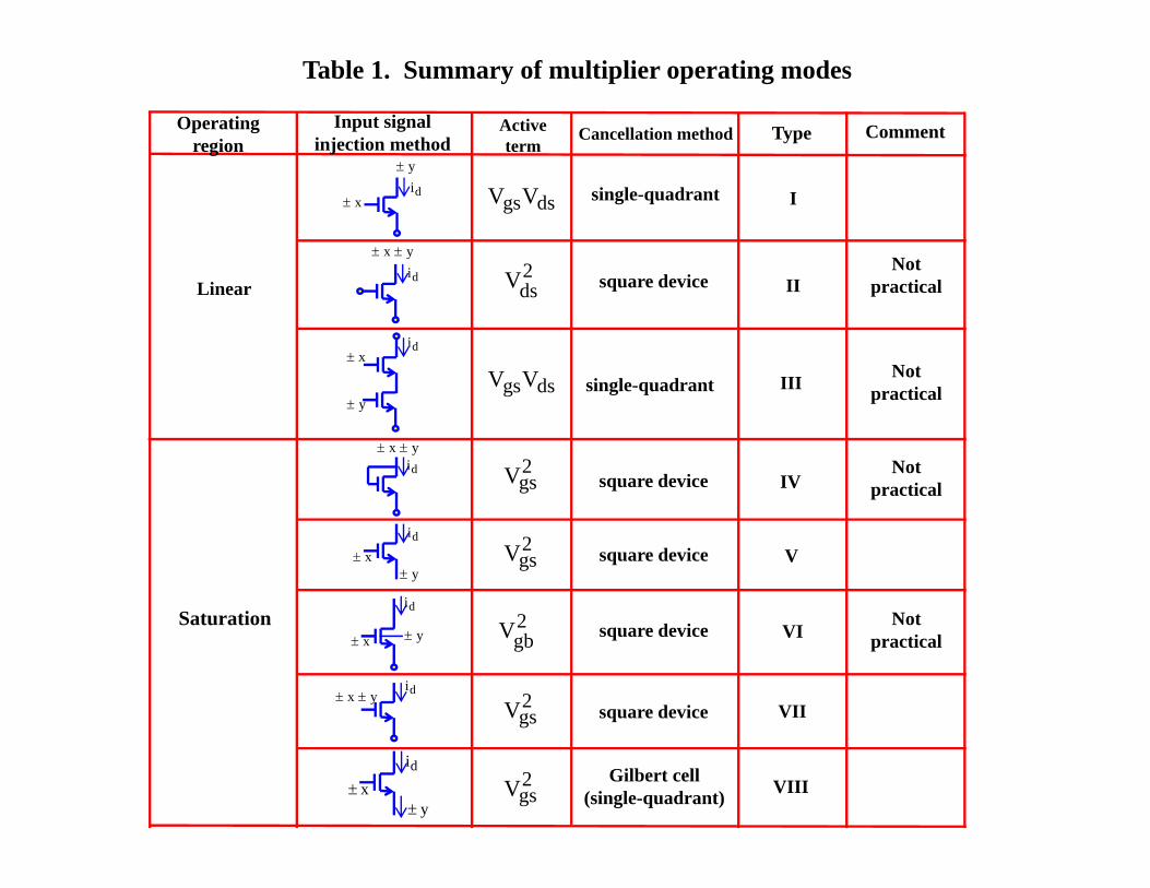
Table 1. Summary of multiplier operating modes
x
y
di
yx
di
x
y
di
di
di
di
di
yx
xy
yx
yx
di
xy
Operatingregion
Input signalinjection method
Linear
Saturation
Activeterm
Cancellation method Type Comment
single-quadrant
single-quadrant
square device
square device
square device
square device
square device
Gilbert cell(single-quadrant)
I
II
III
IV
V
VI
VII
VIII
Notpractical
Notpractical
Notpractical
Notpractical
dsgsVV
2dsV
dsgsVV
2gsV
2gsV
2gbV
2gsV
2gsV
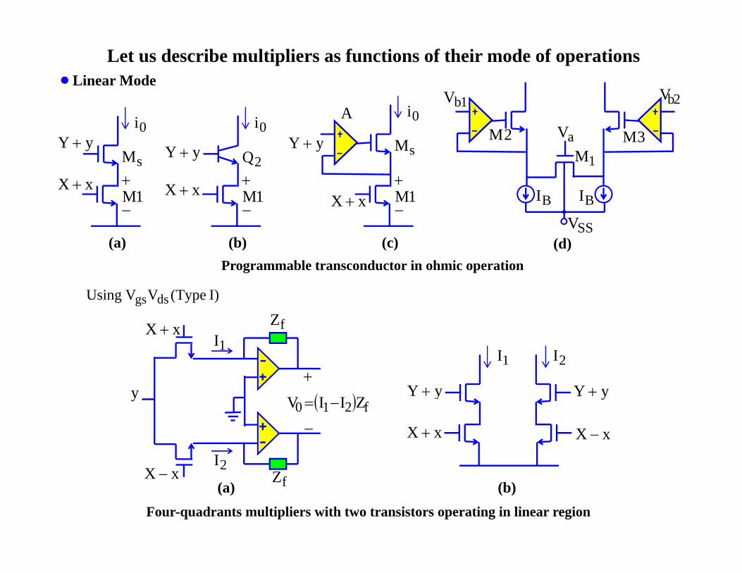
Let us describe multipliers as functions of their mode of operationsLinear Mode
yY
xX
0i
(a)
sM
1M
yY
xX
0i
(b)
2Q
1M
yY
xX
0i
(c)
sM
1M
A
(d)
BI BI
1MaV2M 3M
1bV 2bV
SSV
Programmable transconductor in ohmic operation
I) Type(VV Using dsgs
xX
xX
y
1I
2I
fZ
fZ
f210 ZIIV
(a)
yY
xX xX
yY
1I 2I
(b)Four-quadrants multipliers with two transistors operating in linear region

Multiplier Implementations Using VgsVds (Type I)
1I
2I
3I
4I
yY
xX
yY
xX
xX
01I02I
fZ
0V
yY
xX
yY
xX
xX
01I
02ISM
bV1fR 2fR
ddV
0V
0V
7(a) 7(b)
01I 02I
yY
xX SM
1M 1M
yY
xX
1I2I 3I
4I
xX
Fig. 7 Fully-differential four-quadrant multipliers using VgsVds term (Type I)7(c)
xX xX
yY 1MSM SM
1M
yY yY
01I 02I
7(d)
3V3V
3M 5M 4M
1DA 3DA 2DA3DI 4DIDDV
T2143
SSV)V,Vmin()V,Vmax(
V
1BI 3BI 2BI
1V 2V1M 2M1DI 2DI
7(e)
4V

Example of a Complete Implementation of Multiplier VgsVds Type I.{From Fig. 7(e)}
gy technolom2tagessupply vol V3
1M 2M
3M
4M5M6M 7M8M 9M10M
11M12M
13M
14M15M
1MB2MB
3MB
SSV
DDV
K1 K1
1V 2V3V
4V
3DI 4DI
2M1M 5M3M 10M6M 15M11M 3MB1MB Transistors
mL/mW 50/10 5/100 10/10 5/50 10/10
(3) VVVVK2IIIII : as written becan then Icurrent output The .III and KKKlet Now,
VV and VV Thus voltages.source anddrain same thehave M2 and M1at evident th isIt
(2) V21VVVK2IIII
and
(1) V21VVVK2IIII
43212D1D4D3Dout
outB2BB121
2TT12DSDS1
22DS2DS2T2GS22B2D2B4D
21DS1DS1T1GS11B1D1B3D
8V

Low voltage multiplier working with transistors in linear region. (Coban & Allen)
461
21110
DS111ba
K/KKK with
uctors. transcondfollowing theof tworequires vKv'III VvKI range.linear in M1 and M1
supply 1.5V single One
1:1in outDDV DDV
aI bI
1BV1BV
a1M b1M
a2Ma3M
a4M
a5M a6Mb2M
b4M
b3M
b5Mb6M
2vVV 2
2C2B
1DSV
1DSV
SSV2vV 1
1C 2vV 1
1C
circuit. cascode regulated on the Based r.transistocomposite Use
rs.transistosingle asdrawn rstransistocompositeth circuit wi complete The
DDV
SSV
1M 2M '1M '2M
aM bM 'Ma'Mb 2vV 1
1C 2vV 1
1C
2vV 2
2C 2
vV 22C
2BV 2BV
1I 'I1outI
Low voltage transconductor block
Proposed low voltage four quadrant multiplier
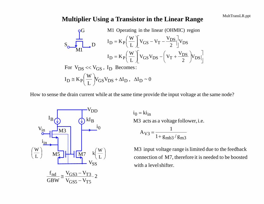
Multiplier Using a Transistor in the Linear RangeG
S D1M
DSDS
TDSGSPD
DSDS
TGSPD
V2
VVVVLWKI
V2
VVVLWKI
region(OHMIC)linear in theOperating 1M
0~I , IVVLWKI
:Becomes I , VVFor
DDDSGSPD
DGSDS
node?sameat theageinput volt theprovidetimesameat theilecurrent whdrain thesense toHow
DDV
SSV
inV
BI BkI0i3M
5M 7M
ini
LWk
LW
2VVVV
GBWf
5T5GS3T3GSnd
3m3mbV3
in0
g/g11A
i.e. follower, voltagea as acts 3Mkii
shifter. levelawith boosted be toneeded isit thereforeM7, of connection
feedbackthetoduelimitedisrangeageinput volt 3M
MultTransLR.ppt

A possible implementation follows:
BI BkI3D
3M
5M
inv0i
MR
mnI
7M
3D
LSRLSC
Version 1 of a complete multiplier (mixer)
1M
2M 3M
4M 5M 7M
8M 9M
11M11M
12M 13M14M 15M
1CS2CS4CS 3CS
6CS 5CSLFCLFC
OUT OUT
BB BB
LO
LSC LSCLSR LSR
REFV REFV
The differential linear up-conversion mixer; the single ended carrier signal is applied at the LO terminal and the differential baseband signal is appliedat the BB terminals. The baseband modulation feedthrough in the output signal is suppressed through the output circuits (thin lines) which act as active coils

Version 2: Multiplier Using Cascode Current Source.
DDV
SSV
1M5M4M 7M6M
MR MR
2M 3M
8M 9M10M 11M
12M 13M 14M 15MCMV
mpV
mnV
1BI 1BI 2BI2BI
BI BI
1DI0I0I ib
2/Vi2/Vi
MbMb
Switching Modulator Based on Linear MOS
2VbV
)L/W()L/W()L/W(KI
2VbV
)L/W()L/W()L/W(KI
then, CM asact M7 , M5 and M6 , M4
)L/W(KI :yieldsit , I Neglecting
V2V
2VV
2/V- V and 2/VVfor Thus
)L/W(KIVVV
)L/W(KIVVV
M3M2For
iii
57
1p0
iii
46
1p0
1pD1
D
iii
1DS
i-1i1
3p1B
0T1D1
2p1B
0T1S1
iiii
5,4
7,6
1pd0
2iii
5,4
7,6
1p
00d0
bVfor bV)L/W()L/W(
LWKI
VbV2)L/W()L/W(
LWK
2III

Linear Operation using V2ds (Type II)
01I 02I
xX xX
yY yYSM
1MDDV
Fig. 8 Multiplier using V2ds (Type II)
KxyIII 02010
x
y
xy
A possible summer implementation

Dual Gate in Linear Range (Type III)
yx,C and VVVVC and
IIfor KI
V WhereRegion.Linear in M2& M1
region saturationin MM
polTScom
poldd
polpol
2d1d
dI polI
2dM 1dM
1M
2MpolV
SV
bI
xVcom
yVcom
xVcom
xVcomyVcom yVcom
polI
bI
01I 02I
9(a) 9(b)Fig. 9 Four quadrant multiplier using dual gate (Type III)
xyc
KVI
))yx(c4)()yx(c4(c2yxcxyKV8III
pol0
2222
222pol02010

MOS Multipliers Operation in Saturation Region
01I 02I
xX xX
yY yY
Kxy4III rearchitectu4xy on the Based
V) (Type term.V using
multiplierFETs coupled crossFour
02010
2gs
01I 02I
xX xX
yY yYSM
1M
SM
IV) (Type connection diode with V using Multiplier 10 Fig. 2gs

Alternative Signal Injection Implementations using V2GS
01I 02I
xX
xX
yY
RR
Y
yY yY
xX xX
01I 02I
SSV
12(a) Using OP Amp 12(b) Using a linear differential amp
xX
yY SM
1M 1M
01I 02I
xX
yY
ddVddV
SM
02I01I
ddVxX
SM SM SM SM
yY xX yY
12(c) Using source followers 12(d) A separate follower for each cross-coupled transistor
Fig. 12 Source signal injection methods for multiplier using V2gs term (Type V)

Bulk-Driven Transistor Using V2gs (Type VI)
yY yY
01I 02I
xX S
xX
ysY2for xysY2
K4I
xsY22
ysY2ysY2
K4III
2V2VV
FF
0
3
FF
F01020
FbsF0TT
Fig. 13 Using substate signal injection (Type VI)

Voltage Adder (Type VII) using V2gs
01I 02I
xX xX
yY yY
01I 02I
xX xX
yY yY
GND
14(a) with tail current 14(b) without the tail current
Fig. 14 Multipliers using voltage adder (Type VII)
adders. active (iii)or ,capacitors (ii) resistors, (i) with dimplemente becan Summers scheme.on cancellati ) ( on the based istion implementa This 2

Floating Voltage Source (Type VII) Using V2gs
01I 02I
yY
xX
Fig. 15 Multiplier using floating voltage source (Type VII)

MOS Gilbert Cell (Type VIII)Analysis:
signalcurrent a is )y(I and signal voltagea is x followsIn what
IKx1xKI2III yieldspair aldifferenti MOS One
y
21
s
2s02010d
01I 02I
xX
xX
1yI2yI
Current steering circuit
signals. voltagearey andboth x HereKK2xy2III
Thus
K2yII
Thus next.shown
aspair aldifferenti thirdaby generated is II that Note
IIxK2III
:obtainwepairs,aldifferenti twoFor the
302010
32y1y
2y1y
2y1y02010

01I 02I
xX
xX
1yI 2yI
01I 02I
xX
xX
MOS Gilbert Multiplier Implementations
yY yY 3M
SI
1yI 2yIyY yY
GND
17(a) with tail current 17(b) without tail current
Fig. 17 MOS Gilbert multipliers (Type VIII)
supplies.power lowfor suitable benot might structure This s.attenuator activeor resarchitectu folded pairs,
aldifferentitheofion linearizatinvolvecellthisoft Improvemen

Comparisons
next. discussed are simulationthrough andequalitativlimitedA dependent.n applicatioiscomparison specificA
Table 2. Summary of general qualitative comparison of 15 multiplier topologies.
NO. Type Circuit Diagram Figure Worse than Remark
1
2
3
4
5
6
78
I
I
II,III,IV
V
V
VI
VII
VIII
7(a), 7(b)
7(c),7(d)
8, 9, 10
12(a)
12(b), (c), (d)
13
14, 15
17
2
2
2
5
5
5
Require additional circuitry.
Require additional circuitry.
Require additional circuitry.Poor linearity.
Require OP Amp
Poor linearity
High power supply voltage.Poor linearity.

0
0.5
1
1.5
2
2.5
0.5 1 1.5 2
2y[volt]
THD
[%]
fig.8(C)fig. 8(d)fig. 13(b)fig. 13(c)fig.13(d)
0
0.5
1
1.5
2
2.5
0.5 1 1.5 2
2x[volt]
THD
[%]
fig. 7(C)fig. 7(d)fig. 12(b)fig. 12(c)fig. 12(d)
Simulated Total Harmonic Distortion(THD) for W/L= 10m/10m for all transistors.
0.00
0.05
0.10
0.15
1 2 3
W/L ratio of source follower
THD[
%]
fig. 7(c)fig. 12(c)fig. 7(c)fig. 12(c)2y = 0.5V
2x = 0.5Vp-p
2x = 0.5V2y = 0.5Vp-p
Effect of source follower's W/L ratio on THD
THD Comparisons

Linearity Comparison
0 10
0.5
1
1.5x 10⁻⁵
0 1-20
-15
-10
-5
0
0 10
0.5
1
1.5x 10⁻⁵
0 0.5 1-20
-10
0
10
20
Iout[A]
Iout[A]
y [V] y [V]
x [V] x [V]
x = 1V
y = 1V
Fig. 7(d)Fig. 7(c)Fig. 12(c)
Linearityerror[%]
Linearityerror[%]
(a) Output current for fixed x (b) Linearity error for fixed x
x = 1V
y = 1V
0.5
0.5 0.5Fig. 7(d)
Fig. 7(c)
Fig. 12(c)
Fig. 7(d)Fig. 7(c)Fig. 12(c)
Fig. 7(d)
Fig. 7(c)
Fig. 12(c)
(a) Output current for fixed y (b) Linearity error for fixed y
Measurement results for W/Lm1 = 5µm/17µm and W/Lsource follower = 50µm/10µm.
y. technologCMOS m22Vy x,n,consumptioW 360 ,V/A10gm

Input Range and Minimum Power Supply
dV
yY
xX
saturation
linear
1V
saturation
dV
yY xX
ddV
current Tail1V
(a) Circuit Fig. 7(c) (b) Circuit Fig. 12(c)
Fig. 24 Bias conditions
dT
T
TT1
T
VVyYyYV
VxXVyYVxXV
:7(c) Fig. For
DDV
DV
0V
TVDDV
0V
DVTV
TV
y2
y2x2
x2
X
X
Y
Y
TV
tail;dssatVGND
(a) Circuit Fig. 7(c) (b) Circuit Fig. 12(c)
Fig. 25 Input range and power supply voltage
DT
T1
T1 tailsat; ds
VVxXxXyYVV
VyYVV12(c)Fig.For

Table 3. Summary of a comparative multiplier study for equal size transistors.
Table 4. Summary of comparison between circuit Fig. 7(c), Fig. 7(d), and Fig. 12(c)
CircuitMax Gm[µA/V]
PowerConsumption[mW]
MismatchSensitivity
Linearityx
Linearityy
Fig. 7(c)Fig. 7(d)Fig. 12(b)Fig. 12(c)Fig. 12(d)
204.65
4025
238270200295480
Good
Good
GoodGoodGoodBadBadBad
BadBadBadWorst
Worst WorstBest Best
Circuit Linearity Minimum PowerSupply
Noise
Good
Good
Bad Bad
Bad
Bad
Bad
Good GoodFig. 7(c)
Fig. 7(d)
Fig. 12(c)

outp
ut n
oise
[nV
2 ]
(W/L)1
1 5 9910
915
920
925
(W/L)2=10
(W/L)2=20
inpu
t noi
se [m
V2 ]
(W/L)1
1 5 92
4
6
8
10
(W/L)2=20
(W/L)2=10
Noise Consideration for Fig. 7(c).
(a) (b)
Fig. 26 Noise dependency on (W/L)1 for (X+Y)/2 = 4 volt and X-Y = 2 volt.
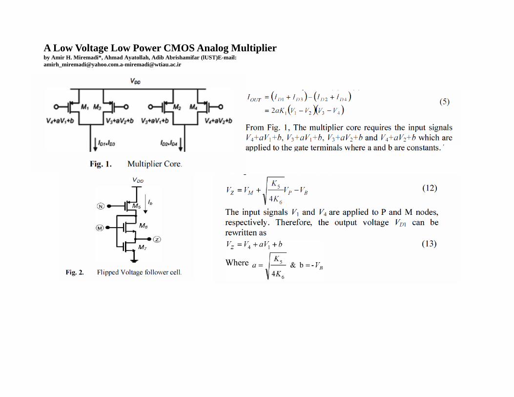
A Low Voltage Low Power CMOS Analog Multiplier by Amir H. Miremadi*, Ahmad Ayatollah, Adib Abrishamifar (lUST)E-mail: [email protected]@wtiau.ac.ir


VRF
VLO
S1
RL
VIF VRF
RL
VIF
VLO
M1
Simple switch used as a mixer
Implementation of switch with an NMOS device
MIXERS

R1
M2
R2
M3
VDD
VLO
VLO M1
VIF
Active Mixer

Vin
RLS
+
-LO LO
IF
SignalBand
ImageBand
ThermalNoise
Spectrum at X
Spectrum at Y
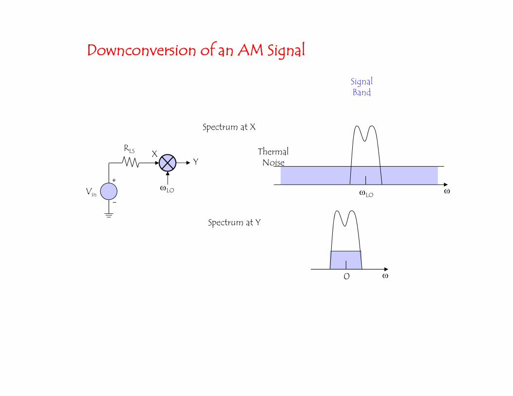
Folding RF and image noise into the IF band
XY
Vin
RLS
+
-LO LO
0
SignalBand
ThermalNoise
Spectrum at X
Spectrum at Y
Downconversion of an AM Signal
XY

R1
M2
R2
M3
VDD
VLO
VLO M1
VIF
Single-balanced mixer Double-balanced mixer
R1 R2
M4
VDD
VLO
VLO M1
VIF
M3
M5 M6
RD
M2
RD
M3
VDD
VLO
VbM1
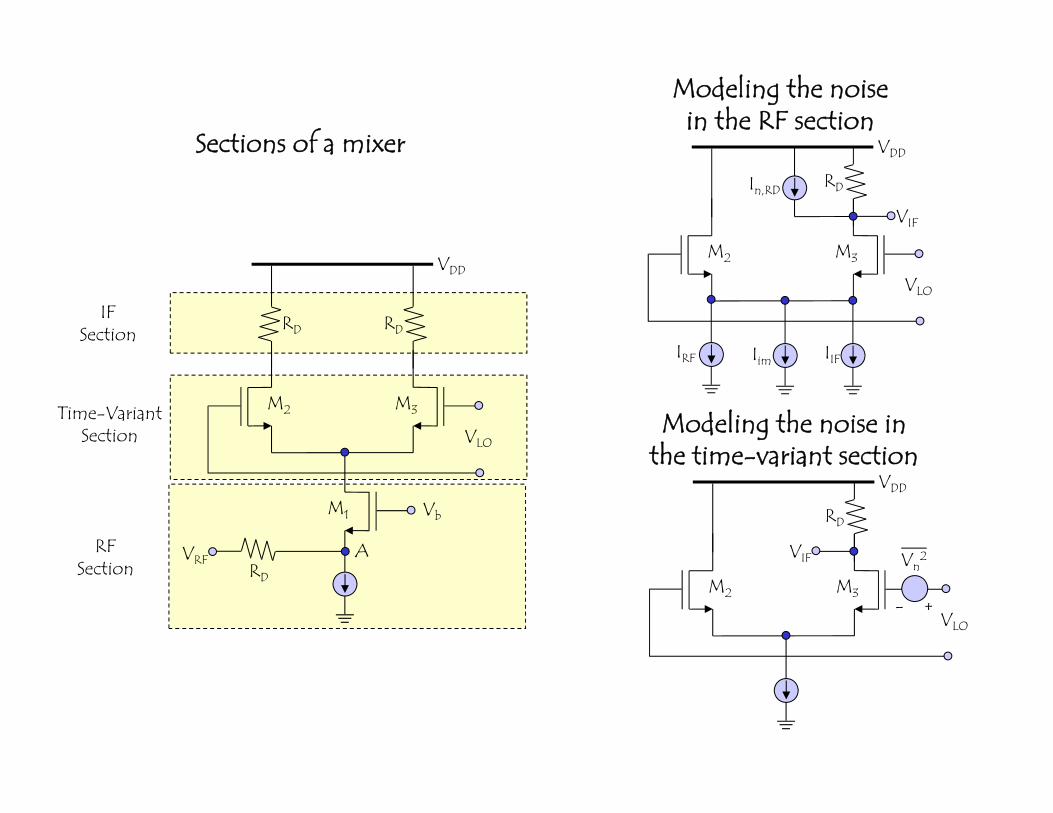
Sections of a mixer
RD
AVRF
IFSection
Time-VariantSection
RFSection
M2
RD
M3
VDD
VLO
Modeling the noise in the RF section
In,RD
VIF
IRF Iim IIF
M2
RD
M3
VDD
VLO
Modeling the noise in the time-variant section
VIF
- +
Vn2

Simple mixer with differential outputs
R R
VCC
Vout
IRF
-1
+1
IRFx
t
Simple mixer with single-ended output
R R
VCC
Vout
IRF
+1
IRFx
t
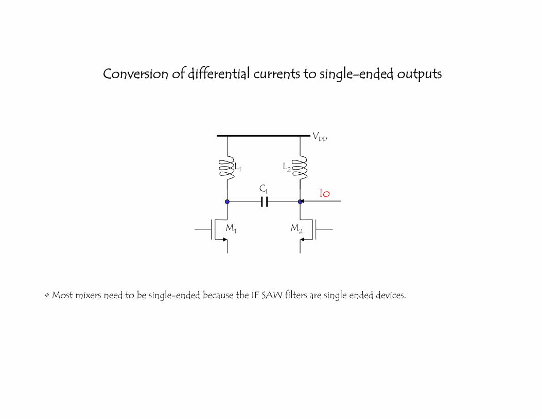
L1
M1
L2
M2
VDD
C1
Conversion of differential currents to single-ended outputs
• Most mixers need to be single-ended because the IF SAW filters are single ended devices.
Io

References
[1] G. Han and E. Sánchez-Sinencio, “CMOS Transconductance Multipliers: A Tutorial”, IEEE Trans.on Circuits and Systems II, vol. 45, No. 12, pp. 1550-1563, December 1998.
[2] F.N. Trofimenkoff and R.E. Smallwood, “Four Quadrant JFET Multipliers”, IEEE J. Solid-State Circuits, pp. 316-319, June 1977.
[3] Z. Czarnul and S. Takagi, “Design of Linerar Tunable CMOS Differential Transconductor Cells”,Elctron. Lett., vol. 26, pp. 1809-1811, 1992.
[4] Z. Czarnul, “Modification of Banu-Tsividis Continuous-Time Integrator Structure”, IEEE Trans. onCircuits and Systems, vol. CAS-33, No. 7, pp. 714-716, July 1986.
[5] J-H Tsag et al, “CMOS Four-Quadrant Multiplier Using Triode Transistors Based on Regulated Cascode Structure”, Electron Lett., vol. 31, pp. 962-963, June 1995.
[6] B. Razavi, “RF Microelectronics”, Prentice Hall, 1998.

Zhuo Zou, Mendoza, D.S., Peng Wang, Qin Zhou, Jia Mao, Jonsson, F., Tenhunen, H., Li-Rong Zheng, "A Low-Power and Flexible Energy Detection IR-UWB Receiver for RFID and Wireless Sensor Networks", Circuits and Systems I: Regular Papers, IEEE Transactions on, On page(s): 1470 - 1482 Volume: 58, Issue: 7, July 2011 2. Weiwei Shan, Yuan Ma, Newcomb, R.W., Dongming Jin, "Analog Circuit Implementation of a Variable Universe Adaptive Fuzzy Logic Controller", Circuits and Systems II: Express Briefs, IEEE Transactions on, On page(s): 976 - 980 Volume: 55, Issue: 10, Oct. 2008 3. Sigit Yuwono, Sok-Kyun Han, Sang-Gug Lee, "A 900-mV Area-Efficient Source-Degenerated CMOS Four-Quadrant Multiplier with 10.6-GHz Bandwidth", Wireless Communications, Networking and Mobile Computing, 2009. WiCom '09. 5th International Conference on, On page(s): 1 - 4 4. Mokarram, M., Khoei, A., Hadidi, Kh., Gheysari, K., "Implementation of centroid defuzzifier block using CMOS circuits", Intelligent Systems, 2008. IS '08. 4th International IEEE Conference, On page(s): 2-26 - 2-29 Volume: 1, 6-8 Sept. 2008 5. Wei Wu, Xiaoya Fan, Tingcun Wei, Charlesy, C.T., "A low-voltage low-power self-mixer for 3.1#x2013;5GHz non-coherent UWB receiver", Electron Devices and Solid-State Circuits, 2009. EDSSC 2009. IEEE International Conference of, On page(s): 24 - 27 6. Mahmoud, S.A., "CMOS fully differential CMOS Four-quadrant analog multiplier", Microelectronics, 2008. ICM 2008. International Conference on, On page(s): 27 - 30 7. Dei, M., Nizza, N., Bruschi, P., Piotto, M., "A four quadrant CMOS analog multiplier based on the non ideal MOSFET I–V characteristics", Research in Microelectronics and Electronics, 2008. PRIME 2008. Ph.D., On page(s): 33 - 36 8. Oliveira, V.J.S., Oki, N., "Low voltage four-quadrant current multiplier: An improved topology for n-well CMOS process", Design & Technology of Integrated Systems in Nanoscale Era, 2007. DTIS. International Conference on, On page(s): 52 - 55 9. Diwakar, K., Senthilpari, C., Singh, A.K., Soong, L.W., "Analog Multiplier with High Accuracy", Computational Intelligence, Communication Systems and Networks, 2009. CICSYN '09. First International Conference on, On page(s): 62 - 66 10. Lehne, M., Raman, S., "A 0.13- 1-GS/s CMOS Discrete-Time FFT Processor for Ultra-Wideband OFDM Wireless Receivers", Microwave Theory and Techniques, IEEE Transactions on, On page(s): 1639 - 1650 Volume: 59, Issue: 6, June 2011
Recent References on Multipliers
Recommended