IEEE 802.3af/at-Compliant, Powered Device Interface Controllers with Integrated Power MOSFET
MAX5969A/MAX5969B
EVALUATION KIT AVAILABLE
General DescriptionThe MAX5969A/MAX5969B provide a complete interface for a powered device (PD) to comply with the IEEE® 802.3af/at standard in a power-over-Ethernet (PoE) system. The MAX5969A/MAX5969B provide the PD with a detection signature, classification signature, and an integrated isolation power switch with inrush current control. During the inrush period, the MAX5969A/MAX5969B limit the current to less than 180mA before switching to the higher current limit (720mA to 880mA) when the isolation power MOSFET is fully enhanced. The devices feature an input UVLO with wide hysteresis and long deglitch time to compensate for twisted-pair cable resistive drop and to assure glitch-free transition during power-on/-off conditions. The MAX5969A/MAX5969B can withstand up to 100V at the input.
The MAX5969A/MAX5969B support a 2-event classifica-tion method as specified in the IEEE 802.3at standard and provide a signal to indicate when probed by Type 2 power-sourcing equipment (PSE). The devices detect the presence of a wall adapter power-source connection and allow a smooth switchover from the PoE power source to the wall power adapter.
The MAX5969A/MAX5969B also provide a power-good (PG) signal, two-step current limit and foldback, overtemperature protection, and di/dt limit.
The MAX5969A/MAX5969B are available in a space-saving, 10-pin, 3mm x 3mm, TDFN power package. These devices are rated over the -40NC to +85NC extended temperature range.
ApplicationsIEEE 802.3af/at Powered Devices
IP Phones, Wireless Access Nodes, IP Security Cameras
WiMAX® Base Station
FeaturesS IEEE 802.3af/at CompliantS 2-Event ClassificationS Simplified Wall Adapter InterfaceS PoE Classification 0 to 5S 100V Input Absolute Maximum RatingS Inrush Current Limit of 180mA MaximumS Current Limit During Normal Operation Between
720mA and 880mAS Current Limit and FoldbackS Legacy UVLO at 36V (MAX5969A)S IEEE 802.3af/at-Compliant, 40V UVLO (MAX5969B)S Overtemperature ProtectionS Thermally Enhanced, 3mm x 3mm, 10-Pin TDFN
19-5008; Rev 1; 7/15
+Denotes a lead(Pb)-free/RoHS-compliant package.*EP = Exposed pad.
Ordering Information
Pin Configuration
IEEE is a registered service mark of the Institute of Electrical and Electronics Engineers, Inc.
WiMAX is a registered certification mark and registered service mark of the WiMAX Forum.
PART TEMP RANGEPIN-
PACKAGE
UVLO THRESHOLD
(V)
MAX5969AETB+ -40NC to +85NC 10 TDFN-EP* 35.4
MAX5969BETB+ -40NC to +85NC 10 TDFN-EP* 38.6
1
3
4
10
8
7
CLS
PG
WAD
VDD
N.C.
I.C.
EP*
*EP = EXPOSED PAD. CONNECT TO VSS.
MAX5969AMAX5969B
2 9 2ECDET
5 6 RTNVSS
TDFN(3mm × 3mm)
TOP VIEW
+
For pricing, delivery, and ordering information, please contact Maxim Direct at 1-888-629-4642, or visit Maxim’s website at www.maximintegrated.com.

2 Maxim Integrated
IEEE 802.3af/at-Compliant, Powered Device Interface Controllers with Integrated Power MOSFET
MAX5969A/MAX5969B
Stresses beyond those listed under “Absolute Maximum Ratings” may cause permanent damage to the device. These are stress ratings only, and functional operation of the device at these or any other conditions beyond those indicated in the operational sections of the specifications is not implied. Exposure to absolute maximum rating conditions for extended periods may affect device reliability.
VDD to VSS ..........................................................-0.3V to +100VDET, RTN, WAD, PG, 2EC to VSS .......................-0.3V to +100VCLS to VSS ..............................................................-0.3V to +6VMaximum Current on CLS (100ms maximum) .................100mAContinuous Power Dissipation (TA = +70NC) (Note 1) 10-Pin TDFN (derate 24.4mW/NC above +70NC) Multilayer Board ........................................................1951mW
Operating Temperature Range .......................... -40NC to +85NCMaximum Junction Temperature .....................................+150NCStorage Temperature Range ............................ -65NC to +150NCSoldering Temperature (reflow) .................................... +260NC
ELECTRICAL CHARACTERISTICS(VIN = (VDD - VSS) = 48V, RDET = 24.9kω, RCLS = 619ω. RTN, WAD, PG, and 2EC unconnected, all voltages are referenced to VSS, unless otherwise noted. TA = TJ = -40NC to +85NC, unless otherwise noted. Typical values are at TA = +25NC.) (Note 3)
ABSOLUTE MAXIMUM RATINGS
PACKAGE THERMAL CHARACTERISTICS (Note 2)Junction-to-Ambient Thermal Resistance (θJA) .................. 4NC/WJunction-to-Case Thermal Resistance (θJC) ....................... 9NC/W
Note 1: Maximum power dissipation is obtained using JEDEC JESD51-5 and JESD51-7 specifications.Note 2: Package thermal resistances were obtained using the method described in JEDEC specification JESD51-7, using a four-
layer board. For detailed information on package thermal considerations, refer to www.maximintegrated.com/thermal-tutorial.
PARAMETER SYMBOL CONDITIONS MIN TYP MAX UNITS
DETECTION MODE
Input Offset Current IOFFSET VIN = 1.4V to 10.1V (Note 4) 10 FA
Effective Differential Input Resistance
dRVIN = 1.4V up to 10.1V with 1V step, VDD = RTN = WAD = PG = 2EC (Note 5)
23.95 25.00 25.5 kI
CLASSIFICATION MODE
Classification Disable Threshold
VTH,CLS VIN rising (Note 6) 22.0 22.8 23.6 V
Classification Stability Time 0.2 ms
Classification Current ICLASS
VIN = 12.5V to 20.5V, VDD = RTN = WAD = PG = 2EC
Class 0, RCLS = 619I 0 3.96
mA
Class 1, RCLS = 117I 9.12 11.88
Class 2, RCLS = 66.5I 17.2 19.8
Class 3, RCLS = 43.7I 26.3 29.7
Class 4, RCLS = 30.9I 36.4 43.6
Class 5, RCLS = 21.3I 52.7 63.3
TYPE 2 (802.3at) CLASSIFICATION MODE
Mark Event Threshold VTHM VIN falling 10.1 10.7 11.6 V
Hysteresis on Mark Event Threshold
0.84 V
Mark Event Current IMARKVIN falling to enter mark event, 5.2V P VIN P 10.1V
0.25 0.85 mA

3Maxim Integrated
IEEE 802.3af/at-Compliant, Powered Device Interface Controllers with Integrated Power MOSFET
MAX5969A/MAX5969B
ELECTRICAL CHARACTERISTICS (continued)(VIN = (VDD - VSS) = 48V, RDET = 24.9kω, RCLS = 619ω. RTN, WAD, PG, and 2EC unconnected, all voltages are referenced to VSS, unless otherwise noted. TA = TJ = -40NC to +85NC, unless otherwise noted. Typical values are at TA = +25NC.) (Note 3)
PARAMETER SYMBOL CONDITIONS MIN TYP MAX UNITS
Reset Event Threshold VTHR VIN falling 2.8 4 5.2 V
POWER MODE
VIN Supply Voltage Range 60 V
VIN Supply Current IQ Measured at VDD 0.27 0.55 mA
VIN Turn-On Voltage VON VIN risingMAX5969A 34.3 35.4 36.6
VMAX5969B 37.2 38.6 40
VIN Turn-Off Voltage VOFF VIN falling 30 V
VIN Turn-On/-Off Hysteresis (Note 7)
VHYST_UVLOMAX5969A 4.2
VMAX5969B 7.3
VIN Deglitch Time tOFF_DLY VIN falling from 40V to 20V (Note 8) 30 120 Fs
Inrush to Operating Mode Delay
tDELAYtDELAY = minimum PG current pulse width after entering into power mode
80 96 112 ms
Isolation Power MOSFETOn-Resistance
RON_ISO IRTN = 600mA
TJ = +25NC 0.5 0.7
ITJ = +85NC 0.65 1
TJ = +125NC 0.8
RTN Leakage Current IRTN_LKG VRTN = 12.5V to 30V 10 FA
CURRENT LIMIT
Inrush Current Limit IINRUSHDuring initial turn-on period,VRTN = 1.5V
90 135 180 mA
Current Limit During Normal Operation
ILIMAfter inrush completed,VRTN = 1V
720 800 880 mA
Foldback Threshold VRTN (Note 9) 13 16.5 V
LOGIC
WAD Detection Threshold VWAD-REFVWAD rising, VIN = 14V to 48V (referenced to RTN)
8 9 10
VWAD Detection Threshold Hysteresis
VWAD falling, VRTN = 0V, VSS unconnected
0.725
WAD Input Current IWAD-LKG VWAD = 10V (referenced to RTN) 3.5 FA
2EC Sink CurrentV2EC = 3.5V (referenced to RTN), VSS unconnected
1 1.5 2.25 mA
2EC Off-Leakage Current V2EC = 48V 1 FA
PG Sink CurrentVRTN = 1.5V, VPG = 0.8V, during inrush period
125 230 375 FA
PG Off-Leakage Current VPG = 48V 1 FA
THERMAL SHUTDOWN
Thermal-Shutdown Threshold TSD TJ rising +140 NC
Thermal-Shutdown Hysteresis TJ falling 28 NC

4 Maxim Integrated
IEEE 802.3af/at-Compliant, Powered Device Interface Controllers with Integrated Power MOSFET
MAX5969A/MAX5969B
ELECTRICAL CHARACTERISTICS (continued)(VIN = (VDD - VSS) = 48V, RDET = 24.9kω, RCLS = 619ω. RTN, WAD, PG, and 2EC unconnected, all voltages are referenced to VSS, unless otherwise noted. TA = TJ = -40NC to +85NC, unless otherwise noted. Typical values are at TA = +25NC.) (Note 3)
Note 3: All devices are 100% production tested at TA = +25NC. Limits over temperature are guaranteed by design.Note 4: The input offset current is illustrated in Figure 1.Note 5: Effective differential input resistance is defined as the differential resistance between VDD and VSS. See Figure 1.Note 6: Classification current is turned off whenever the device is in power mode.Note 7: UVLO hysteresis is guaranteed by design, not production tested.Note 8: A 20V glitch on input voltage that takes VDD below VON shorter than or equal to tOFF_DLY does not cause the MAX5969A/
MAX5969B to exit power-on mode.Note 9: In power mode, current-limit foldback is used to reduce the power dissipation in the isolation MOSFET during an overload
condition across VDD and RTN.
Figure 1. Effective Differential Input Resistance/Offset Current
IIN
IINi + 1
IINi
IOFFSET
dRi
1VVINi VINi + 1
IOFFSET = IINi - VINi
dRi
dRi = (VINi + 1 - VINi)
= 1V
(IINi + 1 - IINi)
(IINi + 1 - IINi)
VIN

5Maxim Integrated
IEEE 802.3af/at-Compliant, Powered Device Interface Controllers with Integrated Power MOSFET
MAX5969A/MAX5969B
Typical Operating Characteristics(VIN = (VDD - VSS) = 54V, RDET = 24.9kω, RCLS = 615ω. RTN, WAD, PG, and 2EC unconnected; all voltages are referenced to VSS.)
INPUT CURRENT (DETECTION)vs. INPUT VOLTAGE
MAX
5969
A to
c01
VIN (V)
I IN (m
A)
8642
0.1
0.2
0.3
0.4
0.5
00 10
IIN = IVDD + IDETRDET = 24.9kIRTN = 2EC = PG = WAD = VDD-40°C P TA P +85NC
SIGNATURE RESISTANCEvs. INPUT VOLTAGE
R SIG
NATU
RE (kI
)
8642
24.5
25.0
25.5
26.0
24.00 10
MAX
5969
A to
c02
VIN (V)
IIN = IVDD + IDETRDET = 24.9kIRTN = 2EC = PG = WAD = VDD
TA = -40NC
TA = +85NC
TA = +25NC
INPUT OFFSET CURRENTvs. INPUT VOLTAGE
INPU
T OF
FSET
CUR
RENT
(µA)
8642
-2
0
2
4
-40 10
MAX
5969
A to
c03
VIN (V)
TA = +85NCTA = -40NC
TA = +25NC
INPUT CURRENT (CLASSIFICATION) vs. INPUT VOLTAGE
MAX
5969
A to
c04
VIN (V)
I IN (m
A)
252015105
10
20
30
40
50
60
70
00 30
CLASS 5
CLASS 4
CLASS 3
CLASS 2
CLASS 1
CLASS 0
CLASSIFICATION SETTLING TIMEMAX5969A toc05
VIN10V/div
IIN200mA/div
0V
0A
VCLS1V/div
100µs/div
RCLS = 30.9I
2EC SINK CURRENT vs. 2EC VOLTAGE
V2EC (V)
I 2EC
(mA)
5040302010
0.4
0.8
1.2
1.6
2.0
00 60
MAX
5969
A to
c06
VSS UNCONNECTEDV2EC REFERENCED TO RTNVWAD = 14V
TA = -40NC
TA = +85NC
TA = +25NC
PG SINK CURRENT vs. PG VOLTAGE
VPG (V)
I PG
(µA)
5040302010
100
150
200
250
300
500 60
MAX
5969
A to
c07
TA = -40NC
TA = +85NC
TA = +25NC
INRUSH CURRENT LIMITvs. RTN VOLTAGE
MAX
5969
A to
c08
VRTN (V)
INRU
SH C
URRE
NT L
IMIT
(mA)
5040302010
70
90
110
130
150
500 60
NORMAL OPERATION CURRENT LIMITvs. RTN VOLTAGE
MAX
5969
A to
c09
VRTN (V)
CURR
ENT
LIM
IT (m
A)
504010 20 30
200
300
400
500
600
700
800
900
1000 60
6 Maxim Integrated
IEEE 802.3af/at-Compliant, Powered Device Interface Controllers with Integrated Power MOSFET
MAX5969A/MAX5969B
Typical Operating Characteristics (continued)(VIN = (VDD - VSS) = 54V, RDET = 24.9kω, RCLS = 615ω. RTN, WAD, PG, and 2EC unconnected; all voltages are referenced to VSS.)
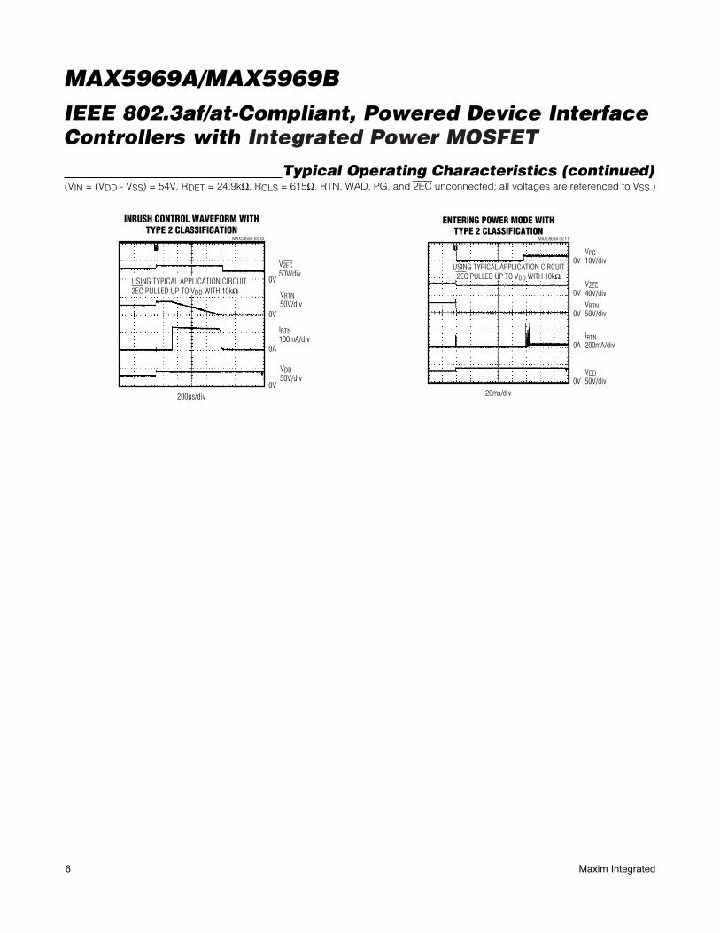
INRUSH CONTROL WAVEFORM WITHTYPE 2 CLASSIFICATION
MAX5969A toc10
0V
0V
0A
0V
VRTN50V/div
IRTN100mA/div
VDD50V/div
V2EC50V/div
200µs/div
USING TYPICAL APPLICATION CIRCUIT2EC PULLED UP TO VDD WITH 10kI
ENTERING POWER MODE WITHTYPE 2 CLASSIFICATION
MAX5969A toc11
VPG10V/div0V
0V
0V
0A
0V
VRTN50V/div
IRTN200mA/div
VDD50V/div
20ms/div
V2EC40V/div
USING TYPICAL APPLICATION CIRCUIT2EC PULLED UP TO VDD WITH 10kI

7Maxim Integrated
IEEE 802.3af/at-Compliant, Powered Device Interface Controllers with Integrated Power MOSFET
MAX5969A/MAX5969B
Pin Description
PIN NAME FUNCTION
1 VDD Positive Supply Input. Connect a 68nF (min) bypass capacitor between VDD and VSS.
2 DET Detection Resistor Input. Connect a signature resistor (RDET = 24.9kI) from DET to VDD.
3 N.C. No Connection. Not internally connected.
4 I.C. Internally Connected. Leave unconnected.
5 VSSNegative Supply Input. VSS connects to the source of the integrated isolation n-channel power MOSFET.
6 RTNDrain of Isolation MOSFET. RTN connects to the drain of the integrated isolation n-channel power MOSFET. Connect RTN to the downstream DC-DC converter ground as shown in the Typical Application Circuit.
7 WAD
Wall Power Adapter Detector Input. Wall adapter detection is enabled the moment VDD - VSS crosses the mark event threshold. Detection occurs when the voltage from WAD to RTN is greater than 9V. When a wall power adapter is present, the isolation n-channel power MOSFET turns off, 2EC current sink turns on. Connect WAD directly to RTN when the wall power adapter or other auxiliary power source is not used.
8 PGOpen-Drain Power-Good Indicator Output. PG sinks 230FA to disable the downstream DC-DC converter while turning on the hot-swap MOSFET switch until the hot-swap switch is fully on. PG current sink is disabled during detection, classification, and in the steady-state power mode.
9 2EC
Active-Low 2-Event Classification Detect or Wall Adapter Detect Output. A 1.5mA current sink is enabled at 2EC when a Type 2 PSE or a wall adapter is detected. When powered by a Type 2 PSE, the 2EC current sink is enabled and latched low after the isolation MOSFET is fully on until VIN drops below the UVLO threshold. 2EC also asserts when a wall adapter supply, typically greater than 9V, is applied between WAD and RTN. 2EC is not latched if asserted by WAD.
10 CLSClassification Resistor Input. Connect a resistor (RCLS) from CLS to VSS to set the desired classification current. See the classification current specifications in the Electrical Characteristics table to find the resis-tor value for a particular PD classification.
–– EPExposed Pad. Do not use EP as an electrical connection to VSS. EP is internally connected to VSS through a resistive path and must be connected to VSS externally. To optimize power dissipation, solder the exposed pad to a large copper power plane.

8 Maxim Integrated
IEEE 802.3af/at-Compliant, Powered Device Interface Controllers with Integrated Power MOSFET
MAX5969A/MAX5969B
Simplified Block Diagram
1.5mA
46µA
VDD
EN CLS1.23V
PSE 2
2EC
VDD
5V
11.6V/10.8V
11.6V/4V
D Q
Q
SET
CLR
DET
VSS
5V REGULATOR
5V
1.23V
22.8V/22V
THERMAL SHUTDOWN
QR
S
VDD
VDD
VDD
WAD
WAPD
RTN
VON/VOFF
VDD
D Q
Q
SET
CLR
9V
230µA
PG
CLASSIFICATION
ISWITCH
K x ISWITCH
ISOLATIONSWITCH
S
MUX
I0 135mA
VON/VOFF = 38.6V/31V FOR MAX5969BVON/VOFF = 35.4V/31V FOR MAX5969A
760mAI11/K
MAX5969AMAX5969B
95ms
HSON
4V
15V
IREF
9Maxim Integrated
IEEE 802.3af/at-Compliant, Powered Device Interface Controllers with Integrated Power MOSFET
MAX5969A/MAX5969B
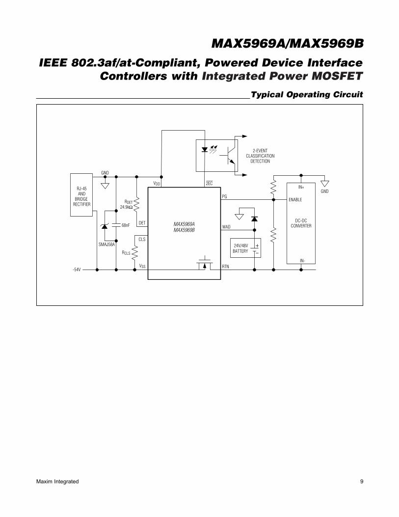
Typical Operating Circuit
2-EVENTCLASSIFICATION
DETECTION
-54V
MAX5969AMAX5969B
VDD
RTN
WAD
PG
2EC
24V/48VBATTERY
68nF
RJ-45AND
BRIDGE RECTIFIER
GND
SMAJ58A
RDET24.9kI
RCLS
VSS
DET
CLS
ENABLE
DC-DCCONVERTER
IN+
IN-
GND

10 Maxim Integrated
IEEE 802.3af/at-Compliant, Powered Device Interface Controllers with Integrated Power MOSFET
MAX5969A/MAX5969B
Detailed DescriptionOperating Modes
Depending on the input voltage (VIN = VDD - VSS), the MAX5969A/MAX5969B operate in four different modes: PD detection, PD classification, mark event, and PD power. The devices enter PD detection mode when the input voltage is between 1.4V and 10.1V. The device enters PD classification mode when the input voltage is between 12.6V and 20V. The device enters PD power mode once the input voltage exceeds VON.
Detection Mode (1.4V ≤ VIN ≤ 10.1V)In detection mode, the PSE applies two voltages on VIN in the range of 1.4V to 10.1V (1V step minimum) and then records the current measurements at the two points. The PSE then computes DV/DI to ensure the presence of the 24.9kω signature resistor. Connect the signature resistor (RDET) from VDD to DET for proper signature detection. The MAX5969A/MAX5969B pull DET low in detection mode. DET goes high impedance when the input voltage exceeds 12.5V. In detection mode, most of the MAX5969A/MAX5969B internal circuitry is off and the offset current is less than 10µA.
If the voltage applied to the PD is reversed, install protection diodes at the input terminal to prevent internal damage to the MAX5969A/MAX5969B (see the Typical Application Circuit). Since the PSE uses a slope technique (DV/DI) to calculate the signature resistance, the DC offset due to the protection diodes is subtracted and does not affect the detection process.
Classification Mode (12.6V ≤ VIN ≤ 20V)In the classification mode, the PSE classifies the PD based on the power consumption required by the PD. This allows the PSE to efficiently manage power distribution. Class 0 to 5 is defined as shown in Table 1. (The IEEE 802.3af/at standard defines only Class 0 to 4 and Class 5 for any special requirement.) An external resistor (RCLS) connected from CLS to VSS sets the classification current.
The PSE determines the class of a PD by applying a voltage at the PD input and measuring the current sourced out of the PSE. When the PSE applies a voltage between 12.6V and 20V, the MAX5969A/MAX5969B exhibit a current characteristic with a value shown in Table 1. The PSE uses the classification current information to classify the power requirement of the PD. The classification current includes the current drawn by RCLS and the supply current of the MAX5969A/MAX5969B so the total current drawn by the PD is within the IEEE 802.3af/at standard figures. The classification current is turned off whenever the device is in power mode.
2-Event Classification and DetectionDuring 2-event classification, a Type 2 PSE probes PD for classification twice. In the first classification event, the PSE presents an input voltage between 12.6V and 20V and the MAX5969A/MAX5969B present the pro-grammed load ICLASS. The PSE then drops the probing voltage below the mark event threshold of 10.1V and the MAX5969A/MAX5969B present the mark current (IMARK). This sequence is repeated one more time.
Table 1. Setting Classification Current
*VIN is measured across the MAX5969A/MAX5969B input VDD to VSS.
CLASS
MAXIMUM POWER USED
BY PD(W)
RCLS(I)
VIN*(V)
CLASS CURRENT SEEN AT VIN (mA)
IEEE 802.3af/at PSE CLASSIFICATION CURRENT
SPECIFICATION (mA)
MIN MAX MIN MAX
0 0.44 to 12.95 619 12.6 to 20 0 4 0 5
1 0.44 to 3.94 117 12.6 to 20 9 12 8 13
2 3.84 to 6.49 66.5 12.6 to 20 17 20 16 21
3 6.49 to 12.95 43.7 12.6 to 20 26 30 25 31
4 12.95 to 25.5 30.9 12.6 to 20 36 44 35 45
5 > 25.5 21.3 12.6 to 20 52 64 — —

11Maxim Integrated
IEEE 802.3af/at-Compliant, Powered Device Interface Controllers with Integrated Power MOSFET
MAX5969A/MAX5969B
When the MAX5969A/MAX5969B are powered by a Type 2 PSE, the 2-event identification output 2EC asserts low after the internal isolation n-channel MOSFET is fully turned on. 2EC current sink is turned off when VDD goes below the UVLO threshold (VOFF) and turns on when VDD goes above the UVLO threshold (VON), unless VDD goes below VTHR to reset the latched output of the Type 2 PSE detection flag.
Alternatively, the 2EC output also serves as a wall adapter detection output when the MAX5969A/MAX5969B are powered by an external wall power adapter. See the Wall Power Adapter Detection and Operation section for more information.
Power Mode (Wake Mode)The MAX5969A/MAX5969B enter power mode when VIN rises above the undervoltage lockout threshold (VON). When VIN rises above VON, the MAX5969A/MAX5969B turn on the internal n-channel isolation MOSFET to connect VSS to RTN with inrush current limit internally set to 135mA (typ). The isolation MOSFET is fully turned on when the voltage at RTN is near VSS and the inrush current is reduced below the inrush limit. Once the isolation MOSFET is fully turned on, the MAX5969A/MAX5969B change the current limit to 800mA. The open-drain power-good output (PG) remains low for a minimum of tDELAY until the power MOSFET fully turns on to keep the downstream DC-DC converter disabled during inrush.
Undervoltage LockoutThe MAX5969A/MAX5969B operate up to a 60V supply voltage with a turn-on UVLO threshold (VON) at 35.4V/38.6V and a turn-off UVLO threshold (VOFF) at 31V. When the input voltage is above VON, the MAX5969A/MAX5969B enter power mode and the internal MOSFET is turned on. When the input voltage goes below VOFF for more than tOFF_DLY, the MOSFET turns off.
Power-Good OutputThe enable pin of the downstream DC-DC control may see up to 375FA sinking current from PG to VSS. To be safe, make sure the downstream controller is capable of handling 375FA current out from the enable pin or adding a circuit to satisfy the absolute maxim rating of the enable pin.
Thermal-Shutdown ProtectionThe MAX5969A/MAX5969B include thermal protection from excessive heating. If the junction temperature exceeds the thermal-shutdown threshold of +140NC, the MAX5969A/MAX5969B turn off the internal power MOSFET and 2EC current sink. When the junction tem-perature falls below +112NC, the devices enter inrush mode and then return to power mode. Inrush mode ensures the downstream DC-DC converter is turned off as the internal power MOSFET is turned on.
Wall Power Adapter Detection and Operation
For applications where an auxiliary power source such as a wall power adapter is used to power the PD, the MAX5969A/MAX5969B feature wall power adapter detection. Once the input voltage (VDD - VSS) exceeds the mark event threshold, the MAX5969A/MAX5969B enable wall adapter detection. The wall power adapt-er is connected from WAD to RTN. The MAX5969A/MAX5969B detect the wall power adapter when the voltage from WAD to RTN is greater than 9V. When a wall power adapter is detected, the internal n-channel isolation MOSFET turns off, 2EC current sink turns on, and classification current is disabled if VIN is in the clas-sification range.

12 Maxim Integrated
IEEE 802.3af/at-Compliant, Powered Device Interface Controllers with Integrated Power MOSFET
MAX5969A/MAX5969B
Applications InformationOperation with 12V Adapter
Layout ProcedureCareful PCB layout is critical to achieve high efficiency and low EMI. Follow these layout guidelines for optimum performance:
1) Place the input capacitor, classification resistor, and transient voltage suppressor as close as possible to the MAX5969A/MAX5969B.
2) Use large SMT component pads for power dissipat-ing devices such as the MAX5969A/MAX5969B and the external diodes.
3) Use short and wide traces for high-power paths.
4) Use the MAX5969 Evaluation Kit layout as a refer-ence.
Figure 2. Typical Configuration When Using a 12V Wall Power Adapter
68nF
2-EVENT CLASSIFICATION(ASSERTED ON)
ENABLE
DC-DCCONVERTER
IN+
IN-
RJ-45AND
BRIDGE RECTIFIER
GND
GND
-54V
SMAJ58A
MAX5969AMAX5969B
RDET24.9kI
RCLS
VDD
VSS RTN
WAD
PG
DET
CLS
2EC
12VBATTERY
THIS CIRCUIT ACHIEVES PROPER 2EC LOGIC WHEN
BATTERY IS < 12.5V

13Maxim Integrated
IEEE 802.3af/at-Compliant, Powered Device Interface Controllers with Integrated Power MOSFET
MAX5969A/MAX5969B
Typical Application Circuit
68nF
ISOLATED 2-EVENTCLASSIFICATION
OUTPUT
GND
VAC
VAC
GND
-54V
SMAJ58A
MAX5969AMAX5969B
24.9kI
43.7I
VDD
VSS RTN
WAD
PGPG
DET
CLS
2EC
24/48VBATTERY
RTN
MAX15000
UVLO/EN IN
VCCUFLG
FB
COMP
CS
PG
CS
VCC
VCC
CS
RTN
ISOLATED +5.3V/2A
ISOLATED RTN
ISOLATED RTN
GNDRTN
GND 33kI
10kI
249I
22.1I
0.75I
1kI
619I 8.2nF
330pF
649I
4.99kI1kI 100pF
33nF
8.06kI
2.49kI
1kI18.1kI
RTN
4.99kI
NDRV
GND
RT
51.5kI1.37MI 0.1µF
0.1µF 0.1µF
0.1µF
22µF
4.7µF
2.2nF
8.06kI

14 Maxim Integrated
IEEE 802.3af/at-Compliant, Powered Device Interface Controllers with Integrated Power MOSFET
MAX5969A/MAX5969B
Package InformationFor the latest package outline information and land patterns, go to www.maximintegrated.com/packages. Note that a “+”, “#”, or “-” in the package code indicates RoHS status only. Package drawings may show a dif-ferent suffix character, but the drawing pertains to the package regardless of RoHS status.
Chip InformationPROCESS: BiCMOS
PACKAGE TYPE PACKAGE CODE DOCUMENT NO.
10 TDFN-EP T1033+1 21-0137

Maxim Integrated cannot assume responsibility for use of any circuitry other than circuitry entirely embodied in a Maxim Intagrated product. No circuit patent licenses are implied. Maxim Integrated reserves the right to change the circuitry and specifications without notice at any time. The parametric values (min and max limits) shown in the Electrical Characteristics table are guaranteed. Other parametric values quoted in this data sheet are provided for guidance.
Maxim Integrated 160 Rio Robles, San Jose, CA 95134 USA 1-408-601-1000 15© 2015 Maxim Integrated Products, Inc. Maxim Integrated and the Maxim Integrated logo are trademarks of Maxim Integrated Products, Inc.
IEEE 802.3af/at-Compliant, Powered Device Interface Controllers with Integrated Power MOSFET
MAX5969A/MAX5969B
Revision HistoryREVISIONNUMBER
REVISIONDATE
DESCRIPTIONPAGES
CHANGED
0 12/09 Initial release —
1 7/15 Revised Power-Good Output section 11
Recommended