midi LOGGER dual
SERVICE MANUAL
500MANUAL NO. GL500-UM-251
GL500-UM-251-03-9370


GL500-UM-251-9370 i
HISTORY OF REVISIONSNo. Date issued Description of revision Page Edition1 05.02.15 First Printing All 012 05.03.22 Note was added for upgrading the firmware. 2-1 023 05.12.01 Part numbers were added for the AC power cables 6-1 03

GL500-UM-251-9370 ii
TO ENSURE SAFETYThis Service Manual has been compiled for the purpose of facilitating repair and maintenance of the GL500
midi LOGGER dual by Graphtec service personnel and other persons who have undergone equivalent
technical training.
Maintenance or repair by unauthorized service personnel is to be strictly avoided. Because the GL500
contains numerous internal components with a high electric potential, such work by unauthorized service
personnel could cause human injury or serious damage to the GL500 midi LOGGER dual.

GL500-UM-251-9370 iii
CONTENTS1. CONFIGURATION .................................................................................. 1-1
1.1 Model Configuration ................................................................................................... 1-1
1.2 Accessories and Options ........................................................................................... 1-1
2. UPGRADING THE FIRMWARE ............................................................. 2-12.1 How to Upgrade the GL500 Flash ROM from the PCMCIA Card ............................. 2-1
2.2 How to Upgrade the GL500 Flash ROM from the TCP/IP or USB Port ................... 2-2
3. DISASSEMBLY AND REASSEMBLY .................................................... 3-13.1 Notes on Disassembly and Reassembly .................................................................. 3-1
3.2 Mounting and Removing the Input Terminal Unit .................................................... 3-1
3.3 Replacing the Main Control Board ............................................................................3-3
3.4 Replacing the Memory Control Board .......................................................................3-5
3.5 Replacing the LCD .......................................................................................................3-6
4. SETUP PROCEDURES .......................................................................... 4-14.1 Entering the System Setup Menu .............................................................................. 4-1
4.2 Setup1 (Voltage Input) ................................................................................................4-2
4.3 Setup2 (Room Temperature Compensation) ............................................................4-5
5. INSPECTION AND CHECK PROCEDURES ......................................... 5-15.1 Insulation Resistance ................................................................................................. 5-1
5.2 How to Load the Condition Settings Files ................................................................5-2
5.3 Voltage Accuracy ........................................................................................................5-4
5.4 Temperature Accuracy ................................................................................................5-8
5.5 Frequency and Filter Characteristics ...................................................................... 5-14
5.6 Memory and Trigger Functions ................................................................................ 5-19
5.7 Signal-to-Noise Ratio ................................................................................................5-23
5.8 Key Test ......................................................................................................................5-27
6. PARTS LISTS ......................................................................................... 6-16.1 Recommended Parts List ........................................................................................... 6-1
6.2 Standard Accessories ................................................................................................. 6-1
6.3 Parts Lists ....................................................................................................................6-2
6.3.1 Top Cover .............................................................................................................................. 6-26.3.2 LCD & Key Panel .................................................................................................................. 6-36.3.3 Top Cover, Reverse Side ...................................................................................................... 6-46.3.4 Main Frame ........................................................................................................................... 6-56.3.5 Bottom Case ......................................................................................................................... 6-66.3.6 Input Terminal Unit .................................................................................................................6-7
7. BLOCK DIAGRAMS .............................................................................. 7-1

GL500-UM-251-9370 iv

GL500-UM-251-9370 1-1
1. CONFIGURATION
1. CONFIGURATION
1.1 Model ConfigurationGL500VF : 4-channel VF amp model (4-channel isolated voltage amp)
GL500MF : 4-channel MF amp model (4-channel isolated voltage / temperature amp)
GL500MS : 8-channel MS amp model (8-channel non-isolated voltage / temperature amp)
1.2 Accessories and Options
Unit name Model name DescriptionBattery Pack B-517Pulse / Logic / Alarm Cable B-513 Same as GL400/350DC Drive Cable B-514 Same as GL400/350T-type Thermocouple JBS-7115-5M-TK-type Thermocouple JBS-7115-5M-KBNC-BNC Cable RIC-112 1.5 mBNC-Banana Cable RIC-113 1.5 mBNC-Alligator Cable RIC-114 1.5 m

GL500-UM-251-9370 1-2
1. CONFIGURATION

GL500-UM-251-9370 2-1
2. UPGRADING THE FIRMWARE
2. UPGRADING THE FIRMWAREThe version of your GL500’s firmware can be upgraded by rewriting the flash ROM on the pertinent circuit
boards using a choice of methods. You can upgrade the firmware by loading the upgrade program from either
a PCMCIA card or from a personal computer via the TCP/IP or USB port.
2.1 How to Upgrade the GL500 Flash ROM from the PCMCIA Card
Preparations for the upgrade
Firmware :Mxxxa001.G50 ← Main Program file for GL500
:Mxxxa002.G50 ← Main Program file for GL500
(1) Connect the AC adapter for the GL500.
(2) Turn on the GL500 and then adjust the monitor contrast using the monitor control dial when you are
going to upgrade the GL500.
Turn off the GL500 after adjust the monitor contrast.
(3) Copy the two main program files to a PCMCIA card from the computer.
How to upgrade
(1) Insert the PCMCIA card containing the main upgrade program into the GL500's PCMCIA card slot.
(2) Turn on the GL500 to automatically execute the upgrade program.
(3) Wait until the display shown below appears or until the beeper sound stops.
Note:
Don't turn off the GL500 until this process is finished.
The following message will appear on the GL500 display in yellow characters when the upgrade is
complete. Also, the beeper will sound for 5 seconds.
“Please Turn Off the Power. I have locked up.”
Note:
Adjust the the monitor contrast using the monitor control dial when the above message will not appear
on the GL500.
(4) Turn off the power to the GL500 when the above message is displayed or when the beeper sound
stops.
(5) Delete the two main program files in a PCMCIA card from the computer.
This is avoiding to upgrade by mistake.

GL500-UM-251-9370 2-2
2. UPGRADING THE FIRMWARE
2.2 How to Upgrade the GL500 Flash ROM from the TCP/IP or USB Port
Preparations for the upgrade
(1) Connect the AC adapter for the GL500.
(2) Connect the LAN cable or USB cable for the GL500 and PC.
When using the TCP/IP port for the upgrade, use a cross LAN cable if you connect P to P. If you
connect via a hub, use a parallel LAN cable.
(3) If you are going to use the TCP/IP port for the upgrade, confirm the IP address of the GL500 as shown
below.
The default settings for the GL500 are set as follows.
IP Address: 192.168.0.1
Subnet mask: 255.255.255.0
Port number: 8023
If you haven’t changed them, use these settings.
Also, your computer’s TCP/IP port setting must be set to the same segment as “192.168.0.X”.
How to upgradeOS :Windows 2000/XP
Software :GL50upd.exe ← Upgrade software file
:xxx.dll ← Upgrade software dll file
Firmware :Mxxxa001.G50 ← Main Program file for GL500
:Mxxxa002.G50 ← Main Program file for GL500
(1) Copy the two upgrade software files to the same directory in the PC.
(2) Turn on the power switch of the GL500.
(3) Execute GL50upd.exe.
GL500-UM-251-9370 2-3
2. UPGRADING THE FIRMWARE
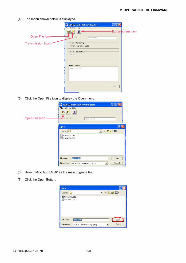
(4) The menu shown below is displayed.
Open File Icon
Transmission Icon
Exit program Icon
(5) Click the Open File icon to display the Open menu.
Open File Icon
(6) Select ”MxxxA001.G50" as the main upgrade file.
(7) Click the Open Button.

GL500-UM-251-9370 2-4
2. UPGRADING THE FIRMWARE
(8) If you need to change the TCP/IP settings or port, click the transmission icon to set up the TCP/IP
conditions or port.
Transmission Icon
The default settings for the GL500 are set as follows.
IP Address: 192.168.0.1
Port number: 8023
If you haven’t changed them, use these settings.
Also, your computer’s TCP/IP port setting must be set to the same segment as “192.168.0.X”.
If you are using the USB port, select USB for Transfer I/F in the above menu.
(9) Click the Start button to start upgrading when you are ready to upgrade.
The following message will appear on the GL500 display in yellow characters when the upgrade is
complete. Also, the beeper will sound for 5 seconds.
“Please Turn Off the Power. I have locked up.”
(10) Turn off the power to the GL500 when the above message is displayed or when the beeper sound
stops.

GL500-UM-251-9370 2-5
2. UPGRADING THE FIRMWARE

GL500-UM-251-9370 3-1
3. DISASSEMBLY AND REASSEMBLY
3. DISASSEMBLY AND REASSEMBLY
3.1 Notes on Disassembly and Reassembly• During disassembly, disconnect the cables from the specified connectors as necessary.
• During reassembly, double-check to ensure that the proper cables have been correctly re-connected to
the pertinent connectors.
• Some areas of the control panel unit possess a high electrical potential, so exercise caution to avoid an
electrical shock.
• When handling the LCD shield and LCD protective plate, be careful not to leave fingerprints or other
marks on them.
3.2 Mounting and Removing the Input Terminal UnitThis section describes how to mount and remove the input terminal unit.
CAUTION
• Make sure that the power supply has been turned off before mounting or removing the input terminal unit.
Removing the Input Terminal Unit
(1) Remove the cover from the input terminal mounting area.
(2) Press down on the lock button while pulling the input terminal unit towards you. At this time, grip the
input terminal unit firmly while removing it.

GL500-UM-251-9370 3-2
3. DISASSEMBLY AND REASSEMBLY
Mounting the Input Terminal Unit
(1) Remove the cover from the input terminal mounting area.
(2) As shown in the figure below, insert the input terminal unit in the GL500. At this time, be sure to check
that the terminal unit is locked onto the connector.

GL500-UM-251-9370 3-3
3. DISASSEMBLY AND REASSEMBLY
3.3 Replacing the Main Control Board
Disassembly
(1) Remove the input terminal unit from the GL500 (See Section 3.2.).
(2) Remove the M3L30 binding head screw and the four M3L10 self tapping screws from the bottom cover.
(3) Release the top cover hook from the bottom case, and then remove the top cover assembly.
NOTE:
Take care with the flexible cable connecting the top cover assembly and the bottom case assembly when you are
removing the top cover assembly for the GL500.
(4) Disconnect the flexible cable from the main control board for the GL500.
Hook
Top cover assembly
Bottom case assembly
M3L30 bindinghead screw
M3L10 self tapping screw

GL500-UM-251-9370 3-4
3. DISASSEMBLY AND REASSEMBLY
(5) Remove the four M2.6L6 binding head screws holding the main control board and AMP shield sheet,
and then remove the main control board from the bottom case assembly.
Insert this side first when installing the main control board to the bottom case assembly.
Spacer
M2.6L6 bindinghead screw
Main control board
AMP shield sheet
Re-assembly
(1) Re-assemble the main control board in the reverse order in which it was disassembled.
(2) Set up the GL500 when you replace any of the boards.

GL500-UM-251-9370 3-5
3. DISASSEMBLY AND REASSEMBLY
3.4 Replacing the Memory Control Board
Disassembly
(1) Remove the input terminal unit from the GL500 (See Section 3.2.).
(2) Remove the main control board from the bottom case (See Section 3.3.).
(3) Remove the four M2.6L6 binding head screws holding the memory control board, and then detach the
memory control board from the bottom case assembly.
Memory control
board
M2.6L6 binding
head screw
AMP sheet
Re-assembly
(1) Re-assemble the memory control board in the reverse order in which it was disassembled.
(2) Re-assemble the other parts in the reverse order in which they were disassembled.
(3) Set up the GL500 when you replace any of the boards.

GL500-UM-251-9370 3-6
3. DISASSEMBLY AND REASSEMBLY
3.5 Replacing the LCD
Disassembly
(1) Remove the input terminal unit from the GL500 (See Section 3.2.).
(2) Disconnect the LCD flexible cable from the control panel board.
Top cover assembly
Control panel board
LCDLCD flexible cable
(3) Remove the one M2.6 binding head screw holding the LCD unit, and then detach the LCD unit.
M2.6 binding head screw
LCD unit

GL500-UM-251-9370 3-7
3. DISASSEMBLY AND REASSEMBLY
Re-assembly
(1) Re-assemble the LCD unit in the reverse order in which it was disassembled.

GL500-UM-251-9370 4-1
4. SETUP PROCEDURES
4. SETUP PROCEDURES
4.1 Entering the System Setup Menu
(1) Press the [MENU] key, and then press the [Right Direction] key until the “INFO” menu shown below
appears.
(2) Press the [UP Direction] key 10 times in order to display the “Setup Menu” shown below.
(3) Move the cursor to the “Mode” position using the [Direction] keys.
(4) Press the [ENTER] key to display the menu below from which you can execute the Setup operations.
Setup modeSetup1 (Basic)Setup2 (Room temp.)
(5) Select the Setup mode using the [Direction] keys, and then press the [ENTER] key.
(6) Move the cursor to the “Execute Setup” position as shown above.
(7) Press the [ENTER] key to start the selected Setup operation.

GL500-UM-251-9370 4-2
4. SETUP PROCEDURES
4.2 Setup1 (Voltage Input)This procedure is required when any part of the AMP board is replaced or the main board is replaced.
This procedure is required for all the amps (VF, MF and MS amps).
Preparation
• Have a voltage generator on hand that can output voltage up to 100 VDC (four-digit output).
• Mutually connect the ground terminals of the voltage generator and the GL500.
Wiring connection
Voltage generator
AC adapter
Connect to all channels
Input cable
Connect both ends to GND
Multimeter

GL500-UM-251-9370 4-3
4. SETUP PROCEDURES
Setup procedure
(1) As shown in the figure above, connect the output of the voltage generator to the GL500’s input terminal.
(2) Leave the GL500 turned on for at least 30 minutes.
(3) After entering the System Setup mode, open the Setup Menu as shown below.
Specify the AMP Setup conditions as shown below.
Setup CH :ALL
AMP type :VF, MF, or MS (select the amp type for setup)
Mode :Setup1 (Basic)
(4) Move the cursor to the “Execute Setup” position as shown above.
(5) Press the [ENTER] key to start the Setup1 (Basic) operation.
Message

GL500-UM-251-9370 4-4
4. SETUP PROCEDURES
(6) The “GND : [START]” message is displayed at the location shown above.
(7) Input “0.000mV” to the input terminals of channel 1.
(8) Press the [START] key and then wait until the "20 mV : [START]" message appears.
Specify the voltage generator's output voltage setting to correspond to one of the displayed voltage
ranges in the following table, and then input that voltage to the GL500.
Message Input Voltage RemarksGND 0.000 mV
20 mV 20.000 mV50 mV 50.000 mV100 mV 100.000 mV500 mV 500.000 mV
1 V 1.000 V5 V 5.000 V10 V 10.000 V50 V 50.000 V Not required for the MS amp100 V 100.00 V Not required for the MS amp
(9) Repeat step (8) by sequentially setting the Measure parameter to 50 mV, 100 mV, 500 mV, 1 V, 5 V, 10 V,
(50 V) and (100 V ), and then inputting the corresponding voltage.
50 V and 100 V are not required for setup of the MS amp.
(10) When you have finished the Setup operation for 100 V (10V), the "EEPROM : [ENTER]" message
appears.
Press the [ENTER] key to begin writing the new Setup data to the EEPROM.
(11) After the setup parameters have been registered to the EEPROM, the display closes and returns to
normal mode.
(12) Turn off the GL500.
This completes the voltage amp setup.

GL500-UM-251-9370 4-5
4. SETUP PROCEDURES
4.3 Setup2 (Room Temperature Compensation)This procedure is required for the MF and MS amps.
Preparation
As shown below, use (T) temperature compensation leads to connect the target amps to the 0˚C reference
temperature device (Zero controller). Also be sure to use (T) temperature compensation leads to connect the
input terminal.
Wiring connection
AC adapter
(T) compensation lead
(T) input side
(T) output side
0˚C referencetemperature device(Zero Controller)
Input 0 V for the output side or short the + and - terminals
Connect both ends to GND
CAUTION
Connect each compensation copper lead to a single terminal as shown in the above diagram (parallel
wiring is not permitted).
(1) As shown in the figure above, connect the input of the zero controller to the GL500’s input terminal.
(2) Leave the GL500 turned on for at least 30 minutes.

GL500-UM-251-9370 4-6
4. SETUP PROCEDURES
(3) After entering the System Setup mode, open the Setup Menu as shown below.
Specify the AMP Setup conditions as shown below.
Setup CH :ALL
AMP type :MF, or MS (select the amp type for setup)
Mode :Setup2 (Room temp.)
(4) Move the cursor to the “Execute Setup” position as shown above.
(5) Press the [ENTER] key to start the Setup2 (Room temp.) operation.
Message
(6) The “rTemp : [START]” message is displayed at the location shown above.
(7) Press the [START] key and then wait until the "EEPROM : [ENTER]" message appears.
(8) Press the [ENTER] key to begin writing the new Setup data to the EEPROM.
(9) After the setup parameters have been registered to the EEPROM, the display closes and returns to
normal mode.
(10) Turn off the GL500.
This completes the Room temp. setup.

GL500-UM-251-9370 5-1
5. INSPECTION AND CHECK PROCEDURES
5. INSPECTION AND CHECK PROCEDURES
5.1 Insulation ResistanceUse a megohm meter (an insulation resistance gauge) to check that the insulation resistance between the
following terminals is equal to or higher than the rated value.
This inspection is not required for the 8MS amp.
Measuring Terminals Rated value RemarksCh1- to GND (FG)
Ch2- to GND (FG)
Ch3- to GND (FG)
Ch4- to GND (FG)
Megohm meter with an
output capacity of 500
VDC; insulation resistance
is 50 M ohm or more.
Check the ( - ) terminal of
each channel, one by one.
Wiring connection500 V megohm meter
AC adapter
MF amp VF amp
Connect both ends to GND
Connect to the minus terminal of channels 1 to 4, one by one.

GL500-UM-251-9370 5-2
5. INSPECTION AND CHECK PROCEDURES
5.2 How to Load the Condition Settings Files
Preparations for inspections and checks
Condition settings files :CondVFV.CND ← Condition settings for the voltage accuracy of the VF amp
:CondMFV.CND ← Condition settings for the voltage accuracy of the MF amp
:CondMSV.CND ← Condition settings for the voltage accuracy of the MS amp
:CondMFT.CND ← Condition settings for the T range accuracy of the MF amp
:CondMFK.CND ← Condition settings for the K range accuracy of the MF amp
:CondMST.CND ← Condition settings for the T range accuracy of the MS amp
:CondMSK.CND ← Condition settings for the K range accuracy of the MS amp
:CondVFoff.CND ← Condition settings for the frequency and filter
characteristics of the VF amp when Off was specified for
Filter
:CondMFoff.CND ← Condition settings for the frequency and filter
characteristics of the MF amp when Off was specified for
Filter
CondMSoff.CND ← Condition settings for the frequency and filter
characteristics of the MS amp when Off was specified for
Filter
:CondVFM.CND ← Condition settings for the memory and trigger functions of
the VF amp
:CondMFM.CND ← Condition settings for the memory and trigger functions of
the MF amp
:CondMSM.CND ← Condition settings for the memory and trigger functions of
the MS amp
:CondVFsn.CND ← Condition settings for the signal-to-noise ratio of the VF
amp
:CondMFsn.CND ← Condition settings for the signal-to-noise ratio of the MF
amp
:CondMSsn.CND ← Condition settings for the signal-to-noise ratio of the MS
amp
(1) Copy the above condition settings files to a PCMCIA card from the computer.

GL500-UM-251-9370 5-3
5. INSPECTION AND CHECK PROCEDURES
How to load the condition settings files to the GL500 from a PCMCIA card
(1) Press the [MENU] key, and then press the [Right Direction] key until the “FILE” menu shown below
appears.
(2) Move the cursor to the “Load settings” position using the [Direction] keys.
(3) Press the [ENTER] key to display the menu shown below.
(4) Specify the condition settings file to execute the various inspection operations.
(5) Move the cursor to the “Execute” position using the [Direction] keys.
(6) Press the [ENTER] key to load the condition settings file.
(7) Press the [QUIT] key to exit the menu mode.

GL500-UM-251-9370 5-4
5. INSPECTION AND CHECK PROCEDURES
5.3 Voltage AccuracySupply the reference voltage or frequency determined for each measurement range, and then check the
voltage accuracy.
Preparation
• Use a voltage generator that can output up to 100 VDC (using four-digit settings).
• Mutually connect the ground terminals of the voltage generator and the GL500 prior to initiating
measurement.
• Install the amp for which you want to perform the voltage accuracy measurement procedure in the GL500.
Wiring connection
Same wiring connection as Setup1. (See the Setup1 procedure)
Setting procedure
(1) Load the condition settings file from the PCMCIA card for each amp type according to the table below.
Amp Condition file name RemarksVF amp CondVFV.CNDMF amp CondMFV.CNDMS amp CondMSV.CND
Measurement procedure
The procedure for the VF amp is explained here.
Perform this procedure for the other amps in the same way.
(1) Press the [MENU] key to display the menu shown below.
(2) Move the cursor to the CH: ALL : Range position as shown above.

GL500-UM-251-9370 5-5
5. INSPECTION AND CHECK PROCEDURES
(3) Press the [ENTER] key to display the menu shown below, and then select the reference voltage range.
(4) Press the [QUIT] key to display the menu shown below.

GL500-UM-251-9370 5-6
5. INSPECTION AND CHECK PROCEDURES
(5) Input the reference voltage for each range according to the table below, and then check that the level of
measurement is within the rating.
Voltage precision ratingsNo. Range Input voltage Rating (±025%) Remarks1 100 mV 0.00 mV -0.25 mV to +0.25 mV2 100 mV 100.00 mV +99.75 mV to +100.25 mV3 100 mV -100.00 mV -100.25 mV to -99.75 mV4 500 mV 500.0 mV 498.75 mV to +501.25 mV5 1 V 1.0000 V 0.9975 V to 1.0025 V6 5 V 5.000 V 4.9875 V to 5.0125 V7 10 V 10.000 V 9.975 V to 10.025 V8 50 V 50.00 V 49.875 V to 50.125 V Not required for the MS amp9 100 V 100.00 V 99.75 V to 100.25 V Not required for the MS amp
(6) Press the [START/STOP] key when the input voltage stabilizes.
(7) Wait until the "Free Running" message is displayed as shown below.
Message
(8) Press the [REVIEW] key to display the menu shown below.
Data Replay
Data Type:
Screen type:Execute:
Current Memory1-screen view
[ENTER]select/[QUIT]Exit
Move the cursor to the Execute position.
(9) Move the cursor to the Execute position as shown above.

GL500-UM-251-9370 5-7
5. INSPECTION AND CHECK PROCEDURES
(10) Press the [ENTER] key to display the menu shown below.
(11) Press the [MENU] key to display the menu shown below.
Move the cursor to the Execute position.
(12) Move the cursor to the Execute position as shown above.
(13) Press the [ENTER] key to display the menu shown below.
Confirm that these values are within the above ratings
after data has been captured.
(14) Press the [QUIT] key twice to exit the Current Review menu.
(15) Repeat steps (1) to (14), and confirm that each value is within the above ratings.

GL500-UM-251-9370 5-8
5. INSPECTION AND CHECK PROCEDURES
5.4 Temperature AccuracyThis procedure is required for the MF and MS amps.
Preparation
As shown below, use (T) temperature compensation leads to connect the target amps to the 0˚C reference
temperature device (Zero controller). Also be sure to use (T) temperature compensation leads to connect the
input terminal.
Install the amp for which you want to perform the temperature accuracy measurement procedure in the
GL500.
Wiring connection
AC adapter
(T) compensation lead
(T) input side
(T) output side
0˚C referencetemperature device(Zero Controller)
Input 0 V for the output side or short the + and - terminals
Connect both ends to GND
CAUTION
Connect each compensation copper lead to a single terminal as shown in the above diagram (parallel
wiring is not permitted).

GL500-UM-251-9370 5-9
5. INSPECTION AND CHECK PROCEDURES
Setting procedure
(1) Load the condition settings files from the PCMCIA card.
Condition settings files :CondMFT.CND ← Condition settings for the T range accuracy of the MF amp
:CondMFK.CND ← Condition settings for the K range accuracy of the MF amp
:CondMST.CND ← Condition settings for the T range accuracy of the MS amp
:CondMSK.CND ← Condition settings for the K range accuracy of the MS amp
Measurement procedure (temperature accuracy)
The procedure for the MF amp is explained here.
Perform this procedure for the MS amp in the same way.
(1) Load the condition settings file for type T as described above.
(2) Connect to the zero controller with the (T) compensation leads.
(3) Press the [ENTER] key to display the menu shown below, and then confirm the settings.
(4) Press the [QUIT] key to display the menu shown below.
GL500-UM-251-9370 5-10
5. INSPECTION AND CHECK PROCEDURES
(5) Input the reference voltage signal for each range to the 0˚C reference temperature device (zero
controller) according to the table below, then check that the level of measurement is within the rating.
Input voltage precision ratings (Type T)Temperature Input voltage Standard
0 ˚C 0.000 mV -2.0 ˚C to +2.0 ˚C
(6) Press the [START/STOP] key when the input voltage stabilizes.
(7) Wait until the "Free Running" message is displayed as shown below.
Message
(8) Press the [REVIEW] key to display the menu shown below.
Data Replay
Data Type:
Screen type:Execute:
Current Memory1-screen view
[ENTER]select/[QUIT]Exit
Move the cursor to the Execute position.
(9) Move the cursor to the Execute position as shown above.

GL500-UM-251-9370 5-11
5. INSPECTION AND CHECK PROCEDURES
(10) Press the [ENTER] key to display the menu shown below.
(11) Press the [MENU] key to display the menu shown below.
Move the cursor to the Execute position.
(12) Move the cursor to the Execute position as shown above.
(13) Press the [ENTER] key to display the menu shown below.
Confirm that these values are within the above ratings
after data has been captured.
(14) Confirm that each value is within the above ratings.
(15) Press the [QUIT] key twice to exit the Current Review menu.

GL500-UM-251-9370 5-12
5. INSPECTION AND CHECK PROCEDURES
(16) Connect (K) compensation leads to each amp.
(17) Load the condition settings file for type K as described above.
(18) Input the reference voltage signal for each range to the 0˚C reference temperature device (zero
controller) according to the table below, then check that the level of measurement is within the rating.
Input voltage precision ratings (Type K)Temperature Input voltage Standard
0 ˚C 0.000 mV -2.5 ˚C to +2.5 ˚C
(19) Press the [START/STOP] key when the input voltage stabilizes.
(20) Wait until the "Free Running" message is displayed as shown below.
Message
(21) Press the [REVIEW] key to display the menu shown below.
Data Replay
Data Type:
Screen type:Execute:
Current Memory1-screen view
[ENTER]select/[QUIT]Exit
Move the cursor to the Execute position.
(22) Move the cursor to the Execute position as shown above.

GL500-UM-251-9370 5-13
5. INSPECTION AND CHECK PROCEDURES
(23) Press the [ENTER] key to display the menu shown below.
(24) Press the [MENU] key to display the menu shown below.
Move the cursor to the Execute position.
(25) Move the cursor to the Execute position as shown above.
(26) Press the [ENTER] key to display the menu shown below.
Confirm that these values are within the above ratings
after data has been captured.
(27) Confirm that each value is within the above ratings.
(28) Press the [QUIT] key twice to exit the Current Review menu.

GL500-UM-251-9370 5-14
5. INSPECTION AND CHECK PROCEDURES
5.5 Frequency and Filter Characteristics
Preparation
• Have on hand an oscillator capable of the types of output described below.
Output waveforms : sine waves
Frequency : 5.0 Hz to 20.05 KHz
• Mutually connect the GND terminals of the oscillator and GND terminal of the GL500 before measurement.
Wiring connection
Connect the oscillator to all the amp input terminals.
Oscillator
10.000 KHzAC adapter
Connect the oscillator to all the amp input terminals.
Setting procedure
(1) Load the condition settings file from the PCMCIA card for each amp type according to the list below.
Condition settings files :CondVFoff.CND ← Condition settings for the frequency and filter
characteristics of the VF amp when Off was selected for
Filter
:CondMFoff.CND ← Condition settings for the frequency and filter
characteristics of the MF amp when Off was selected for
Filter
:CondMSoff.CND ← Condition settings for the frequency and filter
characteristics of the MS amp when Off was selected for
Filter

GL500-UM-251-9370 5-15
5. INSPECTION AND CHECK PROCEDURES
Measurement procedure
The procedure for the VF amp is explained here.
Perform this procedure for the other amps in the same way.
(1) Load the condition settings file CondVFoff.CND as described above.
(2) Press the [MENU] key to display the menu shown below.
(3) Press the [QUIT] key to display the menu shown below.
(4) Input the reference signal for each amp according to the table below, and then check that the measured
amplitude is within the rating when compared with the amplitude during reference signal input.Amp settings Generator output settings Rating
Input Range Filter Frequency AMPTD FCTN Rating (1 V input)
DC 1 V
OFF 20.05 KHz
1 V p-p Sine wave
0.65 V to 1.12V Line 1.5 Hz 0.55 V to 0.85V 5 Hz 5 Hz 0.55 V to 0.85V 50 Hz 50 Hz 0.6 V to 0.8 V 500 Hz 500 Hz 0.6 V to 0.8 V
(5) Press the [START/STOP] key.

GL500-UM-251-9370 5-16
5. INSPECTION AND CHECK PROCEDURES
(6) Wait until the "Free Running" message is displayed as shown below.
Message
(7) Press the [REVIEW] key to display the menu shown below.
Data Replay
Data Type:
Screen type:Execute:
Current Memory1-screen view
[ENTER]select/[QUIT]Exit
Move the cursor to the Execute position.
(8) Move the cursor to the Execute position as shown above.
(9) Press the [ENTER] key to display the menu shown below.

GL500-UM-251-9370 5-17
5. INSPECTION AND CHECK PROCEDURES
(10) Press the [MENU] key to display the menu shown below.
Move the cursor to the Execute position.
(11) Move the cursor to the Execute position as shown above.
(12) Press the [ENTER] key to display the menu shown below.
Confirm that these values are within the above ratings
after data has been captured.
(13) Press the [QUIT] key twice to exit the Current Review menu.
(14) Press the [MENU] key to display the menu shown below.

GL500-UM-251-9370 5-18
5. INSPECTION AND CHECK PROCEDURES
(15) Set the filter setting to the next filter setting as shown above.
(16) Repeat steps (3) to (13), and confirm that each value is within the above rating.

GL500-UM-251-9370 5-19
5. INSPECTION AND CHECK PROCEDURES
5.6 Memory and Trigger Functions
Preparation
• Have on hand an oscillator capable of the types of output described below.
Output waveforms : sine waves
Frequency : 1 Hz
• Mutually connect the GND terminals of the oscillator and GND terminal of the GL500 before measurement.
Wiring connection
Connect the oscillator to the channel 1 input terminal of the amp.
Oscillator
10.000 KHzAC adapter
Connect the oscillator to the channel 1 input terminal of the amp.
Setting procedure
(1) Load the condition settings file from the PCMCIA card for each amp type according to the list below.
Condition settings files :CondVFM.CND ← Condition settings for the memory and trigger functions of
the VF amp
:CondMFM.CND ← Condition settings for the memory and trigger functions of
the MF amp
:CondMSM.CND ← Condition settings for the memory and trigger functions of
the MS amp

GL500-UM-251-9370 5-20
5. INSPECTION AND CHECK PROCEDURES
Measurement procedure
The procedure for the VF amp is explained here.
Perform this procedure for the other amps in the same way.
(1) Load the condition settings file CondVFM.CND as described above.
(2) Press the [MENU] key to display the menu shown below.
(3) Press the [QUIT] key to display the menu shown below.
(4) Input the reference signal for each amp according to the table below, and then check that the measured
amplitude is within the rating when compared with the amplitude during reference signal input.Amp settings Generator output settings
Input Range Filter Frequency AMPTD FCTNDC 1 V OFF 1.00 Hz 1 V p-p Sine wave
(5) Press the [START/STOP] key to start data capture.

GL500-UM-251-9370 5-21
5. INSPECTION AND CHECK PROCEDURES
(6) Wait until the "Free Running" message is displayed as shown below.
Message
(7) Press the [REVIEW] key to display the menu shown below.
Data Type : Event
Block No. : 1
Data Replay
Data Type:
Block No.:Execute:
Event1
[ENTER]select/[QUIT]Exit
Move the cursor to the Execute position.
1
(8) Move the cursor to the Execute position as shown above.

GL500-UM-251-9370 5-22
5. INSPECTION AND CHECK PROCEDURES
(9) Press the [ENTER] key to display the menu shown below.
Trigger point
(10) Confirm that the captured waveform is similar to the one shown above.
(11) Press the [QUIT] key twice to exit the Current Review mode.
(12) Repeat steps (1) to (11) for each amp, and confirm that each captured waveform is similar to the one
shown above.

GL500-UM-251-9370 5-23
5. INSPECTION AND CHECK PROCEDURES
5.7 Signal-to-Noise Ratio
Wiring connection
Short the + and - terminals for all channels.
AC adapter
MF or MS amp VF amp
Short the + and - terminals for all channels.
Setting procedure
(1) Load the condition settings file from the PCMCIA card for each amp type according to the list below.
Condition settings files :CondVFsn.CND ← Condition settings for the signal-to-noise ratio of the VF
amp
:CondMFsn.CND ← Condition settings for the signal-to-noise ratio of the MF
amp
:CondMSsn.CND ← Condition settings for the signal-to-noise ratio of the MS
amp

GL500-UM-251-9370 5-24
5. INSPECTION AND CHECK PROCEDURES
Measurement procedure
The procedure for the VF amp is explained here.
Perform this procedure for the other amps in the same way.
(1) Load the condition settings file CondVFsn.CND as described above.
(2) Press the [MENU] key to display the menu shown below.
(3) Press the [QUIT] key to display the menu shown below.
(4) Press the [START/STOP] key to start data capture.

GL500-UM-251-9370 5-25
5. INSPECTION AND CHECK PROCEDURES
(5) Wait until the "Free Running" message is displayed as shown below.
Message
(7) Press the [REVIEW] key to display the menu shown below.
Data Replay
Data Type:
Screen type:Execute:
Current Memory1-screen view
[ENTER]select/[QUIT]Exit
Move the cursor to the Execute position.
(8) Move the cursor to the Execute position as shown above.

GL500-UM-251-9370 5-26
5. INSPECTION AND CHECK PROCEDURES
(9) Press the [ENTER] key to display the menu shown below.
(10) Press the [MENU] key to display the menu shown below.
Move the cursor to the Execute position.
(11) Move the cursor to the Execute position as shown above.
(12) Press the [ENTER] key to display the menu shown below.
Confirm that these values are within the ratings after
data has been captured.
(13) Confirm that the Peak-to-Peak values are within 0.5 mV at the 100 mV range.
(14) Repeat steps (1) to (13) for each amp.

GL500-UM-251-9370 5-27
5. INSPECTION AND CHECK PROCEDURES
5.8 Key Test
Procedure
(1) Press the [MENU] key, and then press the [Right Direction] key until the “INFO” menu shown below
appears.
(2) Press the [Down Direction] key 10 times in order to display the Key Test menu shown below.
Key Test
GROUP
QUIT
LEFTUP
ENTER
DOWNFLEFT
DISPLAY
SAVE
REVIEW
CURSOR
FRIGHT
ST/SP
RIGHT
MENU
TIME/DIV L TIME/DIV R
RANGE
Press all the keys to exit.
(3) Press all the keys to test them. The pressed key will be displayed in green.
(4) The Key Test menu screen will close when all the keys have been pressed.

GL500-UM-251-9370 6-1
6. PARTS LISTS
6. PARTS LISTS
6.1 Recommended Parts ListNo. Part No. Part Name Description Q'ty Remarks1 790450700 Main Control Board 12 790450701 Memory Control Board 13 795450001 4 VF-AMP 1 or 2 Terminal Unit4 795450002 4 MF-AMP 1 or 2 Terminal Unit5 795450003 8 MS-AMP 1 or 2 Terminal Unit6 500051951 AC Adapter SA45-3129 17 795450004 Battery Pack 18 500052301 LCD, KCG047QV1AA-A21 1 Same as GL4009 500052325 Inverter for LCD, CXA-K0505-VJL 1 Same as GL400
6.2 Standard AccessoriesNo. Part No. Part Name Description Q'ty Remarks1 604509100 GL500-CDM01M CD User's Manual 12 604509110 GL500-UM-801 Quick Start Guide 1 Japanese3 604509130 GL500-UM-851 Quick Start Guide 1 English4 604509120 GL500-UM-901 Installation Manual 1 Japanese5 604509140 GL500-UM-951 Installation Manual 1 English6 305820001 NDV-4, Miniature Screw Driver 17 604400050 LCD Protective Sheet 18 500051951 AC Adapter SA45-3129 1
500052004 AC Power Cable 100V JAPAN 361-70100020-01 1 Depends on the country500052350 AC Power Cable UL UC-671-N03 1 Depends on the country500052402 AC Power Cable CEE EN-514-N04 1 Depends on the country500052397 AC Power Cable BS BS89/3-C7-1.8m 1 Depends on the country
GL500-UM-251-9370 6-2
6. PARTS LISTS
6.3 Parts Lists
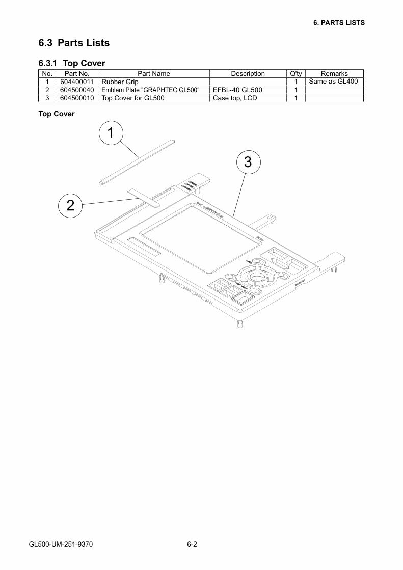
6.3.1 Top CoverNo. Part No. Part Name Description Q'ty Remarks1 604400011 Rubber Grip 1 Same as GL4002 604500040 Emblem Plate "GRAPHTEC GL500" EFBL-40 GL500 13 604500010 Top Cover for GL500 Case top, LCD 1
Top Cover
1
3
2
GL500-UM-251-9370 6-3
6. PARTS LISTS
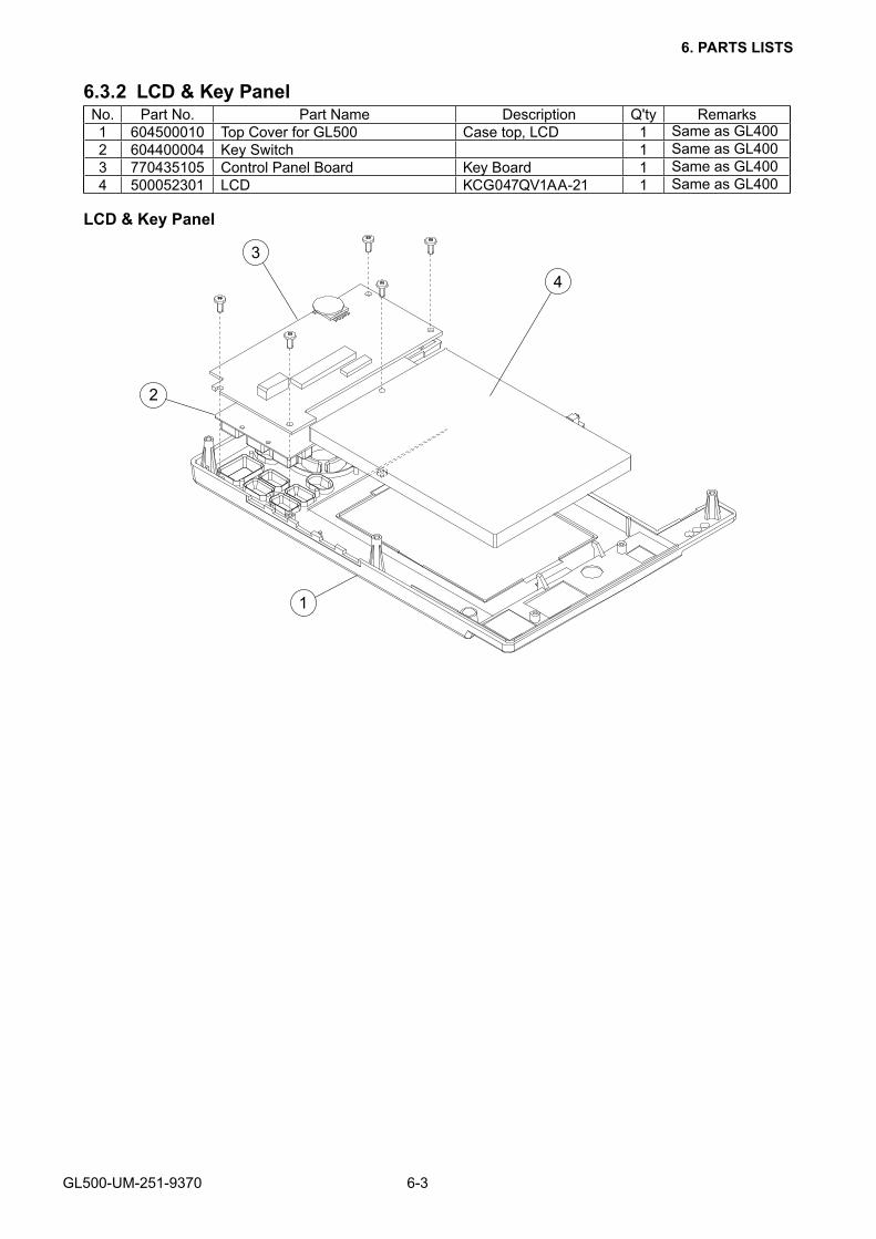
6.3.2 LCD & Key PanelNo. Part No. Part Name Description Q'ty Remarks1 604500010 Top Cover for GL500 Case top, LCD 1 Same as GL4002 604400004 Key Switch 1 Same as GL4003 770435105 Control Panel Board Key Board 1 Same as GL4004 500052301 LCD KCG047QV1AA-21 1 Same as GL400
LCD & Key Panel
1
2
3
4

GL500-UM-251-9370 6-4
6. PARTS LISTS
6.3.3 Top Cover, Reverse SideNo. Part No. Part Name Description Q'ty Remarks1 690440031 Cable, GL400-03A 1 Same as GL4002 690440040 Cable, GL400-04 1 Same as GL4003 500052325 Inverter, CXA-K0505-VJL 1 Same as GL4004 690440020 Flexible Cable, GL400-02 1 Same as GL4005 604400070 Inverter Insulating Sheet 1 Same as GL4006 604400060 LCD Insulating Sheet 1 Same as GL400
Top Cover, Reverse Side
1
1 6
5
2
4
4
9 3
GL500-UM-251-9370 6-5
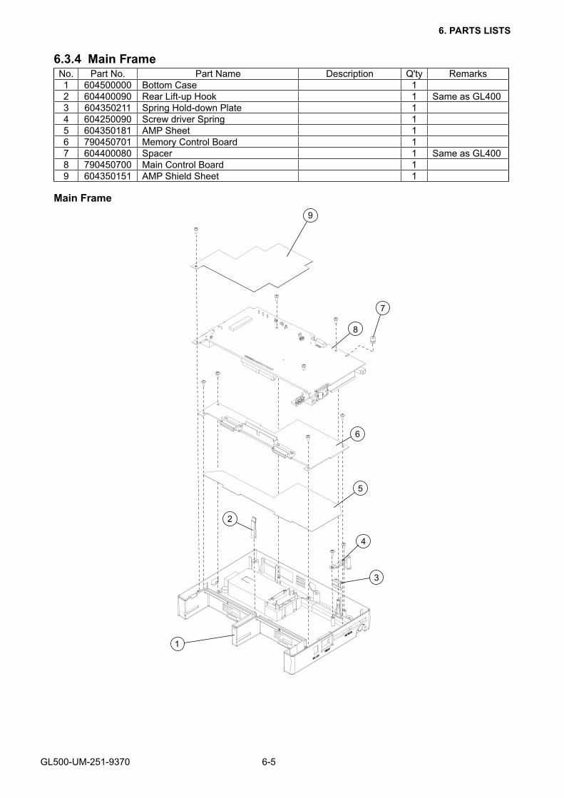
6. PARTS LISTS
6.3.4 Main FrameNo. Part No. Part Name Description Q'ty Remarks1 604500000 Bottom Case 12 604400090 Rear Lift-up Hook 1 Same as GL4003 604350211 Spring Hold-down Plate 14 604250090 Screw driver Spring 15 604350181 AMP Sheet 16 790450701 Memory Control Board 17 604400080 Spacer 1 Same as GL4008 790450700 Main Control Board 19 604350151 AMP Shield Sheet 1
Main Frame
1
2
3
4
5
6
8
7
9

GL500-UM-251-9370 6-6
6. PARTS LISTS
6.3.5 Bottom CaseNo. Part No. Part Name Description Q'ty Remarks1 604500020 Battery Cover 12 305820001 Screwdriver NDV-4 13 054025740 Serial Number Label 14 604500000 Bottom Case 15 795450001 4 VF-AMP Input Terminal Unit 1 or 2
795450002 4 MF-AMP Input Terminal Unit 1 or 2795450003 8 MS-AMP Input Terminal Unit 1 or 2
6 604500030 Model Name Label GL500 17 604350801 Caution Label 18 604500050 Warning Label 2 19 604350002 Input Terminal Unit Cover 1
Bottom Case
2
8
4
9
5
6
7
31

GL500-UM-251-9370 6-7
6. PARTS LISTS
6.3.6 Input Terminal UnitNo. Part No. Part Name Description Q'ty Remarks1 795450001 4 VF-AMP Input Terminal Unit 1 or 22 795450002 4 MF-AMP Input Terminal Unit 1 or 23 795450003 8 MS-AMP Input Terminal Unit 1 or 2
4 VF Amp Input Terminal Unit
4 MF Amp Input Terminal Unit
8 MS Amp Input Terminal Unit

GL500-UM-251-9370 7-1
7. BLOCK DIAGRAMS
7. BLOCK DIAGRAMS
PO
WE
RS
WS
W
J7
J11
J4 J4
To
KE
Y B
oard
To
Mem
ory
Con
trol
Boa
rd
Mai
n C
ontr
ol B
oard
(GL5
00-0
1*)
AC
Ada
pter
AC
IN
Prim
ary
circ
uit
Prim
ary
circ
uit
Sig
nal
inpu
tci
rcui
t
ISO
LAT
ING
: Con
nect
or to
Con
nect
or
1. 2.
ISO
LAT
ING
Sec
onda
ry c
ircui
t
Sec
onda
ryci
rcui
t
Mai
n U
nit P
ower
Blo
ck&
Mai
n C
ontr
ol B
lock
(N
o.1)
SA
45-3
229
NO
TE
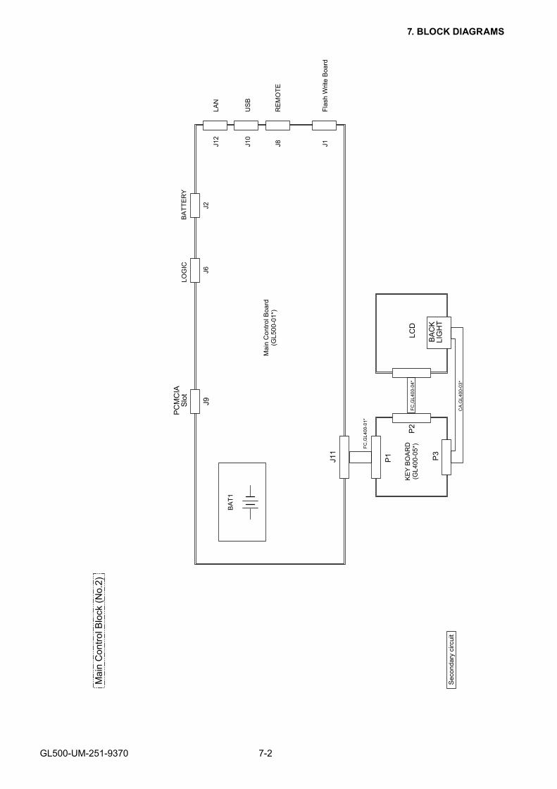
GL500-UM-251-9370 7-2
7. BLOCK DIAGRAMS
J9
PC
MC
IAS
lot
J11
LCD
P3
P2
P1
FC
,GL4
00-0
4*
FC
,GL4
00-0
1*
CA
,GL4
00-0
3*
BA
CK
LIG
HT
Mai
n C
ontr
ol B
oard
(GL5
00-0
1*)
LOG
ICB
AT
TE
RY
J6J2
J12
J10
J8
LAN
US
B
RE
MO
TE
J1F
lash
Writ
e B
oard
BA
T1
KE
Y B
OA
RD
(GL4
00-0
5*)
Sec
onda
ry c
ircui
t
Mai
n C
ontr
ol B
lock
(N
o.2)

GL500-UM-251-9370 7-3
7. BLOCK DIAGRAMS
J301 J3
03
J302
4ch
3ch
2ch
1ch
M-A
mp-
D B
oard
(GL5
00-0
8*)
J201
J202
Am
p-C
Boa
rd(G
L500
-05*
)
Sec
onda
ryci
rcui
t
Sig
nal I
nput
circ
uit
Sig
nal I
nput
circ
uit
Sig
nal I
nput
circ
uit
Sig
nal I
nput
circ
uit
J2
J4
J4
J1
J1
J101
J102
J201
J202
J301
J303
J302
J304
J305
4ch
3ch
BN
C
BN
C
2ch
1ch
BN
C
BN
C
Mem
ory
Con
trol
Boa
rd(G
L500
-02*
)
Am
p-C
Boa
rd(G
L500
-05*
)A
mp-
B B
oard
(GL5
00-0
4*)
Am
p-A
Boa
rd(G
L500
-03*
)V
-Am
p-D
Boa
rd(G
L500
-07*
)
Sec
onda
ryci
rcui
tS
econ
dary
circ
uit
J101
J102
Am
p-B
Boa
rd(G
L500
-04*
)
Sec
onda
ryci
rcui
tS
econ
dary
circ
uit
Sec
onda
ry c
ircui
t
To M
ain
Con
trol B
oard
(GL5
00-0
1*)
J2
J2
J1
Am
p-A
Boa
rd(G
L500
-03*
)
Sec
onda
ryci
rcui
t
Sig
nal I
nput
circ
uit
Sig
nal I
nput
circ
uit
Sig
nal I
nput
circ
uit
Sig
nal I
nput
circ
uit
Sig
nal I
nput
circ
uit
AM
P U
nit B
lock
4VF
AM
P4M
F A
MP

GL500-UM-251-9370 7-4
7. BLOCK DIAGRAMS
M-A
mp-
D B
oard
(GL5
00-0
8*)
AC
Ada
pter
+ -B
NC
+ -
+ - + -
BN
C
Mem
ory
Con
trol
Boa
rd(G
L500
-02*
)
Am
p-C
Boa
rd(G
L500
-05*
)
Am
p-B
Boa
rd(G
L500
-04*
)
V-A
mp-
D B
oard
(GL5
00-0
7*)
Pho
to M
OS
RE
LAY
Con
stan
t cur
rent
Atte
nuat
orS
elec
tor
Sel
ecto
r
A/D
AM
P
AM
PA
MP
AM
P
DC
±15
DC
±5V
DC
±5V
DC
+24V
Isol
atin
g
Isol
atin
g
Isol
atin
g
Isol
atin
g
DC
/DC
NM
A05
15D
DC
/DC
MK
D1R
5-05
12
Sec
onda
ry c
ircui
t
Mai
n C
ontro
l Boa
rd(G
L500
-01*
)
Am
p-A
Boa
rd(G
L500
-03*
)
Am
p-B
Boa
rd(G
L500
-04*
)
Sel
ecto
r
Sel
ecto
r
A/D
AM
PA
MP
AM
P
AM
P
DC
±5V
Am
p-A
Boa
rd(G
L500
-03*
)
Sig
nal I
nput
circ
uit
Sig
nal
Inpu
t
Sig
nal
Inpu
t
Tem
pera
ture
Sen
sor
Dec
oder
Am
p-C
Boa
rd(G
L500
-05*
)
Pho
to M
OS
RE
LAY
Con
stan
t cur
rent
Atte
nuat
or
AM
P DC
±15
Isol
atin
g
DC
/DC
NM
A05
15D
Dec
oder
AM
P B
lock
Det
ails
Recommended
![PP 451207100087 PUBLISHED BY AUTHORITY ISSN 0155-9370 · Queensland Government Gazette PP 451207100087 PUBLISHED BY AUTHORITY ISSN 0155-9370 Vol. 355] Friday 12 November 2010 VACANCIES](https://img.pdfslide.net/doc/110x75/5d5e708388c993ab568ba181/pp-451207100087-published-by-authority-issn-0155-9370-queensland-government.jpg)