Nanofabrication and Electrochemical Characterization of
Self-assembled Monolayers sandwiched between Metal
Nanoparticles and Electrode Surfaces
Pilar Cea*a,b, Santiago Martína,c, Alejandro González-Oriveb, Henrry M. Osorioa,b, Pablo
Quintína,b, Lucía Herrera,b 5
a. Departamento de Química-Física. Universidad de Zaragoza. Spain.
b. Instituto de Nanociencia de Aragón. Laboratorio de Microscopías Avanzadas.
Universidad de Zaragoza. Spain.
c. Instituto de Ciencia de los Materiales de Aragón. Universidad de Zaragoza-CSIC. 10
Spain.

ABSTRACT
Nanoscience and nanotechnology have reached the syllabi of many upper-division
undergraduate and master-level courses all over the world. There is therefore a growing 15
need for practical exercises that illustrate the fabrication, characterization, properties
and applications of nanomaterials. Here we describe an advanced-level laboratory
experiment in which students had the opportunity to fabricate surfaces modified by
ordered monolayers and nanostructured materials. The surface modification was
quantified by means of a quartz crystal microbalance, whilst the electrochemical 20
properties of the nanoarchitectures were assessed using cyclic voltammetry
experiments. Electron transfer across self-assembled monolayers mediated by gold
nanoparticles was presented as a topic for discussion, and consideration of potential
practical applications of the observed phenomena (catalytic and electrocatalytic
processes as well as development of optical, (opto)electronic and photovoltaic devices 25
with enhanced properties) was proposed as a further reading exercise.
ABSTRACT GRAPHIC
KEYWORDS
Upper-Division Undergraduate, Graduate Education/Research, Multidisciplinary, Hands 30
on learning, Materials Science

PEDAGOGICAL GOALS
Nanoscience and nanomaterials have found, or been proposed for, applications in many 35
important fields including health, electronics, energy production and storage,
purification and environmental cleanup applications, as well as industrial uses (foods,
textiles, cosmetics, sports, coatings aerospace and vehicle technologies, catalysis,
construction materials, military technology, etc.). This opens the need for designing new
laboratory demonstrations1 that can illustrate the phenomena occurring at the 40
nanoscale.2-7 In this practical exercise, students were guided through several aspects of
nanoscience, illustrated through a variety of surface modifications and manipulations.
Specifically, the experiment exposed students to the following concepts and skills:
(i) The key concept of ‘bottom-up’ assembly, illustrated through the formation
of a monolayer by means of the self-assembly method. 45
(ii) Determination of the surface coverage using a quartz crystal microbalance.
(iii) Synthesis of gold nanoparticles by reduction of a metal precursor.
(iv) Immobilize gold nanoparticles onto a thiol terminated monolayer.
(v) The effects of surface coverage illustrated through the cyclic voltammetry
response of a redox probe in a bare gold electrode, a gold electrode covered 50
by a tightly-packed monolayer and a gold nanoparticle/organic
monolayer/gold sandwich structure.
(vi) The potential applications of the fabricated devices.
EXPERIMENTAL OVERVIEW 55
A detailed student handout and the instructor notes for this laboratory experiment
are provided in the Supporting Information. Scheme II in the Supporting Information

summarizes the set of experiments of this practical. The practical was designed to be
completed over three laboratory sessions (three hours each), in groups of four or five
individuals. A chronogram of the activities carried out is presented in the Supporting 60
Information. The students prepared self-assembled monolayers (SAMs) of a dithiol
compound, whose surface coverage was determined by means of a Quartz Crystal
Microbalance (QCM). Cyclic voltammetry (CV) experiments demonstrated that the SAM
blocked the electron transfer at the electrode. Subsequently, gold nanoparticles (GNPs)
were synthetized and deposited onto the SAM surface, which was also quantified by 65
QCM. CV experiments demonstrated that the electron transfer was restored in the
GNPs/SAM/gold devices.
HAZARDS
This practical required the use of ethanol which is a volatile and flammable solvent. 70
Gold(III) chloride hydrate may cause irritation to the skin, eyes, and respiratory tract,
and may be harmful if swallowed or inhaled. Sodium borohydride is a toxic, flammable
compound and is also a source of basic borate salt, which can be corrosive. There is a
flammability hazard associated with the production of hydrogen from the reaction
between gold(III) and sodium borohydride. The reaction was performed in a fume hood. 75
Appropriate personal protection equipment (PPE) (gloves, safety glasses or goggles,
laboratory coats, covered shoes, etc.) was worn when handling chemical reagents.
EXPERIMENTAL SECTION
Reagents and Equipment
80
All materials are commercially available and were used as received: biphenyl-4,4′-
dithiol (95%) and gold(III) chloride hydrate(~52% Au basis) were purchased from
Aldrich; hexaammineruthenium(III) chloride (ACS reagent, 98%) and potassium chloride

(puriss. p.a. ≥ 99.5%) were provided by Sigma and Fluka, respectively. Gold electrodes
on glass for the CV studies were purchased from Arrandee™. Substrates for the QCM 85
experiments were purchased from Stanford Research (AT-cut, -quartz crystals with a
resonant frequency of 5 MHz having circular gold electrodes patterned on both sides).
QCM measurements were carried out using a Stanford Research system instrument.
CV experiments were done using a potentiostat from Eco Chemie and a standard three
electrode cell. 90
EXPERIMENTS AND RESULTS
Self-assembled films are spontaneously formed on surfaces by chemisorption of the
head group of an organic compound onto a substrate.8 Typical examples include thiols
on gold and trichlorosilanes on glass. The ease of preparation and the fact that it is 95
possible to fabricate SAMs on a variety of substrates using different terminal functional
groups have made the self-assembly technique a widely used ‘bottom-up’ method of
surface modification. For further details about SAMs see reference8 and the Supporting
Information. Quartz crystal microbalances determine the mass variation per unit area
by measuring the change in frequency of a quartz crystal resonator. The QCM can be 100
used under vacuum, in gas phase and in liquid environments. Therefore, it represents a
useful tool for the determination of the surface coverage of SAMs onto gold substrates.
More information about QCM fundamentals and experiments can be found in reference9
and in the Supporting Information.
Prior to the SAM formation the resonant frequency of a clean QCM substrate, f0, 105
was determined. Afterwards, a gold electrode from Arrandee™ for the electrochemical
experiments and a gold substrate from Standford Research for the QCM studies were
immersed in a 1 mM solution of biphenyl-4,4′-dithiol (Figure 1) in absolute ethanol, and
incubated at 20 ºC for 24 hours in the absence of light.

SHHS 110
Figure 1. Chemical structure of biphenyl-4,4′-dithiol.
Immersion of the gold electrodes in a biphenyl-4,4′-dithiol solution resulted in the
formation of a gold-thiolate monolayer according to:10
Au + HS-R-SH → Au-S-R-SH + ½ H2
The modified gold electrodes were rinsed thoroughly with absolute ethanol to remove 115
any physisorbed material and dried in nitrogen. Afterwards, the resonant frequency of
the modified QCM substrate was determined, f1 (see Scheme I.b in the Supporting
Information).The change in the frequency of oscillation ( f=f0-f1=20 Hz) was introduced
in the Sauerbrey equation:11
2/1q
2/1q
20
··A
m·f·2f (1) 120
where f0 is the fundamental resonant frequency, m is the mass change, A is the
electrode area, q is the density of the quartz (2.65 g·cm-3) and q is the shear module
(2.95·1011 dyn·cm-2). Figure 2 shows the QCM values at different incubation times. The
formation of the monolayer was completed after ca. 24 hours of incubation. The resulting
surface coverage for the biphenyl-4,4′-dithiol monolayer on gold was 6.1·10-10 mol·cm-2, 125
which is in good agreement with the theoretical value, 6.2·10-10 mol·cm-2, determined from
a molecular model (Spartan®08 V1.0.0).
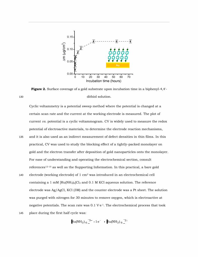
Figure 2. Surface coverage of a gold substrate upon incubation time in a biphenyl-4,4′-
dithiol solution. 130
Cyclic voltammetry is a potential sweep method where the potential is changed at a
certain scan rate and the current at the working electrode is measured. The plot of
current vs. potential is a cyclic voltammogram. CV is widely used to measure the redox
potential of electroactive materials, to determine the electrode reaction mechanisms,
and it is also used as an indirect measurement of defect densities in thin films. In this 135
practical, CV was used to study the blocking effect of a tightly-packed monolayer on
gold and the electron transfer after deposition of gold nanoparticles onto the monolayer.
For ease of understanding and operating the electrochemical section, consult
references12-15 as well as the Supporting Information. In this practical, a bare gold
electrode (working electrode) of 1 cm2 was introduced in an electrochemical cell 140
containing a 1 mM [Ru(NH3)6]Cl3 and 0.1 M KCl aqueous solution. The reference
electrode was Ag/AgCl, KCl (3M) and the counter electrode was a Pt sheet. The solution
was purged with nitrogen for 30 minutes to remove oxygen, which is electroactive at
negative potentials. The scan rate was 0.1 V·s-1. The electrochemical process that took
place during the first half cycle was: 145
26 3
3 6 3 )Ru(NHe 1)Ru(NH

The experiment was repeated using the SAM/gold electrode as the working electrode. It
is well-known that the deposition of a SAM of an organic material onto an electrode
leads to a diminution of the electron transfer to redox species in solution.2,16 This
phenomenon was clearly observed in the practical (Figure 3). Thus, the lack of Faradaic 150
current confirmed that the SAM was tightly-packed, essentially pinhole free2 and
effectively blocked electron transfer between the redox probe and the electrode surface.
Figure 3. Cyclic voltammograms obtained using a bare gold electrode (black), a gold
electrode covered by a biphenyl-4,4′-dithiol SAM (blue), and the SAM covered by GNPs 155
(red) as working electrodes.
A dispersion of gold nanoparticles (GNPs) was prepared by adding rapidly dropwise
0.5 mL of a 10-3 M NaBH4 (freshly prepared) aqueous solution to 30 mL of a 10-5 M
HAuCl4 aqueous solution with vigorous stirring at 2 °C using an ice-water bath. The 160
hydrodynamic diameter of these GNPs was in the 7-28 nm range.17 Incubation of the

SAM/gold substrate in the dispersion of GNPs (at 2 ºC) started 15 min after the mixture
of the reactants. Figure 4 shows the mass change obtained with the QCM versus the
incubation time (each point was determined after the substrate was withdrawn from the
incubation solution, rinsed with water and dried with nitrogen). An incubation time of 165
100 min into the GNPs dispersion led to a maximum surface coverage (Figure 4).
Figure 4. Deposited mass of GNPs vs. incubation time.
Incubation of the SAM/gold devices in a GPNs dispersion did not affect the integrity 170
of the SAM as demonstrated through experiments in the Supporting Information. After
the deposition of the GNPs on the SAM surface, the cyclic voltammogram (Figure 3)
exhibited a quasi-reversible behavior with a cathodic-anodic peak separation of 77 mV as
well as a near unity peak current ratio as observed for a bare gold electrode under the
same conditions. As previously reported, the deposition of conducting nanostructures 175
onto modified electrodes – made of insulating organic layers that completely block the
electron transfer when immersed in a redox probe – results in a restoration of the
Faradaic current18 in systems where disruption of the SAM by penetration of the
conducting nanostructures through the layer is ruled out by experimental evidence.19
This effect has been observed for several types of conducting nanostructures including 180

metal nanoparticles,19 carbon nanotubes,20 graphene sheets,21 quantum dots22 and even
purely molecular objects containing a large number of redox centers.23 This restoration of
the electron transfer has been attributed to a relay station effect of the conducting
nanostructures that facilitates the electronic coupling between the underlying electrode
and the redox probe.24 Therefore, when the conducting nanostructure is attached to the 185
SAM-modified electrode, the electron transfer process involves two consecutive steps: (i)
electron transfer between the underlying electrode and the conducting nanostructures,
mediated by electron tunneling through the organic layer, and (ii) electron transfer
between the conducting nanostructures and the redox probe, which is the rate-limiting
step with regard to charge transfer within these particular systems. 190
EVALUATION AND ASSESSMENT
The students were asked to answer specific questions prior to the experiment to ensure
their understanding of the fundamentals behind this practical (Supporting Information). 195
Through the anwers to these questions the students were expected to attain and
demonstrate a strong understanding of the nanofabrication and nanocharacterization
methods involved in this practical. Before the commencement of the laboratory sessions
students were invited to undertake further reading (Supporting Information) and after
completion of the practical entered into a class debate on the potential applications of 200
these nanostructures. In our classes, the instructor initiated the debate by asking why
GNP/SAM/electrode devices could have interest or applications beyond a conventional
electrode. The students in our cohort indicated the different properties of nano-sized gold
from the bulk counterpart and also noted that GNPs exhibit a high electrocatalytic
activity, which may result in electrocatalytical applications. A significant number of 205
students also highlighted the possibility of forming arrays of electrodes in which each

electrode is as small as a few nanometers resulting in a higher sensitivity and selectivity,
i.e, sensor applications including biosensors and immunosensors. Some students
remarked that the passivating organic layer may result in electrodes with a low
background capacitance which facilitates low detection limits in electroanalysis. Students 210
also mentioned potential applications in the field of photovoltaics due to the high density
of states that can exist on the nanoparticles and also the fact that the energy levels of the
nanoparticles are tuneable by altering their size.
Assessment of student understanding of associated concepts was achieved by the 215
laboratory report that students were asked to prepare (Supporting Information). Nearly all
students showed a strong grasp on the experiments involved and a good understanding
of the practical.
CONCLUSIONS 220
This demonstration tied together several nanofabrication and characterization
techniques and the observation of new phenomena and properties of materials at the
nanoscale. Ultimately, we expect that this comprehensive activity, which builds on the
excitement of creating conducting nanostructures with important optical, electronic and
catalytic applications, will stimulate interest in nanoscience and nanotechnology and 225
contribute to inspire students to pursue careers in these fields.
ASSOCIATED CONTENT
Supporting Information
Experimental handout for the students and notes for the instructor are included in 230
the Supporting Information. This material is available via the Internet at
http://pubs.acs.org.

AUTHOR INFORMATION
Corresponding Author
*E-mail: [email protected] 235
ACKNOWLEDGMENTS
We thank students in the Master in Nanostructured Materials for Nanotechnology
Applications from Zaragoza University for providing feedback for the improvement of
this practical as well as Prof. P. J. Low from the University of Western Australia for 240
useful discussions. Financial support from the Department of Physical Chemistry,
DGA/Fondos Feder , CTQ2012-33198 and CTQ2013-50187-EXP grants is also
acknowledge.
REFERENCES 245
(1) Jones, M. G.; Blonder, R.; Gardner, G. E.; Albe, V.; Falvo, M.; Chevrier, J. Nanotechnology and Nanoscale Science: Educational challenges. International Journal of Science Education 2013, 35, 1490-1512.
(2) Cea, P.; Lopez, M. C.; Martin, S.; Villares, A.; Pera, G.; Giner, I. The use of cyclic
voltammetry to probe the passivation of electrode surfaces by well-ordered self-250
assembly and Langmuir-Blodgett films. J. Chem. Edu. 2009, 86, 723-725.
(3) Gottfried, D. S. Review of nanotechnology in undergraduate education. J. Chem. Edu. 2012, 88, 544-545.
(4) Rushton, G. T.; Criswell, B. A. Cutting-edge and cross-cutting: connecting the dots between nanotechnology and high school chemistry. J. Chem. Edu. 2012, 89, 255
1217-1219.
(5) Sekiya, M.; An, A.; Ata, M. Nanocommunication design in graduate-level education and research training programs at Osaka University. J. Nanopart. Res. 2014, 16:2595.
(6) Jones, A. R.; Anderson, A. A.; Yeo, S. K.; Greenberg, A. E.; Brossard, D.; Moore, J. 260
W. Using a deliberative exercise to foster public engagement in nanotechnology. J. Chem. Edu. 2014, 91, 179-187.
(7) Bishop, L. M.; Tillman, A. S.; Geiger, F. M.; Haynes, C. L.; Klaper, R. D.; Murphy,
C. J.; Orr, G.; Pedersen, J. A.; DeStefano, L.; Hamers, R. J. Enhancing graduate
student communication to general audiences through blogging about 265
nanotechnology and sustainability. J. Chem. Edu. 2014, 91, 1600-1605.
(8) Ulman, A. An Introduction to Ultrathin Organic Films: From Langmuir-Blodgett to Self-Assembly; Academic Press, Inc.: San Diego, 1991.
(9) Xie, Q.; Li, Z.; Deng, C.; Liu, M.; Zhang, Y.; Ma, M.; Xia, S.; Xiao, X.; Yin, D.; Yao,
S. Electrochemical quartz crystal microbalance monitoring of the cyclic 270

voltammetric deposition of polyaniline - A laboratory experiments for undergraduates. J. Chem. Edu. 2007, 84, 681-684.
(10) Karpovich, D. S.; Blanchard, G. J. An undergraduate laboratory experiment for the direct measurement of monolayer-formation kinetics. J. Chem. Edu. 1995, 72,
466-470. 275
(11) Sauerbrey, G. The use of quartz oscillators for weighing thin layers and for microweighing. Z. Physik 1959, 155, 206-222.
(12) Kissinger, P. T.; Heineman, W. R. Cyclic voltammetry. J. Chem. Edu. 1983, 60,
702-706. (13) Mabbott, G. A. An introduction to cyclic voltammetry. J. Chem. Edu. 1983, 60, 280
697-702. (14) Van Benschoten, J. J.; Lewis, J. Y.; Heineman, W. R.; Roston, D. A.; Kissinger, P.
T. Cyclic voltammetry experiment. J. Chem. Edu. 1983, 60, 772-776.
(15) Bard, A.; Faulkner, L. R. Electrochemical Methods New York, 1980.
(16) Porter, M. D.; Bright, T. B.; Allara, D. L. Spontaneously organized molecular 285
assemblies. 4. Structural characterization of normal-alkyl thiol monolayers on gold by optical ellipsometry, infrared-spectrsocopy, and electrochemistry. J. Am. Chem. Soc. 1987, 109, 3559-3568.
(17) Osorio, H. M.; Cea, P.; Ballesteros, L. M.; Gascon, I.; Marqués-González, S.;
Nichols, R. J.; Pérez-Murano, F.; Low, P. J.; Martín, S. Preparation of nascent 290
molecular electronic devices from gold nanoparticles and terminal alkyne functionalised monolayer films. J. Mater. Chem. C. 2014, 2, 7348-7355.
(18) Bethell, D.; Brust, M.; Schiffrin, D. J.; Kiely, C. From monolayers to nanostructured materials: an organic chemist's view of self-assembly. J. Electroanal. Chem. 1996, 409, 137-143. 295
(19) Zhao, J.; Wasem, M.; Bradbury, C. R.; Fermin, D. J. Charge transfer accross self-assembled nanoscale metal-insulator-metal heterostructures. J. Phys. Chem. C. 2008, 112, 7284-7289.
(20) Chou, A.; Eggers, P. K.; Paddon-Row, M. N.; Gooding, J. J. Self-assembled carbon
nanotube electrode arrays: effect of length of the linker between nanotubes and 300
electrode. J. Phys. Chem. C 2009, 113, 3203-3211.
(21) Xie, X.; Zhao, K.; Xu, X.; Zhao, W.; Liu, S. X.; Zhu, Z.; Li, M.; Shi, Z.; Shao, Y. Study of heterogeneous electron transfer on the graphene/self-assembled monolayer modified gold electrode by electrochemical approaches. J. Phys. Chem. C. 2010, 114, 1423-14250. 305
(22) Kantor-Uriel, N.; Roy, P.; Saris, S.; Kiran, V.; Waldeck, D. H.; Naaman, R.
Evidence for enhanced electron transfer by multiple contacts between self-assembled organic monolayers and semiconductor nanoparticles. J. Phys. Chem. C. 2015, 119, 15839-15845.
(23) Lhenry, S.; Jalkh, J.; Leroux, Y. R.; Ruiz, J.; Ciganda, R.; Astruc, D.; Hapiot, P. 310
Tunneling dendrimers. Enhancing charge transport through insulating layer using redox molecular objects. J. Am. Chem. Soc. 2014, 136, 17950-17953.
(24) Chazalviel, J.-N.; Allongue, P. On the origin of the efficient nanoparticle mediated electron transfer across a self-assembled monolayer. J. Am. Chem. Soc. 2011,
133, 762-764. 315
Recommended