ORDER NO.
CRT2916
GX470AUDIO SYSTEMHEAD UNIT
CRT2916
PUB.NO.
Manufactured for TOYOTA
by PIONEER CORPORATION
VEHICLE DESTINATIONPRODUCED
AFTERTOYOTA PARTS No. ID No.
PIONEER MODEL No.
LEXUS GX470 U.S.A., CANADA November 2002 86120-60440 P1731 KEX-M8727ZT/UCKEX-M8727ZT-91/UC
LEXUS GX470 U.S.A., CANADA November 2002 86120-60470 P1732 KEX-M8527ZT/UCKEX-M8527ZT-91/UC

1 2 3 4
C
D
F
A
B
E
813
4
LER
BU
Q
05
Q
44
AM
PW
IC401
JM2068M
MIXING
MB
AMB
KEX-M8727ZT/UC10
3. BLOCK DIAGRAM AND SCHEMATIC DIAGRAM3.1 BLOCK DIAGRAM
CN501
ANT
IC561HA12181FP
16 3
9
S-80735ANDZIIC602
2
1
RESET
VDD
Q811Q
Q816
ILLB
FML
CN804
5,613,14
13 15
12RESET
XIN
XO
UT
SYSTEM CONTROL
IC601
KDT,kst
A MAIN UNITFM/AM TUNER UNIT
KEYBOARD UNITB
51
LOC
L
53
PC
E2
33
pc
k
52
PC
E1
93
SL
56
FMS
D
57
st
31,32
PD
O,P
DI
IC 3EEPROM
28
27
FM/AM 1ST IF 10.7MHzT51 Q51 CF51 CF52 CF53
IC1MIXER, IF AMP, DET.
6
21COMP
2225 10 14 12 15 16 8 13 2 4
CF202
VD
D
VC
C
DI/D
O
CE
2
CK
CE
1
SD
BW
SL
FMS
D
NL2
IC 2 FM MPX
AMANT
FMANT
ATT
ATT
AMRF
FMRF
IMG ADJ
RF ADJ
X90110.25MHz
ANT ADJ
LOCL
AMDETMPXREF 41kHz
AM 2ND IF450kHz
1
ST
IND
L ch
9A
MD
ET
17
AM
PN
S
26 RFGND
CN901
KEY MATRIX
ILLUMINATION
2
Q502
AUD+BSW5V
Q4
Q252
55
NL2
Q406
N
RBDSDECODER
TUNER
AM PNS
FML
AML
Q561
A
IC501LA1061M
1
135
6
Q501NIN
MFIX
SUB
MAIN
SUB
MAIN
PD5840A
CN251CN252
CN253CN255
CN256
CN254
IC251HA12216F
TAPE EQUALIZER
MECHANISM DRIVERIC351
PA2020A
Q271
BU
MSUB
MOTOR
MMAINMOTOR
7
+B
TAPE-L
MTL
MTL
VR302
VREF
6
16
111228
37
39
17
5
2
NR
1
ST
BY
LOA
D
LOADSWITCH
MODESENSE
1
4
5
2
1
4
3
20
641
641
C DECK UNIT
D SENSOR UNIT
SWITCH70µs
19
CR
EQ
BU
CN3534
3
20
AUD+B
CSL
MS,DIR,PLAY,MTL,NR,CSLOAD,POS,ES,SC2,SC1,CM,STBY
3
NL1
91
NL1
18LDET
IC252PM4009A
8 20
19 ldet
RC
K,R
DT,
rd
slk
,57K
,dr
st
FWDLcH
REVLcH
1 2 3 4

5 6 7 8
C
D
F
A
B
E
Q816
CN804
5,6
SYSTEM C
IC
KDT,k
6
FMS
D
57
st
Q252
55
Q406
F
PD5
91
NL1
IC25PM40
20
KEX-M8727ZT/UC
Q811Q813
ILLB
NJM2068MDIC204
NJM2068MDIC203
L+
LANL+
L-
ANT
TX+
TX+
TX-
TX-
RSL-RSL+
TX1-
TX1+
LANL
2
5
5
7 5
8
Q808
Q802
ILLACC
HA12187FPIC701
S-81256SGUP-DIMIC870
4
LAM
P
1
SY
SP
WR
ONTROLLER
AVC-LAN601
73
2
SWVDD
AUD+B
AUD+B
AUD+B
ASENS
BSENS
st
6
SY
SM
UT
E1
5
SY
SM
UT
E2
RX
TX
IPPW22
30
29
8 6
1
2
CN801
CN473BU
ISENS
+B
+B
43
FMP
W
TC4052BFIC202
2 TC4052BFIC302
NJM2068MDIC201
BU
7
NJM2068MDIC304
Q205Q204
NJM2068MDIC303
16 8 8
16 82
8
CN472
Q305Q304
Q867Q865
Q866Q864
Q860
Q861
Q862
Q863
BU
BU
3
Q563
Q405
Q564
44
AM
PW
NL2
IC401
NJM2068MD
ACC
Q807
Q870
Q645
Q644
ASEN
ACC
Q805
ISENILL
11SWVDD
100ANTB
5
3 2
75
Q806
BSENBU
BU
BU
VDD
VDD
AMP
AUD+B
SW5V
Q453
Q451
Q452
Q882BU
Q884
AUDIO SELECT FOR AMP
AUDIO SELECT FOR RSA
TUNER MIXING AMP UNBALANCE TO BALANCE
UNBALANCE TO BALANCE
BALANCE TO UNBALANCE
SYSTEM MUTE
SYSTEM MUTE
5R6V IC
16763
7676
ML
AML
6
LANL-
LANL+
LANL-
CSL
TUL
LANL
TUL
CSL
FMBAMB
FMB
AMB
SWVDD
840A
1
1209A
RC
K,R
DT,
rd
slk
,57K
,dr
st
115 6 7 8

1 2 3 4
C
D
F
A
B
E
TUNER
5V
KEXKEX
KEX-M8727ZT/UC12
3.2 OVERALL CONNECTION DIAGRAM(GUIDE PAGE)
A-a A-b
A-a A-b
A-b A-a
Large sizeSCH diagram
Guide page
Detailed page
Note: When ordering service parts, be sure to refer to " EXPLODED VIEWS AND PARTS LIST" or "ELECTRICAL PARTS LIST".
A-a
A
B CN901
C CN251
RBDS DECODER
FM:-24.0dBs(30%,400Hz)AM:-11.7dBs(30%,400Hz)
TAPE:-7.5dBs(0dB,1kHz)
SYSTEM CONTROLLER
8V
FM DIVERSITY
1 2 3 4

5 6 7 8
C
D
F
A
B
E
A-a A-b
A-a A-b
A-b A-a
KEX-M8727ZT/UC
A-b
A
A MAIN UNIT
Decimal points for resistorand capacitor fixed valuesare expressed as :2.2 2R20.022 R022
← ←
The > mark found on some component parts indicatesthe importance of the safety factor of the part.Therefore, when replacing, be sure to use parts ofidentical designation.
Symbol indicates a resistor.No differentiation is made between chip resistors anddiscrete resistors.
NOTE :
Symbol indicates a capacitor.No differentiation is made between chip capacitors anddiscrete capacitors.
FM:-14.4dBsAM:-14.8dBs(KEX-M8727ZT)
AM:-11.5dBs(KEX-M8527ZT)
TAPE: -7.5dBs
L-
L+(AMP)
SYSTEM MUTE
R+
R-
L-
L+(RSA)
UNBALANCE TO BALANCE
SYSTEM MUTE
UNBALANCE TO BALANCE
AUDIO SELECTOR FOR RSA/RSE
FM:-14.4dBsAM:-14.8dBs(KEX-M8727ZT)AM:-11.5dBs(KEX-M8527ZT)
TAPE: -7.5dBs
VDD 5V
AUDIO SELECTORFOR AMP
BALANCE TO UNBALANCE
TUNER MIXING AMP
HARD MUTE
FM:-4.6dBsAM:-5.0dBs
(KEX-M8727ZT)AM:-1.7dBs
(KEX-M8527ZT)TAPE: +2.3dBs
>
13.2V 13.2V
ILLSENSE
B.UPSENSE
ACCSENSE
13.2V
13.2V
5V
8.3V
5V
R417,418 KEX-M8727ZT 91K KEX-M8527ZT 62K
135 6 7 8

1 2 3 4
C
D
F
A
B
E
KEX-M8727ZT/UC14
A-a
A-b
A-a
A-a
A-b 1 2
RB
DS
DE
CO
DE
R
TU
NE
R M
IXIN
G A
MP
FM:-
24.0
dB
s(30
%,4
00H
z)A
M:-
11.7
dB
s(30
%,4
00H
z)
5V
FM D
IVE
RS
ITY
KE
X-M
8727
ZT
KE
X-M
8527
ZT
1 2 3 4

5 6 7 8
C
D
F
A
B
E
KEX-M8727ZT/UC
A-a
A-b
A-a
A-a
A-b3 4 5 6 7
BC
N90
1
CC
N25
1TA
PE
:-7.
5dB
s(0d
B,1
kHz)
SYST
EM CO
NTRO
LLER
8V
5V
155 6 7 8

1 2 3 4
C
D
F
A
B
E
HA
RD
MU
TE
KEX-M8727ZT/UC16
A-a
A-b
A-b 1 2
AM
AIN
UN
IT
FM:-
14.4
dB
sA
M:-
14.8
dB
s(K
EX
-M87
27Z
T)
AM
:-11
.5d
Bs
(KE
X-M
8527
ZT
)TA
PE
: -7.
5dB
s
L- L+(A
MP
)
SY
ST
EM
MU
TE
R+ R-
L- L+(R
SA
)
UN
BA
LAN
CE
TO
BA
LAN
CE
SY
ST
EM
MU
TE
UN
BA
LAN
CE
TO
BA
LAN
CE
AU
DIO
S
ELE
CT
OR
FO
R R
SA
/RS
E
FM:-
14.4
dB
sA
M:-
14.8
dB
s(K
EX
-M87
27Z
T)
AM
:-11
.5d
Bs
(KE
X-M
8527
ZT
)TA
PE
: -7.
5dB
s
VD
D 5
V
AU
DIO
SE
LEC
TO
RFO
R A
MP
BA
LAN
CE
TO
UN
BA
LAN
CE
NG
AM
P
5V
R
417,
418
KE
X-M
8727
ZT
91K
KE
X-M
8527
ZT
62K
1 2 3 4

5 6 7 8
C
D
F
A
B
E
KEX-M8727ZT/UC
A-a
A-b
A-b3 4 5 6 7
Dec
imal
po
ints
fo
r re
sist
or
and
cap
acit
or
fixe
d v
alu
esar
e ex
pre
ssed
as
:2.
2
2R2
0.02
2
R02
2
←
←
Th
e >
mar
k fo
un
d o
n s
om
e co
mp
on
ent
par
ts in
dic
ates
the
imp
ort
ance
of
the
safe
ty f
acto
r o
f th
e p
art.
Th
eref
ore
, wh
en r
epla
cin
g, b
e su
re t
o u
se p
arts
of
iden
tica
l des
ign
atio
n.
Sym
bo
l in
dic
ates
a r
esis
tor.
No
dif
fere
nti
atio
n is
mad
e b
etw
een
ch
ip r
esis
tors
an
dd
iscr
ete
resi
sto
rs.
NO
TE
: Sym
bo
l in
dic
ates
a c
apac
ito
r.N
o d
iffe
ren
tiat
ion
is m
ade
bet
wee
n c
hip
cap
acit
ors
an
dd
iscr
ete
cap
acit
ors
.
HA
RD
MU
TE
FM:-
4.6d
Bs
AM
:-5.
0dB
s(K
EX
-M87
27Z
T)
AM
:-1.
7dB
s(K
EX
-M85
27Z
T)
TAP
E: +
2.3d
Bs
>
13.2
V13
.2V
ILL
SE
NS
EB
.UP
SE
NS
EA
CC
SE
NS
E
13.2
V
13.2
V
5V
8.3V
5V
175 6 7 8

1 2 3 4
C
D
F
A
B
E
KEX-M8727ZT/UC18
3.3 KEYBOARD UNIT
B
PWR•VOL
A CN804
1 2 3 4

5 6 7 8
C
D
F
A
B
E
KEX-M8727ZT/UC
B
B KEYBOARD UNIT
8V 8
5mA
8V 8
5mA
8V 8
5mA
8V 8
5mA
8V 8
5mA
8V 8
5mA
195 6 7 8

1 2 3 4
C
D
F
A
B
E
C4
Q2712SC4116
KEX-M8727ZT/UC20
3.4 CASSETTE MECHANISM MODULE
C
DECK UNIT
MU
TE
HA12216F
11121314151617181920
40393837363534333231
30 29 28 27 26 25 24 23 22 21
1 2 3 4 5 6 7 8 9 10
R256
180
R291
0R0
C271
1/50
R283 0R0
R284 0R0
R282 0R0
C253 390P
C254 390P
C252 390P
C251 390P
R281 0R0
R255
180
C25
6
R01
R258
18K
R40
2
3R3K
R403 910
R32
2
0R0
R293
0R0
C272 R1
R28
7
0R0
R28
50R
0
HD1HEAD ASSYEXA1594
TEST TAPENCT-150(400Hz, 200nWb/m)
RL
RR
FR
FL
C30
2
R1
VR302
33K(B)
-8.24dBs(300mV)±1dB
Fwd-R
Fwd-L
Rev-R
Rev-L
NFI(L)
RIN(L)
RIP
FIN(L)
GND
GND
FIN(R)
VREF
RIN(R)
NFI(R)
M-O
UT
(R)
EQ
OU
T(R
)
TA
I(R
)
BIA
S
RA
I(R
)
PB
OU
T(R
)
DE
T(L
)
MU
TE
MSGV(R)
MAOUT
MSI
MSDET
MSGV
F/R
120/70
NR
MO
UT
(L)
EQ
OU
T(L
)
TA
I(L) NC
RA
I(L)
PB
OU
T(L
)
NC
DE
T(L
)
MS
GV
(S)
CN252
CN251
DOLBY B NR
IC251
VR301
33K(B)
C31
0
R1
C30
9
R1
R32
1
0R0
VCC
CCP1280
CCP1280
NC
MSOUT
NC
NC
R260
13K
R26
2
270K
C40
1
3900
P
R40
1
15K
R27
6
100K
C40
2
R33
C404 R01
C40
3
R02
2R
274
0R0
R273
0R0
R27
2
0R0
R292
0R0
R27
1
18K
C30
1
R1
R294
0R0
R259
13K
C25
5
R01
R257
18K
R26
1
270K
A
C
CN353
1 2 3 4

5 6 7 8
C
D
F
A
B
E
0
R32
1R
276
1
C40
3
R02
2R
274
CN353
KEX-M8727ZT/UC
C D
SENSOR UNIT
SWITCHES:SENSOR UNIT S101:LOAD SWITCH..........EJECT-PLAY S102:MODE SWITCH............ON-OFF S103:70µs SWITCH...............ON-OFFThe underlined indicates the switch position.
R275
47K
R35
11K
R35
21K
R35
31K
R35
41K
R373 0R0
R35
5
270K
C35
2
3900
P
R36
230
0
C35
1R
22
C35
3R
01
C35
4R
01
R374 0R0
C356 R01
C355 R1D35
21S
S35
5
M1 MOTOR UNIT(MAIN MOTOR)EXA1618
S101LOAD
ESG1007x3
S102MODE
Q101EGN1004
M2MOTOR UNIT(SUB MOTOR)EXA1623
RS3
RS2
RS1
SC2
SC1
TAB
MC
CE
VCC2
NC
VCC
MCS
RRS
FRS
RSB
C
TAB
MS2
NC
NC
MM
SM1
RSB
GND
RS
mtl
MCS
load
CN255CN253
CN256
CN254
MECHANISMDRIVER
IC35
1
PA
2020
A
0R0
R375 0R0
S10370µs
100K
0R0
R404
270K
C405 R033
R277
220K
R27
810
0K
Q2712SC4116
D
L101
L102
215 6 7 8
5 6 7 8
C
D
F
A
B
E
KEX-M8727ZT/UC
6. ADJUSTMENT6.1 CONNECTION DIAGRAM
H/U EMV(DENSO)
SDVD(PANA)
NAVI ECU(DENSO)
20P
12P20P 6P 10P 14P 8P
10P18P
20P
18P 10P
6P 10P 14P12P20P
20P
25P
8P
GGD1239
16P
16P
GGD1169
20P
25P
GGD1240
GGD1305
AUI+
AUI-
FR+
FR-
KEX-M8727ZT/UC
RSE-ECU
24P 10P 32P
20P 12P 16P
MCD
32P
Rear Display(F-TEN)
16P
16P
24P
20P
16P
16P
AV Unit
10P 32PGGD1306
CDX-M8027ZT/E
AMP(M/L)
32P
12P
GGD1304
24P12P
Bullet connector(To DC Regulated Power Supply)
Bullet connector(To DC Regulated Power Supply)
Bullet connector(To DC Regulated Power Supply)
Bullet connector(To DC Regulated Power Supply)
Bullet connector(To DC Regulated Power Supply)
Bullet connectorSP Line
1. RSE (option) system
355 6 7 8

1 2 3 4
C
D
F
A
B
E
KEX-M8727ZT/UC36
RSA Controller
24P
GGD1239
GGD1169
KEX-M8727ZT/UC
CDX-M8027ZT/E
H/U EMV(DENSO)
32P
12P20P 6P 10P 14P 8P
10P18P
32P
18P 10P
10P 14P12P20P
20P
25P
8P
16P
16P
20P
25P
GGD1240
AUI+AUI-
FR+ FR-
24P
GGD1302
MCD
NAVI ECU(DENSO)
6P
20P
AMP(M/L)
Bullet connector(To DC Regulated Power Supply)
Bullet connector(To DC Regulated Power Supply)
Bullet connector(To DC Regulated Power Supply)
Bullet connectorSP Line
*Please connect only one Multi CD at the same time*MCD does not operate if RSA controller is not connected.
2. RSA (option) system
1 2 3 4

5 6 7 8
C
D
F
A
B
E
KEX-M8727ZT/UC
GGD1239
GGD1169
KEX-M8727ZT/UC
CDX-M8027ZT/E
H/U EMV(DENSO)
32P
12P20P 6P 10P 14P 8P
10P18P
18P 10P
10P 14P20P
20P
25P
8P
16P
16P
20P
25P
GGD1240
AUI+AUI-
FR+ FR-
GGD1300
AMP(M/L)
MCD
NAVI ECU(DENSO)
GGD1304
32P
12P
24P
12P
Bullet connector(To DC Regulated Power Supply)
Bullet connector(To DC Regulated Power Supply)
Bullet connector(To DC Regulated Power Supply)
Bullet connector(To DC Regulated Power Supply)
Bullet connectorSP Line
*Please connect only one Multi CD at the same time
3. Standard system
375 6 7 8

1 2 3 4
C
D
F
A
B
E
KEX-M8727ZT/UC38
Bullet connectorSP Line
H/U EMV(DENSO)
SDVD(PANA)
NAVI ECU(DENSO)
20P
12P20P 6P 10P 14P 8P
10P18P
20P
18P 10P
6P 10P 14P12P20P
20P
25P
8P
GGD1239
16P
16P
GGD1169
20P
25P
GGD1240
GGD1305
AUI+
AUI-
FR+
FR-
KEX-M8527ZT/UC
GM-8027ZT/E
RSE-ECU
24P 10P 32P
20P 12P 16P
MCD
32P
Rear Display(F-TEN)
16P
16P
24P
20P
16P
16P
AV Unit
10P 32PGGD1306
CDX-M8027ZT/E
AMP
32P
12P
GGD130424P12P
Bullet connector(To DC Regulated Power Supply)
Bullet connector(To DC Regulated Power Supply)
Bullet connector(To DC Regulated Power Supply)
Bullet connector(To DC Regulated Power Supply)
Bullet connector(To DC Regulated Power Supply)
4. RSE (option) system
1 2 3 4

5 6 7 8
C
D
F
A
B
E
KEX-M8727ZT/UC
RSA Controller
24P
GGD1239
GGD1169
KEX-M8527ZT/UC
CDX-M8027ZT/E
GM-8027ZT/E
H/U EMV(DENSO)
32P
12P20P 6P 10P 14P 8P
10P18P
32P
18P 10P
10P 14P12P20P
20P
25P
8P
16P
16P
20P
25P
GGD1240
AUI+AUI-
FR+ FR-
24P
GGD1302
AMP
MCD
NAVI ECU(DENSO)
6P
20P
*Please connect only one Multi CD at the same time*MCD does not operate if RSA controller is not connected.
Bullet connectorSP Line
Bullet connector(To DC Regulated Power Supply)
Bullet connector(To DC Regulated Power Supply)
Bullet connector(To DC Regulated Power Supply)
5. RSA (option) system
395 6 7 8

1 2 3 4
C
D
F
A
B
E
KEX-M8727ZT/UC40
GGD1239
GGD1169
GGD1304
KEX-M8527ZT/UC
CDX-M8027ZT/E
GM-8027ZT/E
H/U EMV(DENSO)
32P
12P20P 6P 10P 14P 8P
10P18P
32P
18P 10P
10P 14P12P20P
20P
25P
8P
16P
16P
20P
25P
GGD1240
AUI+AUI-
FR+ FR-
GGD1300
AMP
MCD
NAVI ECU(DENSO)
24P
12P
Bullet connector(To DC Regulated Power Supply)
Bullet connector(To DC Regulated Power Supply)
Bullet connector(To DC Regulated Power Supply)
Bullet connector(To DC Regulated Power Supply)
Bullet connectorSP Line
*Please connect only one Multi CD at the same time
6. Standard system
1 2 3 4

5 6 7 8
C
D
F
A
B
E
KEX-M8727ZT/UC
6.2 TUNER/AUDIO ADJUSTMENT
DOLBY B NR ADJUSTMENTNo. Test Tape Adjustment Point Adjustment Method
(Switch Position)1 NCT-150 VR301(Lch),VR302(Rch) mV Meter : –8.24dBs(300mV)±1dB
(400Hz,200nwb/m) (DOLBY NR Switch : OFF)
VR302
mVMeter
VR301
L-CHR-CH
Pin2Pin3
CN251
DECK UNIT
Extention Cord GGD1121MAIN UNITCN353
415 6 7 8

1 2 3 4
C
D
F
A
B
E
KEX-M8727ZT/UC42
Connection:
Setting of the pulse generator (setting of
superimposed pulse)
Adjustment:
1. Setting of SSG
Percentage modulation : 30%Receiving frequency : 1,000 kHz
Modulation frequency : 400 Hz
Antenna input : 74 dBuV (EMF)
2. Tune a RADIO to the "1,000kHz" with 1' condition.
3. Mix signal with the above-mentioned pulse and
SSG' moduration OFF.
4. Variable resistance adjust noise level to a
minimam.
Adjustment point : VR561 (Main Unit)
Pulse generator(equivalent to HP8011A)
SSG
2-signal pad AM dummy
Output
Noise meter
Pulse width :50usec
Pulse intervals :5msec
Pulse voltage :4Vp-p
4Vp-p(EMF)
50us
5ms
AM NOISE CANCELER ADJUSTMENT
KEX-M8727ZT/UCKEX-M8527ZT/UC
1 2 3 4
5 6 7 8
C
D
F
A
B
E
KEX-M8727ZT/UC
6.3 SELF-DIAGNOSTIC FUNCTION
1.To Service Check
1. Press [AUDIO] key of EMV .2. Press [DISPLAY] key of EMV .3. The position of A and B is order of pushed 6 times in A,B,A,B,A and B. ->Service Check screen is displayed.
->As it is, it waits for a while. (In general less than 1 minute)
DISPLAY
Display
Frame of display adjustment
Audio mode
The name of each apparatus, such as an Audio H/U, is displayed.
B
A
2.Service Check
Service Check
EMV Audio H/U
DSP AMP
CD-CH
LAN Monitor
435 6 7 8

1 2 3 4
C
D
F
A
B
E
KEX-M8727ZT/UC44
3.How to exit from the diagnostic test mode
The diagnostic result of each model is displayed.Results are [OK], [NCON],[CHEK], and [EXCH].OK : No error codeNCON : EMV has judged it as the thing without connection. (Disconnection being possible if there is actually connection)CHEK : An error code indicating that diagnosis is judged to be necessary is entered.EXCH : An error code indicating that exchange is judged to be necessary is entered.
ACC-OFF
Unit Check Mode Audio H/U
Current Memory
61-40
Occurred Date/Time
When displayed as [CHEK] or [EXCH], details will be displayed if the portion is touched.
It changes on the screen which displays the abnormalities on communication.
The detected abnormalities (Diagnosis code) are displayed. At this example, it is 40 (abnormalities in mechanism or media) of 61 (= cassette).
OK CHEK
OK
NCON
Service Check
EMV Audio H/U
DSP AMP
CD-CH
LAN Monitor
1 2 3 4

5 6 7 8
C
D
F
A
B
E
KEX-M8727ZT/UC
Log
ical
ad
dres
s na
me
Log
ical
ad
dre
ssDi
agno
sis
cod
eD
iag
no
sis
det
ails
AM
tu
ner
PLL
un
lock
edFM
tu
ner
PLL
un
lock
edN
o a
nte
nn
a co
nn
ecte
dA
nten
na p
ower
sup
ply
abno
rmal
Tu
ner
po
wer
su
pp
ly a
bn
orm
alA
M t
un
er a
bn
orm
al
FM t
un
er a
bn
orm
alS
W t
un
er a
bn
orm
alT
V t
un
er P
LL u
nlo
cked
FRO
NT
EN
D a
bn
orm
alT
V d
iver
gen
ce s
hif
tin
g e
rro
rT
V –
no
rec
epti
on
VN
R s
cree
n e
rro
rN
o a
nte
nn
a co
nn
ecte
dA
nten
na p
ower
sup
ply
abno
rmal
SE
L +B
cu
rren
t –
smal
lS
EL
+B c
urr
ent
– la
rge
Bel
t b
roke
nM
echa
nica
l fai
lure
or
cass
ette
bro
ken
EJE
CT
fai
lure
TA
PE
jam
min
gD
irty
hea
dM
ech
po
wer
su
pp
ly a
bn
orm
alC
D M
ech
ab
no
rmal
CD
load
ing
/un
load
ing
ab
no
rmal
CD
lead
-in
ab
no
rmal
No
dis
c lo
aded
Inco
rrec
t d
isc
Dis
c u
nre
adab
leC
D-R
OM
ab
no
rmal
CD
ab
no
rmal
EJE
CT
ab
no
rmal
Scr
atch
es o
r n
on
-rec
ord
ed s
ide
CD
hig
h t
emp
erat
ure
det
ecte
dE
xces
sive
cu
rren
t d
etec
ted
Tra
y IN
/OU
T a
bn
orm
alE
leva
tor
abn
orm
alC
lam
p a
bn
orm
alM
D m
ech
ab
no
rmal
MD
IN/O
UT
ab
no
rmal
MD
lead
-in
ab
no
rmal
No
dis
c lo
aded
Inco
rrec
t d
isc
Dis
c u
nre
adab
leM
D-R
OM
ab
no
rmal
MD
ab
no
rmal
EJE
CT
err
or
Scr
atch
es o
r n
on
-rec
ord
ed s
ide
MD
hig
h t
emp
erat
ure
det
ecte
dE
xces
sive
cu
rren
t d
etec
ted
Tra
y IN
/OU
T a
bn
orm
alE
leva
tor
abn
orm
alC
lam
p a
bn
orm
al
10 11 40 41 42 43 44 45 10 11 40 41 42 43 44 45 46 10 40 41 42 43 44 10 11 12 40 41 42 43 44 45 46 47 48 50 51 52 10 11 12 40 41 42 43 44 45 46 47 48 50 51 52
Rad
io
TV
tu
ner
Cas
sett
e ta
pe
CD
CD
-PC
D-C
H
MD
MD
-CH
60H
40H
61H
43H
62H
63H
64H
65H
Log
ical
ad
dres
s na
me
Log
ical
ad
dre
ssDi
agno
sis
cod
eD
iag
no
sis
det
ails
No
dia
gn
osi
sA
bn
orm
al r
eset
Ab
no
rmal
+B
Ab
no
rmal
AC
CA
bn
orm
al M
UT
EFu
se b
roke
nM
icro
com
pu
ter
- ab
no
rmal
RO
M -
ab
no
rmal
RA
M -
ab
no
rmal
Bu
s -
abn
orm
alF-
RO
M -
ab
no
rmal
V-R
AM
- a
bn
orm
alG
ate
alla
y ab
no
rmal
Pai
nt
con
tro
ller
abn
orm
alB
acku
p m
emo
ry a
bn
orm
alV
oice
out
put c
ontr
olle
r ab
norm
alIn
tern
al p
ow
er s
up
ply
ab
no
rmal
Syn
c si
gn
al a
bn
orm
al (
inp
ut)
Syn
c si
gn
al a
bn
orm
al (
ou
tpu
t)E
CU
no
t co
nn
ecte
dT
ran
smis
sio
n a
bn
orm
alCo
nnec
ting
conf
irmat
ion:
abn
orm
alCo
nnec
ting
conf
irmat
ion:
no
resp
onse
Reg
iste
red
dev
ice
dat
a m
issi
ng
(H
isto
ry o
f re
gis
tere
d d
evic
es)
Mas
ter
un
avai
lab
leCo
nnec
ting
conf
irmat
ion:
abn
orm
alCo
nnec
ting
conf
irmat
ion:
no
resp
onse
Last
mo
de
abn
orm
alC
om
man
d/o
rder
: no
res
po
nse
Mo
de
stat
us
abn
orm
alT
ran
smis
sio
n f
ault
Mas
ter
rese
tS
lave
res
etM
aste
r ab
no
rmal
Reg
istr
atio
n c
om
ple
tio
n
ackn
ow
led
gem
ent
erro
rV
oic
e p
roce
sso
r O
N a
bn
orm
alON
/OFF
com
man
d or
par
amet
er a
bnor
mal
Regi
stra
tion
com
man
d tr
ansm
issi
onM
ult
iple
fra
mes
inte
rmit
.D
iag
no
sis
- n
o r
esp
on
se
00 01 10 11 12 13 20 21 22 23 24 25 26 27 28 29 2A 30 31 D0
D1
D2
D4
D5
D6
D7
D8
D9
DA
DB
DC
DD
DE
DF
E0
E1
E2
E3
E4 FF
Co
mm
un
i-c
atio
nco
ntr
ol
01H
Log
ical
ad
dres
s na
me
Log
ical
ad
dre
ssDi
agno
sis
cod
eD
iag
no
sis
det
ails
Gyr
osc
op
e ab
no
rmal
GP
S r
ecei
ver
abn
orm
alR
TC
ab
no
rmal
SS
sec
tio
n a
bn
orm
alN
o T
ime
up
dat
ing
TC
XO
ab
no
rmal
PLL
lock
ab
no
rmal
GP
S a
nte
nn
a ab
no
rmal
GP
S a
nte
nn
a p
ow
er s
up
ply
ab
no
rmal
Map
dis
c re
adin
g a
bn
orm
alS
PD
sig
nal
ab
no
rmal
Pla
yer
abn
orm
alH
igh
tem
per
atu
re a
bn
orm
alA
nte
nn
a p
ow
er s
up
ply
ab
no
rmal
Radi
o w
ave
beac
on -
no a
nten
na c
onne
cted
Op
tica
l bea
con
- n
o a
nte
nn
a co
nn
ecte
dN
o F
M a
nte
nn
a co
nn
ecte
dFM
rec
eive
r ab
no
rmal
Rad
io w
ave
bea
con
ab
no
rmal
Op
tica
l bea
con
ab
no
rmal
Vo
ice-
con
tro
l act
ivat
ion
SW
ab
no
rmal
Vo
ice-
con
tro
l Mic
rop
ho
ne
abn
orm
alM
ult
i-C
D-C
H (
op
tica
l cab
le)
abn
orm
alM
ulti-
CD
-CH
(opt
ical
cab
le) n
ot c
onne
cted
Mu
lti-
CD
-CH
(C
arN
et)
abn
orm
alM
ult
i-C
D-C
H (
Car
Net
) n
ot
con
nec
ted
HIT
64 c
om
mu
nic
atio
n n
ot
con
nec
ted
HIT
64 c
om
mu
nic
atio
n a
bn
orm
alH
IT64
BR
Q d
isco
nn
ecti
on
HIT
64 B
RQ
sh
ort
-cir
cuit
HIT
64 d
isco
nn
ecti
on
Car
Net
co
mm
un
icat
ion
no
t co
nn
ecte
dC
arN
et c
om
mu
nic
atio
n a
bn
orm
alCa
rNet
per
iodi
cal c
omm
unic
atio
n ab
norm
alV
ideo
cir
cuit
ab
no
rmal
Bac
k lig
ht
abn
orm
al (
wit
h n
o c
urr
ent)
Back
ligh
t abn
orm
al (w
ith e
xces
sive
cur
rent
)Pa
nel o
pen/
clos
e m
echa
nica
l ope
ratio
n ab
norm
al
Fro
nt
seat
mo
nit
or
abn
orm
alH
eate
r ab
no
rmal
Pan
el S
W a
bn
orm
alT
ou
ch S
W f
ailu
re
TE
L E
CU
ab
no
rmal
Co
mm
un
icat
ion
ser
ial l
ines
ab
no
rmal
Wir
eles
s P
WR
lin
es a
bn
orm
al
10 11 12 13 14 15 16 40 41 42 43 44 45 41 45 46 47 4A 4B 4C 40 41 40 41 42 43 50 51 52 53 54 55 56 57 10 11 12 13 40 41 10 11 10 40 41
Nav
igat
ion
/GP
S
Ext
end
ed
com
mu
ni
-cat
ion
Info
rmat
ion
disp
lay/
fron
t m
on
ito
rs
58H
80H
02H
32H
34H
Dia
gn
osi
s co
de
tab
le
FM m
ultip
lex
(VIC
S), r
adio
w
ave
beac
on,
beac
on, o
ptic
al
beac
on, F
M
mul
tiple
x (d
ata)
, an
d FM
m
ultip
lex
tune
r
54H
84H
5BH
83H
82H
9AH
Voic
e co
ntr
ol
85H
SW
, Au
dio
S
W, S
W
shif
tin
g,
Co
mm
and
S
W
21H
23H
24H
25H
TE
L E
CU
, T
EL
57H
68H
455 6 7 8

1 2 3 4
C
D
F
A
B
E
KEX-M8727ZT/UC46
7. GENERAL INFORMATION7.1 DIAGNOSIS7.1.1 DISASSEMBLY
- Removing the Grille Assy (Fig.1)
Remove the two screws and then removethe Grille Assy.
2
1. Remove the Upper Case.
- Removing the Upper Case (not shown)
Cassette Mechanism Module
Grille Assy Fig.1
1 1
Front Frame
- Removing the Front Frame (Fig.2)
Remove the three screws and then removeethe Front Frame.
1
Fig.2
- Removing the Cassette Mechanism Module (Fig.1)e
Remove the four screws and then removethe Cassette Mechanism Module.
1
1 1
2 2
1 1
1
Fig.3Main Unit
- Removing the Main Unit (Fig.3)
2 Straight the tabs at two locationsindicated.
Remove the two screws and then removethe Main Unit.
3
Remove the two screws.1 11
2
2
3
3
1 2 3 4

5 6 7 8
C
D
F
A
B
E
KEX-M8727ZT/UC
7.1.2 CONNECTOR FUNCTION DESCRIPTION
NCTX+TX-(ACC)(BU)
MUTE L- R- R+ SGND
(GND)
L+ NC
NC
TX-
RSA R-RMUTE RSA L+
STSW2 NC
RSA L-
NCSWGND
RSA R+ SGND
NC
NC
NC
NC
STSW1TX+ (SGND)
GND L-
L+ R+
R-
MUTE
NC NC TX-
TX+ NC
NC
(AMP+)
ANT
ILL+ BU
ACCILL-
SUB ANTENNA
MAIN ANTENNA
NC
NC
475 6 7 8

1 2 3 4
C
D
F
A
B
E
KEX-M8727ZT/UC48
7.1.3 TROUBLESHOOTING
Is B-UP ON?BSENS terminalPin 75(IC601)
NOCheck +B(Check a power supply.)
YES
Is ACC ON?ASENS terminal
NOTurn on ACC(Check a power supply.)
Pin 73(IC601)
YES
Does illumination come on? NO
Check illumination circuit?ISENS terminal Pin 2(IC601)
YES
Is PWR-ON enabled? NO
Check PWRSW terminalpower Pin 69(IC601)
YES
Is voice output?NO Is amplifier connected
correctly?YES Is any sound of FM, AM and
TAPE (internal sources) output?
NO
Connect amp correctly
YES
Is VOL adjustment enabled? NO Check encoder input.
ENC1- Pin 65(IC601)
YES
Normal operation
NO Check the following terminalsSYSPWR Pin 1(IC601)sysmute2 Pin 5(IC601)sysmute1 Pin 6(IC601)
YES
Are FM and AM sounds output? NO Check the following terminals
FMPW Pin 43(IC601)AMPW Pin 44(IC601)
YES
Is TAPE sound output?NO
Recheck hardware
YES
IsTAPE mechanical unit operated normally?
NO Check the following terminalsCM Pin 89(IC601)SC1 Pin 88(IC601)SC2 Pin 87(IC601)YES
Check the following terminalsSYSPWR Pin1(IC601)
1 2 3 4

5 6 7 8
C
D
F
A
B
E
KEX-M8727ZT/UC
7.2 IC
- Pin Functions(PD5840A)Pin No. Pin Name I/O Function and Operation1 SYSPWR O System power control 2 isens I Illumination sense input3 NC Not used4 LAMP Lamp power supply control5,6 SYSMUTE2,1 O System mute output7 RSEMUTE O RSE mute8 BYTE I Vss joint9 CNVSS GND10 LANMUTE O AVC-LAN mute11 SWVDD O SWVDD12 reset I
I
Reset input13 XOUT O Crystal oscillating element connection pin14 VSS GND15 XIN Crystal oscillating element connection pin16 VDD Power supply17 nmi I VDD joint18 rck I RDS clock input19 NC I
ONot used
20 INH2 Selector output for RSE
Selector output for AMP output
21 RX2 BUS22 IPPW O BUS driver power supply output23 SEL2a O Selector change for RSE
Selector change for RSE24 NC Not used
Not used
25 SEL2b I26 INH127 SEL1a O
OSelector change for AMP output
28 SEL1b O Selector change for AMP output29 RX1 BUS30 TX BUS31 PDO O PLL data output32 PDI I Pll data input33 pck O PLL clock output34 ANT1 O Not used 35-40 NC41 ANT0 O Not used42 NC Not used43 FMPW O44 AMPW O AM power output
FM power output
45 NC Not used46 drst O RDS decoder IC reset47,48 NC Not used
I49 RDT RDS data input50 rdslk I RDS LK signal input51 LOCL O Local L output52 PCE1 O PLL chip enable output53 PCE2 O EEPROM chip enable output54,55 NC I Not used56 FMSD I FM signal input57 st
I/OStereo input
58 ROMDT ROM correction data59 ROMCLK O ROM correction clock
495 6 7 8
1 2 3 4
C
D
F
A
B
E
KEX-M8727ZT/UC50
Pin No. Pin Name I/O Function and Operation60 ROMCS O ROM correction chip select output61 TEST I Test terminal62 VCC 5V63 ENC1+ I VOL encoder input+64 VSS GND65 ENC1- I VOL encoder input-66–68 KST0-2 O Key strobe69 power I
IPOWER key input
70-72 KDT0-2 Key data input 73 asens I ACC power sense input74 csej I Cassette eject sense input75 bsens I Back up power sense input76 KDT3 I Key data input 77 ENC2+ I AUD encoder input +78 ENC2- I AUD encoder input -79 MS I Music sense input80 fR O
OHead forward/reverse select output
81 PLAY MS gain select output82 mtl I Tape loading detect input83 NR O NR ON/OFF output84 CSLOAD I Tape loading detect input85 POS I Position sense input86 ES I Tape end sense input87 SC2 O Sub motor control output88 SC1 O Sub motor control output89 CM O Capstan motor control output90 stby O Stand-by output 91,92 NC Not used93 SL Signal level94 ILL- Illumination
-95 STSW2 Stearing SW296 AVSS A/D GND97 STSW1 Stearing SW198 VREF A/D converter reference voltage input99 AVCC Analog power supply100 ANTB O Antenna control
30
31
50
51 80
81
100
1
*PD5840A
*S-81256SGUP-DIM
IC's marked by * are MOS type.
Be careful in handling them because they are very liable
to be damaged by electrostatic induction.
REFVOL
1 2 3
GN
D
VIN
VO
UT
1 2 3 4
5 6 7 8
C
D
F
A
B
E
KEX-M8727ZT/UC
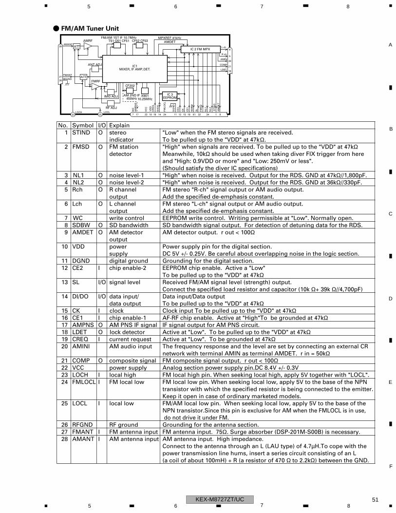
No. Symbol I/O Explain1 STIND O stereo "Low" when the FM stereo signals are received.
indicator To be pulled up to the "VDD" at 47kΩ.2 FMSD FM station "High" when signals are received. To be pulled up to the "VDD" at 47kΩ
detector Meanwhile, 10kΩ should be used when taking diver FIX trigger from hereand "High: 0.9VDD or more" and "Low: 250mV or less".(Should satisfy the diver IC specifications)
3 NL1 O noise level-1 "High" when noise is received. Output for the RDS. GND at 47kΩ//1,800pF.4 NL2 O noise level-2 "High" when noise is received. Output for the RDS. GND at 36kΩ//330pF.5 Rch O R channel FM stereo "R-ch" signal output or AM audio output.
output Add the specified de-emphasis constant. 6 Lch O L channel FM stereo "L-ch" signal output or AM audio output.
output Add the specified de-emphasis constant. 7 WC write control EEPROM write control. Writing permissible at "Low". Normally open.8 SDBW O SD bandwidth SD bandwidth signal output. For detection of detuning data for the RDS.9 AMDET O AM detector AM detector output. r out < 100Ω
output10 VDD power Power supply pin for the digital section.
supply DC 5V +/- 0.25V. Be careful about overlapping noise in the logic section.11 DGND digital ground Grounding for the digital section.12 CE2 I chip enable-2 EEPROM chip enable. Active a "Low"
To be pulled up to the "VDD" at 47kΩ13 SL I/O signal level Received FM/AM signal level (strength) output.
Connect the specified load resistor and capacitor (10k Ω+ 39k Ω//4,700pF)14 DI/DO I/O data input/ Data input/Data output
data output To be pulled up to the "VDD" at 47kΩ15 CK I clock Clock input To be pulled up to the "VDD" at 47kΩ16 CE1 I chip enable-1 AF·RF chip enable. Active at "High"To be grounded at 47kΩ17 AMPNS AM PNS IF signal IF signal output for AM PNS circuit.18 LDET O lock detector Active at "Low". To be pulled up to the "VDD" at 47kΩ19 CREQ I current request Active at "Low". To be grounded at 47kΩ20 AMINI AM audio input The frequency response and the level are set by connecting an external CR
network with terminal AMIN as terminal AMDET. r in = 50kΩ21 COMP O composite signal FM composite signal output. r out < 100Ω22 VCC power supply Analog section power supply pin.DC 8.4V +/- 0.3V 23 LOCH I local high FM local high pin. When seeking local high, apply 5V together with "LOCL". 24 FMLOCL I FM local low FM local low pin. When seeking local low, apply 5V to the base of the NPN
transistor with which the specified resistor is being connected to the emitter. Keep it open in case of ordinary marketed models.
25 LOCL I local low FM/AM local low pin. When seeking local low, apply 5V to the base of the NPN transistor.Since this pin is exclusive for AM when the FMLOCL is in use,do not drive it under FM.
26 RFGND RF ground Grounding for the antenna section.27 FMANT I FM antenna input FM antenna input. 75Ω. Surge absorber (DSP-201M-S00B) is necessary.28 AMANT I AM antenna input AM antenna input. High impedance.
Connect to the antenna through an L (LAU type) of 4.7µH.To cope with thepower transmission line hums, insert a series circuit consisting of an L(a coil of about 100mH) + R (a resistor of 470 Ω to 2.2kΩ) between the GND.
IC 3EEPROM
28
27
FM/AM 1ST IF 10.7MHzT51 Q51 CF51 CF52 CF53
IC1MIXER, IF AMP, DET.
6
21
18LDET
COMP
2225 10 14 12 15 16 81 32 34
CF202
VD
D
VC
C
DI/D
O
CE
2
CK
CE
1
SD
BW
SL
FMS
D
NL1
NL2
IC 2 FM MPX
AMANT
FMANT
ATT
ATT
AMRF
FMRF
IMG ADJ
RF ADJ
X90110.25MHz
ANT ADJ
LOCL23
LOCH
AMDETMPXREF 41kHz
AM 2ND IF450kHz
19
CR
EQ
11
DG
ND
1
ST
IND
L ch
5R ch
924
AM
DE
T
FMLO
CL
20
177
AM
PN
SW
C
26 RFGND
AMIN
- FM/AM Tuner Unit
O
O
515 6 7 8
1 2 3 4
C
D
F
A
B
E
KEX-M8727ZT/UC52
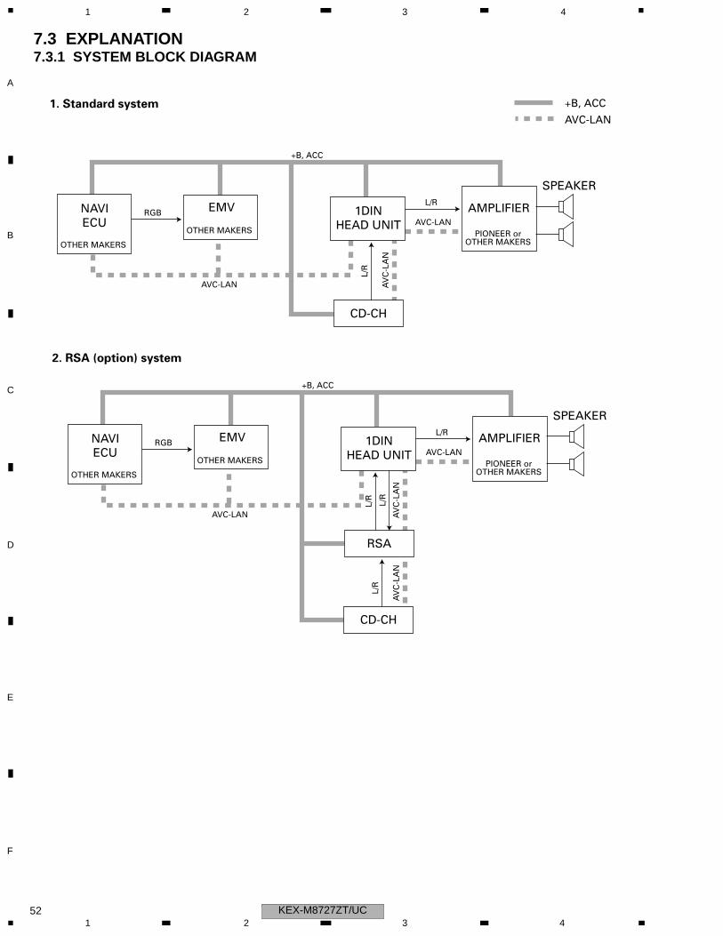
7.3 EXPLANATION7.3.1 SYSTEM BLOCK DIAGRAM
L/R
AV
C-L
AN
RGBL/R AMPLIFIER
PIONEER orOTHER MAKERS
SPEAKER
1. Standard system
1DINHEAD UNIT AVC-LAN
+B, ACC
+B, ACC
AVC-LAN
CD-CH
EMV
OTHER MAKERS
NAVIECU
OTHER MAKERS
AVC-LAN
2. RSA (option) systemL/
R
AV
C-L
AN
RGBL/R AMPLIFIER
PIONEER orOTHER MAKERS
SPEAKER
1DINHEAD UNIT AVC-LAN
+B, ACC
RSA
EMV
OTHER MAKERS
NAVIECU
OTHER MAKERS
AVC-LAN
CD-CH
L/R
AV
C-L
AN
L/R
1 2 3 4
5 6 7 8
C
D
F
A
B
E
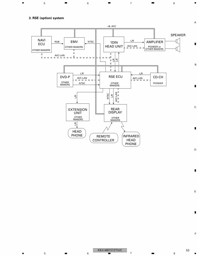
KEX-M8727ZT/UC
RGB
L/R
NTSC
REARDISPLAY
AMPLIFIERPIONEER or
OTHER MAKERS
SPEAKER
DVD-P
OTHERMAKERS
RSE ECU
OTHERMAKERS
1DINHEAD UNIT
HEADPHONE
OTHERMAKERS
3. RSE (option) system
EXTENSIONUNITOTHER
MAKERS
INFRAREDHEAD
PHONE
REMOTECONTROLLER
L/R
L/RL/R
AVC-LAN
AVC-LAN AVC-LAN
+B, ACC
CD-CH
PIONEER
OTHER MAKERS
EMVNAVIECU
OTHER MAKERS
AVC-LAN
AV
C-L
AN
L/R
NT
SC
L/R
L/R
NTSC
L/R
535 6 7 8
1 2 3 4
C
D
F
A
B
E
KEX-M8727ZT/UC54
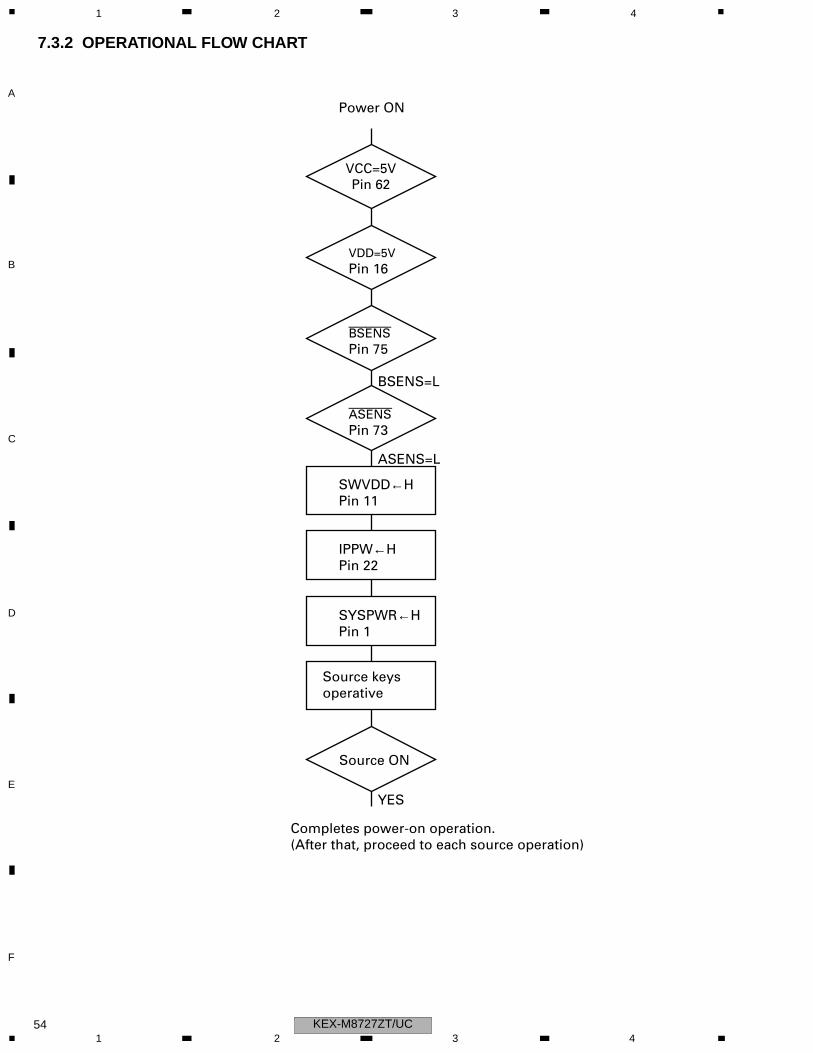
7.3.2 OPERATIONAL FLOW CHART
VCC=5VPin 62
Power ON
BSENS=L
ASENS=L
YES
VDD=5VPin 16
bsensPin 75
asensPin 73
SYSPWR←HPin 1
IPPW←HPin 22
SWVDD←HPin 11
Source keys operative
Completes power-on operation.(After that, proceed to each source operation)
Source ON
1 2 3 4
5 6 7 8
C
D
F
A
B
E
KEX-M8727ZT/UC
7.4 CLEANING
Before shipping out the product, be sure to clean the following portions by using the prescribed cleaning tools:
Portions to be cleaned Cleaning tools
Cassette headsPinch rollersCapstans
Cleaning paper : GED-008
555 6 7 8

8. OPERATIONS
-RADIO
MANUAL TUNINGPOWER
ON/OFF,
VOLUME
AM
SEEK
UP/DOWN
FM
-CD,DVD
DISC
SELECT
CD,DVD
DIRECTION
CHANGE
TAPE
AUTO
PROGRAM
SEARCH
TRACK
SELECT
EJECT-TAPE
TRAFFIC INFORMATION
- KEX-M8727ZT/UC, KEX-M8527ZT/UC
POWER
ON/OFF,
VOLUME
POWER
ON/OFF,
VOLUME
PIONEER CORPORATION 4-1, Meguro 1-chome, Meguro-ku, Tokyo 153-8654, JapanPIONEER ELECTRONICS (USA) INC. P.O. Box 1760, Long Beach, CA 90801-1760, U.S.A.PIONEER EUROPE NV Haven 1087, Keetberglaan 1, 9120 Melsele, BelgiumPIONEER ELECTRONICS ASIACENTRE PTE. LTD. 253 Alexandra Road, #04-01, Singapore 159936
PIONEER CORPORATION 2002K-ZZS.AUG. 2002 Printed in Japan
Recommended