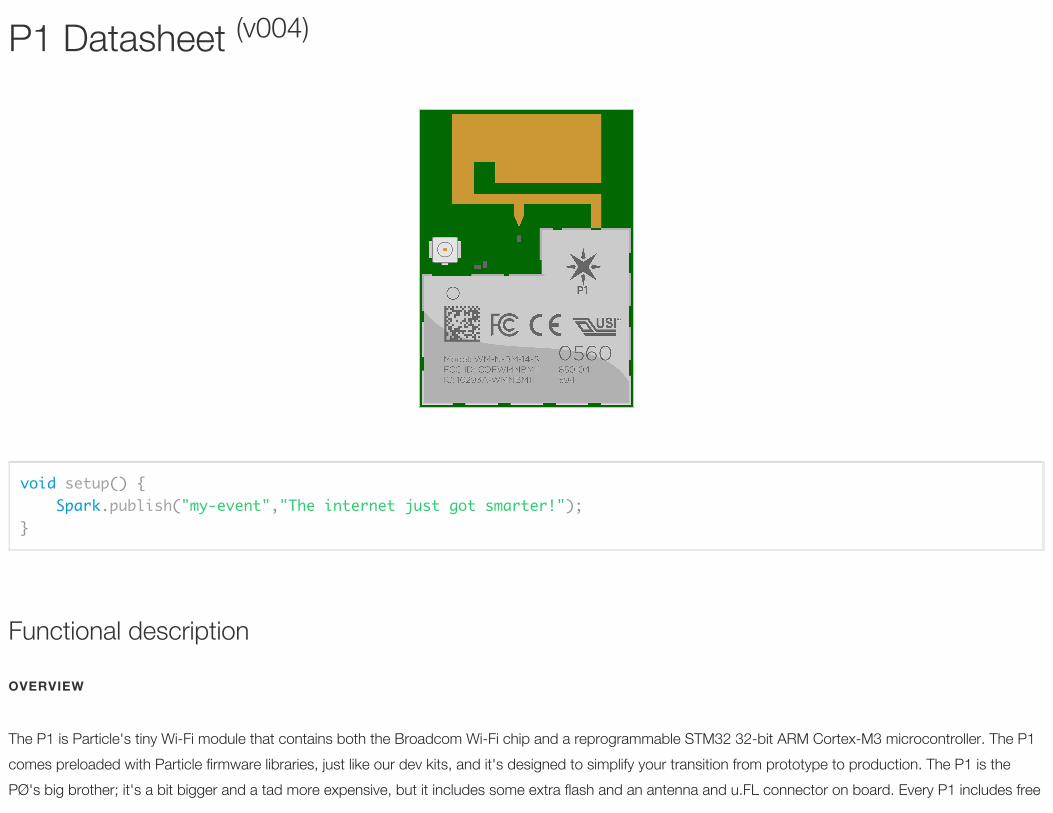
The P1 is Particle's tiny Wi-Fi module that contains both the Broadcom Wi-Fi chip and a reprogrammable STM32 32-bit ARM Cortex-M3 microcontroller. The P1comes preloaded with Particle firmware libraries, just like our dev kits, and it's designed to simplify your transition from prototype to production. The P1 is thePØ's big brother; it's a bit bigger and a tad more expensive, but it includes some extra flash and an antenna and u.FL connector on board. Every P1 includes free
P1 Datasheet (v004)
Functional description
OVERVIEW
void setup() { Spark.publish("my-event","The internet just got smarter!");}
cloud service.
Particle P1 Wi-Fi moduleBroadcom BCM43362 Wi-Fi chip802.11b/g/n Wi-FiSTM32F205 120Mhz ARM Cortex M31MB flash, 128KB RAM1MB external SPI flashIntegrated PCB antennaIntegrated u.FL connector for external antennaIntegrated RF switch
25 Mixed-signal GPIO and advanced peripheralsOpen source designReal-time operating system (FreeRTOS)Soft AP setupFCC, CE and IC certified
FEATURES
Interfaces
BLOCK DIAGRAM
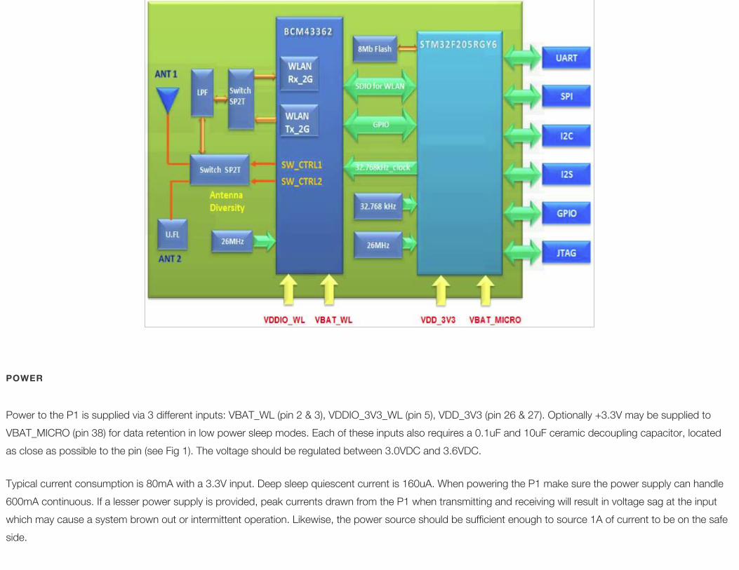
Power to the P1 is supplied via 3 different inputs: VBAT_WL (pin 2 & 3), VDDIO_3V3_WL (pin 5), VDD_3V3 (pin 26 & 27). Optionally +3.3V may be supplied toVBAT_MICRO (pin 38) for data retention in low power sleep modes. Each of these inputs also requires a 0.1uF and 10uF ceramic decoupling capacitor, locatedas close as possible to the pin (see Fig 1). The voltage should be regulated between 3.0VDC and 3.6VDC.
Typical current consumption is 80mA with a 3.3V input. Deep sleep quiescent current is 160uA. When powering the P1 make sure the power supply can handle600mA continuous. If a lesser power supply is provided, peak currents drawn from the P1 when transmitting and receiving will result in voltage sag at the inputwhich may cause a system brown out or intermittent operation. Likewise, the power source should be sufficient enough to source 1A of current to be on the safeside.
POWER
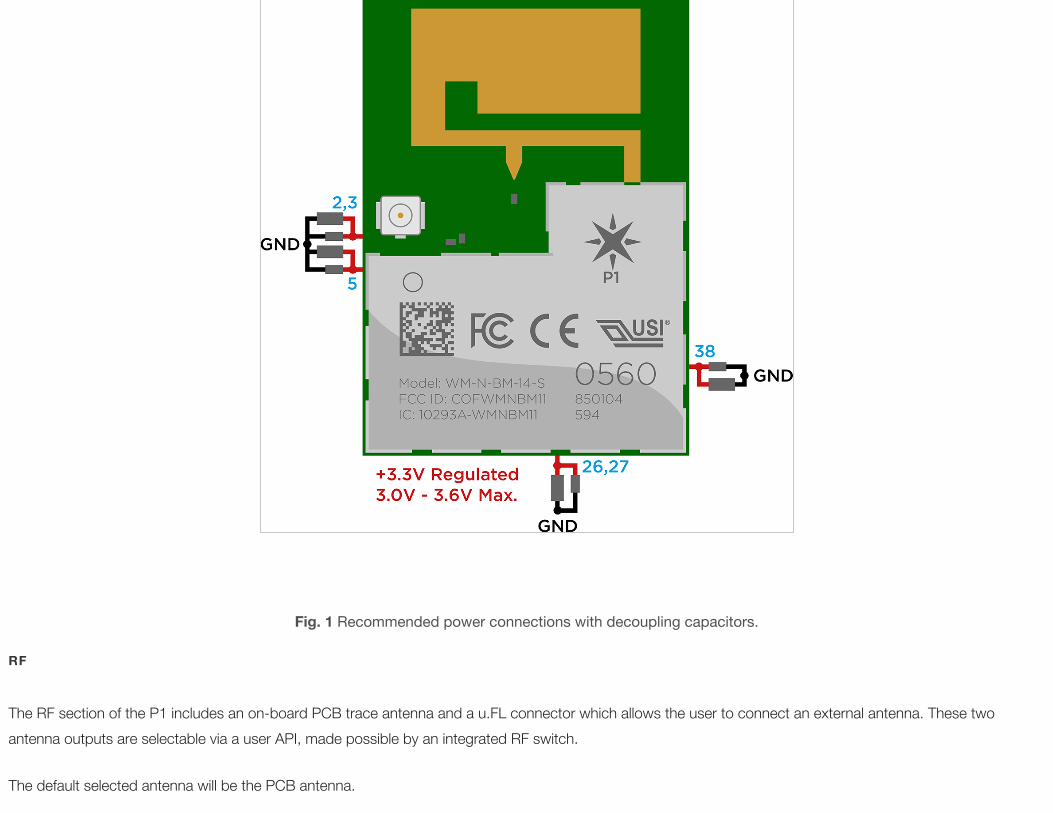
Fig. 1 Recommended power connections with decoupling capacitors.
The RF section of the P1 includes an on-board PCB trace antenna and a u.FL connector which allows the user to connect an external antenna. These twoantenna outputs are selectable via a user API, made possible by an integrated RF switch.
The default selected antenna will be the PCB antenna.
RF
The area surrounding the PCB antenna on the carrier PCB should be free of ground planes and signal traces for maximum Wi-Fi performance.
Antenna Type Manufacturer MFG. Part # Gain
Dipole antenna LumenRadio 104-1001 2.15dBi
PCB Antenna Included - -
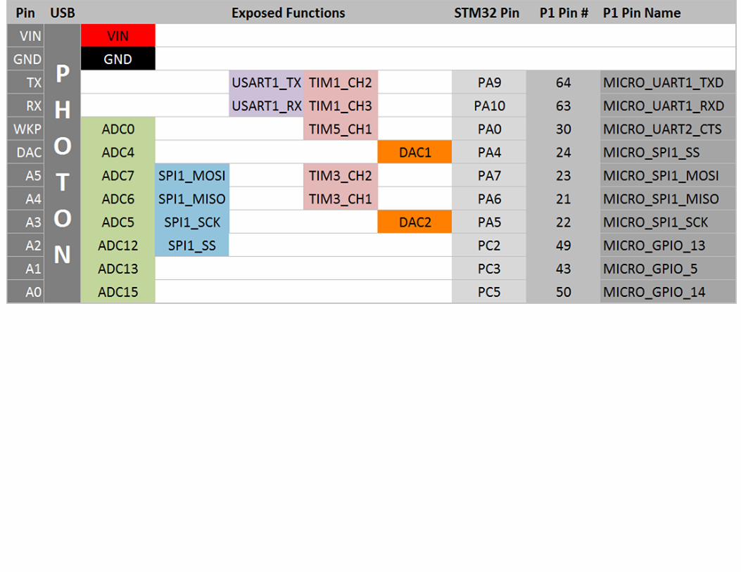
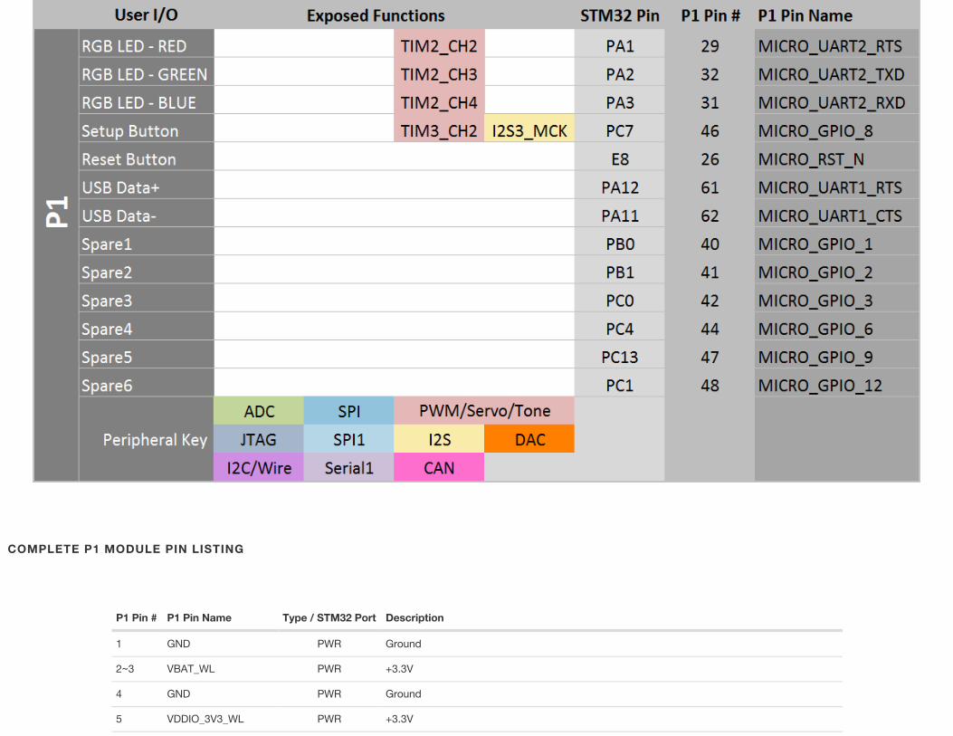
The P1 module has ton of capability in a super small footprint, with analog, digital and communication interfaces.
Note: P1 pin names will be preserved as they are named in the USI datasheet, however for the scope of this datasheet we will also refer to them as their Photonand code equivalents, i.e. D7 instead of MICRO_JTAG_TMS and A2 instead of MICRO_GPIO_13. This will help to simplify descriptions, while providing a quickreference for code that can be written for the P1 such as int value = analogRead(A2);
Peripheral Type Qty Input(I) / Output(O) FT / 3V3
Digital 18 I/O FT/3V3
Analog (ADC) 8 I 3V3
Analog (DAC) 2 O 3V3
SPI 2 I/O 3V3
I2S 1 I/O 3V3
I2C 1 I/O FT
CAN 1 I/O FT
USB 1 I/O 3V3
PWM 9 O 3V3
Spare 6 I/O FT/3V3
FCC APPROVED ANTENNAS
PERIPHERALS AND GPIO
[1] [2]
3
[4]
Notes:
FT = 5.0V tolerant pins. All pins except A3 and DAC are 5V tolerant (when not in analog mode). If used as a 5V input the pull-up/pull-down resistor must bedisabled.
3V3 = 3.3V max pins.
PWM is available on D0, D1, D2, D3, A4, A5, WKP, RX, TX with a caveat: PWM timer peripheral is duplicated on two pins (A5/D2) and (A4/D3) for 7 totalindependent PWM outputs. For example: PWM may be used on A5 while D2 is used as a GPIO, or D2 as a PWM while A5 is used as an analog input. HoweverA5 and D2 cannot be used as independently controlled PWM outputs at the same time.
There are 6 extra pins that have digital I/O capability. There are other peripherals that are available on these pins as well, which will be implemented in firmwareand documented in a future version of this document.
When using the P1 module, it is very important to remember that your device must have an RGB LED to show the user the connectivity status. Also required is aSETUP and RESET button to enter various Device Modes. By default the RGB LED outputs are configured for a Common Anode type of LED. These componentsshould be wired according to the P1 Reference Design - User I/O.
Pin D3 through D7 are JTAG interface pins. These can be used to reprogram your P1 bootloader or user firmware image with standard JTAG tools such as theST-Link v2, J-Link, R-Link, OLIMEX ARM-USB-TINI-H, and also the FTDI-based Particle JTAG Programmer.
Photon Pin Description STM32 Pin P1 Pin # P1 Pin Name Default Internal
D7 JTAG_TMS PA13 54 MICRO_JTAG_TMS ~40k pull-up
D6 JTAG_TCK PA14 55 MICRO_JTAG_TCK ~40k pull-down
D5 JTAG_TDI PA15 53 MICRO_JTAG_TDI ~40k pull-up
D4 JTAG_TDO PB3 52 MICRO_JTAG_TDO Floating
[1]
[2]
[3]
[4]
RGB LED, SETUP AND RESET BUTTON
JTAG
[1]
D3 JTAG_TRST PB4 51 MICRO_JTAG_TRSTN ~40k pull-up
3V3 Power
GND Ground
RST Reset
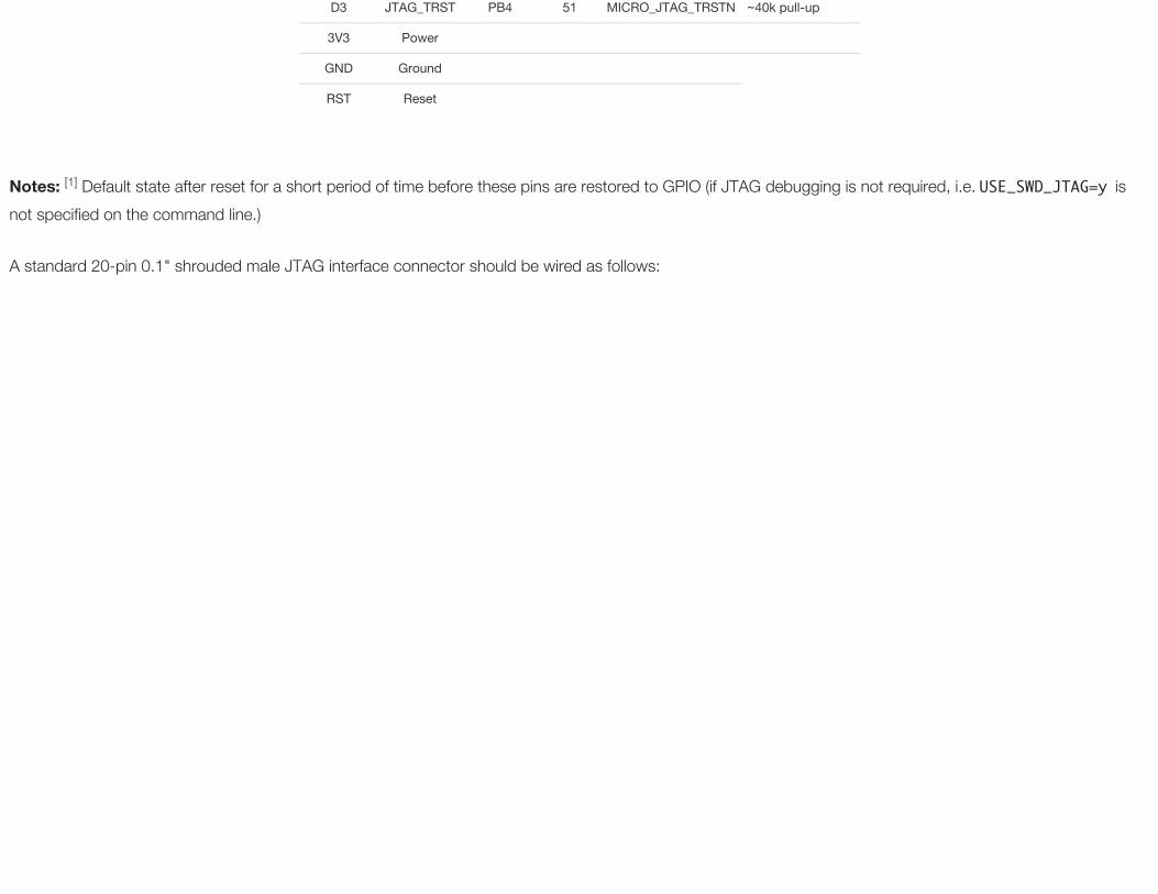
Notes: Default state after reset for a short period of time before these pins are restored to GPIO (if JTAG debugging is not required, i.e.USE_SWD_JTAG=y isnot specified on the command line.)
A standard 20-pin 0.1" shrouded male JTAG interface connector should be wired as follows:
[1]
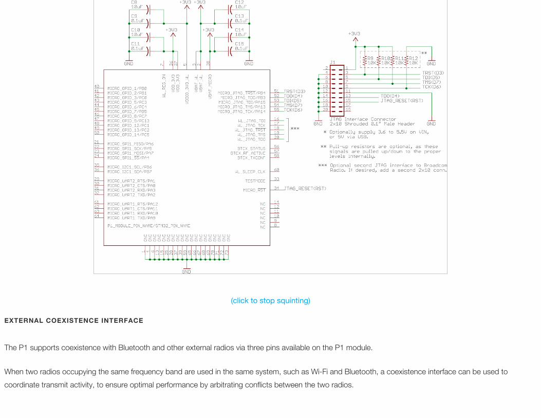
(click to stop squinting)
The P1 supports coexistence with Bluetooth and other external radios via three pins available on the P1 module.
When two radios occupying the same frequency band are used in the same system, such as Wi-Fi and Bluetooth, a coexistence interface can be used tocoordinate transmit activity, to ensure optimal performance by arbitrating conflicts between the two radios.
EXTERNAL COEXISTENCE INTERFACE
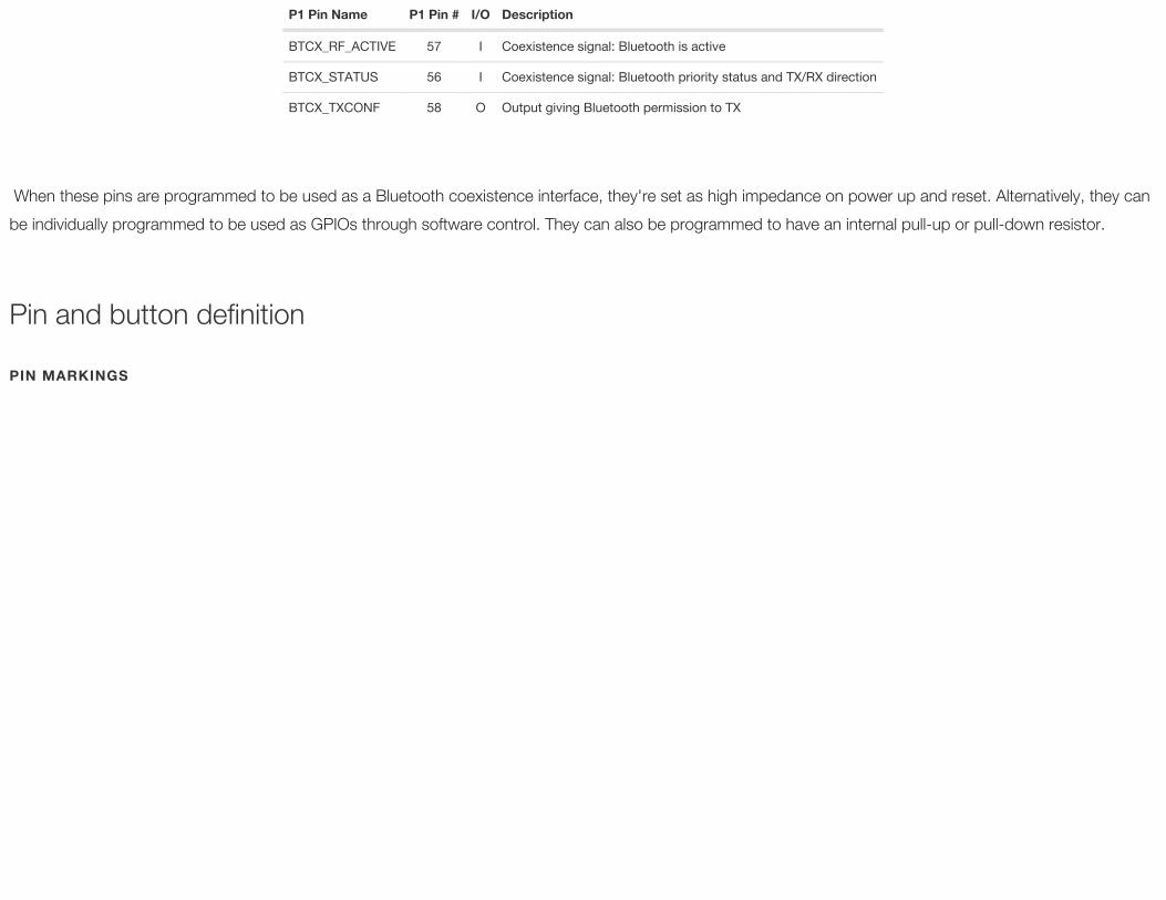
P1 Pin Name P1 Pin # I/O Description
BTCX_RF_ACTIVE 57 I Coexistence signal: Bluetooth is active
BTCX_STATUS 56 I Coexistence signal: Bluetooth priority status and TX/RX direction
BTCX_TXCONF 58 O Output giving Bluetooth permission to TX
When these pins are programmed to be used as a Bluetooth coexistence interface, they're set as high impedance on power up and reset. Alternatively, they canbe individually programmed to be used as GPIOs through software control. They can also be programmed to have an internal pull-up or pull-down resistor.
Pin and button definition
PIN MARKINGS
Pin Description
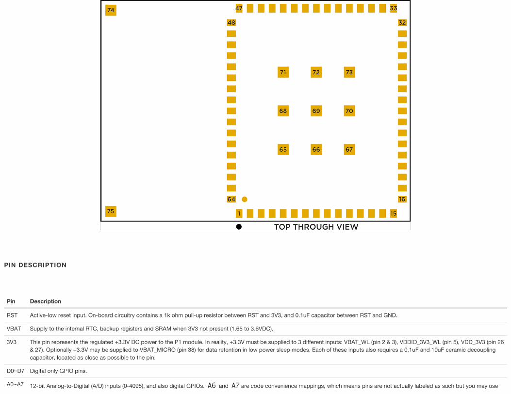
RST Active-low reset input. On-board circuitry contains a 1k ohm pull-up resistor between RST and 3V3, and 0.1uF capacitor between RST and GND.
VBAT Supply to the internal RTC, backup registers and SRAM when 3V3 not present (1.65 to 3.6VDC).
3V3 This pin represents the regulated +3.3V DC power to the P1 module. In reality, +3.3V must be supplied to 3 different inputs: VBAT_WL (pin 2 & 3), VDDIO_3V3_WL (pin 5), VDD_3V3 (pin 26& 27). Optionally +3.3V may be supplied to VBAT_MICRO (pin 38) for data retention in low power sleep modes. Each of these inputs also requires a 0.1uF and 10uF ceramic decouplingcapacitor, located as close as possible to the pin.
D0~D7 Digital only GPIO pins.
A0~A7 12-bit Analog-to-Digital (A/D) inputs (0-4095), and also digital GPIOs. A6 and A7are code convenience mappings, which means pins are not actually labeled as such but you may use
PIN DESCRIPTION
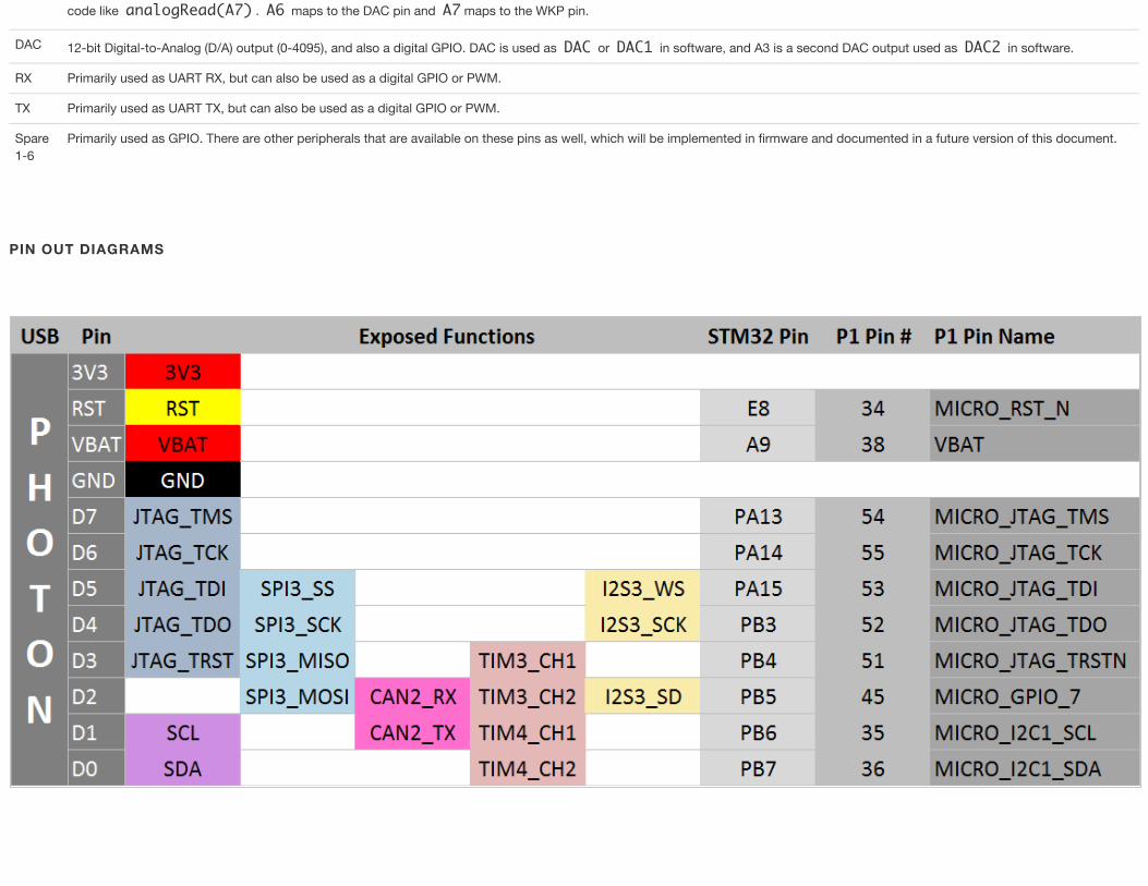
code like analogRead(A7). A6 maps to the DAC pin and A7maps to the WKP pin.
DAC 12-bit Digital-to-Analog (D/A) output (0-4095), and also a digital GPIO. DAC is used as DAC or DAC1 in software, and A3 is a second DAC output used as DAC2 in software.
RX Primarily used as UART RX, but can also be used as a digital GPIO or PWM.
TX Primarily used as UART TX, but can also be used as a digital GPIO or PWM.
Spare1-6
Primarily used as GPIO. There are other peripherals that are available on these pins as well, which will be implemented in firmware and documented in a future version of this document.
PIN OUT DIAGRAMS
P1 Pin # P1 Pin Name Type / STM32 Port Description
1 GND PWR Ground
2~3 VBAT_WL PWR +3.3V
4 GND PWR Ground
5 VDDIO_3V3_WL PWR +3.3V
COMPLETE P1 MODULE PIN LISTING
6 GND PWR Ground
7 WL_REG_ON PWR BCM43362 Debugging Pin
8~12 NC NC NC
13 GND PWR Ground
14 NC NC NC
15 GND PWR Ground
16 WL_JTAG_TDI DEBUG BCM43362 Debugging Pin
17 WL_JTAG_TCK DEBUG BCM43362 Debugging Pin
18 WL_JTAG_TRSTN DEBUG BCM43362 Debugging Pin
19 WL_JTAG_TMS DEBUG BCM43362 Debugging Pin
20 WL_JTAG_TDO DEBUG BCM43362 Debugging Pin
21 MICRO_SPI1_MISO PA6 A4, SPI MISO
22 MICRO_SPI1_SCK PA5 A3, SPI SCK
23 MICRO_SPI1_MOSI PA7 A5, SPI MOSI
24 MICRO_SPI1_SS PA4 DAC, SPI SS
25 GND PWR Ground
26~27 VDD_3V3 PWR +3.3V
28 GND PWR Ground
29 MICRO_UART2_RTS PA1 RGB_LED_RED
30 MICRO_UART2_CTS PA0 WKP
31 MICRO_UART2_RXD PA3 RGB_LED_BLUE
32 MICRO_UART2_TXD PA2 RGB_LED_GREEN
33 TESTMODE PA8 GPIO (see STM32F205 datasheet)
34 MICRO_RST_N I /RESET, Active low MCU reset
35 MICRO_I2C1_SCL PB6 D1, I2C SCL
36 MICRO_I2C1_SDA PB7 D0, I2C SDA
37 GND PWR Ground
38 VBAT_MICRO PWR Supply to the internal RTC, backup registers and SRAM when 3V3 not present (1.65 to 3.6VDC)
39 GND PWR Ground
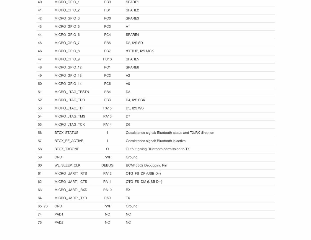
40 MICRO_GPIO_1 PB0 SPARE1
41 MICRO_GPIO_2 PB1 SPARE2
42 MICRO_GPIO_3 PC0 SPARE3
43 MICRO_GPIO_5 PC3 A1
44 MICRO_GPIO_6 PC4 SPARE4
45 MICRO_GPIO_7 PB5 D2, I2S SD
46 MICRO_GPIO_8 PC7 /SETUP, I2S MCK
47 MICRO_GPIO_9 PC13 SPARE5
48 MICRO_GPIO_12 PC1 SPARE6
49 MICRO_GPIO_13 PC2 A2
50 MICRO_GPIO_14 PC5 A0
51 MICRO_JTAG_TRSTN PB4 D3
52 MICRO_JTAG_TDO PB3 D4, I2S SCK
53 MICRO_JTAG_TDI PA15 D5, I2S WS
54 MICRO_JTAG_TMS PA13 D7
55 MICRO_JTAG_TCK PA14 D6
56 BTCX_STATUS I Coexistence signal: Bluetooth status and TX/RX direction
57 BTCX_RF_ACTIVE I Coexistence signal: Bluetooth is active
58 BTCX_TXCONF O Output giving Bluetooth permission to TX
59 GND PWR Ground
60 WL_SLEEP_CLK DEBUG BCM43362 Debugging Pin
61 MICRO_UART1_RTS PA12 OTG_FS_DP (USB D+)
62 MICRO_UART1_CTS PA11 OTG_FS_DM (USB D--)
63 MICRO_UART1_RXD PA10 RX
64 MICRO_UART1_TXD PA9 TX
65~73 GND PWR Ground
74 PAD1 NC NC
75 PAD2 NC NC
Parameter Symbol Min Typ Max Unit
Supply Input Voltage V +3.6 V
Storage Temperature T -40 +85 °C
ESD Susceptibility HBM (Human Body Mode) V 2 kV
Parameter Symbol Min Typ Max Unit
Supply Input Voltage V +3.0 +3.3 +3.6 V
Supply Input Current (VBAT_WL) I 310 mA
Supply Input Current (VDDIO_3V3_WL) I 50 mA
Supply Input Current (VDD_3V3) I 120 mA
Supply Input Voltage V +1.65 +3.6 V
Supply Input Current (VBAT_MICRO) I 19 uA
Operating Current (Wi-Fi on) I 80 100 mA
Operating Current (Wi-Fi on) I 235 430 mA
Operating Current (Wi-Fi on, w/powersave) I 18 100 mA
Operating Current (Wi-Fi off) I 30 40 mA
Sleep Current (5V @ VIN) I 1 2 mA
Deep Sleep Current (5V @ VIN) I 80 100 uA
Operating Temperature T -20 +60 °C
Technical specificationABSOLUTE MAXIMUM RATINGS
3V3-MAX
stg
ESD
RECOMMENDED OPERATING CONDITIONS
3V3[1]
VBAT_WL
VDDIO_3V3_WL
VDD_3V3
VBAT_MICRO
VBAT_MICRO
3V3 avg[1]
3V3 pk[1] [2] [2]
3V3 avg[1] [3]
3V3 avg[1]
Qs
Qds
op
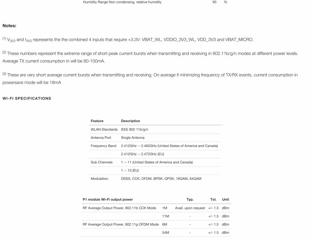
Humidity Range Non condensing, relative humidity 95 %
Notes:
V and I represents the the combined 4 inputs that require +3.3V: VBAT_WL, VDDIO_3V3_WL, VDD_3V3 and VBAT_MICRO.
These numbers represent the extreme range of short peak current bursts when transmitting and receiving in 802.11b/g/n modes at different power levels.Average TX current consumption in will be 80-100mA.
These are very short average current bursts when transmitting and receiving. On average if minimizing frequency of TX/RX events, current consumption inpowersave mode will be 18mA
Feature Description
WLAN Standards IEEE 802 11b/g/n
Antenna Port Single Antenna
Frequency Band 2.412GHz -- 2.462GHz (United States of America and Canada)
2.412GHz -- 2.472GHz (EU)
Sub Channels 1 -- 11 (United States of America and Canada)
1 -- 13 (EU)
Modulation DSSS, CCK, OFDM, BPSK, QPSK, 16QAM, 64QAM
P1 module Wi-Fi output power Typ. Tol. Unit
RF Average Output Power, 802.11b CCK Mode 1M Avail. upon request +/- 1.5 dBm
11M - +/- 1.5 dBm
RF Average Output Power, 802.11g OFDM Mode 6M - +/- 1.5 dBm
54M - +/- 1.5 dBm
[1]3V3 3V3
[2]
[3]
WI-FI SPECIFICATIONS
RF Average Output Power, 802.11n OFDM Mode MCS0 - +/- 1.5 dBm
MCS7 - +/- 1.5 dBm
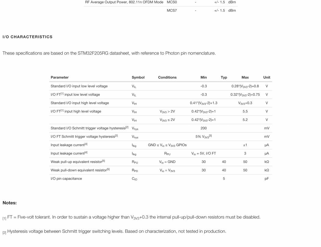
These specifications are based on the STM32F205RG datasheet, with reference to Photon pin nomenclature.
Parameter Symbol Conditions Min Typ Max Unit
Standard I/O input low level voltage V -0.3 0.28*(V -2)+0.8 V
I/O FT input low level voltage V -0.3 0.32*(V -2)+0.75 V
Standard I/O input high level voltage V 0.41*(V -2)+1.3 V +0.3 V
I/O FT input high level voltage V V > 2V 0.42*(V -2)+1 5.5 V
V V ≤ 2V 0.42*(V -2)+1 5.2 V
Standard I/O Schmitt trigger voltage hysteresis V 200 mV
I/O FT Schmitt trigger voltage hysteresis V 5% V mV
Input leakage current I GND ≤ V ≤ V GPIOs ±1 µA
Input leakage current I R V = 5V, I/O FT 3 µA
Weak pull-up equivalent resistor R V = GND 30 40 50 kΩ
Weak pull-down equivalent resistor R V = V 30 40 50 kΩ
I/O pin capacitance C 5 pF
Notes:
FT = Five-volt tolerant. In order to sustain a voltage higher than V +0.3 the internal pull-up/pull-down resistors must be disabled.
Hysteresis voltage between Schmitt trigger switching levels. Based on characterization, not tested in production.
I/O CHARACTERISTICS
IL 3V3
[1]IL 3V3
IH 3V3 3V3
[1]IH 3V3 3V3
IH 3V3 3V3
[2]hys
[2]hys 3V3
[3]
[4]lkg io 3V3
[4]lkg PU io
[5]PU io
[5]PD io 3V3
IO
[1] 3V3
[2]
With a minimum of 100mV.
Leakage could be higher than max. if negative current is injected on adjacent pins.
Pull-up and pull-down resistors are designed with a true resistance in series with switchable PMOS/NMOS. This PMOS/NMOS contribution to the seriesresistance is minimum (~10% order).
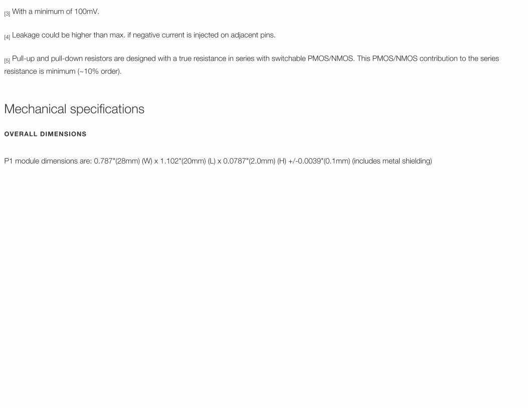
P1 module dimensions are: 0.787"(28mm) (W) x 1.102"(20mm) (L) x 0.0787"(2.0mm) (H) +/-0.0039"(0.1mm) (includes metal shielding)
[3]
[4]
[5]
Mechanical specificationsOVERALL DIMENSIONS
Actual size (so tiny!)
These are the physical dimensions of the P1 module itself, including all pins:
P1 MODULE DIMENSIONS
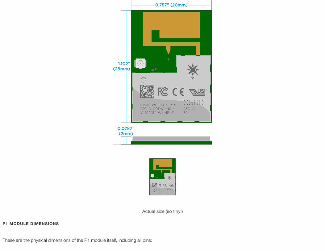
The P1 can be mounted directly on a carrier PCB with following PCB land pattern:
P1 MODULE RECOMMENDED PCB LAND PATTERN
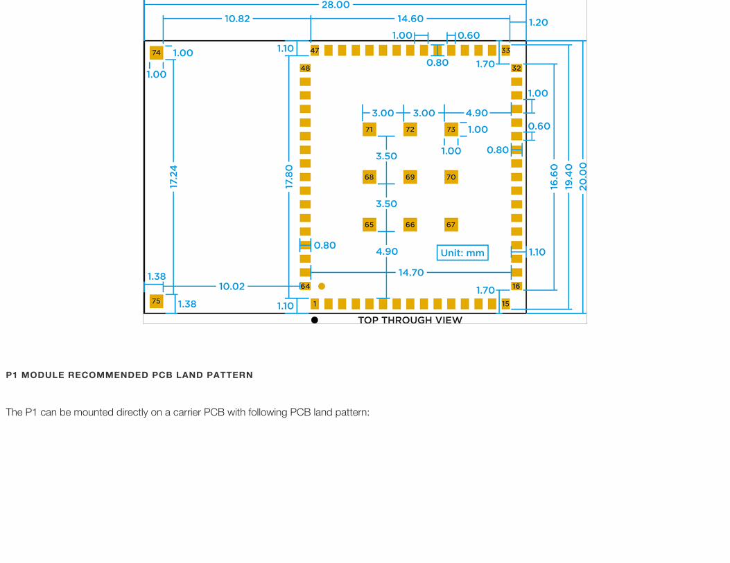
P1 Reference Design SchematicSCHEMATIC - USB
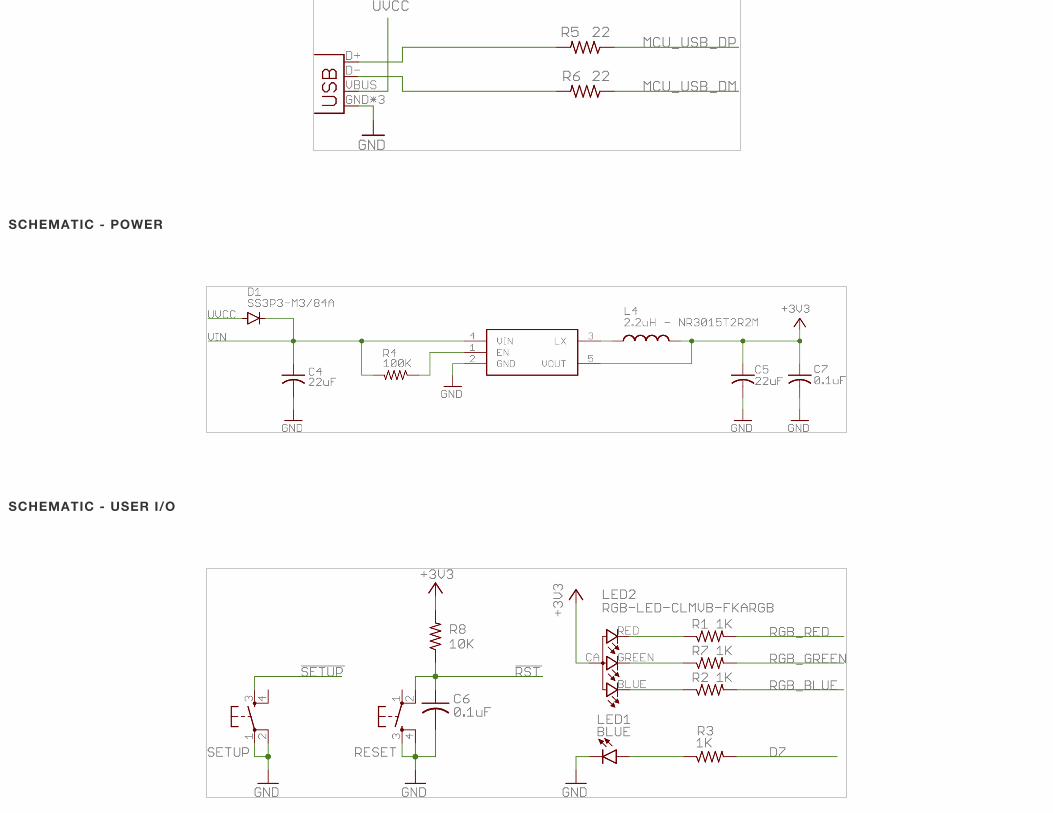
SCHEMATIC - POWER
SCHEMATIC - USER I/O
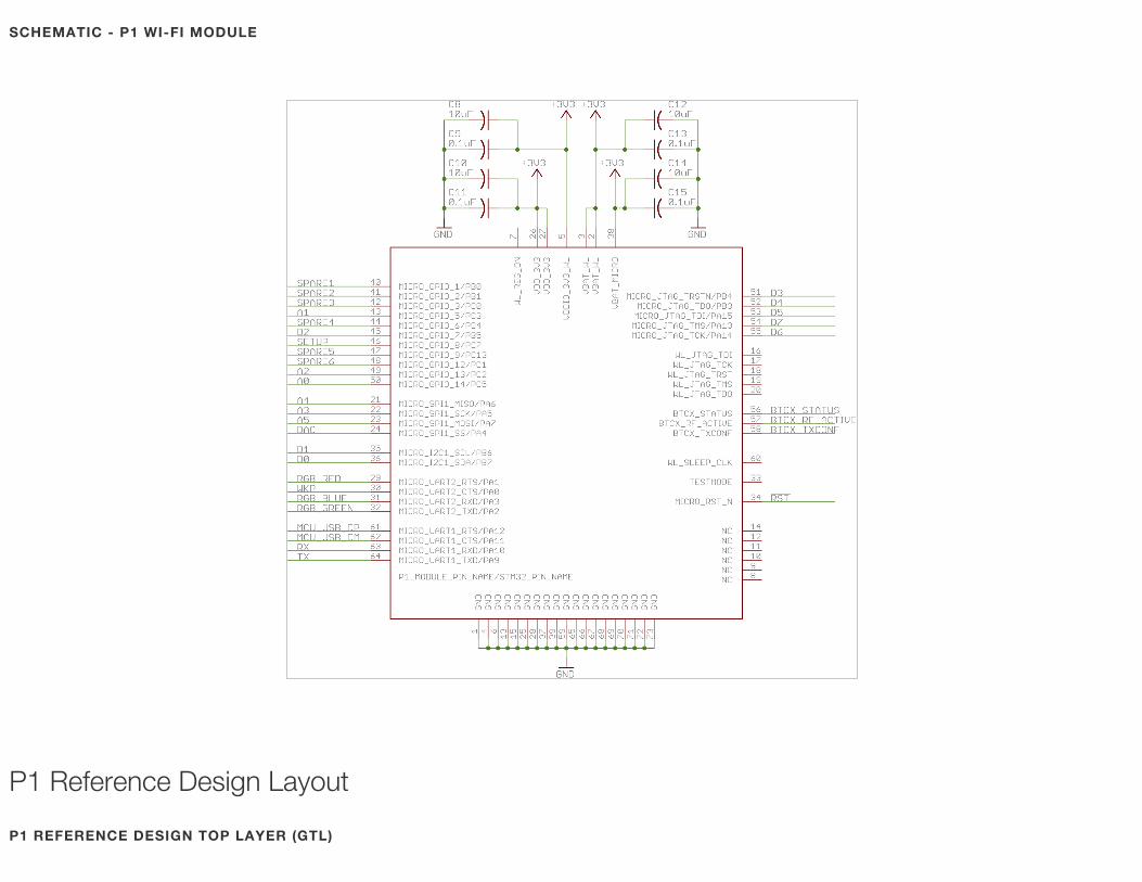
SCHEMATIC - P1 WI-FI MODULE
P1 Reference Design LayoutP1 REFERENCE DESIGN TOP LAYER (GTL)
To be added.
To be added.
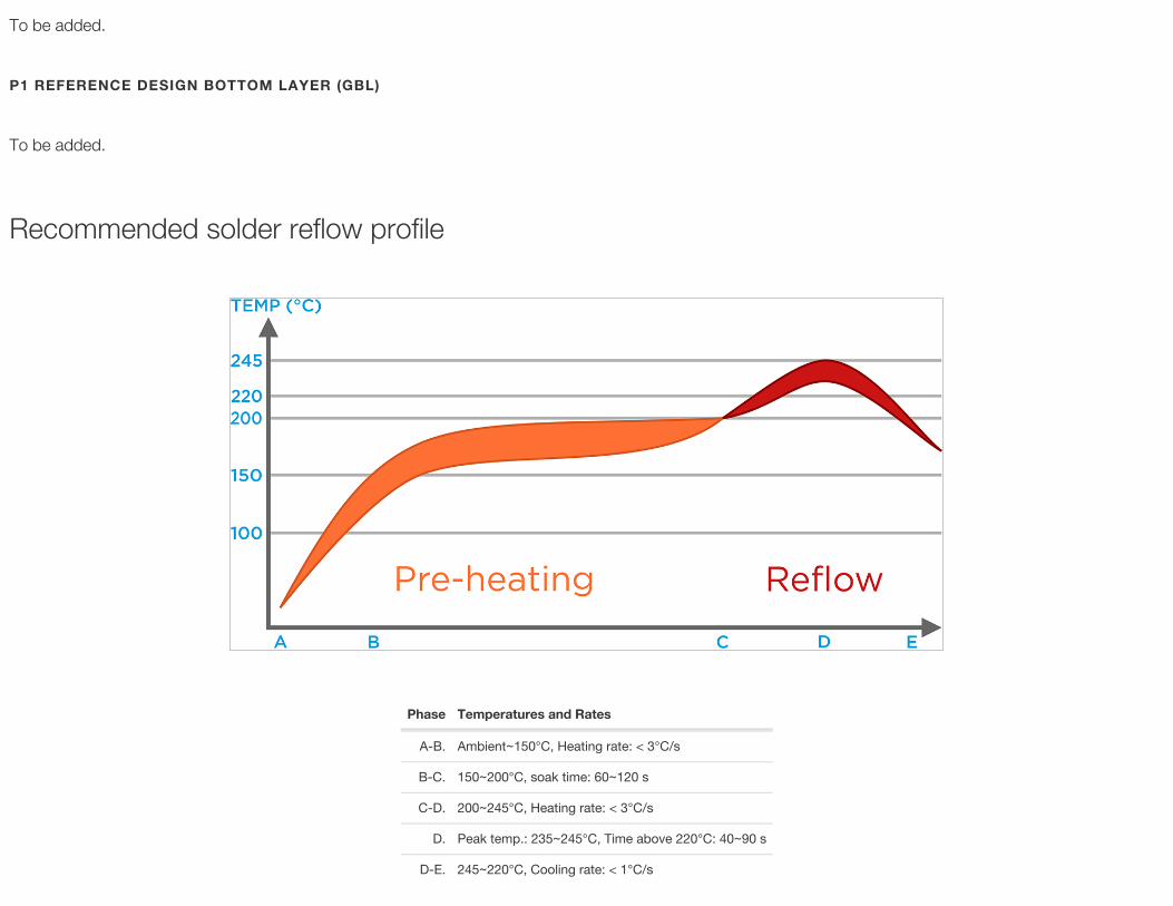
Phase Temperatures and Rates
A-B. Ambient~150°C, Heating rate: < 3°C/s
B-C. 150~200°C, soak time: 60~120 s
C-D. 200~245°C, Heating rate: < 3°C/s
D. Peak temp.: 235~245°C, Time above 220°C: 40~90 s
D-E. 245~220°C, Cooling rate: < 1°C/s
P1 REFERENCE DESIGN BOTTOM LAYER (GBL)
Recommended solder reflow profile
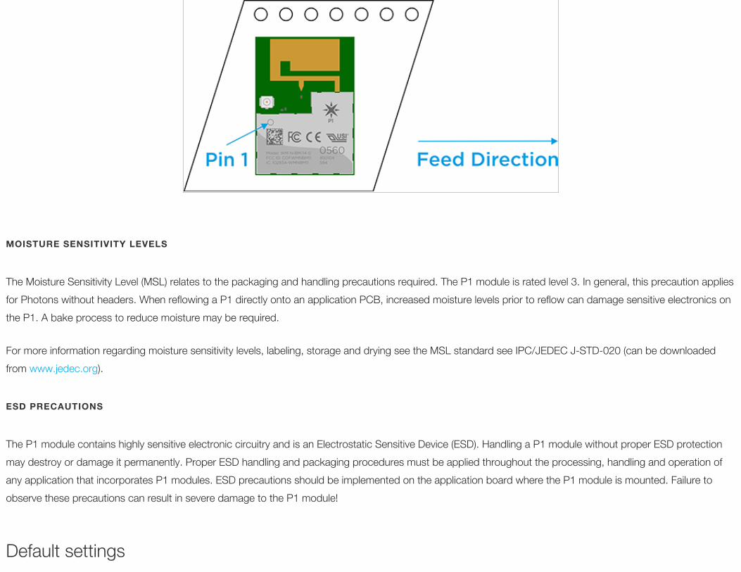
P1 modules are available from store.particle.io as cut tape in quantities of 10 each.
RoHSCEFCC ID: COFWMNBM11IC: 10293A-WMNBM11
Ordering information
Qualification and approvals
Product handlingTAPE AND REEL INFO
The Moisture Sensitivity Level (MSL) relates to the packaging and handling precautions required. The P1 module is rated level 3. In general, this precaution appliesfor Photons without headers. When reflowing a P1 directly onto an application PCB, increased moisture levels prior to reflow can damage sensitive electronics onthe P1. A bake process to reduce moisture may be required.
For more information regarding moisture sensitivity levels, labeling, storage and drying see the MSL standard see IPC/JEDEC J-STD-020 (can be downloadedfrom www.jedec.org).
The P1 module contains highly sensitive electronic circuitry and is an Electrostatic Sensitive Device (ESD). Handling a P1 module without proper ESD protectionmay destroy or damage it permanently. Proper ESD handling and packaging procedures must be applied throughout the processing, handling and operation ofany application that incorporates P1 modules. ESD precautions should be implemented on the application board where the P1 module is mounted. Failure toobserve these precautions can result in severe damage to the P1 module!
MOISTURE SENSITIVITY LEVELS
ESD PRECAUTIONS
Default settings
The P1 module comes preprogrammed with a bootloader and a user application called Tinker. This application works with an iOS and Android app also namedTinker that allows you to very easily toggle digital pins, take analog and digital readings and drive variable PWM outputs.
The bootloader allows you to easily update the user application via several different methods, USB, OTA, Serial Y-Modem, and also internally via the FactoryReset procedure. All of these methods have multiple tools associated with them as well.
You may use the online Web IDE Particle Build to code, compile and flash a user application OTA (Over The Air). Particle Dev is a local tool that uses the Cloud tocompile and flash OTA as well. There is also a package Spark DFU-UTIL for Particle Dev that allows for Cloud compiling and local flashing via DFU over USB.This requires dfu-util to be installed on your system. 'dfu-util' can also be used with Particle CLI for Cloud compiling and local flashing via the command line.Finally the lowest level of development is available via the GNU GCC toolchain for ARM, which offers local compile and flash via dfu-util. This gives the usercomplete control of all source code and flashing methods. This is an extensive list, however not exhaustive.
Radio Frequency
SMT
Surface Mount Technology (often associated with SMD which is a surface mount device).
AP
Access Point
USB
Universal Serial Bus
Quiescent current
Current consumed in the deepest sleep state
FT
Five-tolerant; Refers to a pin being tolerant to 5V.
3V3
+3.3V; The regulated +3.3V supply rail. Also used to note a pin is only 3.3V tolerant.
RTC
Glossary
Real Time Clock
OTA
Over The Air; describing how firmware is transferred to the device.
Federal Communication Commission Interference Statement This equipment has been tested and found to comply with the limits for a Class B digitaldevice, pursuant to Part 15 of the FCC Rules. These limits are designed to provide reasonable protection against harmful interference in a residential installation.This equipment generates, uses and can radiate radio frequency energy and, if not installed and used in accordance with the instructions, may cause harmfulinterference to radio communications. However, there is no guarantee that interference will not occur in a particular installation. If this equipment does causeharmful interference to radio or television reception, which can be determined by turning the equipment off and on, the user is encouraged to try to correct theinterference by one of the following measures:
Reorient or relocate the receiving antenna.Increase the separation between the equipment and receiver.Connect the equipment into an outlet on a circuit different from that to which the receiver is connected.Consult the dealer or an experienced radio/TV technician for help.
FCC Caution: Any changes or modifications not expressly approved by the party responsible for compliance could void the user's authority to operate thisequipment. This device complies with Part 15 of the FCC Rules. Operation is subject to the following two conditions:
1. This device may not cause harmful interference, and2. This device must accept any interference received, including interference that may cause undesired operation.
FCC Radiation Exposure Statement: This equipment complies with FCC radiation exposure limits set forth for an uncontrolled environment. This transmittermodule must not be co-located or operating in conjunction with any other antenna or transmitter. This End equipment should be installed and operated with aminimum distance of 20 centimeters between the radiator and your body.
IMPORTANT NOTE: In the event that these conditions can not be met (for example certain laptop configurations or co-location with another transmitter), thenthe FCC authorization is no longer considered valid and the FCC ID can not be used on the final product. In these circumstances, the OEM integrator will beresponsible for re-evaluating the end product (including the transmitter) and obtaining a separate FCC authorization.
FCC IC CE Warnings and End Product Labeling Requirements
End Product Labeling The final end product must be labeled in a visible area with the following:
Contains FCC ID: 2AEMI-PHOTON
Manual Information to the End User The OEM integrator has to be aware not to provide information to the end user regarding how to install or remove this RFmodule in the user’s manual of the end product which integrates this module.
Canada Statement This device complies with Industry Canada’s licence-exempt RSSs. Operation is subject to the following two conditions:
1. This device may not cause interference; and2. This device must accept any interference, including interference that may cause undesired operation of the device.
Le présent appareil est conforme aux CNR d’Industrie Canada applicables aux appareils radio exempts de licence.
L’exploitation est autorisée aux deux conditions suivantes:
1. l’appareil ne doit pas produire de brouillage;2. l’utilisateur de l’appareil doit accepter tout brouillage radioélectrique subi, même si le brouillage est susceptible d’en compromettre le fonctionnement.
Caution Exposure: This device meets the exemption from the routine evaluation limits in section 2.5 of RSS102 and users can obtain Canadian information onRF exposure and compliance. Le dispositif répond à l'exemption des limites d'évaluation de routine dans la section 2.5 de RSS102 et les utilisateurs peuventobtenir des renseignements canadiens sur l'exposition aux RF et le respect.
The final end product must be labelled in a visible area with the following:The Industry Canada certification label of a module shall be clearly visible at alltimes when installed in the host device, otherwise the host device must be labelled to display the Industry Canada certification number of the module, precededby the words “Contains transmitter module”, or the word “Contains”, or similar wording expressing the same meaning, as follows:
Contains transmitter module IC: 20127-PHOTON
This End equipment should be installed and operated with a minimum distance of 20 centimeters between the radiator and your body. Cet équipement devraitêtre installé et actionné avec une distance minimum de 20 centimètres entre le radiateur et votre corps.
The end user manual shall include all required regulatory information/warning as shown in this manual.
Revision Date Author Comments
v001 4-May-2015
BW Initial release
v002 31-May-2015
BW Update assets
v003 1-June-2015
BW Updated VBAT_MICRO info
v004 24-July-2015
BW Added FCC IC CE Warnings and End Product Labeling Requirements, Updated power output, added approved antennas, Corrected DAC2 as A3, Corrected A0 aspin 50, Corrected External Coexistence Interface pin numbers, Added RGB LED, SETUP and RESET button section.
Web
https://www.particle.io
Community Forums
https://community.particle.io
Revision history
Contact
Recommended