1
Treinamento:Testes Paramétricos em
Semicondutores
Setembro 2012
Cyro HemsiEngenheiro de Aplicação
Section 4 – Capacitance Measurement Basics

2
Agenda
• Technology Area Where Capacitance Measurement is Used
• Fundamental of Capacitance Measurement
• Basic Techniques to Achieve Accurate Capacitance Measurement

3
Technology Area Where Capacitance Measurement is Used

4
What is Capacitance ?
Capacitance is amount of charge stored between the electrodes when applying a unit voltage.
L: LengthW: Width
d: Distance
V
Electrode
Dielectrics
Positive charge
Negative charge
Basic Equations
A e: Relative permittivityA: Area of electrode
e0: Permittivity of vacuum
d
W
d
AC 00 L
CVQ
Q: Total charge V: Applied voltage
Relation of Charge and Applied Voltage
Most important equation to remember!!

5
Physical Dimensions of Semiconductor Devices
• Each capacitance represents actual physical dimensions and it is really important information to adjust conditions of manufacturing processes like lithography, etching, deposition time etc.
• Also, those parasitic capacitances are important to determine the gate delay of electric circuit in the logic devices.
Gate Dielectrics
Source Drain
Gate
SemiconductorSubstrate
L
W
dCgb
Cgs
Cgd
Gate-Source Overwrap
Gate-Source Overwrap
MOS FET Inter Connection
Cgb: Gate to body capacitanceCgd: Gate to drain capacitanceCgs: Gate to source capacitance
Inter layer dielectrics
d
Thickness of interlayer dielectrics can be determined from the capacitance between interconnecting wires.
Thickness of dielectrics can be determined from the gate capacitance.
Overwrap width between the gate electrode and drain or source area can be determined from the gate to drain or gate to source capacitances.
Why Are MOSFET Capacitance Measurements Important?
Capacitance versus voltage measurement
+Physical device parameters (area, work function, etc.)
Mathematical Calculations
•Gate oxide capacitance•Gate oxide thickness•Substrate impurity
concentration•Fermi potential•Flat band capacitance•Flat band voltage•Surface charge density•Fixed depletion layer
charge•Threshold voltage
Key Device Parameters
Note that the value of the capacitance varies with applied DC voltage
Page 6
SEQ.

7
Doping Profile of Semiconductor Devices
N-MOS Cap
Space Charge (depletion)
Layer
p-Si
Cg
Cd
Gate DielectricsLd
V
CdCgCgCd
minc
CgCmax
V
High Frequency
Low Frequency
Vth
• CV characteristics of MOS-CAP (MOS-FET) is one of most important measurement item because it reveals various parameters related to the manufacturing process and device operation.
Threshold voltage can be extracted from the intersection point of Cmin and extrapolation of CV curve.
Distribution of boundary defect density by comparing CV curve measured by high frequency(>1 kHz) and low frequency (<10 Hz) CV measurement.
Doping profile can be extracted from the Cmax and Cmin.
Ld: Depth of depletion layerq: Charge of electronNa: Density of acceptor
LdεAε
dsi0c qNa
ε2εd
si0L V
Thickness of gate dielectrics can be extracted from Cmax.

8
Space Charge Layer
N-type
P-type
Residual Resistance
+
-
Photo current
Junction Capacitor
Junction Leakage
0.E+00
2.E+13
4.E+13
6.E+13
-5.0 -2.5 0.0 2.5 5.0
Voltage [V]
1/C
p2 [
F-2
]
157
158
159
160
161
162
163
0 200 400 600 800
Vpp [mV]
Cp
[nF
]
Re|Z|
Im|Z
|
Rs Rp
0
Frequency
RpRs
C
AC Level (mVpp)
Schematic of Solar Cell Impedance Spectroscopy
Drive-level Capacitance Profiling (DLCP)Mott-Schottky Plot
Capacitance Measurements for Solar CellEquivalent circuit model is determined by frequency sweep of impedance to optimize extra circuit to convert DC power generated by solar cell to AC Power.
Carrier density distribution over the depletion width is obtained from the slope of 1/Cp2 to Voltage plot (Mott-Schottky plot )
Defect density distribution is obtained from the Cp to AC voltage amplitude of capacitance measurement plot.

9
Mobility Measurement of Organic Semiconductor Materials
Organic Material
Cgeo: Geographical capacitance
T. Okachi et al. / Thin Solid Films 517 (2008) 1331–1334
tt: Carrier transit timem: Mobility of carrier
2
3
4
Vdc
dtt
d
Vdc
Mobility of carrier is obtained from the maximum frequency of negative differential susceptance −ΔB=−w{C1(w)−Cgeo}.w: angular velocity of measurement signal.
Improvement of mobility of organic material is most critical to put it to practical use.

10
Characterization of Electrostatic Capacitive MEMS (Micro Electro Mechanical System) Sensor
• Mechanical characteristics of MEMS sensor can be obtained from its capacitance to voltage characteristics.
• Electrical capacitance measurement is easier and faster than the measurement by a mechanical stimulus.
• Also frequency dependency of capacitance reveals mechanical response of the diaphragm spring.
Fixed Electrode
Diaphragm Spring
Electrostatic capacitive MEMS sensor detects displacement of diaphragm by mechanical stimulations like acceleration, pressure or sonic wave as a modulation of electrostatic capacitance.
Also, displacement of diaphragm is caused by the applied external bias voltage.
Electrical Field by Applied Bias Bias Voltage or
Displacement
Capacitance
C0
0
Mechanical Stimulus

11
Importance of On-Wafer Capacitance Measurement
• Advantage of On-wafer Measurement– Quick evaluation and lower cost are possible because packaging is not necessary.
• Challenges– There are many possible course of error from the cablings, wafer chuck, probing etc.
Semi-auto prober
Wafer Chuck
Probe
Wafer
To carry out accurate capacitance measurement, specific attention is necessary.
On-wafer measurement becomes standard to develop various devices.

12
Fundamental of Capacitance Measurement

13
Basic Equations Related to Capacitance Measurement
CVQ
dtdV
CIdtdQ
CdVdQ
AtV
jωtjωCexpI
exp(jωt)V
AI
dtdV
IC
IV
Z
f2πω
0tΔV
0t0V
ΔVΔQ
C
Step Voltage
Ramp Voltage
AC Voltage
Z ω1
CIm
Equation to Measure Capacitance
StimulusDerivationBasic
Equation
Most widely-used method by capacitance meter
Capacitance is calculated from the measured charge and amplitude of applied step voltage.
Capacitance is calculated from the measured current and ramp rate of applied ramp voltage.
Capacitance is calculated from the measured impedance and frequency of applied AC signal.

14
Function of Each Terminal of Capacitance Meter
Agilent 4284A
Advantages of Auto Balancing Bridge Method• High accuracy (0.05 % basic accuracy)• Wide frequency range (20 Hz to 100 MHz)• Various choices are available based on frequency range and functions. Agilent 4284A, 4285A, E4980A, E4981A, 4294A, B1500A
LCUR LPOT HPOT HCUR
AV
LCURLPOTHPOTHCUR
0 VV
I
I
I
VZ
Auto Balancing Bridge
Connect terminals based on its functionalities is important to measure capacitance correctly.
Keep “0V” in AC manner by active feedback.So called “Virtual Ground”, not actual ground.
voltage of the test signal applied to DUT
current that flows through DUT
DUT

15
Equivalent Circuit Model and Equations to Extract Capacitance
Cp-RpCp-GCp-D Cp-Q
Series Model
Cs-RsCs-DCs-Q
Cp Rp
Cs
Rs
Cs1
Rs
Re
Rp
1
Admittance Plane
Cp
Im
Re
Appropriate Parameter
Complex Vector Equations
Parallel Model Appropriate Parameter
Complex Vector Equations
Impedance Plane
G: ConductanceD: Dissipation factorQ: Quality factor
CpjRpV
I
ZY
11
Y
CpIm
YRpRe
1 RpG /1
CpRpY
YD
1
Im
Re DQ /1
Im
CsjRs
I
VZ
1
)Im(
1
ZCs
)Re(ZRs
Cs
Rs
Z
ZD
)Im(
)Re(
Choosing appropriate measurement parameter is essential to extract capacitance correctly.
Z
Y

How Do Capacitance Meters Work?
Virtual groundVirtual ground
Z =
=
V2 = I2 x R2
I2
V1
V2
V1R2
V2Hc R2
Hp Lp
Lc
Rs
DUT
V1
I2
I1 = I2
I1
Auto-Balancing Bridge Method
Page 16
virtual ground of the Op Amp
Impedance is calculated by Z = V1*R2/V2.

Four Terminal Pair (4TP) Measurement Method
Hc
Measurement Circuit
Measurement Circuit
Measurement Path
Measurement Path
Connection with DUT
Connection with DUT
V
DUT
Lc Lp Hp
~~
Virtual groundVirtual ground
A
4TP:Minimize residual impedance
Shields:Minimize stray capacitance
Current flow:Minimize inductive coupling
Page 17

B1500A Capacitance Measurement Coverage
5 MHz 110 MHz1 kHz
QSCVB1500A
(MFCMU)4294AB1500A
(SMU)
HFCV Ultra-HFCV
EasyEXPERT 4.x
Thin-gate (<25 A) dielectrics
Standard (>25 A) dielectrics
Page 18

19
Basic Techniques to Achieve Accurate Capacitance Measurement
20
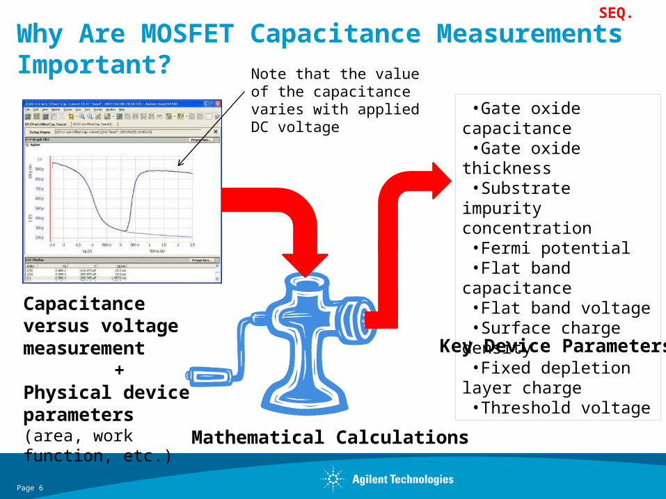
Possible Sources of Measurement Error
• Inappropriate selection of measurement parameter
– Capacitance is extracted based on the equation of the equivalent circuit model for selected measurement parameter.
– Mismatch of equation and equivalent circuit model causes measurement error.
– Selection of appropriate measurement parameter (equivalent circuit ) is important.
• Parasitic capacitance, residual resistance and inductance
– Cablings between the instruments and device affects measurement results.
– Minimizing influence of cablings are critical to achieve accurate measurement.
• Inappropriate execution of compensation
– Compensation is commonly used to remove the influence from the cablings.
– But inappropriate compensation has a devastating impact on measurement results.
– Compensation have to be done in correct manner!!
• Parasitic capacitance of wafer probing system.
– On-wafer measurement has a specific error caused by a parasitic of the wafer chuck not considered when measuring discrete components.
– Special care is required for on-wafer capacitance measurement.

21
Error Caused by Using Inappropriate Selection of Equivalent Circuit Model
Actual Device
Cp Rp
Cs
Rs
Measurement Parameter
Cp-Rp
Cs-Rs
Cp-Rp
Cs-Rs
Measured Value
222
232
1 RsCs
RsCsCsCpm
CsCsm
CpCpm
22
1
CpRpCpCsm
Error caused by
measurement parameter mismatch
Inappropriate selection of measurement parameter increases measurement error.
Quick Tips:If measured capacitance value is stable when measurement frequency is changed, the selection of measurement parameter is appropriate, because error component has frequency dependency.

22
Measurement Parameter Selection for Actual Device
Gate
Sub
Source DrainGate
Cp Rp
Rs
Actual Equivalent Circuit
Gate Resistance
Gate Leakage Junction Resistance
Contact resistance of via
Conditions Parameter to select
RpRs
CpRs
1
ANDCp Rp
Cp-Rp Cp-GCp-D Cp-Q
RsRp
AND
CpRp
1
Cs
Rs
Cs-Rs Cs-DCs-Q
Relatively thick dielectrics of technology node over 90 nm will satisfy either of above.
For more shrunk process, parameter extraction using multi-frequency is necessary.
MOS-FET

23
Error Caused by Cablings
CdevCpar
RresLresTotal impedance measured by LCR Meter
LCR Meter
Output terminals of LCR Meter
Calibration Plane
Device to
Measure
Residual Inductance
Residual Resistance
Parasitic Capacitance
)(
1
CdevCparjLresjRresZm
Additional Error Not related to the measurement frequency
Influence of residual inductance Increases along with a square of frequency
Rres is Included in the Rs when using Cs-Rs mode. But in Cs-Rp mode, Rres is included in the error of measured capacitance.
Higher frequency results in larger measurement error

24
HCUR
HPOT
LPOT
LCUR
Minimizing Error from Cablings
LCUR LPOT HPOT HCUR
LCR Meter
Test Leads for LCR Meter
Output Terminals A
V
LCR Meter
Extends output to the device to measure near as possible by using the test leads of LCR meter
Eliminate parasitic capacitance of cable extension by using coaxial cable and connect shield to the shield of the test leads.
Make unshielded part as short as possible to minimize residual inductance and
Connect shield of test leads each other to terminate four terminal pair.
Test Leads
Connect shield of cable extensions at end of cable each other to minimize residual inductance.
ProbeCable Extension
Measurement Current
Current return to HCUR

END Of section 4
Recommended


![Ch11 [Non-Parametric Tests]](https://img.pdfslide.net/doc/110x75/577cd3291a28ab9e7896d6ef/ch11-non-parametric-tests.jpg)