www.proton-electrotex.com
Power semiconduc to r dev ices
P r o d u c tc a t a l o g

3
Power semiconductor devices
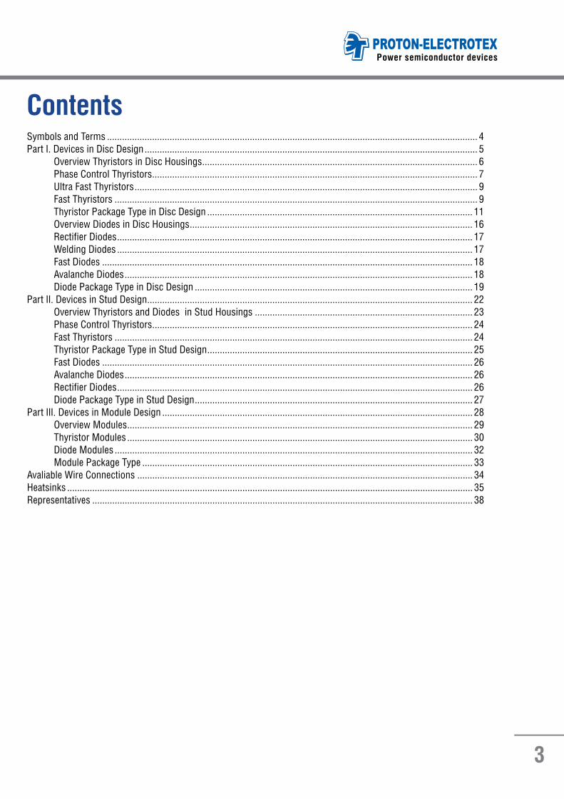
ContentsSymbols and Terms .................................................................................................................................................... 4Part I. Devices in Disc Design ..................................................................................................................................... 5
Overview Thyristors in Disc Housings .............................................................................................................. 6Phase Control Thyristors .................................................................................................................................. 7Ultra Fast Thyristors ......................................................................................................................................... 9Fast Thyristors ................................................................................................................................................. 9Thyristor Package Type in Disc Design .......................................................................................................... 11Overview Diodes in Disc Housings ................................................................................................................. 16Rectifier Diodes .............................................................................................................................................. 17Welding Diodes .............................................................................................................................................. 17Fast Diodes .................................................................................................................................................... 18Avalanche Diodes ........................................................................................................................................... 18Diode Package Type in Disc Design ............................................................................................................... 19
Part II. Devices in Stud Design .................................................................................................................................. 22Overview Thyristors and Diodes in Stud Housings ....................................................................................... 23Phase Control Thyristors ................................................................................................................................ 24Fast Thyristors ............................................................................................................................................... 24Thyristor Package Type in Stud Design .......................................................................................................... 25Fast Diodes .................................................................................................................................................... 26Avalanche Diodes ........................................................................................................................................... 26Rectifier Diodes .............................................................................................................................................. 26Diode Package Type in Stud Design ............................................................................................................... 27
Part III. Devices in Module Design ............................................................................................................................ 28Overview Modules .......................................................................................................................................... 29Thyristor Modules .......................................................................................................................................... 30Diode Modules ............................................................................................................................................... 32Module Package Type .................................................................................................................................... 33
Avaliable Wire Connections ...................................................................................................................................... 34Heatsinks .................................................................................................................................................................. 35Representatives ........................................................................................................................................................ 38

Letter symbols for thyristors
du/dt value code
trr value code for fast recovery diodes
tq value code for phase control thyristors tq value code for fast thyristors
Letter symbols for diodesV DRM V RRM Repetitive peak off-state and reverse voltage
I TAV Mean on-state current
I TRMS RMS on-state current
I TSM Surge on-state current
T j Junction temperature
T stg Storage temperature
T C Case temperature
M Tightening torque
F Mountain force
V TM Peak on-state voltage
V T(TO) Threshold voltage
r T On-state slope resistance
I RRM I DRM Repetitive peak reverse and off-state current
U GT Gate trigger direct voltage
I GT Gate trigger direct current
(dvD/dt)crit Critical rate of rise of off-state voltage
(diT/dt)crit Critical rate of rise of on-state current
tq Turn-off time
R thjc Thermal resistance junction to case
V RRMRepetitive peak reverse voltage
I FAVMean forward current
I FRMSRMS forward current
I FSMSurge forward current
T jJunction temperature
T stgStorage temperature
T CCase temperature
M Tightening torque
F Mountain force
V FMPeak forward voltage
V (TO)Threshold voltage
r TSlope resistance
I RRMRepetitive peak reverse current
P RSMSurge reverse power dissipation
R thjcThermal resistance junction to case
t rrReverse recovery time
Symbolof group
0 P3 E3 A3 P2 K2 E2 A2 T1 P1 M1 K1 H1 E1 C1 B1
0 1 2 3 4 5 6 7 8 – 9 – – – – –
(dvD/dt)
crit, V/µs
Not limited 20 50 100 200 320 500 1000 1600 2000 2500 3200 4000 5000 6300 8000
Symbolof group
0 T3 X3 A4 B4 C4 E4 H4 K4 M4 P4 T4 X4 A5 B5 C5 E5 H5
0 – – – – – 1 2 3 4 5 6 – 7 – 8 – 9
trr, µs Not limited 16 12,5 10 8 6,3 5 4 3,2 2,5 2 1,6 1,25 1 0,8 0,63 0,5 0,4
Symbolof
group
0 B2 C2 E2 H2 K2 M2 P2 T2 X2 A3 B3
0 – – 1 – – 2 – 3 – 4 –
tq,µs Not limited 800 630 500 400 320 250 200 160 125 100 80
C3 E3 H3 K3 M3 P3 T3 X3 A4 B4 C4 E4
1 2 3 4 5 6 7 8 – 9 – –
63 50 40 32 25 20 16 12,5 10 8 6,3 5
Symbols and Terms Power semiconductor devices

Main Characteristics:• Mean on-state and forward currents up to 7100 А.• Blocking voltage up to 6500 V.• High resistance to cyclic load due to pressure
construction. • Height of housing — 14, 20, 26, 35 mm.• Diameter of semiconductor element — 24, 32, 40, 56,
70, 80, 90, 100 mm.
Optional opportunities:• Supply of devices assembled with heat sinks.• Selection of devices in groups for parallel, series and combined connection. • Production of devices according to the special requirements of customers.
Application:Power Semiconductor Disc Devices are applied in rectifying installation, softstarters, invertors, welding equipment, power supply equipment, wind-powered generator, induction heating equipment.
PART IDevices in Disc Design

6
You can find the Datasheets on our website www.proton-electrotex.com
6500 T643-320T743-320
T853-500T653-800T953-800T253-500
T163-1000T363-1000 T473-1250
T673-1250T183-1600 T383-1600
T193-2000 T393-2000
5200 T263-1000 T283-2000 T193-2500T393-2500
4400 T933-160T933-250
T243-400T343-400 T553-800 T163-1250 T273-1250
T373-1250 T183-2500 T193-3200T393-3200
3600 T123-160 T433-250 T443-500 T353-800 T453-800
T173-1600T373-1600
T193-3600T393-3600
2800 T133-320T333-320
T243-500T343-630 T353-1000 T163-1600 T173-2000
T373-2000 T183-3200 T193-4000T393-4000
2400 T133-400T333-400 T143-400 T253-800
T253-1390
1800 T123-320 T233-500T243-800T143-800T343-800
T253-1250T453-1250T353-1600
T163-2000T173-2500T373-2500T273-3200
Т183-4000 T193-5000T393-5000
1000 T123-400 T133-500 T143-1000 T173-3200T373-3200
800 T123-500 T133-630 T143-1250 T153-2000
Blockingvoltage [V]
∅ of the element [mm]
24 32 40 56 70 80 90 100
Overview Phase Control Thyristors in Disc Housings
4000 TFI473-1600 • TFI873-1600
3600 TFI933-250
3400 TFI353-800
3000 TFI353-700
2800 TFI353-1000 TFI373-1600 • TFI773-1600
2500 TFI373-2000 • TFI773-2000
2400 TFI233-320 • TFI333-320TFI233-400
2200TFI243-400 • TFI443-400TFI643-400 • TFI243-500TFI443-500 • TFI643-500TFI243-630 • TFI443-630
TFI253-800 • TFI253-1000TFI253-1250
2000 TFI673-2000 • TFI273-2000
1500 TFI333-400 • TFI533-400
TFI143-400 • TFI343-400TFI543-400 • TFI143-500TFI343-500 • TFI543-500TFI143-630 • TFI343-630
TFI543-630
TFI153-800 • TFI153-1000TFI153-1250
1400 TFIS123-200 TFIS153-800 • TFIS153-1000
1200 TFI133-400 • TFI433-400 TFIS133-400 TFIS343-500 TFI573-2000 • TFI173-2000
1100 TFIS143-500
Blockingvoltage [V]
∅ of the element [mm]
32 40 56 80
Overview Fast Thyristors in Disc Housings
TFI 133 - 400 - 12 - A2 A4 - N1 2 3 4 5 6 7
Part numbering guide1. T — Phase Control / TFI — Fast Thyristor / TFIS — Ultra Fast Thyristor2. Design version3. Mean on-state current, A4. Voltage code5. Critical rate of rise of off-state voltage6. Group of turn-off time7. Ambient conditions: N - normal; T - tropical
Devices in Disc Design • ThyristorsI

7
Power semiconductor devices
Disc
Des
ign
Thyr
isto
rs
Part Number
∅ of the
element
V DRMV RRMI TSM I TAV V TM I TM V T(TO) r T t q T j max R thjc Package Recommended
Heatsinks[V] [kA] [Тс,C
0] [V] [A] [V] [mΩ] [μs] [oC] [oC/W]
up to 800 V
T123-500 24 100÷800 6,0 500 (100) 1,55 1570 0,80 0,490 80 150 0,0700 T.A1 O123
T133-630 32 100÷800 12,0 630 (116) 1,45 1978 0,80 0,340 125 150 0,0400 T.B2 O143, O243, O343
T143-1250 40 100÷800 30,0 1250 (100) 1,50 3925 0,80 0,170 160 150 0,0300 T.C1 O143, O243, O343
T153-2000 56 100÷800 45,0 2000 (90) 1,45 6280 0,80 0,120 160 140 0,0180 T.D1 O153, O253
up to 1000 V
T123-400 24 800÷1000 5,5 400 (110) 1,65 1256 0,83 0,580 125 150 0,0700 T.A1 O123
T133-500 32 800÷1000 10,0 500 (120) 1,50 1570 0,95 0,420 125 150 0,0400 T.B2 O143, O243, O343
T143-1000 40 800÷1000 19,0 1000 (104) 1,50 3140 0,85 0,270 160 150 0,0300 T.C1 O143, O243, O343
T173-3200 80 800÷1000 65,0 3200 (104) 1,50 10048 0,83 0,062 250 140 0,0085 T.F2 O173
T373-3200 80 800÷1000 60,0 3200 (98) 1,50 10048 0,83 0,062 250 140 0,0100 T.F5 O173
up to 1800 V
T123-320 24 1000÷1800 5,0 320 (89) 1,75 1005 0,90 0,850 125 125 0,0700 T.A1 O123
T233-500 32 1000÷1600 8,5 500 (93) 1,70 1570 0,95 0,510 125 125 0,0400 T.B2 O143, O243, O343
T243-800 40 1000÷1800 16,0 800 (85) 1,70 2512 1,00 0,330 160 125 0,0300 T.C1 O143, O243, O343
T143-800 40 1000÷1800 16,0 800 (82) 1,70 2512 1,00 0,330 160 125 0,0320 T.C2 O143, O243, O343
T343-800 40 1000÷1800 17,5 800 (89) 1,50 1570 0,85 0,320 200 130 0,0350 T.C3 O143, O243, O343
T453-1250 56 1000÷1800 24,0 1250 (90) 1,80 3925 0,95 0,200 160 125 0,0180 T.D5 O153, O253
T253-1250 56 1000÷1800 28,0 1250 (90) 1,60 3925 0,95 0,200 200 125 0,0180 T.D5 O153, O253
T353-1600 56 1000÷1800 28,0 1600 (83) 1,60 5024 0,80 0,165 160 125 0,0180 T.D5 O153, O253
T163-2000! 70 1000÷1800 44,0 2000 (96) 1,45 5000 0,85 0,120 250 125 0,0100 T.E3 O173
T173-2500 80 1000÷1800 54,0 2500 (94) 1,55 7850 0,88 0,092 250 125 0,0085 T.F2 O173
T373-2500 80 1000÷1800 50,0 2500 (89) 1,55 7850 0,88 0,092 250 125 0,0100 T.F5 O173
T273-3200 80 1600÷1800 57,0 3200 (85) 1,50 7850 0,81 0,084 250 125 0,0085 T.F2 O173
Т183-4000 90 1000÷1800 70,0 4000 (82) 1,35 6300 0,85 0,080 320 125 0,0065 T.H1 O173
T193-5000 100 1000÷1800 94,0 5000 (84) 1,30 6300 0,90 0,060 400 125 0,0050 T.G5 O193
T393-5000 100 1000÷1800 94,0 5000 (78) 1,30 6300 0,90 0,060 400 125 0,0057 T.G6 O193
up to 2400 V
T133-400 32 2000÷2400 7,0 400 (87) 2,10 1256 1,10 1,250 200 125 0,0400 T.B3 O143, O243, O343
T333-400 32 2000÷2400 7,0 400 (87) 2,10 1256 1,10 1,250 200 125 0,0400 T.B2 O143, O243, O343
T143-400 40 2000÷2400 9,0 400 (97) 2,15 1256 1,20 0,950 250 125 0,0320 T.C2 O143, O243, O343
T253-800 56 2000÷2400 17,0 800 (95) 2,10 2512 1,20 0,440 320 125 0,0180 T.D5 O153, O253
T253-1390 56 2000÷2400 24,5 1390 (85) 1,50 3140 0,85 0,220 160 125 0,0180 T.D5 O153, O253
up to 2800 V
T133-320 32 2000÷2800 6,5 320 (95) 2,10 1005 1,15 1,500 200 125 0,0400 T.B3 O143, O243, O343
T333-320 32 2000÷2800 6,5 320 (95) 2,10 1005 1,15 1,500 200 125 0,0400 T.B2 O143, O243, O343
T243-500 40 2000÷2800 10,0 500 (94) 2,00 1570 1,04 0,735 250 125 0,0320 T.C2 O143, O243, O343
T343-630 40 2000÷2800 11,0 630 (91) 1,90 1978 1,15 0,400 250 125 0,0300 T.C1 O143, O243, O343
T353-1000 56 2000÷2800 20,0 1000 (88) 2,00 3140 1,10 0,380 320 125 0,0180 T.D5 O153, O253
T163-1600 70 2000÷2800 38,0 1600 (99) 1,75 5000 0,85 0,200 400 125 0,0100 T.E3 O173
T173-2000 80 2000÷2800 50,0 2000 (99) 1,60 6280 0,90 0,130 500 125 0,0085 T.F2 O173
T373-2000 80 2000÷2800 46,0 2000 (94) 1,60 6280 0,90 0,130 500 125 0,0100 T.F5 O173
T183-3200 90 2000÷2800 60,0 3200 (87) 1,55 6300 0,90 0,115 400 125 0,0065 T.H1 O173
T193-4000 100 2000÷2800 75,0 4000 (94) 1,45 6300 0,85 0,070 500 125 0,0050 T.G5 O193
T393-4000 100 2000÷2800 75,0 4000 (90) 1,45 6300 0,85 0,070 500 125 0,0057 T.G6 O193
Phase Control Thyristors

8
You can find the Datasheets on our website www.proton-electrotex.com
Part Number
∅ of the
element
V DRMV RRMI TSM I TAV V TM I TM
V T(TO)
r T t q T j max R thjc Package RecommendedHeatsinks
[V] [kA] [Тс,C0] [V] [A] [V] [mΩ] [μs] [oC] [oC/W]
up to 3600 V
T123-160 24 3000÷3600 4,5 160 (97) 2,30 503 0,95 3,000 200 125 0,0800 T.A1 O123
T433-250 32 3000÷3600 6,5 250 (100) 2,50 785 1,20 2,100 250 125 0,0400 T.B3 O143, O243, O343
T443-500 40 3000÷3600 9,0 500 (91) 2,10 785 1,15 0,800 320 125 0,0320 T.C2 O143, O243, O343
T353-800 56 3000÷3600 18,0 800 (95) 2,20 2512 1,30 0,400 400 125 0,0180 T.D5 O153, O253
T453-800 56 3000÷3600 16,0 800 (91) 2,30 2512 1,45 0,450 400 125 0,0180 T.D5 O153, O253
T173-1600 80 3000÷3600 39,0 1600 (97) 2,05 5024 1,15 0,220 500 125 0,0085 T.F2 O173
T373-1600 80 3000÷3600 36,0 1600 (92) 2,05 5024 1,15 0,220 500 125 0,0100 T.F5 O173
T193-3600 100 3000÷3600 72,0 3600 (91) 1,70 6300 0,90 0,110 630 125 0,0050 T.G5 O193
T393-3600 100 3000÷3600 72,0 3600 (86) 1,70 6300 0,90 0,110 630 125 0,0057 T.G6 O193
up to 4400 V
T933-160 34 3800÷4400 4,5 160 (102) 3,00 502 2,20 3,500 400 125 0,0400 T.B3 O143, O243, O343
T933-250 34 3800÷4400 5,0 250 (98) 2,70 785 1,30 2,300 500 125 0,0400 T.B3 O143, O243, O343
T243-400 40 3800÷4400 8,0 400 (92) 2,35 1256 1,30 1,250 500 125 0,0320 T.C2 O143, O243, O343
T343-400 40 3800÷4400 8,0 400 (89) 2,35 1256 1,30 1,250 500 125 0,0350 T.C3 O143, O243, O343
T553-800 56 3800÷4400 15,0 800 (89) 2,60 2512 1,20 0,650 500 125 0,0180 T.D5 O153, O253
T163-1250 70 3800÷4400 27,0 1250 (102) 2,30 5000 1,05 0,250 630 125 0,0100 T.E3 O173
T273-1250 80 3800÷4400 36,0 1250 (102) 2,10 3925 1,20 0,300 630 125 0,0085 T.F2 O173
T373-1250 80 3800÷4400 33,0 1250 (98) 2,10 3925 1,20 0,300 630 125 0,0100 T.F5 O173
T183-2500 90 3800÷4400 50,0 2500 (88) 2,10 6300 1,00 0,210 700 125 0,0065 T.H1 O193
T193-3200 100 3800÷4400 60,0 3200 (91) 1,80 6300 0,95 0,150 800 125 0,0050 T.G5 O193
T393-3200 100 3800÷4400 60,0 3200 (86) 1,80 6300 0,95 0,150 800 125 0,0057 T.G6 O193
up to 5200 V
T263-1000 70 4600÷5200 26,0 1000 (104) 2,80 5000 0,90 0,500 800 125 0,0100 T.E3 O173
T283-2000 90 4600÷5200 42,0 2000 (93) 2,50 6300 1,00 0,290 800 125 0,0065 T.H1 O193
T193-2500 100 4600÷5200 55,0 2500 (98) 2,10 6300 1,00 0,190 800 125 0,0050 T.G5 O193
T393-2500 100 4600÷5200 55,0 2500 (94) 2,10 6300 1,00 0,190 800 125 0,0057 T.G6 O193
up to 6500 V
T643-320 40 4600÷6500 4,5 320 (92) 2,60 785 1,00 2,500 630 125 0,0350 T.C6 O143, O243, O343
T743-320 40 4600÷6500 4,5 320 (82) 2,60 785 1,00 2,500 630 125 0,0450 T.C5 O143, O243, O343
T253-500 56 4600÷6500 10,5 500 (102) 2,50 1570 1,10 1,200 630 125 0,0180 T.D5 O153, O253
T853-500 56 4600÷6500 10,0 500 (99) 2,50 1570 1,05 1,200 630 125 0,0200 T.D4 O153, O253
T653-800 56 4600÷6500 10,5 800 (79) 2,40 1500 1,05 1,100 630 125 0,0180 T.D5 O153, O253
T953-800 56 4600÷6500 10,0 800 (73) 2,40 1500 1,05 1,100 630 125 0,0200 T.D4 O153, O253
T163-1000 70 5400÷6500 22,0 1000 (101) 3,15 5000 1,00 0,560 800 125 0,0100 T.E3 O173
T363-1000 70 5400÷6500 22,0 1000 (98) 3,15 5000 1,00 0,560 800 125 0,0110 T.E4 O173
T473-1250 80 4600÷6500 23,0 1250 (96) 2,50 3925 1,00 0,420 800 125 0,0100 T.F5 O173
T673-1250 80 4600÷6500 25,0 1250 (100) 2,50 3925 1,00 0,420 800 125 0,0085 T.F2 O173
T183-1600 90 5400÷6500 40,0 1600 (102) 2,70 6300 1,00 0,300 800 125 0,0065 T.H1 O193
T383-1600 90 5400÷6500 40,0 1600 (98) 2,70 6300 1,00 0,320 800 125 0,0075 T.H2 O193
T193-2000 100 4600÷6500 45,0 2000 (99) 2,70 6300 1,10 0,320 800 125 0,0050 T.G5 O193
T393-2000 100 4600÷6500 45,0 2000 (95) 2,70 6300 1,10 0,300 800 125 0,0057 T.G6 O193
Devices in Disc Design • ThyristorsIPhase Control Thyristors
9
Power semiconductor devices
Part Number
∅ of the
element
V DRMV RRM
I TSM I TAV V TM I TM
V T(TO)
r T t q T j max R thjc Package RecommendedHeatsinks
[V] [kA] [Тс,C0] [V] [A] [V] [mΩ] [μs] [oC] [oC/W]
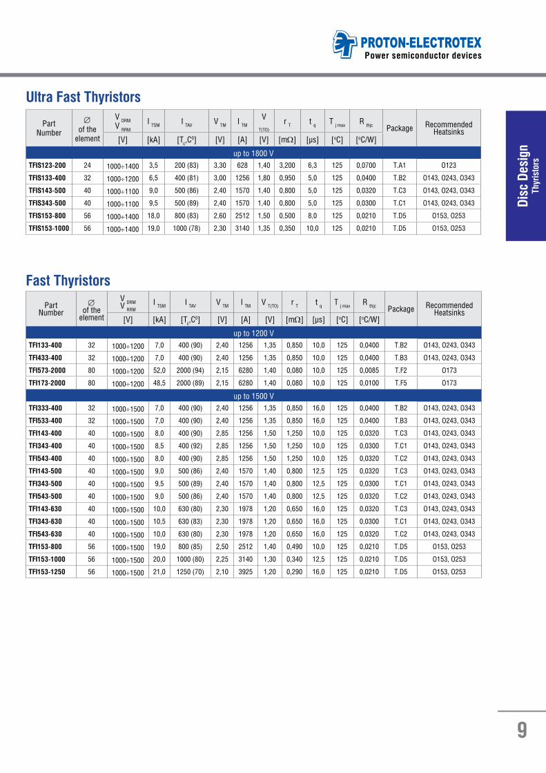
up to 1800 VTFIS123-200 24 1000÷1400 3,5 200 (83) 3,30 628 1,40 3,200 6,3 125 0,0700 T.A1 O123
TFIS133-400 32 1000÷1200 6,5 400 (81) 3,00 1256 1,80 0,950 5,0 125 0,0400 T.B2 O143, O243, O343
TFIS143-500 40 1000÷1100 9,0 500 (86) 2,40 1570 1,40 0,800 5,0 125 0,0320 T.C3 O143, O243, O343
TFIS343-500 40 1000÷1100 9,5 500 (89) 2,40 1570 1,40 0,800 5,0 125 0,0300 T.C1 O143, O243, O343
TFIS153-800 56 1000÷1400 18,0 800 (83) 2,60 2512 1,50 0,500 8,0 125 0,0210 T.D5 O153, O253
TFIS153-1000 56 1000÷1400 19,0 1000 (78) 2,30 3140 1,35 0,350 10,0 125 0,0210 T.D5 O153, O253
Ultra Fast Thyristors
Part Number
∅ of the
element
V DRMV RRMI TSM I TAV V TM I TM V T(TO) r T t q T j max R thjc Package Recommended
Heatsinks[V] [kA] [Тс,C
0] [V] [A] [V] [mΩ] [μs] [oC] [oC/W]
up to 1200 VTFI133-400 32 1000÷1200 7,0 400 (90) 2,40 1256 1,35 0,850 10,0 125 0,0400 T.B2 O143, O243, O343
TFI433-400 32 1000÷1200 7,0 400 (90) 2,40 1256 1,35 0,850 10,0 125 0,0400 T.B3 O143, O243, O343
TFI573-2000 80 1000÷1200 52,0 2000 (94) 2,15 6280 1,40 0,080 10,0 125 0,0085 T.F2 O173
TFI173-2000 80 1000÷1200 48,5 2000 (89) 2,15 6280 1,40 0,080 10,0 125 0,0100 T.F5 O173
up to 1500 VTFI333-400 32 1000÷1500 7,0 400 (90) 2,40 1256 1,35 0,850 16,0 125 0,0400 T.B2 O143, O243, O343
TFI533-400 32 1000÷1500 7,0 400 (90) 2,40 1256 1,35 0,850 16,0 125 0,0400 T.B3 O143, O243, O343
TFI143-400 40 1000÷1500 8,0 400 (90) 2,85 1256 1,50 1,250 10,0 125 0,0320 T.C3 O143, O243, O343
TFI343-400 40 1000÷1500 8,5 400 (92) 2,85 1256 1,50 1,250 10,0 125 0,0300 T.C1 O143, O243, O343
TFI543-400 40 1000÷1500 8,0 400 (90) 2,85 1256 1,50 1,250 10,0 125 0,0320 T.C2 O143, O243, O343
TFI143-500 40 1000÷1500 9,0 500 (86) 2,40 1570 1,40 0,800 12,5 125 0,0320 T.C3 O143, O243, O343
TFI343-500 40 1000÷1500 9,5 500 (89) 2,40 1570 1,40 0,800 12,5 125 0,0300 T.C1 O143, O243, O343
TFI543-500 40 1000÷1500 9,0 500 (86) 2,40 1570 1,40 0,800 12,5 125 0,0320 T.C2 O143, O243, O343
TFI143-630 40 1000÷1500 10,0 630 (80) 2,30 1978 1,20 0,650 16,0 125 0,0320 T.C3 O143, O243, O343
TFI343-630 40 1000÷1500 10,5 630 (83) 2,30 1978 1,20 0,650 16,0 125 0,0300 T.C1 O143, O243, O343
TFI543-630 40 1000÷1500 10,0 630 (80) 2,30 1978 1,20 0,650 16,0 125 0,0320 T.C2 O143, O243, O343
TFI153-800 56 1000÷1500 19,0 800 (85) 2,50 2512 1,40 0,490 10,0 125 0,0210 T.D5 O153, O253
TFI153-1000 56 1000÷1500 20,0 1000 (80) 2,25 3140 1,30 0,340 12,5 125 0,0210 T.D5 O153, O253
TFI153-1250 56 1000÷1500 21,0 1250 (70) 2,10 3925 1,20 0,290 16,0 125 0,0210 T.D5 O153, O253
Fast Thyristors
Disc
Des
ign
Thyr
isto
rs
10
You can find the Datasheets on our website www.proton-electrotex.com
Part Number
∅ of the
element
V DRMV RRMI TSM I TAV V TM I TM V T(TO) r T t q T j max R thjc Package Recommended
Heatsinks[V] [kA] [Тс,C
0] [V] [A] [V] [mΩ] [μs] [oC] [oC/W]
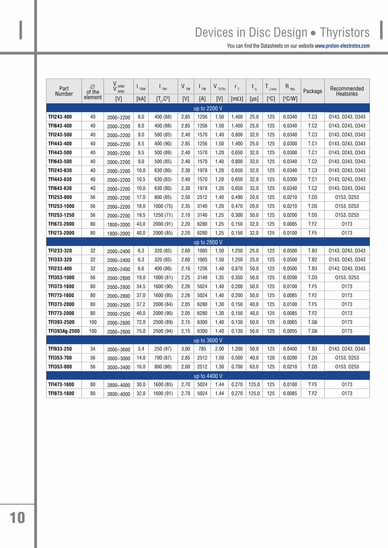
up to 2200 VTFI243-400 40 2000÷2200 8,0 400 (88) 2,85 1256 1,50 1,400 25,0 125 0,0340 T.C3 O143, O243, O343
TFI643-400 40 2000÷2200 8,0 400 (88) 2,85 1256 1,50 1,400 25,0 125 0,0340 T.C2 O143, O243, O343
TFI243-500 40 2000÷2200 9,0 500 (85) 2,40 1570 1,40 0,800 32,0 125 0,0340 T.C3 O143, O243, O343
TFI443-400 40 2000÷2200 8,5 400 (90) 2,85 1256 1,50 1,400 25,0 125 0,0300 T.C1 O143, O243, O343
TFI443-500 40 2000÷2200 9,5 500 (89) 2,40 1570 1,20 0,650 32,0 125 0,0300 T.C1 O143, O243, O343
TFI643-500 40 2000÷2200 9,0 500 (85) 2,40 1570 1,40 0,800 32,0 125 0,0340 T.C2 O143, O243, O343
TFI243-630 40 2000÷2200 10,0 630 (80) 2,30 1978 1,20 0,650 32,0 125 0,0340 T.C3 O143, O243, O343
TFI443-630 40 2000÷2200 10,5 630 (83) 2,40 1570 1,20 0,650 32,0 125 0,0300 T.C1 O143, O243, O343
TFI643-630 40 2000÷2200 10,0 630 (80) 2,30 1978 1,20 0,650 32,0 125 0,0340 T.C2 O143, O243, O343
TFI253-800 56 2000÷2200 17,0 800 (85) 2,50 2512 1,40 0,490 20,0 125 0,0210 T.D5 O153, O253
TFI253-1000 56 2000÷2200 18,0 1000 (75) 2,35 3140 1,20 0,470 20,0 125 0,0210 T.D5 O153, O253
TFI253-1250 56 2000÷2200 19,5 1250 (71) 2,10 3140 1,25 0,300 50,0 125 0,0200 T.D5 O153, O253
TFI673-2000 80 1800÷2000 43,0 2000 (91) 2,20 6280 1,25 0,150 32,0 125 0,0085 T.F2 O173
TFI273-2000 80 1800÷2000 40,0 2000 (85) 2,20 6280 1,25 0,150 32,0 125 0,0100 T.F5 O173
up to 2800 VTFI233-320 32 2000÷2400 6,3 320 (85) 2,60 1005 1,50 1,250 25,0 125 0,0500 T.B3 O143, O243, O343
TFI333-320 32 2000÷2400 6,3 320 (85) 2,60 1005 1,50 1,250 25,0 125 0,0500 T.B2 O143, O243, O343
TFI233-400 32 2000÷2400 6,6 400 (80) 2,10 1256 1,40 0,870 50,0 125 0,0500 T.B3 O143, O243, O343
TFI353-1000 56 2000÷2800 19,0 1000 (81) 2,25 3140 1,35 0,350 50,0 125 0,0200 T.D5 O153, O253
TFI373-1600 80 2000÷2800 34,5 1600 (90) 2,26 5024 1,40 0,200 50,0 125 0,0100 T.F5 O173
TFI773-1600 80 2000÷2800 37,0 1600 (95) 2,26 5024 1,40 0,200 50,0 125 0,0085 T.F2 O173
TFI373-2000 80 2000÷2500 37,2 2000 (84) 2,05 6280 1,30 0,150 40,0 125 0,0100 T.F5 O173
TFI773-2000 80 2000÷2500 40,0 2000 (90) 2,05 6280 1,30 0,150 40,0 125 0,0085 T.F2 O173
TFI393-2500 100 2000÷2800 72,0 2500 (89) 2,15 6300 1,40 0,130 50,0 125 0,0065 T.G6 О173
TFI393Ag-2500 100 2000÷2800 75,0 2500 (94) 2,15 6300 1,40 0,130 50,0 125 0,0055 T.G6 О173
up to 3600 VTFI933-250 34 3000÷3600 5,4 250 (97) 3,00 785 2,00 1,200 50,0 125 0,0400 T.B3 O143, O243, O343
TFI353-700 56 3000÷3000 14,0 700 (87) 2,85 2512 1,50 0,500 40,0 120 0,0200 T.D5 O153, O253
TFI353-800 56 3000÷3400 16,0 800 (80) 2,60 2512 1,30 0,700 63,0 125 0,0210 T.D5 O153, O253
up to 4400 VTFI473-1600 80 3800÷4000 30,0 1600 (85) 2,70 5024 1,44 0,270 125,0 125 0,0100 T.F5 O173
TFI873-1600 80 3800÷4000 32,0 1600 (91) 2,70 5024 1,44 0,270 125,0 125 0,0085 T.F2 O173
IDevices in Disc Design • ThyristorsI

11
Power semiconductor devices
T.A1 T.B2
T.B3
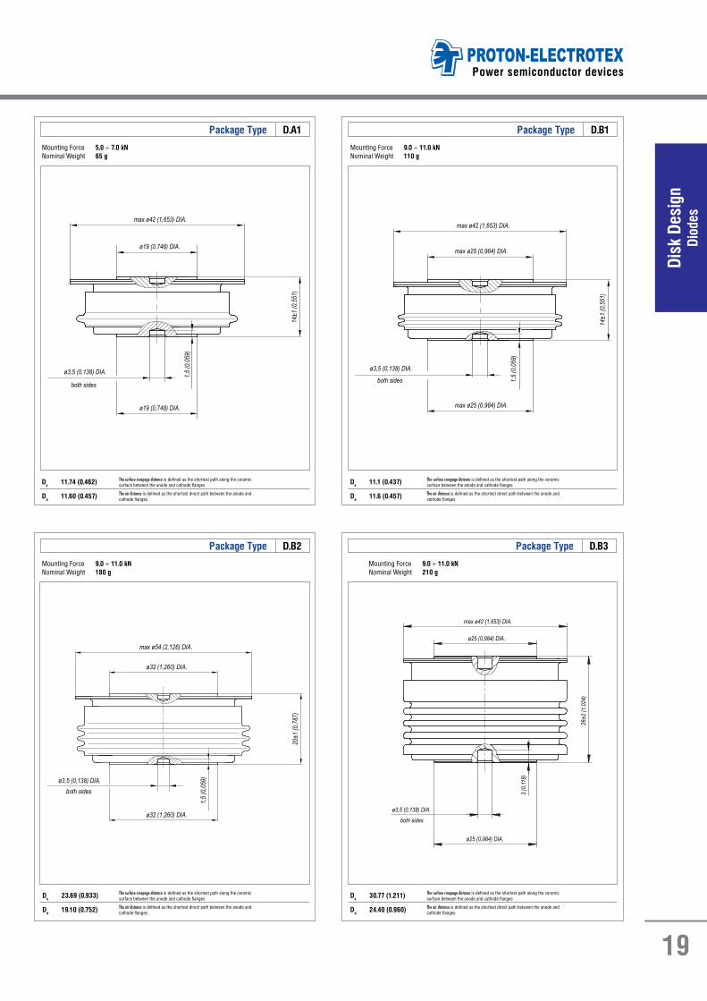
Package Type Package Type
Package Type
Mounting Force 5.0 ÷ 7.0 kNNominal Weight 70 g
Mounting Force 9.0 ÷ 11.0 kNNominal Weight 110 g
Mounting Force 9.0 ÷ 11.0 kNNominal Weight 180 g
Ds 7.94 (0.313) Ds 10.3 (0.405)
Ds 19.44 (0.765)
The surface creepage distance is defined as the shortest path along the ceramic surface between the anode and cathode flanges
The surface creepage distance is defined as the shortest path along the ceramic surface between the anode and cathode flanges
The surface creepage distance is defined as the shortest path along the ceramic surface between the anode and cathode flanges
The air distance is defined as the shortest direct path between the anode and cathode flanges
The air distance is defined as the shortest direct path between the anode and cathode flanges
The air distance is defined as the shortest direct path between the anode and cathode flangesDa 5.00 (0.197) Da 6.3 (0.248)
Da 12.10 (0.476)
I
Disc
Des
ign
Thyr
isto
rs
12
You can find the Datasheets on our website www.proton-electrotex.com
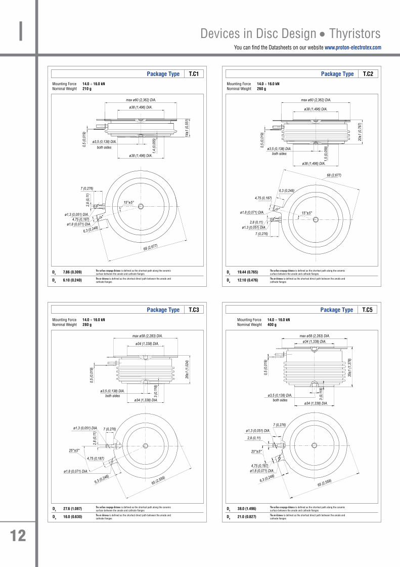
T.C1Package Type
Mounting Force 14.0 ÷ 16.0 kNNominal Weight 210 g
Ds 7.86 (0.309) The surface creepage distance is defined as the shortest path along the ceramic surface between the anode and cathode flanges
The air distance is defined as the shortest direct path between the anode and cathode flangesDa 6.10 (0.240)
T.C2Package Type
Mounting Force 14.0 ÷ 16.0 kNNominal Weight 260 g
Ds 19.44 (0.765) The surface creepage distance is defined as the shortest path along the ceramic surface between the anode and cathode flanges
The air distance is defined as the shortest direct path between the anode and cathode flangesDa 12.10 (0.476)
T.C3Package Type
Mounting Force 14.0 ÷ 16.0 kNNominal Weight 280 g
Ds 27.6 (1.087) The surface creepage distance is defined as the shortest path along the ceramic surface between the anode and cathode flanges
The air distance is defined as the shortest direct path between the anode and cathode flangesDa 16.0 (0.630)
T.C5Package Type
Mounting Force 14.0 ÷ 16.0 kNNominal Weight 400 g
Ds 38.0 (1.496) The surface creepage distance is defined as the shortest path along the ceramic surface between the anode and cathode flanges
The air distance is defined as the shortest direct path between the anode and cathode flangesDa 21.0 (0.827)
Devices in Disc Design • ThyristorsI

13
Power semiconductor devices
T.C6Package Type
Mounting Force 14.0 ÷ 16.0 kNNominal Weight 280 g
Ds 29.6 (1.165) The surface creepage distance is defined as the shortest path along the ceramic surface between the anode flange and the gate contact
The air distance is defined as the shortest direct path between the anode flange and gate contactDa 18.25 (0.716)
T.D1Package Type
Mounting Force 24.0 ÷ 28.0 kNNominal Weight 330 g
Ds 7.51 (0.295) The surface creepage distance is defined as the shortest path along the ceramic surface between the anode and cathode flanges
The air distance is defined as the shortest direct path between the anode and cathode flangesDa 5.60 (0.220)
T.D5Package Type
Mounting Force 24.0 ÷ 28.0 kNNominal Weight 510 g
Ds 30.38 (1.196) The surface creepage distance is defined as the shortest path along the ceramic surface between the anode and cathode flanges
The air distance is defined as the shortest direct path between the anode and cathode flangesDa 18.05 (0.710)
T.D4Package Type
Mounting Force 24.0 ÷ 28.0 kNNominal Weight 700 g
Ds 39.55 (1.557) The surface creepage distance is defined as the shortest path along the ceramic surface between the anode and cathode flanges
The air distance is defined as the shortest direct path between the anode and cathode flangesDa 25.50 (1.004)
Disc
Des
ign
Thyr
isto
rs
PROTON-ELECTROTEX
All dimensions in millimeters (inches)
Package Type T.C6 Mounting Force 14.0 ÷ 16.0 kN Nominal Weight 280 g
Ds 29.6 (1.165) The surface creepage distance is defined as the shortest path along the ceramic surface between the anode flange and the gate contact
Da 18.25 (0.716) The air distance is defined as the shortest direct path between the anode flange and gate contact

14
You can find the Datasheets on our website www.proton-electrotex.com
T.E3Package Type
Mounting Force 33.0 ÷ 40.0 kNNominal Weight 1000 g
Ds 36.50 (1.437) The surface creepage distance is defined as the shortest path along the ceramic surface between the anode and cathode flanges
The air distance is defined as the shortest direct path between the anode and cathode flangesDa 16.50 (0.650)
T.E4Package Type
Mounting Force 33.0 ÷ 40.0 kNNominal Weight 1200 g
Ds 43.80 (1.724) The surface creepage distance is defined as the shortest path along the ceramic surface between the anode and cathode flanges
The air distance is defined as the shortest direct path between the anode and cathode flangesDa 25.50 (1.004)
T.F2Package Type
Mounting Force 40.0 ÷ 50.0 kNNominal Weight 1500 g
Ds 36.6 (1.441) The surface creepage distance is defined as the shortest path along the ceramic surface between the anode and cathode flanges
The air distance is defined as the shortest direct path between the anode and cathode flangesDa 16.2 (0.638)
T.F5Package Type
Mounting Force 40.0 ÷ 50.0 kNNominal Weight 1700 g
Ds 47.12 (1.855) The surface creepage distance is defined as the shortest path along the ceramic surface between the anode and cathode flanges
The air distance is defined as the shortest direct path between the anode and cathode flangesDa 25.40 (1.000)
Devices in Disc Design • ThyristorsI

15
Power semiconductor devices
Disc
Des
ign
Thyr
isto
rs
T.G5Package Type
Mounting Force 70.0 ÷ 90.0 kNNominal Weight 2200 g
Ds 44.60 (1.756) The surface creepage distance is defined as the shortest path along the ceramic surface between the anode and cathode flanges
The air distance is defined as the shortest direct path between the anode and cathode flangesDa 15.70 (0.618)
T.G6Package Type
Mounting Force 70.0 ÷ 90.0 kNNominal Weight 2700 g
Ds 62.09 (2.444) The surface creepage distance is defined as the shortest path along the ceramic surface between the anode and cathode flanges
The air distance is defined as the shortest direct path between the anode and cathode flangesDa 23.40 (0.921)
T.H1Package Type
Mounting Force 60.0 ÷ 70.0 kNNominal Weight 1900 g
Ds 36.50 (1.437) The surface creepage distance is defined as the shortest path along the ceramic surface between the anode and cathode flanges
The air distance is defined as the shortest direct path between the anode and cathode flangesDa 16.50 (0.650)
T.H2Package Type
Mounting Force 60.0 ÷ 70.0 kNNominal Weight 2200 g
Ds 45.40 (1.787) The surface creepage distance is defined as the shortest path along the ceramic surface between the anode and cathode flanges
The air distance is defined as the shortest direct path between the anode and cathode flangesDa 25.50 (1.004)
16
You can find the Datasheets on our website www.proton-electrotex.com
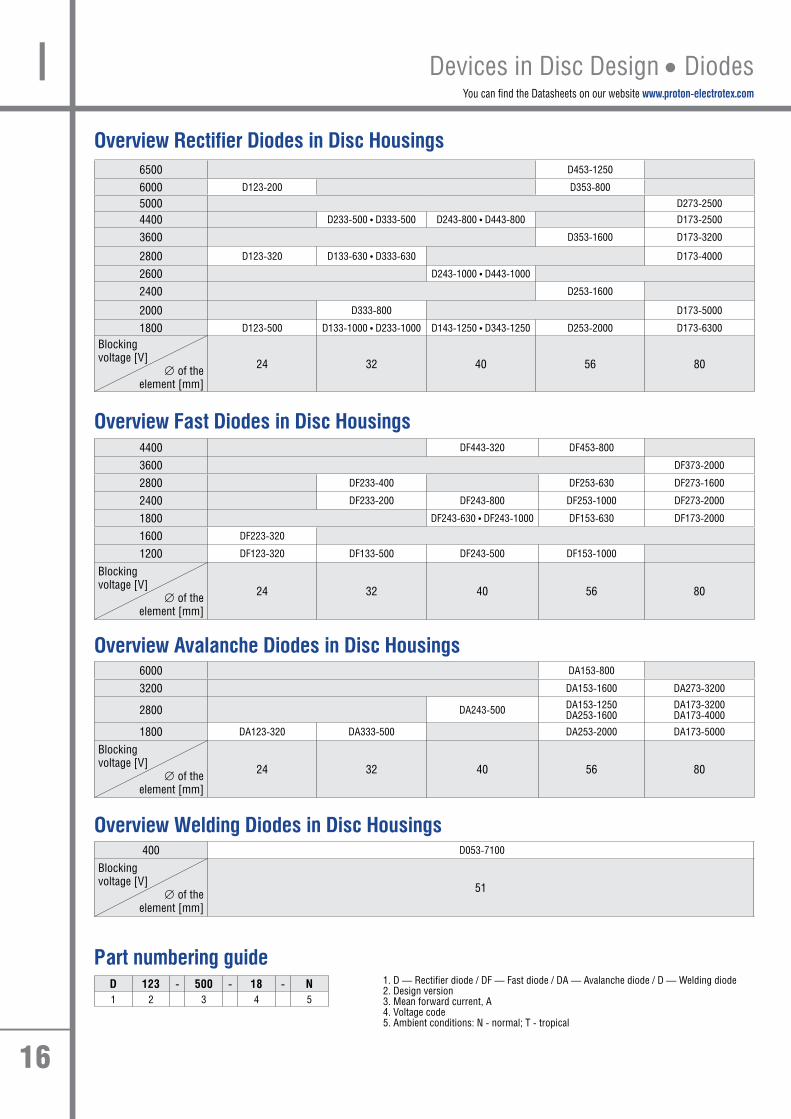
6500 D453-1250
6000 D123-200 D353-800
5000 D273-2500
4400 D233-500 • D333-500 D243-800 • D443-800 D173-2500
3600 D353-1600 D173-3200
2800 D123-320 D133-630 • D333-630 D173-4000
2600 D243-1000 • D443-1000
2400 D253-1600
2000 D333-800 D173-5000
1800 D123-500 D133-1000 • D233-1000 D143-1250 • D343-1250 D253-2000 D173-6300
Blockingvoltage [V]
∅ of the element [mm]
24 32 40 56 80
4400 DF443-320 DF453-800
3600 DF373-2000
2800 DF233-400 DF253-630 DF273-1600
2400 DF233-200 DF243-800 DF253-1000 DF273-2000
1800 DF243-630 • DF243-1000 DF153-630 DF173-2000
1600 DF223-320
1200 DF123-320 DF133-500 DF243-500 DF153-1000
Blockingvoltage [V]
∅ of the element [mm]
24 32 40 56 80
6000 DA153-800
3200 DA153-1600 DA273-3200
2800 DA243-500 DA153-1250DA253-1600
DA173-3200DA173-4000
1800 DA123-320 DA333-500 DA253-2000 DA173-5000
Blockingvoltage [V]
∅ of the element [mm]
24 32 40 56 80
400 D053-7100
Blockingvoltage [V]
∅ of the element [mm]
51
Overview Rectifier Diodes in Disc Housings
Overview Fast Diodes in Disc Housings
Overview Avalanche Diodes in Disc Housings
Overview Welding Diodes in Disc Housings
D 123 - 500 - 18 - N1 2 3 4 5
Part numbering guide1. D — Rectifier diode / DF — Fast diode / DA — Avalanche diode / D — Welding diode2. Design version3. Mean forward current, A4. Voltage code5. Ambient conditions: N - normal; T - tropical
Devices in Disc Design • DiodesI

17
Power semiconductor devices
Disk
Des
ign
Diod
es
Part Number
∅ of the
element
V RRM I FSM I FAV V FM I FM
V F (TO)T j max
r T T j max R thjc Package RecommendedHeatsinks
[V] [kA] [Тс,C0] [V] [A] [V] [mΩ] [oC] [oC/W]
D053-7100 51 200÷400 55,0 7100 (84,5) 1,05 5000 0,70 0,029 170 0,0100 D.H1 –
Welding Diodes
Part Number
∅ of the
element
V RRM I FSM I FAV V FM I FM
V F (TO)T j max
r T T j max R thjc Package RecommendedHeatsinks
[V] [kA] [Тс,C0] [V] [A] [V] [mΩ] [oC] [oC/W]
up to 1800 VD123-500 24 1000÷1800 7,5 500 (137) 1,55 1570 0,90 0,500 190 0,0700 D.A1 O123
D133-1000 32 1000÷1800 15,0 1000 (117) 1,55 3140 0,95 0,350 190 0,0400 D.B1 O143, O243, O343
D233-1000 32 1000÷1800 16,0 1000 (117) 1,55 3140 0,95 0,350 190 0,0400 D.B2 O143, O243, O343
D143-1250 40 1000÷1800 22,0 1250 (121) 1,65 3925 0,95 0,250 190 0,0320 D.C2 O143, O243, O343
D343-1250 40 1000÷1800 20,0 1250 (114) 1,65 3925 0,95 0,250 190 0,0350 D.C3 O143, O243, O343
D253-2000 56 1000÷1800 35,0 2000 (138) 1,55 6280 0,95 0,100 190 0,0180 D.D3 O153, O253
D173-6300 80 1000÷1800 76,0 6300 (102) 1,30 12560 0,70 0,043 175 0,0085 D.F1 O173
up to 2800 VD123-320 24 2000÷2800 5,5 320 (135) 2,00 1005 1,00 1,000 175 0,0700 D.A1 O123
D133-630 32 2000÷2800 12,0 630 (133) 1,60 1978 1,10 0,350 175 0,0400 D.B2 O143, O243, O343
D333-630 32 2000÷2800 10,0 630 (128) 1,60 1978 1,10 0,350 175 0,0450 D.B3 O143, O243, O343
D333-800 32 1800÷2000 12,0 800 (134) 1,60 2512 1,00 0,270 190 0,0450 D.B3 O143, O243, O343
D243-1000 40 2000÷2600 19,0 1000 (122) 1,65 3140 0,95 0,280 175 0,0320 D.C2 O143, O243, O343
D443-1000 40 2000÷2600 18,0 1000 (117) 1,65 3140 0,95 0,280 175 0,0350 D.C3 O143, O243, O343
D253-1600 56 2000÷2400 35,0 1600 (147) 1,50 5024 1,00 0,120 190 0,0180 D.D3 O153, O253
D173-4000 80 2000÷2800 55,0 4000 (124) 1,80 12560 0,85 0,065 175 0,0085 D.F1 O173
D173-5000 80 2000 60,0 5000 (109) 1,65 12560 0,75 0,650 175 0,0085 D.F1 O173
up to 3600 VD353-1600 56 3000÷3600 26,0 1600 (133) 2,00 5024 0,85 0,150 175 0,0180 D.D3 O153, O253
D173-3200 80 3000÷3600 50,0 3200 (109) 1,80 10048 1,25 0,080 160 0,0085 D.F1 O173
up to 4400 VD233-500 32 3800÷4400 7,5 500 (106) 2,00 1570 1,05 0,900 150 0,0400 D.B2 O143, O243, O343
D333-500 32 3800÷4400 6,5 500 (101) 2,00 1570 1,05 0,900 150 0,0450 D.B3 O143, O243, O343
D243-800 40 3800÷4400 13,5 800 (99) 1,95 2512 1,00 0,500 150 0,0320 D.C2 O143, O243, O343
D443-800 40 3800÷4400 12,5 800 (94) 1,95 2512 1,00 0,500 150 0,0350 D.C3 O143, O243, O343
D173-2500 80 3800÷4400 40,0 2500 (116) 1,80 7850 0,80 0,125 150 0,0085 D.F1 O173
up to 6500 VD123-200 24 4600÷6000 3,0 200 (116) 2,50 628 1,10 2,600 150 0,0700 D.A1 O123
D353-800 56 4600÷6000 12,0 800 (100) 2,40 2512 1,31 0,740 140 0,0180 D.D3 O143, O243, O343
D453-1250 56 4600÷6500 18,0 1250 (101) 2,40 3925 0,95 0,400 150 0,0180 D.D3 O143, O243, O343
D273-2500 80 4600÷5000 40,0 2500 (112) 1,90 7850 0,85 0,150 150 0,0085 D.F1 O173
Rectifier Diodes

18
You can find the Datasheets on our website www.proton-electrotex.com
Devices in Disc Design • DiodesI
Part Number
∅ of the
element
V RRM I FSM I FAV V FM I FM
V F (TO)T j max
r T t rr T j max R thjc Package RecommendedHeatsinks
[V] [kA] [Тс,C0] [V] [A] [V] [mΩ] [μs] [oC] [oC/W]
up to 1800 VDF123-320 24 1000÷1200 6,0 320 (108) 1,70 1005 1,20 0,850 3,2 150 0,0700 D.A1 O123
DF223-320 24 1000÷1600 5,0 320 (102) 2,20 1005 1,25 1,100 2,5 150 0,0700 D.A1 O123
DF133-500 32 1000÷1200 8,5 500 (91) 2,20 1570 1,25 0,350 2,5 125 0,0400 D.B1 O143, O243, O343
DF243-500 40 1000÷1200 12,0 500 (97) 2,30 1570 1,25 0,400 2,0 125 0,0320 D.C2 O143, O243, O343
DF243-630 40 1000÷1800 14,0 630 (91) 2,30 1978 1,20 0,300 3,2 125 0,0320 D.C2 O143, O243, O343
DF243-1000 40 1000÷1800 15,0 1000 (68) 1,80 3140 1,15 0,250 5,0 125 0,0320 D.C2 O143, O243, O343
DF153-630 56 1000÷1800 25,0 630 (105) 3,00 1978 1,25 0,300 2,5 125 0,0180 D.D3 O153, O253
DF153-1000 56 1000÷1200 29,0 1000 (95) 1,90 3140 1,15 0,200 2,5 125 0,0180 D.D3 O153, O253
DF173-2000 80 1000÷1800 50,0 2000 (93) 1,80 6280 1,20 0,130 6,3 125 0,0085 D.F1 O173
up to 2800 VDF233-200 32 2000÷2400 6,0 200 (107) 2,20 628 1,35 1,700 1,25 125 0,0400 D.B2 O143, O243, O343
DF233-400 32 2000÷2800 7,0 400 (94) 1,90 1256 1,20 0,700 5,0 125 0,0400 D.B2 O143, O243, O343
DF243-800 40 2000÷2400 12,5 800 (74) 2,20 2512 1,30 0,350 4,0 125 0,0320 D.C2 O143, O243, O343
DF253-630 56 2000÷2800 20,0 630 (103) 3,00 1978 1,35 0,350 3,2 125 0,0180 D.D3 O153, O253
DF253-1000 56 2000÷2400 22,0 1000 (89) 2,20 3140 1,35 0,250 4,0 125 0,0180 D.D3 O153, O253
DF273-1600 80 2000÷2800 44,0 1600 (98) 2,10 5024 1,30 0,170 8,0 125 0,0085 D.F1 O173
DF273-2000 80 2000÷2400 46,0 2000 (90) 1,85 6280 1,30 0,150 8,0 125 0,0085 D.F1 O173
up to 3600 VDF373-2000 80 3000÷3600 40,0 2000 (84) 2,10 6280 1,40 0,200 16,0 125 0,0085 D.F1 O173
up to 4400 VDF443-320 40 3800÷4400 6,0 320 (90) 3,60 1000 1,50 2,000 4,0 125 0,0350 D.C3 O143, O243, O343
DF453-800 56 3800÷4400 13,5 800 (85) 2,90 2512 1,40 0,700 5,3 125 0,0180 D.D3 O153, O253
Fast Diodes
Part Number
∅ of the
element
V RRM I FSM I FAV V FM I FM
V F (TO)T j max
r T T j max R thjc Package RecommendedHeatsinks
[V] [kA] [Тс,C0] [V] [A] [V] [mΩ] [oC] [oC/W]
up to 1800 VDA123-320 24 1000÷1800 5,5 320 (110) 1,60 1005 0,95 1,050 150 0,0700 D.A1 O123
DA333-500 32 1000÷1800 12,0 500 (120) 1,60 1570 0,95 0,440 150 0,0400 D.B2 O143, O243, O343
DA253-2000 56 1000÷1800 30,0 2000 (101) 2,00 6280 0,95 0,220 175 0,0180 D.D3 O153, O253
DA173-5000 80 1000÷1800 60,0 5000 (84) 2,00 12560 0,60 0,125 175 0,0085 D.F1 O173
up to 2800 VDA243-500 40 2000÷2800 13,0 500 (118) 2,00 1570 1,00 0,800 150 0,0320 D.C2 O143, O243, O343
DA153-1250 56 2000÷2800 22,0 1250 (121) 2,20 3925 1,00 0,450 175 0,0180 D.D3 O153, O253
DA253-1600 56 2000÷2800 25,0 1600 (112) 2,10 5024 1,00 0,300 175 0,0180 D.D3 O153, O253
DA173-3200 80 2000÷2800 47,0 3200 (115) 2,00 10048 1,00 0,150 175 0,0085 D.F1 O173
DA173-4000 80 2000÷2800 50,0 4000 (107) 2,20 12560 1,00 0,100 175 0,0085 D.F1 O173
up to 3600 V
DA153-1600 56 2400÷3200 27,0 1600 (111) 2,00 5024 0,95 0,320 175 0,0180 D.D3 O153, O253
DA273-3200 80 3000÷3600 42,0 3200 (103) 2,20 10048 1,05 0,200 175 0,0085 D.F1 O173
up to 6000 V
DA153-800 56 4600÷6000 14,0 800 (108) 2,20 2512 0,90 0,650 140 0,0180 D.D3 O153, O253
Avalanche Diodes
19
Power semiconductor devices
Disk
Des
ign
Diod
es
D.A1 D.B1
D.B2 D.B3
Package Type Package Type
Package Type Package Type
Mounting Force 5.0 ÷ 7.0 kNNominal Weight 65 g
Mounting Force 9.0 ÷ 11.0 kNNominal Weight 110 g
Mounting Force 9.0 ÷ 11.0 kNNominal Weight 180 g
Mounting Force 9.0 ÷ 11.0 kNNominal Weight 210 g
Ds 11.74 (0.462) Ds 11.1 (0.437)
Ds 23.69 (0.933) Ds 30.77 (1.211)
The surface creepage distance is defined as the shortest path along the ceramic surface between the anode and cathode flanges
The surface creepage distance is defined as the shortest path along the ceramic surface between the anode and cathode flanges
The surface creepage distance is defined as the shortest path along the ceramic surface between the anode and cathode flanges
The surface creepage distance is defined as the shortest path along the ceramic surface between the anode and cathode flanges
The air distance is defined as the shortest direct path between the anode and cathode flanges
The air distance is defined as the shortest direct path between the anode and cathode flanges
The air distance is defined as the shortest direct path between the anode and cathode flanges
The air distance is defined as the shortest direct path between the anode and cathode flanges
Da 11.60 (0.457) Da 11.6 (0.457)
Da 19.10 (0.752) Da 24.40 (0.960)

20
You can find the Datasheets on our website www.proton-electrotex.com
D.C2 D.C3Package Type Package Type
Mounting Force 14.0 ÷ 16.0 kNNominal Weight 260 g
Mounting Force 14.0 ÷ 16.0 kNNominal Weight 280 g
Ds 23.69 (0.933) Ds 33.3 (1.311)The surface creepage distance is defined as the shortest path along the ceramic surface between the anode and cathode flanges
The surface creepage distance is defined as the shortest path along the ceramic surface between the anode and cathode flanges
The air distance is defined as the shortest direct path between the anode and cathode flanges
The air distance is defined as the shortest direct path between the anode and cathode flangesDa 19.10 (0.752) Da 22.5 (0.886)
D.D3Package Type
Mounting Force 24.0 ÷ 28.0 kNNominal Weight 510 g
Ds 38.84 (1.529) The surface creepage distance is defined as the shortest path along the ceramic surface between the anode and cathode flanges
The air distance is defined as the shortest direct path between the anode and cathode flangesDa 22.50 (0.886)
Devices in Disc Design • DiodesI
D.F1Package Type
Mounting Force 40.0 ÷ 50.0 kNNominal Weight 1500 g
Ds 41.4 (1.630) The surface creepage distance is defined as the shortest path along the ceramic surface between the anode and cathode flanges
The air distance is defined as the shortest direct path between the anode and cathode flangesDa 23.1 (0.909)
21
Power semiconductor devices
Disk
Des
ign
Diod
es
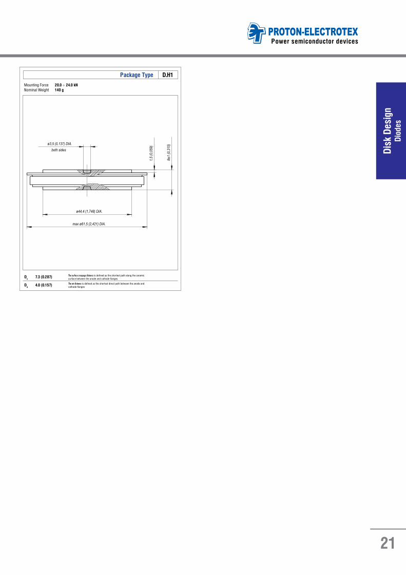
D.H1Package Type
Mounting Force 20.0 ÷ 24.0 kNNominal Weight 140 g
Ds 7.3 (0.287) The surface creepage distance is defined as the shortest path along the ceramic surface between the anode and cathode flanges
The air distance is defined as the shortest direct path between the anode and cathode flangesDa 4.0 (0.157)

Main Characteristics:• Mean on-state and forward currents up to 500 А.• Blocking voltage up to 1800 V.• Pressure contact construction. • Simple mounting. • High resistance to cyclic load.• Diodes can be supplied with direct and reverse polarity.• Metric and inch thread.
Optional opportunities:• Selection of devices in groups for parallel, series and combined connection. • Delivery of devices assembled with heat sinks.
Application:Devices in stud design are applied in railway transport: rectifier bridges, AC control, electric motor drive for industry and transport.
PART IIDevices in Stud Design
23
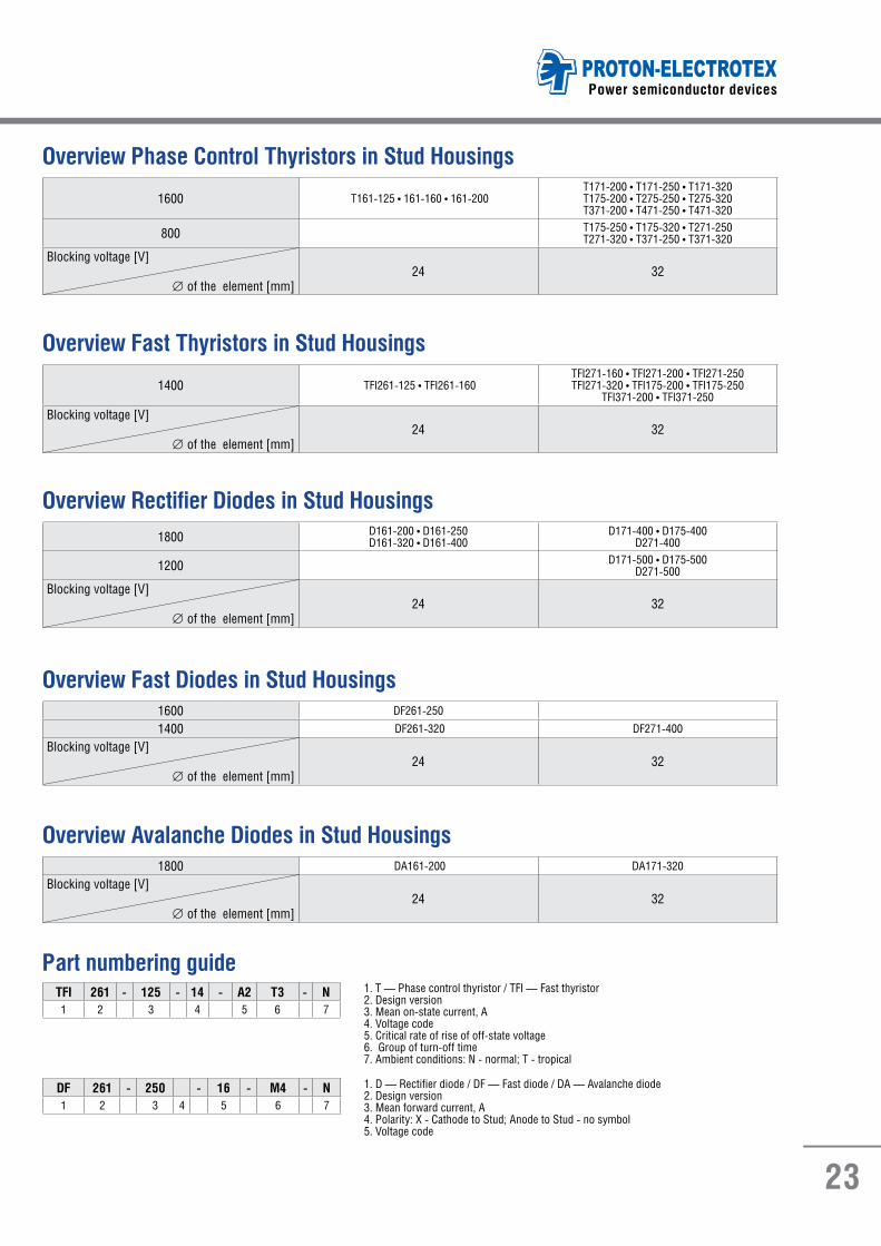
Power semiconductor devices
1600 T161-125 • 161-160 • 161-200Т171-200 • T171-250 • T171-320Т175-200 • Т275-250 • T275-320 Т371-200 • Т471-250 • T471-320
800 Т175-250 • T175-320 • Т271-250 T271-320 • Т371-250 • T371-320
Blocking voltage [V]
∅ of the element [mm]24 32
1800 D161-200 • D161-250 D161-320 • D161-400
D171-400 • D175-400D271-400
1200 D171-500 • D175-500D271-500
Blocking voltage [V]
∅ of the element [mm]24 32
1600 DF261-250
1400 DF261-320 DF271-400
Blocking voltage [V]
∅ of the element [mm]24 32
1800 DA161-200 DA171-320
Blocking voltage [V]
∅ of the element [mm]24 32
1400 TFI261-125 • TFI261-160TFI271-160 • TFI271-200 • TFI271-250TFI271-320 • TFI175-200 • TFI175-250
TFI371-200 • TFI371-250
Blocking voltage [V]
∅ of the element [mm]24 32
Overview Phase Control Thyristors in Stud Housings
Overview Rectifier Diodes in Stud Housings
Overview Fast Diodes in Stud Housings
Overview Avalanche Diodes in Stud Housings
Overview Fast Thyristors in Stud Housings
TFI 261 - 125 - 14 - A2 T3 - N1 2 3 4 5 6 7
DF 261 - 250 - 16 - M4 - N1 2 3 4 5 6 7
Part numbering guide1. T — Phase control thyristor / TFI — Fast thyristor 2. Design version3. Mean on-state current, A4. Voltage code5. Critical rate of rise of off-state voltage6. Group of turn-off time7. Ambient conditions: N - normal; T - tropical
1. D — Rectifier diode / DF — Fast diode / DA — Avalanche diode2. Design version3. Mean forward current, A4. Polarity: X - Cathode to Stud; Anode to Stud - no symbol5. Voltage code
24
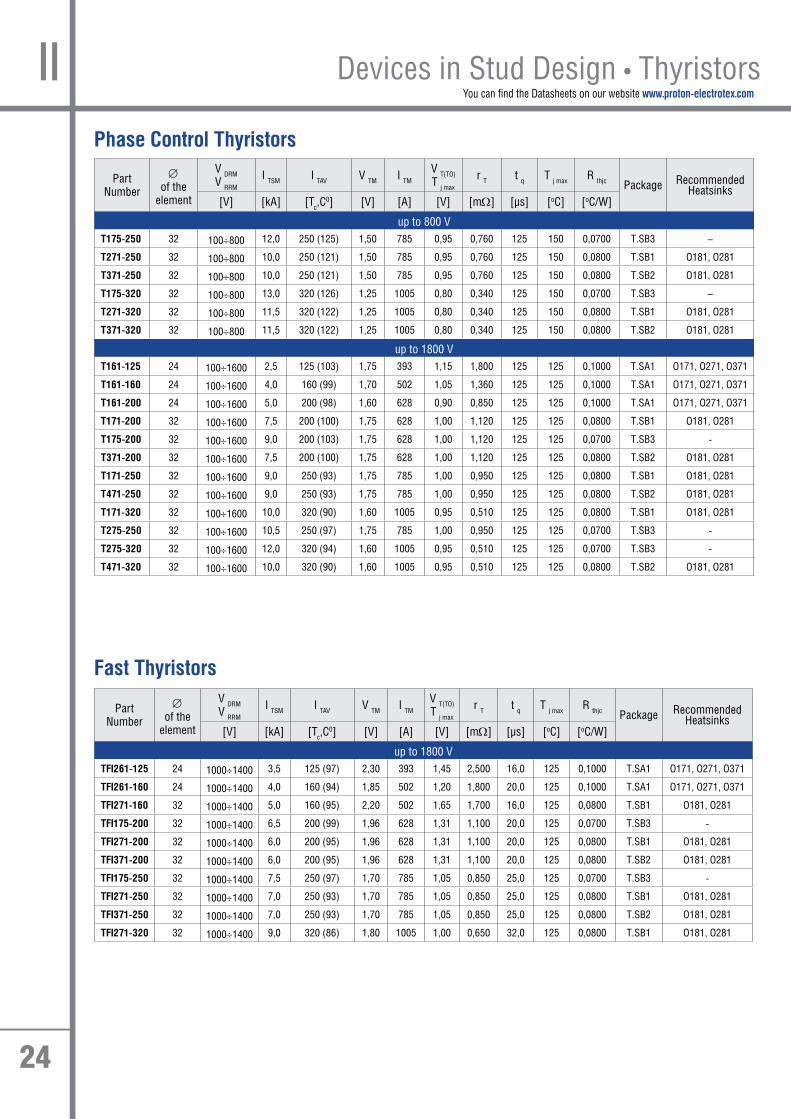
You can find the Datasheets on our website www.proton-electrotex.com
Part Number
∅ of the
element
V DRMV RRM I TSM I TAV V TM I TM
V T(TO)T j max
r T t q T j max R thjc Package RecommendedHeatsinks
[V] [kA] [Тс,C0] [V] [A] [V] [mΩ] [μs] [oC] [oC/W]
up to 800 V T175-250 32 100÷800 12,0 250 (125) 1,50 785 0,95 0,760 125 150 0,0700 T.SB3 –
T271-250 32 100÷800 10,0 250 (121) 1,50 785 0,95 0,760 125 150 0,0800 T.SB1 O181, O281
T371-250 32 100÷800 10,0 250 (121) 1,50 785 0,95 0,760 125 150 0,0800 T.SB2 O181, O281
T175-320 32 100÷800 13,0 320 (126) 1,25 1005 0,80 0,340 125 150 0,0700 T.SB3 –
T271-320 32 100÷800 11,5 320 (122) 1,25 1005 0,80 0,340 125 150 0,0800 T.SB1 O181, O281
T371-320 32 100÷800 11,5 320 (122) 1,25 1005 0,80 0,340 125 150 0,0800 T.SB2 O181, O281
up to 1800 V T161-125 24 100÷1600 2,5 125 (103) 1,75 393 1,15 1,800 125 125 0,1000 T.SA1 O171, O271, O371
T161-160 24 100÷1600 4,0 160 (99) 1,70 502 1,05 1,360 125 125 0,1000 T.SA1 O171, O271, O371
T161-200 24 100÷1600 5,0 200 (98) 1,60 628 0,90 0,850 125 125 0,1000 T.SA1 O171, O271, O371
T171-200 32 100÷1600 7,5 200 (100) 1,75 628 1,00 1,120 125 125 0,0800 T.SB1 O181, O281
T175-200 32 100÷1600 9,0 200 (103) 1,75 628 1,00 1,120 125 125 0,0700 T.SB3 -
T371-200 32 100÷1600 7,5 200 (100) 1,75 628 1,00 1,120 125 125 0,0800 T.SB2 O181, O281
T171-250 32 100÷1600 9,0 250 (93) 1,75 785 1,00 0,950 125 125 0,0800 T.SB1 O181, O281
T471-250 32 100÷1600 9,0 250 (93) 1,75 785 1,00 0,950 125 125 0,0800 T.SB2 O181, O281
T171-320 32 100÷1600 10,0 320 (90) 1,60 1005 0,95 0,510 125 125 0,0800 T.SB1 O181, O281
T275-250 32 100÷1600 10,5 250 (97) 1,75 785 1,00 0,950 125 125 0,0700 T.SB3 -
T275-320 32 100÷1600 12,0 320 (94) 1,60 1005 0,95 0,510 125 125 0,0700 T.SB3 -
T471-320 32 100÷1600 10,0 320 (90) 1,60 1005 0,95 0,510 125 125 0,0800 T.SB2 O181, O281
Part Number
∅ of the
element
V DRM V RRM
I TSM I TAV V TM I TM
V T(TO)T j max
r T t q T j max R thjc Package RecommendedHeatsinks
[V] [kA] [Тс,C0] [V] [A] [V] [mΩ] [μs] [oC] [oC/W]
up to 1800 V TFI261-125 24 1000÷1400 3,5 125 (97) 2,30 393 1,45 2,500 16,0 125 0,1000 T.SA1 O171, O271, O371
TFI261-160 24 1000÷1400 4,0 160 (94) 1,85 502 1,20 1,800 20,0 125 0,1000 T.SA1 O171, O271, O371
TFI271-160 32 1000÷1400 5,0 160 (95) 2,20 502 1,65 1,700 16,0 125 0,0800 T.SB1 O181, O281
TFI175-200 32 1000÷1400 6,5 200 (99) 1,96 628 1,31 1,100 20,0 125 0,0700 T.SB3 -
TFI271-200 32 1000÷1400 6,0 200 (95) 1,96 628 1,31 1,100 20,0 125 0,0800 T.SB1 O181, O281
TFI371-200 32 1000÷1400 6,0 200 (95) 1,96 628 1,31 1,100 20,0 125 0,0800 T.SB2 O181, O281
TFI175-250 32 1000÷1400 7,5 250 (97) 1,70 785 1,05 0,850 25,0 125 0,0700 T.SB3 -
TFI271-250 32 1000÷1400 7,0 250 (93) 1,70 785 1,05 0,850 25,0 125 0,0800 T.SB1 O181, O281
TFI371-250 32 1000÷1400 7,0 250 (93) 1,70 785 1,05 0,850 25,0 125 0,0800 T.SB2 O181, O281
TFI271-320 32 1000÷1400 9,0 320 (86) 1,80 1005 1,00 0,650 32,0 125 0,0800 T.SB1 O181, O281
Phase Control Thyristors
Fast Thyristors
Devices in Stud Design • ThyristorsII

25
Power semiconductor devices
Stud
Des
ign
Thyr
isto
rs
T.SA1
T.SB2
T.SB1
T.SB3
Package Type
Package Type
Package Type
Package Type
Air strike distance
Air strike distance
Air strike distance
Air strike distance
Tightening torque 20.0 ÷ 30.0 Nm
Nominal Weight 250 g
Tightening torque 25.0 ÷ 35.0 Nm
Nominal Weight 440 g
Tightening torque 25.0 ÷ 35.0 Nm
Nominal Weight 440 g
Tightening torque 1.5 ÷ 2.5 kN
Nominal Weight 500 g
Ds 12.4 (0.488)
Da 12.4 (0.488)
Ds 12.4 (0.488)
Da 12.4 (0.488)
Ds 12.4 (0.488)
Da 12.4 (0.488)
Ds 12.4 (0.488)
Da 12.4 (0.488)
Surface creepagedistance
Surface creepagedistance
Surface creepagedistance
Surface creepagedistance
Type of screwPakage
Pakage
Pakage
T.SA1
T.SB2
T.SB1
Type of screw
Type of screw
Polarity
Polarity
Polarity
Polarity
Example of codedesignation
Example of codedesignation
Example of codedesignation
Example of codedesignation
Referencedesignation
Referencedesignation
Referencedesignation
Referencedesignation
Colors
Colors
Colors
Colors
Anode
Anode
Anode
Anode
-
-
-
-
Cathode
Cathode
Cathode
Cathode
Gate
Gate
Gate
Gate
Red tube
Red tube
Red tube
Red tube
White
White
White
White
Metric Screw Type T.SA1
Metric Screw Type T.SB2
Other threads are available on reguest
Other threads are available on reguest Other threads are available on reguest
Metric Screw Type T.SB1
T161-125-16
T371-200-16
T171-320-16
T175-320-8
Anode to stud
Anode to stud
Anode to stud
Anode to stud
W
W
W
M20x1,5 – 8g
M24x1,5 – 8g
M24x1,5 – 8g
H
H
H
15
19
19

26
You can find the Datasheets on our website www.proton-electrotex.com
Part Number
∅ of the
element
V RRM I FSM I FAV V FM I FM
V F (TO)T j max
r T t rr T j max R thjc package RecommendedHeatsinks
[V] [kA] [Тс,C0] [V] [A] [V] [mΩ] [μs] [oC] [oC/W]
up to 1800 V DF261-250 24 1000÷1600 4,5 250 (101) 2,20 785 1,25 1,100 2,5 150 0,1000 D.SA1 O171, O271, O371
DF261-320 24 1000÷1400 5,3 320 (90) 1,70 1005 1,20 0,850 3,2 150 0,1000 D.SA1 O171, O271, O371
DF271-400 32 1000÷1400 8,0 400 (85) 2,30 1256 1,20 0,800 3,2 150 0,0800 D.SB1 O181, O281
Fast Diodes
Part Number
∅ of the
element
V RRM I FSM I FAV V FM I FM
V F (TO)T j max
r T T j max R thjc package RecommendedHeatsinks
[V] [kA] [Тс,C0] [V] [A] [V] [mΩ] [oC] [oC/W]
up to 1800 VDA161-200 24 1000÷1800 7,5 200 (123) 1,40 628 0,80 1,050 150 0,1000 D.SA1 O171, O271, O371
DA171-320 32 1000÷1800 11,0 320 (120) 1,40 1005 0,80 0,440 150 0,0800 D.SB1 O181, O281
Avalanche Diodes
Part Number
∅ of the pellet
V RRM I FSM I FAV V FM I FM
V F (TO)T j max
r T T j max R thjc package RecommendedHeatsinks
[V] [kA] [Тс,C0] [V] [A] [V] [mΩ] [oC] [oC/W]
up to 1800 V D161-200 24 1000÷1800 5,5 200 (163) 1,35 628 0,90 0,850 190 0,1000 D.SA1 O171, O271, O371
D161-250 24 1000÷1800 6,4 250 (155) 1,35 785 0,90 0,770 190 0,1000 D.SA1 O171, O271, O371
D161-320 24 1000÷1800 7,5 320 (144) 1,35 1005 0,90 0,650 190 0,1000 D.SA1 O171, O271, O371
D161-400 24 1000÷1800 8,3 400 (134) 1,70 1256 0,90 0,500 190 0,1000 D.SA1 O171, O271, O371
D171-400 32 1000÷1800 14,0 400 (143) 1,45 1256 0,90 0,560 190 0,0800 D.SB1 O181, O281
D175-400 32 1000÷1800 15,0 400 (149) 1,60 1256 0,90 0,560 190 0,0700 D.SB3 -
D271-400 32 1000÷1800 14,0 400 (143) 1,45 1256 0,90 0,560 190 0,0800 D.SB2 O181, O281
D171-500 32 1000÷1200 15,0 500 (133) 1,40 1570 0,80 0,500 190 0,0800 D.SB1 O181, O281
D175-500 32 1000÷1200 16,0 500 (140) 1,40 1570 0,80 0,500 190 0,0700 D.SB3 -
D271-500 32 1000÷1200 15,0 500 (133) 1,40 1570 0,80 0,500 190 0,0800 D.SB2 O181, O281
Rectifier Diodes
Devices in Stud Design • ThyristorsII

27
Power semiconductor devices
Stud
Des
ign
Thyr
isto
rs
D.SB3Package Type
Air strike distance
Tightening torque 1.5 ÷ 2.5 kN
Nominal Weight 500 g
Ds 12.4 (0.488)
Da 12.4 (0.488)
Surface creepagedistance
PolarityExample of code
designationReference
designationColors
Anode
-Black tube
Cathode
Red tube-
Normal D175-400-18Anode to stud
Reverse D175-400X-18Cathode to stud
D.SA1Package Type
Air strike distance
Tightening torque 20.0 ÷ 30.0 Nm
Nominal Weight 250 g
Ds 12.4 (0.488)
Da 12.4 (0.488)
Surface creepagedistance
Type of screwPackage Type
PolarityExample of code
designationReference
designationColors
Anode
-Black tube
Cathode
Red tube-
Metric Screw Type D.SA1D.SA1
Normal D161-200-18Anode to stud
Reverse D161-200X-18Cathode to stud
W
M20x1,5 – 8g
H
15
Other threads are available on reguest
D.SB2Package Type
Air strike distance
Tightening torque 25.0 ÷ 35.0 Nm
Nominal Weight 470 g
Ds 12.4 (0.488)
Da 12.4 (0.488)
Surface creepagedistance
Package Type Type of screw
PolarityExample of code
designationReference
designationColors
Anode
-Black tube
Cathode
Red tube-
D.SB2 Metric Screw Type D.SB2
Normal D271-200-18Anode to stud
Reverse D271-200X-18Cathode to stud
W
M24x1,5 – 8g
H
19
Other threads are available on reguest
D.SB1Package Type
Air strike distance
Tightening torque 25.0 ÷ 35.0 Nm
Nominal Weight 440 g
Ds 12.4 (0.488)
Da 12.4 (0.488)
Surface creepagedistance
Package Type Type of screw
PolarityExample of code
designationReference
designationColors
Anode
-Black tube
Cathode
Red tube-
D.SB1 Metric Screw Type D.SB1
Normal D171-400-18Anode to stud
Reverse D171-400X-18Cathode to stud
W
M24x1,5 – 8g
H
19
Other threads are available on reguest
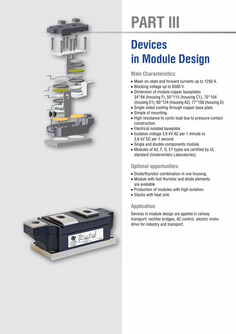
Main Characteristics:• Mean on-state and forward currents up to 1250 А.• Blocking voltage up to 6500 V.• Dimension of module copper baseplates 34*94 (housing F), 50*115 (housing С1), 70*104 (housing Е1), 60*124 (housing А2), 77*150 (housing D).• Single-sided cooling through copper base plate.• Simple of mounting. • High resistance to cyclic load due to pressure contact construction. • Electrical isolated baseplate.• Isolation voltage 3,0 kV АС per 1 minute or 3,6 kV DС per 1 second. • Single and double components module.• Modules of A2, F, D, E1 types are certified by UL standard (Underwriters Laboratories).
Optional opportunities:• Diode/thyristor combination in one housing. • Module with fast thyristor and diode elements are avaliable. • Production of modules with high isolation.• Stacks with heat sink.
Application:Devices in module design are applied in railway transport: rectifier bridges, AC control, electric motor drive for industry and transport.
PART IIIDevices in Module Design

29
Power semiconductor devices
Mod
ule
Desi
gnTh
yris
tors
6500 MTx-240-65-A2
4400 MTx-260-44-A2 MTx-400-44-D
3600 MTx-115-36-F MTx-160-36-C1 МТх-320-З6-А2 MT1-560-36-E MTx-500-36-D
2800 MTx-130-28-F MTx-200-28-C1 MTx-400-28-A2 MT1-635-28-E MTx-630-28-D
2400 MTx-250-24-C1 MTx-430-24-A2
2200 MTx-165-22-F MT1-765-22-E MTx-740-22-D
1800 MTx-201-18-F MTx-320-18-C1 MTx-540-18-A2MT3-595-18-A2 MT1-830-18-E MTx-800-18-D
1200 MTx-650-12-A2 MTx-1000-12-D
800 MTx-1250-8-D
Blocking voltage[V]
baseplatewidth [mm]
34 50 60 70 77
6500 MDx-320-65-A2
5200 MDx-380-52-A2
4400 MDx-470-44-A2 MD1-950-44-E MDx-800-44-D
3600 MDx-155-36-F MDx-250-36-C1 MDx-515-36-A2
3400
2800 MDx-175-28-F MDx-320-28-C1 MD1-1125-28-E MDx-1000-28-D
2600 MDx-580-26-A2
2200 MDx-215-22-F MD1-1280-22-E
1800 MDx-245-18-F MDx-400-18-C1 MDx-660-18-A2
Blocking voltage[V]
baseplatewidth [mm]
34 50 60 70 77
Overview Thyristor Modules for Phase Control
Overview Diode Modules for Rectifier
MT 3 - 540 - 18 - A - N1 2 3 4 5 6
MD 3 - 660 - 18 - A - N1 2 3 4 5 6
Part numbering guide1. Types of module: MT: Thyristor module; MT/D: Thyristor-Diode module; МD/T: Diode-Thyristor module2. Circuit schematic (x): 3-serial connection; 4 - common Cathode; 5-common Anode3. Average on-state current, A4. Voltage code5. Package type 6. Ambient conditions: N - Normal
1. MD- Diode module2. Circuit schematic (x):3 - serial connection; 4 - common Cathode; 5 - common Anode3. Mean forward current, A4. Voltage code5. Package type6. Ambient conditions: N - Normal

30
You can find the Datasheets on our website www.proton-electrotex.com
Part Number
V DRMV RRM
I TSM I TAV V TM I TM
V T(TO)T j max
r T t q T j max R thjc PackageBaseplate
width/length
[V] [kA] [Тс,C0] [V] [A] [V] [mΩ] [μs] [oC] [oC/W] [mm]
up to 1800 VMT1-830-18-E 1000÷1800 33,0 830 (85) 1,45 2500 0,80 0,240 250 130 0,0420 M.E1 70/104
up to 2400 VMT1-765-24-E 2000÷2400 32,0 765 (81) 1,50 2500 0,85 0,277 320 125 0,0420 M.E1 70/104
up to 2800 VMT1-635-28-E 2600÷2800 23,0 635 (85) 1,55 2500 0,95 0,350 320 125 0,0420 M.E1 70/104
up to 3600 VMT1-560-36-E 3000÷3600 21,0 560 (85) 2,10 2500 1,05 0,470 400 125 0,0420 M.E1 70/104
Part Number
V DRMV RRM
I TSM I TAV V TM I TM
V T(TO)T j max
r T t q T j max R thjc PackageBaseplate
width/length
[V] [kA] [Тс,C0] [V] [A] [V] [mΩ] [μs] [oC] [oC/W] [mm]
up to 800 VMTx-1250-8-D
100÷800 34,0 1250 (77) 1,20 3925 0,80 0,120 160 150 0,0500 M.D 77/150MT/Dx-1250-8-DMD/Tx-1250-8-D
up to 1200 VMTx-650-12-A2
1000÷1200 14,0 650 (85) 1,40 1978 0,85 0,280 160 140 0,0650 M.A2 60/124MT/Dx-650-12-A2MD/Tx-650-12-A2MTx-1000-12-D
1000÷1200 32,0 1000 (77) 1,25 3140 0,90 0,150 200 140 0,0500 M.D 77/150MT/Dx-1000-12-DMD/Tx-1000-12-D
up to 1800 VMTx-201-18-F
1000÷1800 6,0 201 (85) 1,40 500 0,80 0,970 125 130 0,1800 M.F1 34/94MT/Dx-201-18-FMD/Tx-201-18-FMTx-320-18-C1
1000÷1800 8,5 320 (86) 1,40 785 0,75 0,500 160 130 0,0600 M.C1 50/115MT/Dx-320-18-C1MD/Tx-320-18-C1MTx-540-18-A2
1400÷1800 15,5 540 (85) 1,50 1570 0,85 0,320 250 130 0,0650 M.A2 60/124MT/Dx-540-18-A2MD/Tx-540-18-A2MT3-595-18-A2
1400÷1800 17,5 595 (85) 1,50 1570 0,84 0,310 320 135 0,0650 M.A2 60/124MT/D3-595-18-A2MD/T3-595-18-A2MTx-800-18-D
1400÷1800 28,0 800 (78) 1,45 2512 0,85 0,230 250 130 0,0500 M.D 77/150MT/Dx-800-18-DMD/Tx-800-18-D
up to 2400 VMTx-165-22-F
2000÷2200 4,7 165 (85) 1,50 500 0,80 1,350 125 125 0,1800 M.F1 34/94MT/Dx-165-22-FMD/Tx-165-22-FMTx-250-24-C1
2000÷2400 7,6 250 (85) 1,50 785 0,80 0,700 200 125 0,0650 M.C1 50/115MT/Dx-250-24-C1MD/Tx-250-24-C1MTx-430-24-A2
2000÷2400 12,0 430 (85) 1,55 1256 1,00 0,410 250 125 0,0650 M.A2 60/124MT/Dx-430-24-A2MD/Tx-430-24-A2MTx-740-24-D
2000÷2400 24,5 740 (77) 1,55 3140 0,90 0,210 320 125 0,0500 M.D 77/150MT/Dx-740-24-DMD/Tx-740-24-D
Single Component Thyristor Modules (МТ1)
Dual Component Thyristor Modules (МТ, MT/D, MD/T)
Devices in Module DesignIII

31
Power semiconductor devices
Mod
ule
Desi
gnTh
yris
tors
Part Number
V DRMV RRM
I TSM I TAV V TM I TM
V T(TO)T j max
r T t q T j max R thjc PackageBaseplate
width/length[mm][V] [kA] [Тс,C
0] [V] [A] [V] [mΩ] [μs] [oC] [oC/W]up to 2800 V
MTx-130-28-F2400÷2800 3,4 130 (85) 1,80 500 0,85 2,400 160 125 0,1900 M.F1 34/94MT/Dx-130-28-F
MD/Tx-130-28-FMTx-200-28-C1
2600÷2800 5,5 200 (87) 2,00 785 0,90 1,100 200 125 0,0650 M.С1 50/115MT/Dx-200-28-C1MD/Tx-200-28-C1MTx-400-28-А2
2600÷2800 9,0 400 (82) 1,80 1256 1,00 0,650 250 125 0,0325 M.А2 60/124MT/Dx-400-28-A2 MD/Tx-400-28-A2 MTx-630-28-D
2600÷2800 21,0 630 (80) 1,40 1978 0,95 0,300 320 125 0,0500 M.D 77/150MT/Dx-630-28-DMD/Tx-630-28-D
up to 3600 VMTx-115-36-F
3000÷3600 2,5 115 (85) 2,45 500 0,95 3,000 200 125 0,1900 M.F1 34/94MT/Dx-115-36-FMD/Tx-115-36-FMTx-160-36-C1
3000÷3600 4,0 160 (81) 2,50 785 1,20 2,300 300 125 0,0650 M.С1 50/115MT/Dx-160-36-C1 MD/Tx-160-36-C1 МТх-320-З6-А2
3000÷3600 5,5 320 (85) 2,20 785 1,15 0,800 320 125 0,0680 M.A2 60/124МТ/Dх-320-З6-А2МD/Тх-320-З6-А2MTx-500-36-D
3000÷3600 18,0 500 (85) 1,85 1570 1,10 0,400 400 125 0,0500 M.D 77/150MT/Dx-500-36-DMD/Tx-500-36-D
up to 4400 VMTx-260-44-A2
3800÷4400 5,0 260 (85) 2,30 628 1,40 1,300 500 125 0,0680 M.A2 60/124MT/Dx-260-44-A2 MD/Tx-260-44-A2MTx-400-44-D
3800÷4400 14,0 400 (88) 2,70 2512 1,20 0,650 500 125 0,0500 M.D 77/150MT/Dx-400-44-D MD/Tx-400-44-D
up to 6500 VMTx-240-65-A2
4600÷6500 4,0 240 (85) 2,80 785 1,10 2,500 630 125 0,0680 M.A2 60/124MT/Dx-240-65-A2 MD/Tx-240-65-A2

32
You can find the Datasheets on our website www.proton-electrotex.com
Part Number
V RRM I FSM I FAV V FM I FM
V F (TO)T j max
r T T j max R thjc PackageBaseplate
width/length[mm][V] [kA] [Тс,C
0] [V] [A] [V] [mΩ] [oC] [oC/W]
up to 2800 VMD1-1125-28-E 2400÷2800 36,0 1125 (100) 1,38 3140 0,80 0,170 160 0,0420 M.E1 70/104
MD1-1280-22-E 2000÷2200 40,0 1280 (100) 1,25 3140 0,80 0,100 160 0,0420 M.E1 70/104
up to 4400 VMD1-950-44-E 3800÷4400 29,0 950 (100) 1,77 2512 0,85 0,280 160 0,0420 M.E1 70/104
Part Number
V RRM I FSM I FAV V FM I FM
V F (TO)T j max
r T T j max R thjc PackageBaseplate
width/length[mm][V] [kA] [Тс,C
0] [V] [A] [V] [mΩ] [oC] [oC/W]
up to 1800 VMDx-245-18-F 1000÷1800 8,1 245 (100) 1,30 500 0,75 0,640 150 0,1800 M.F1 34/94
MDx-400-18-C1 1000÷1800 12,0 400 (102) 1,20 785 0,75 0,250 150 0,0600 M.C1 50/115
MDx-660-18-A2 1000÷1800 19,0 660 (100) 1,40 1978 0,78 0,230 150 0,0650 M.A2 60/124
up to 2800 VMDx-215-22-F 2000÷2200 6,4 215 (100) 1,40 500 0,80 0,920 150 0,1800 M.F1 34/94
MDx-175-28-F 2400÷2800 6,0 175 (100) 1,50 500 0,85 1,500 150 0,1900 M.F1 34/94
MDx-320-28-C1 2000÷2800 8,5 320 (100) 1,40 785 0,85 0,450 150 0,0650 M.C1 50/115
MDx-580-26-A2 2000÷2600 14,0 580 (100) 1,50 1570 0,80 0,350 150 0,0650 M.A2 60/124
MDx-1000-28-D 2000÷2800 32,0 1000 (91) 1,38 3140 0,80 0,150 150 0,0500 M.D 77/150
up to 3600 VMDx-155-36-F 3000÷3600 4,5 155 (100) 2,00 500 0,93 2,000 150 0,1900 M.F1 34/94
MDx-250-36-C1 3000÷3600 5,0 250 (90) 2,00 785 0,90 1,570 150 0,0650 M.C1 50/115
MDx-515-36-A2 3000÷3600 13,0 515 (100) 1,60 1256 0,80 0,500 150 0,0680 M.A2 60/124
up to 4400 VMDx-470-44-A2 3800÷4400 12,0 470 (100) 1,70 1256 0,85 0,600 150 0,0680 M.A2 60/124
MDx-800-44-D 3800÷4400 23,0 800 (85) 1,77 2512 0,90 0,370 150 0,0500 M.D 77/150
up to 6500 VMDx-380-52-A2 4600÷5200 8,0 380 (100) 2,20 1570 0,80 0,800 140 0,0680 M.A2 60/124
MDx-320-65-A2 5400÷6500 6,0 320 (100) 2,40 1570 0,95 1,100 140 0,0680 M.A2 60/124
Single Component Diode Modules (MD1)
Dual Component Diode Modules (MD)
Devices in Module DesignIII

33
Power semiconductor devices
M.A2
M.D
M.C1
M.E1
Package Type
Package Type
Package Type
Package Type
* The screws must be lubricated
* The screws must be lubricated
* The screws must be lubricated
* The screws must be lubricated
Nominal Weight 1500 g
Nominal Weight 3500 g
Nominal Weight 800 g
MT3MT3
MT3
MT/D3MT/D3
MT/D3
MT4MT4
MT4
MD/T3MD/T3
MD/T3
MT5MT5
MT5 MT1
MT/D4MT/D4
MT/D4
MD3MD3
MD3 MD1
MD/T4MD/T4
MD/T4
MD4MD4
MD4
MT/D5MT/D5
MT/D5
MD5MD5
MD5
MD/T5MD/T5
MD/T5
Nominal Weight 2550 g
Mounting Torque (M6) 6.00 Nm (Tolerance ±15%)
Terminal Connection Torque (M10) 12.00 Nm (Tolerance ±15%)
Mounting Torque (M8) 9.00 Nm (Tolerance ±15%)
Terminal Connection Torque (M12) 18.00 Nm (Tolerance ±15%)
Mounting Torque (M6) 6.00 Nm (Tolerance ±15%)
Terminal Connection Torque (M8) 9.00 Nm (Tolerance ±15%)
Mounting Torque (M6) 6.00 Nm (Tolerance ±15%)
Terminal Connection Torque (M12) 18.00 Nm (Tolerance ±15%)
Mod
ule
Desi
gn
34
You can find the Datasheets on our website www.proton-electrotex.com
M.F1Package Type
* The screws must be lubricated
MD3
MT/D3
MT3
MD/T3
MD4 MT4 MD5
MT/D5
Nominal Weight 320 g
Mounting Torque (M6) 6.00 Nm (Tolerance ±15%)
Terminal Connection Torque (M6) 6.00 Nm (Tolerance ±15%)
Wired connection to the module connection wire-assembly №18 (left)A1, A2: MT/T 3, 4, 5; MT/D 3, 4, 5 F1: MT/T 3, 4; MT/D 3, 5C: MT/T 3, 4, 5; MD/T 3, 4, 5 D: MT/T 3, 4, 5; MT/D 3, 4, 5
Wired connection to the module connection wire-assembly №18-01 (right)A2: MT/T 3, 4, 5; MD/T 3, 4, 5 F1: MT/T 3, 4; MD/T 3 E1: MT1C1: MT/T 3, 4, 5; MT/D 3, 4, 5 D: MT/T 3, 4, 5; MD/T 3, 4, 5
Wired connection to the module connection wire-assembly №18-02 (left)A2: MT/T 3, 4, 5; MT/D 3, 4, 5 F1: MT/T 3, 4; MT/D 3, 5C1: MT/T 3, 4, 5; MD/T 3, 4, 5 D: MT/T 3, 4, 5; MT/D 3, 4, 5
Wired connection to the module connection wire-assembly №18-03 (right)A2: MT/T 3, 4, 5; MD/T 3, 4, 5 F1: MT/T 3, 4; MD/T 3 E1: MT1C1: MT/T 3, 4, 5; MT/D 3, 4, 5 D: MT/T 3, 4, 5; MD/T 3, 4, 5
Wired connection of disc devices
Wired connection of disc devices
Avaliable wire connections
III

35
Power semiconductor devices
Type
Weight (without current
lead)
Screw hole diameter (Diameter of the contact
surface)
Overall dimensions without current lead (width/length/height)
Heat resistance (Dissipation capacity)
natural cooling
Heat resistance Air speed is 6 m/sec
Pressure Differential
[kg] [mm] [mm] [°C/W (W)] [°C/W] [Pа]О171 0,669 (0,63) М20х1,5 70х80х100 1,120 (80) 0,355 18О271 1,539 (1,5) М20х1,5 110х110х100 0,710 (130) 0,236 25О371 0,404 (0,365) М20х1,5 45х80х80 1,900 (50) 0,670 15О181 0,672 (0,62) М24х1,5 70х80х100 1,120 (80) 0,355 18О281 1,542 (1,49) М24х1,5 110х110х100 0,710 (130) 0,236 25О123 1,58 (1,45) (22) 126х100х122 0,710 (120) 0,212 20О143 3,18 (2,85) (42) 135х150х125 0,500 (120) 0,125 30О243 5,56 (4,76) (42) 170х150х170 0,280 (220) 0,080 30О343 5,26 (4,46) (42) 170х150х150 0,355 (220) 0,100 30О153 5,57 (4,77) (55) 170х150х176 0,280 (220) 0,075 30О253 5,27 (4,47) (55) 170х150х156 0,355 (220) 0,100 30О173 12,18 (10,57) (82) 200х250х210 0,180 (400) 0,050 40О193 22,9(22,0) 100 300х300х213 0,101 (400) 0,03 29
О 221 - 60 - N1 2 3 4
Part Numbering guide1. О — Heatsink2. Design version3. Length, mm4. Ambient conditions
Heatsinks
Heat
sink
s

Heatsinks
O123O181
O143
O171 O271 O371
O281
O243 O343

37
Power semiconductor devices
Heat
sink
s
O253
O193
O153 O173

Contacts
Country Company Address Telephone/ Fax E-mail/web
Italy
ELCA ACS srl Via Fabio Filzi, 5 +39 0266301574
[email protected] www.elcaacs.it

39
Power semiconductor devices

Proton-Electrotex, JSC19, Leskova Str.,
Orel, 302027, RussiaTel./Fax: +7 4862 440445
Tel.: +7 4862 440642
www.proton-electrotex.com
JULY 2014
Recommended