PHONON ENGINERING &PHONON ENGINERING & CONFINED ACOUSTIC PHONONS IN SILICON MEMBRANESMEMBRANES
Clivia M Sotomayor TorresClivia M Sotomayor Torres
COLLABORATORS
J Cuffe (UCC-IRCSET, IE), E Chavez (CONICYT, Chile), P-O. Chapuis, F Alzina, N Kehagias, L Schneider, T Kehoe, C Ribéreau-Gayon, (ECP, FR) … the ICN team
A Shchepetov M Prunnila S Laakso J AhopeltoA Shchepetov, M Prunnila, S Laakso, J Ahopelto
J Johnson, A A. Maznev J Eliason, A Minnich, K Collins, MIT, , , ,
G Chen, K A Nelson,
A Bruchhausen, M Hettich, O Ristow and T Dekorsy.
El H i (U O jd ) Y P B Dj f i R h iEl-Houssain,(U Oujda), Y Pennec, B Djafari-Rouhani
A Mlayah J Groenen A ZwickA Mlayah, J Groenen, A Zwickand F Poinsotte, U P Sabatier, Toulouse

OUTLINE
• MotivationMotivation• Methods
– Membranes– Inelastic light scatteringe as c g sca e g
• Dispersion relations• Impact on heat transfer• Perspectives and ConclusionsPerspectives and Conclusions
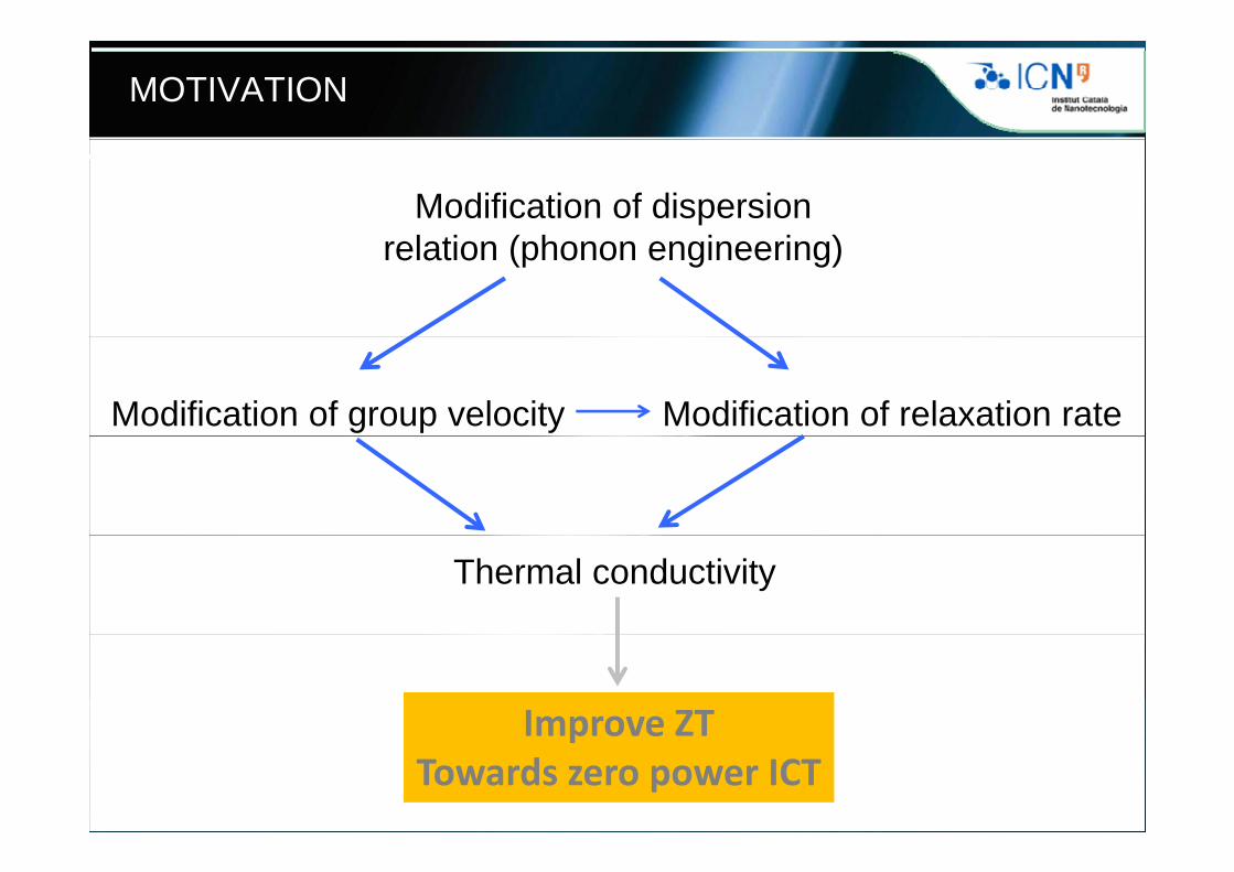
MOTIVATION
Modification of dispersion l ti ( h i i )relation (phonon engineering)
Modification of group velocity Modification of relaxation rate
Thermal conductivity
Improve ZTImprove ZTTowards zero power ICT
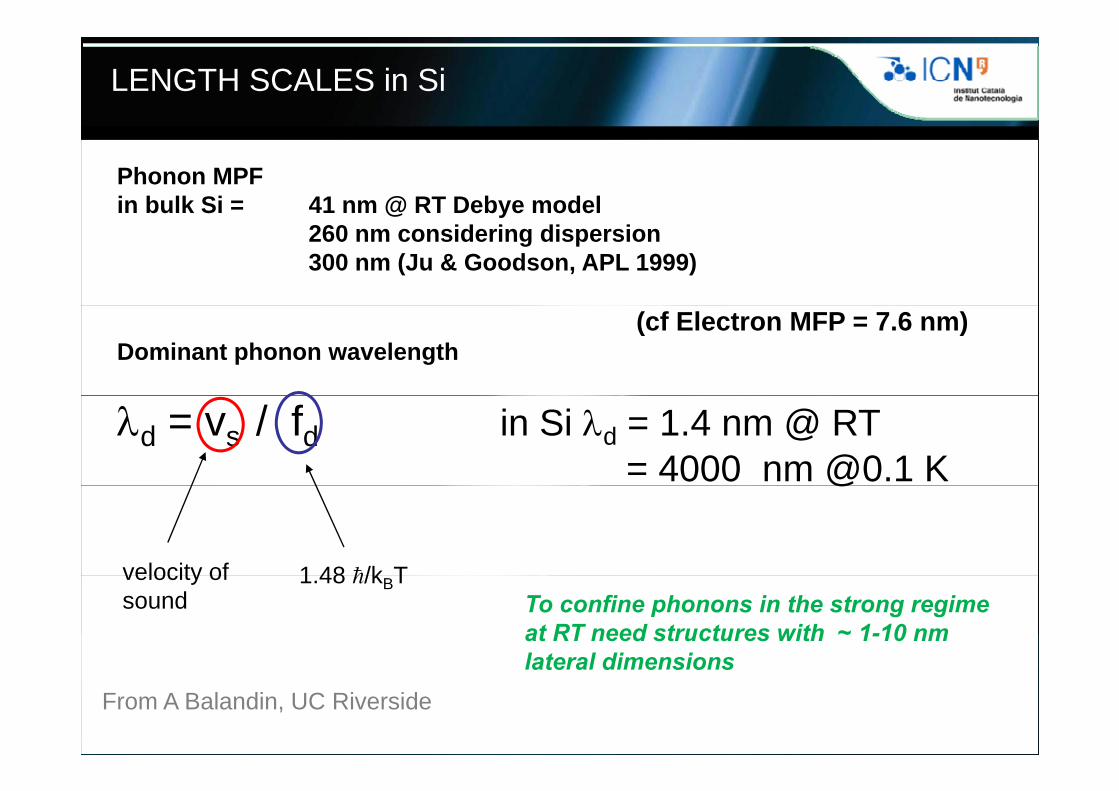
LENGTH SCALES in Si
Phonon MPFin bulk Si = 41 nm @ RT Debye model @ y
260 nm considering dispersion300 nm (Ju & Goodson, APL 1999)
(cf Electron MFP = 7.6 nm)Dominant phonon wavelength
d = vs / fd in Si d = 1.4 nm @ RT= 4000 nm @0.1 K @
velocity of 1 48 /k Tvelocity ofsound
1.48 /kBTTo confine phonons in the strong regime at RT need structures with ~ 1-10 nm lateral dimensions
From A Balandin, UC Riversidelateral dimensions
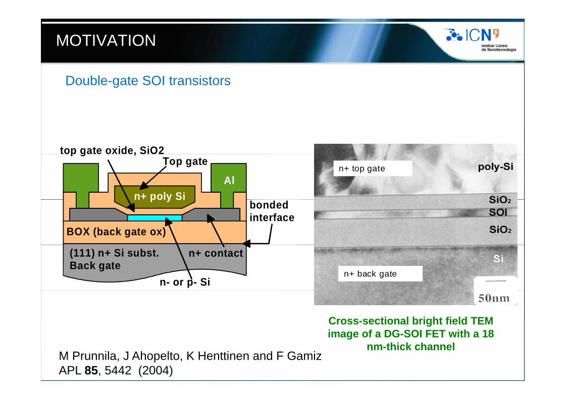
MOTIVATION
Double-gate SOI transistors
top gate oxide, SiO2
Aln+ poly Si
Top gatep g ,
n+ top gate
n poly Si
BOX (back gate ox)
bondedinterface
(111) n+ Si subst.Back gate
n+ contact
n- or p- Sin+ back gate
Cross-sectional bright field TEM image of a DG-SOI FET with a 18image of a DG SOI FET with a 18
nm-thick channelM Prunnila, J Ahopelto, K Henttinen and F GamizAPL 85, 5442 (2004)
MOTIVATION
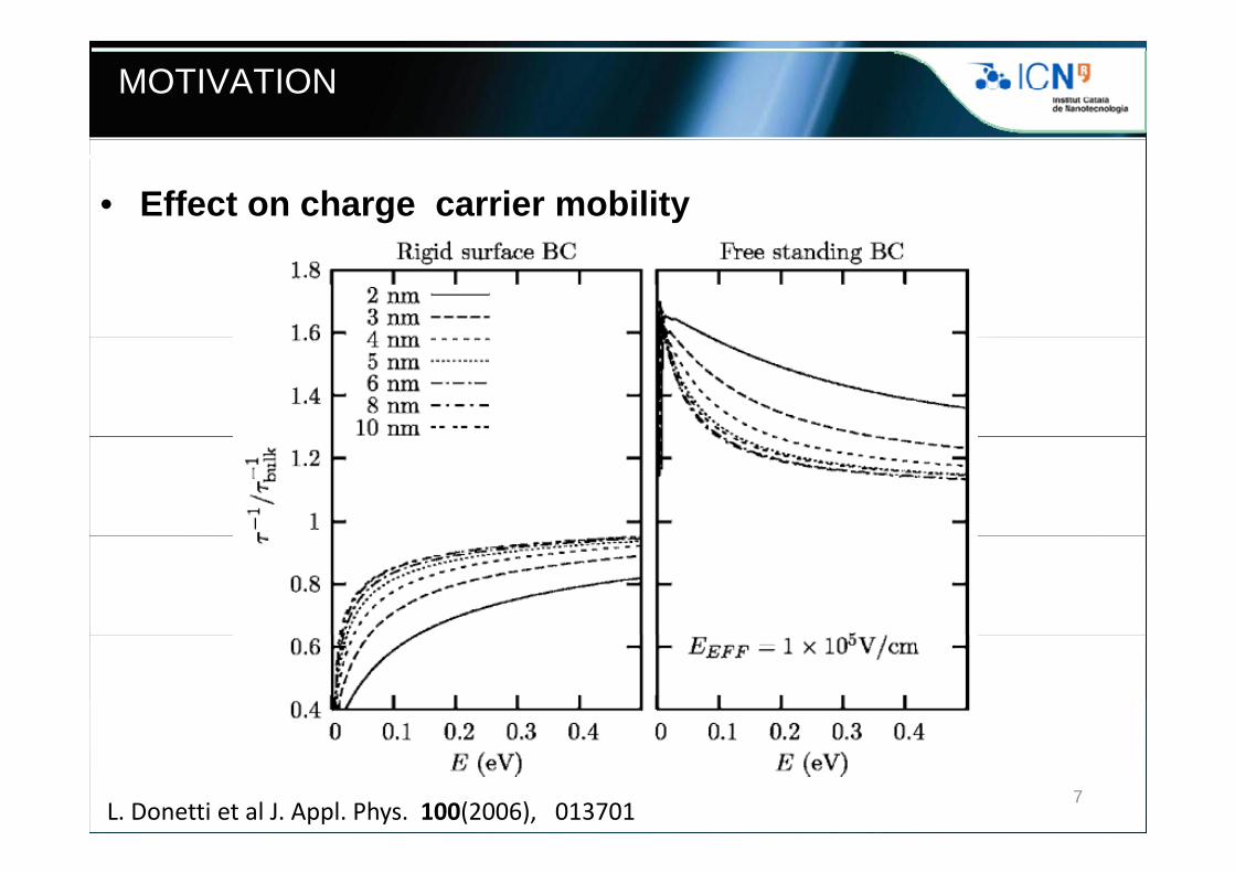
• Effect on charge carrier mobility
7L. Donetti et al J. Appl. Phys. 100(2006), 013701
MOTIVATION
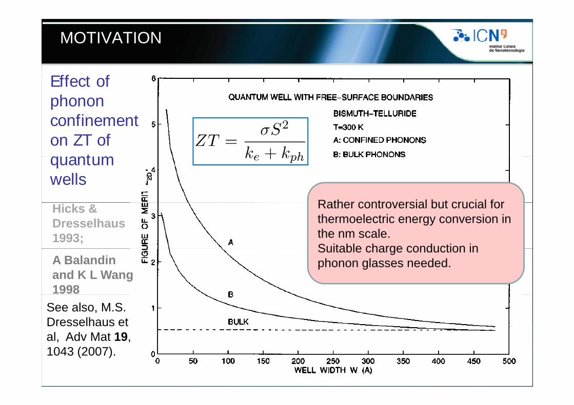
Effect of phonon confinement on ZT of quantumquantum wells
Rather controversial but crucial forHicks & Dresselhaus1993;
Rather controversial but crucial for thermoelectric energy conversion in the nm scale.Suitable charge conduction in
A Balandin and K L Wang 1998
Suitable charge conduction in phonon glasses needed.
See also, M.S. Dresselhaus et al, Adv Mat 19,al, Adv Mat 19, 1043 (2007).
MOTIVATION
Phononic crystals– Acoustic and elastic analogues of photonic crystals– ‘stop bands’ in phonon spectrum (phonon mirrors); – ‘negative refraction’ of phonons (phonon caustics)– Good theory available: Multiple scattering theory for
elastic and acoustic waves. See, for example:Kafesaki & Economou PRB 60, 11993 (1999), Liu et al PRB 62 2446 (2000)Liu et al PRB 62, 2446 (2000)Psaroba et al PRB 62, 278 (2000).
And for a database 2006-2008:http://www.phys.uoa.gr/phononics/PhononicDatabase.ht
ml… cell phones have phononic crystal-like BAW filters
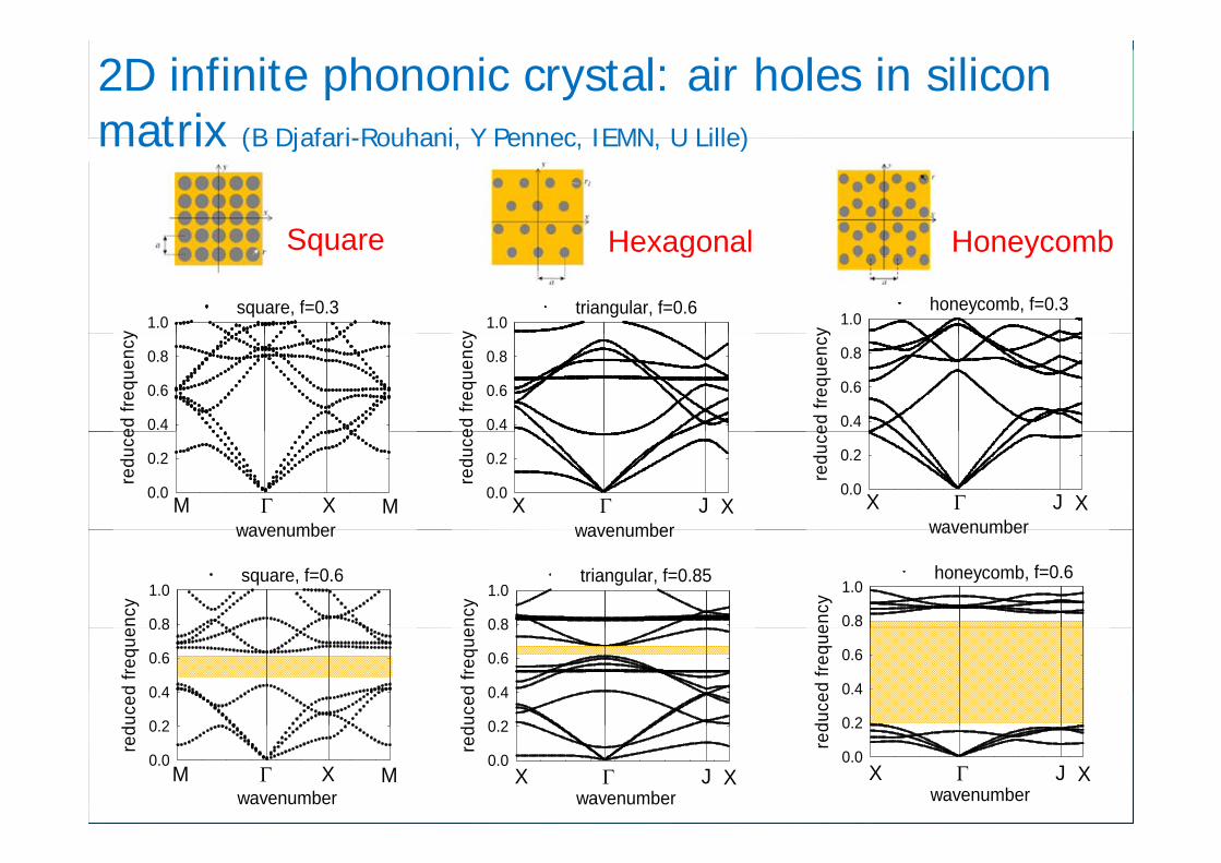
2D infinite phononic crystal: air holes in siliconmatrix (B Djafari-Rouhani Y Pennec IEMN U Lille)matrix (B Djafari-Rouhani, Y Pennec, IEMN, U Lille)
Square He agonal Hone comb
y 1.0triangular, f=0.6
y 1.0square, f=0.3
y 1.0honeycomb, f=0.3
Square Hexagonal Honeycomb
ed fr
eque
ncy
0.4
0.6
0.8
ed fr
eque
ncy
0.4
0.6
0.8
ed fr
eque
ncy
0.4
0.6
0.8
wavenumber
redu
ce0.0
0.2
X J Xwavenumber
redu
ce
0.0
0.2
M X Mwavenumber
redu
ce
0.0
0.2
X J Xwavenumber
ncy
0 8
1.0triangular, f=0.85
wavenumber
ncy
0 8
1.0square, f=0.6
wavenumber
ency
0.8
1.0honeycomb, f=0.6
uced
freq
ue
0 2
0.4
0.6
0.8
uced
freq
ue
0 2
0.4
0.6
0.8
duce
d fre
que
0 2
0.4
0.6
wavenumber
red
0.0
0.2
X J Xwavenumber
red
0.0
0.2
M X Mwavenumber
red
0.0
0.2
X J X
MOTIVATION
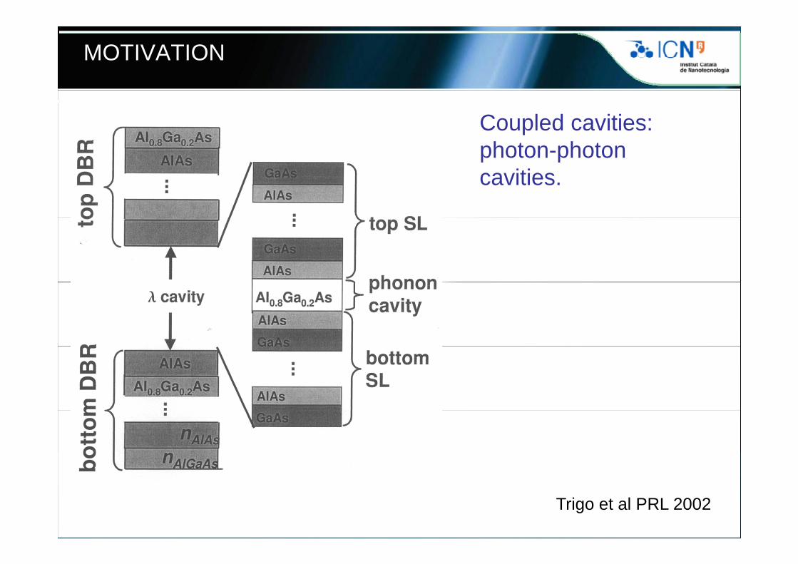
Coupled cavities: photon-photonphoton photon cavities.
Trigo et al PRL 2002
MOTIVATION
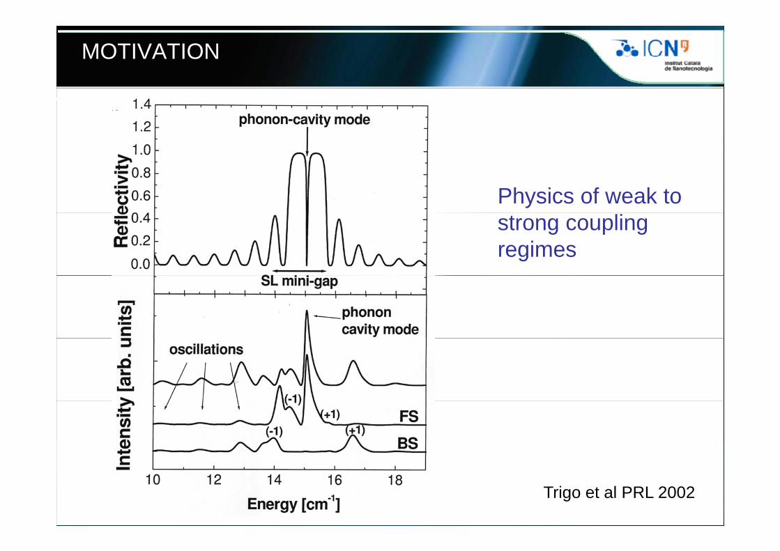
Physics of weak to strong coupling regimes
Trigo et al PRL 2002
MOTIVATION
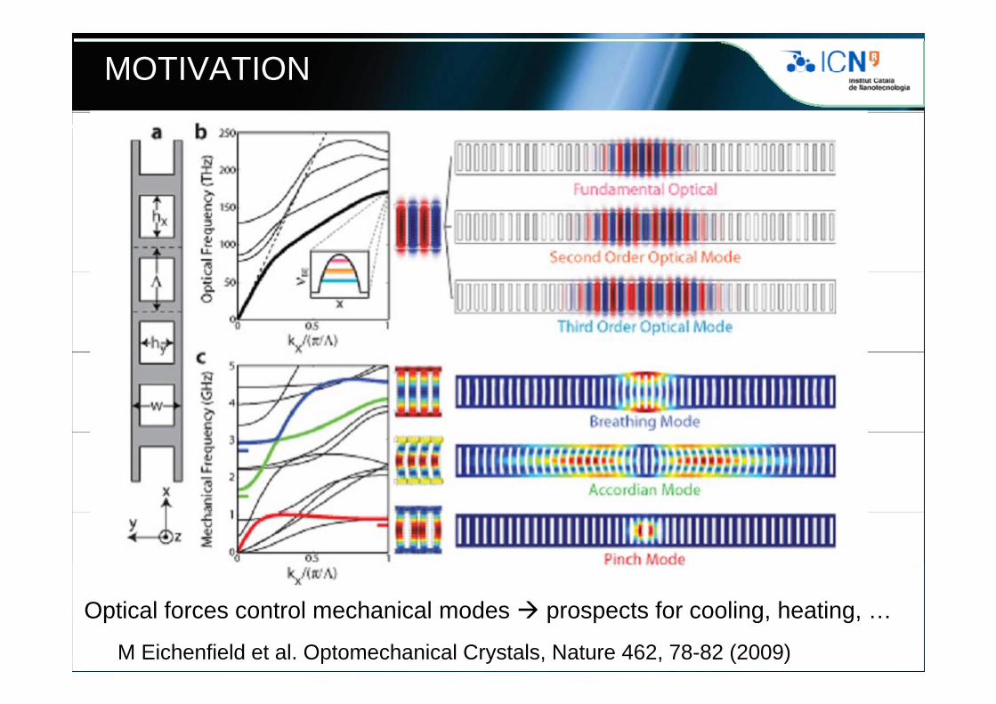
M Eichenfield et al. Optomechanical Crystals, Nature 462, 78-82 (2009)
Optical forces control mechanical modes prospects for cooling, heating, …
MOTIVATION
Acoustic phonons have also an impact in:
Noise and thermal limits in NEMS and nanoelectronics Coherence control in quantum information processing Phonon engineering: sources, detectors and other
components Photon-phonon coupling: Phoxonic Crystals and Opto
mechanical oscillators Energy harvesting and storage THz technologies for medical diagnostic and securityg g y Elastic material parameters down to the nm-scale
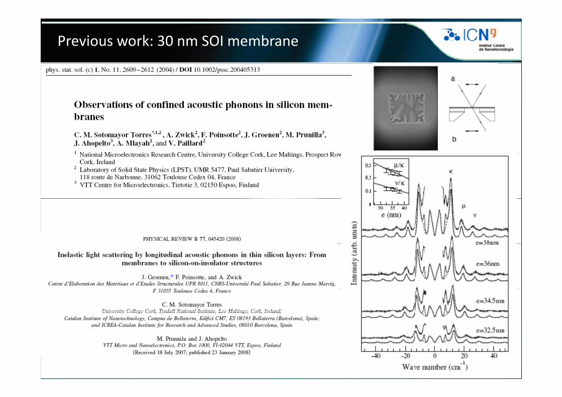
Previous work: 30 nm SOI membrane
HYPOTHESIS and STATEMENT
The confinement of phonons modifies their frequencies and density of states affectingfrequencies and density of states affecting group velocities of modes, scattering mechanisms lifetimes and changesmechanisms, lifetimes and changes assumptions about boundary conditions and transport propertiestransport properties.
Understanding of acoustic phonons confinement in nanostructures is crucial for phonon engineering and strategies for low power nanoelectronics.
OUTLINE
• MotivationMotivation• Methods
– Membranes– Inelastic light scatteringe as c g sca e g
• Dispersion relations• Impact on heat transfer• Perspectives and ConclusionsPerspectives and Conclusions
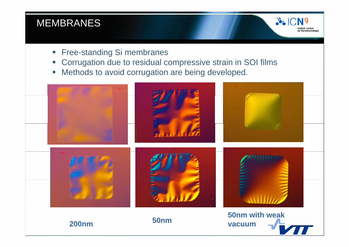
MEMBRANES
Free-standing Si membranes Corrugation due to residual compressive strain in SOI films Methods to avoid corrugation are being developed.
200nm 50nm50nm with weak vacuum
MEMBRANES
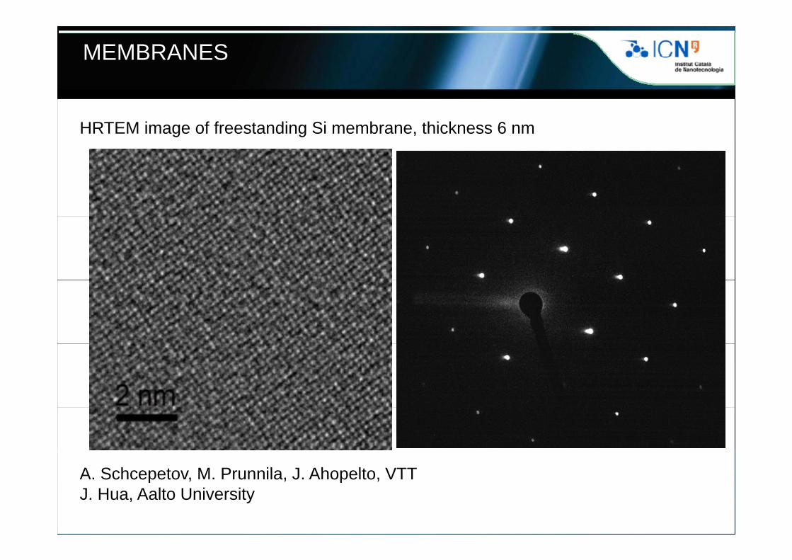
HRTEM image of freestanding Si membrane, thickness 6 nm
A Schcepetov M Prunnila J Ahopelto VTTA. Schcepetov, M. Prunnila, J. Ahopelto, VTTJ. Hua, Aalto University

OUTLINE
• MotivationMotivation• Methods
– Membranes– Inelastic light scatteringe as c g sca e g
• Dispersion relations• Impact on heat transfer• Perspectives and ConclusionsPerspectives and Conclusions
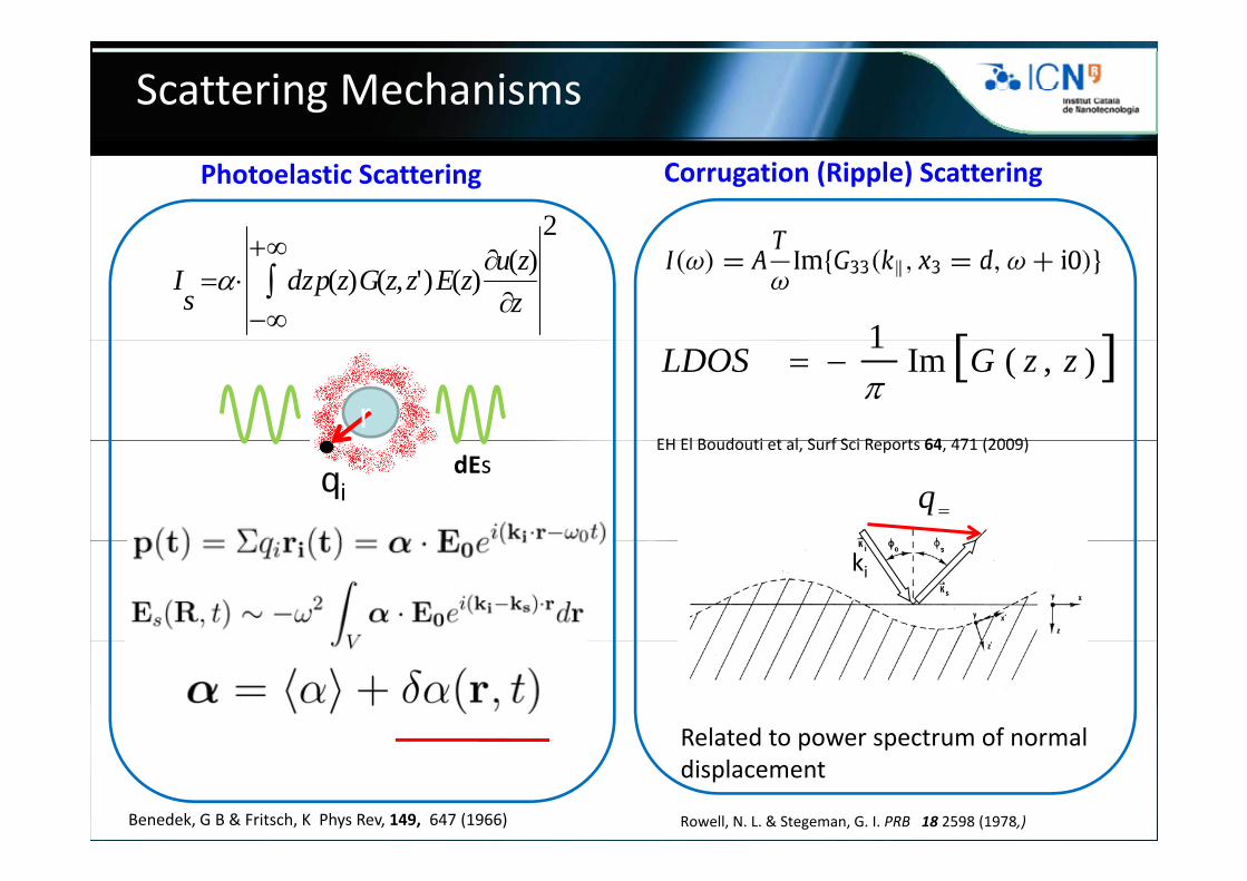
Scattering Mechanisms
Photoelastic Scattering Corrugation (Ripple) Scattering
2)(
)( )',( )(
zzu
zEzzGzpdzs
I
1
rEH El B d ti t l S f S i R t 64 471 (2009)
),(Im 1
zzGLDOS
qii dEs
EH El Boudouti et al, Surf Sci Reports 64, 471 (2009)
q
kski
Related to power spectrum of normal
Benedek, G B & Fritsch, K Phys Rev, 149, 647 (1966) Rowell, N. L. & Stegeman, G. I. PRB 18 2598 (1978,)
Related to power spectrum of normal displacement
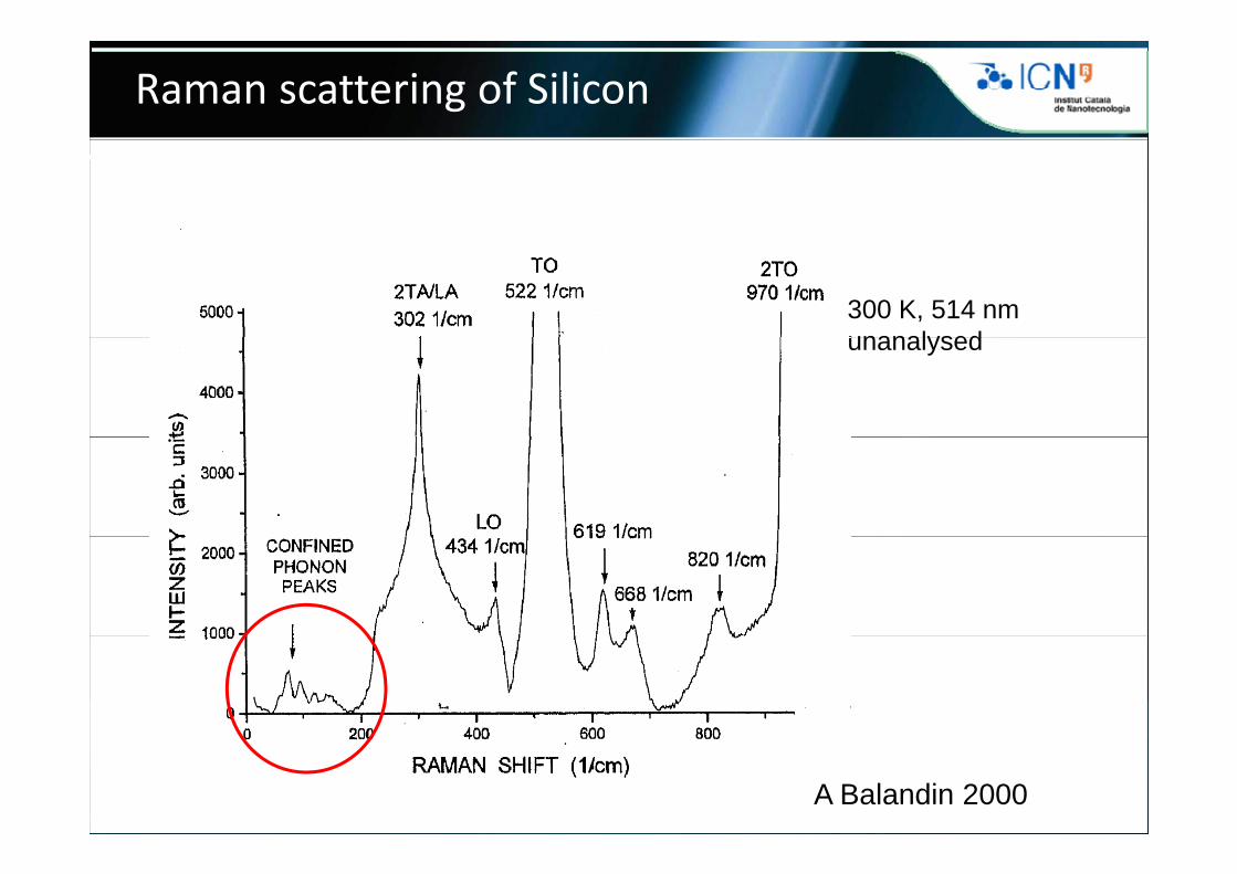
Raman scattering of Silicon
300 K, 514 nm unanalysedunanalysed
A Balandin 2000
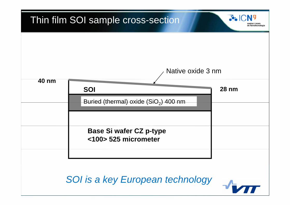
Thin film SOI sample cross-section
Native oxide 3 nm40
Buried (thermal) oxide (SiO2) 400 nm
SOI 40 nm
28 nm
Buried (thermal) oxide (SiO2) 400 nm
Base Si wafer CZ p-type <100> 525 micrometer
SOI is a key European technology
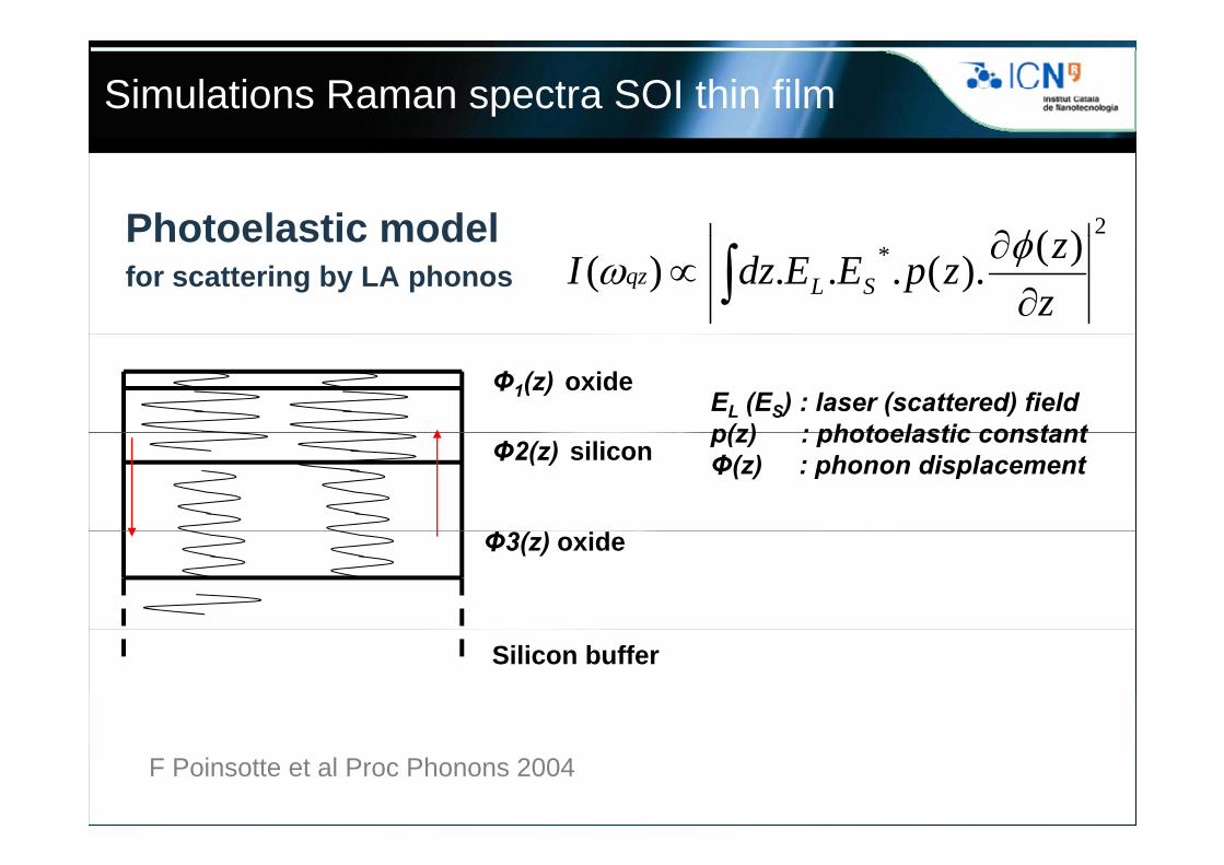
Simulations Raman spectra SOI thin film
Photoelastic model 2)(Photoelastic model for scattering by LA phonos
* )().(...)(
zzzpEEdzI SLqz
EL (ES) : laser (scattered) fieldp(z) : photoelastic constant
Φ1(z) oxide
p(z) : photoelastic constantΦ(z) : phonon displacementΦ2(z) silicon
Φ3(z) oxide
Silicon buffer
F Poinsotte et al Proc Phonons 2004
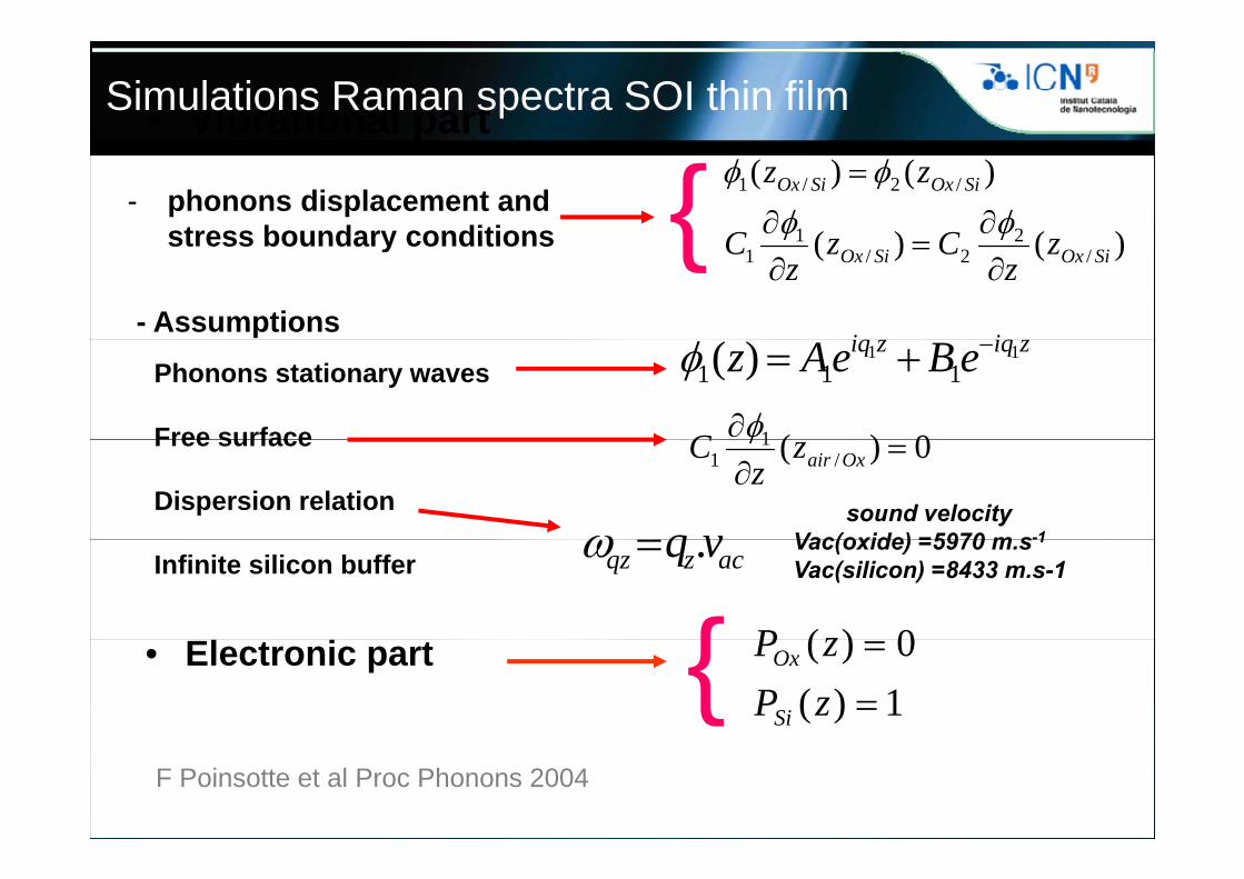
• Vibrational partSimulations Raman spectra SOI thin film
- phonons displacement and stress boundary conditions )()(
)()(
21
/2/1 SiOxSiOx
zCzC
zz
p
{stress boundary conditions )()( /2
2/1
1 SiOxSiOx zz
Czz
C
ii- Assumptions
{Phonons stationary waves
Free surface
ziqziq eBeAz 11111 )(
0)(1C Free surface
Dispersion relation
0)( /1
1 Oxairzz
C
vqsound velocity
Vac(oxide) =5970 m s-1
Infinite silicon buffer
0)(zP
aczqz vq . Vac(oxide) =5970 m.s-1
Vac(silicon) =8433 m.s-1
{• Electronic part1)(0)(
zPzP
Si
Ox{F Poinsotte et al Proc Phonons 2004
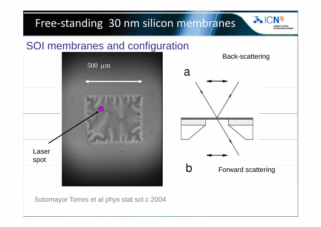
Free‐standing 30 nm silicon membranes
SOI membranes and configurationBack-scattering
500 m
Laser spot
Forward scattering
Sotomayor Torres et al phys stat sol c 2004
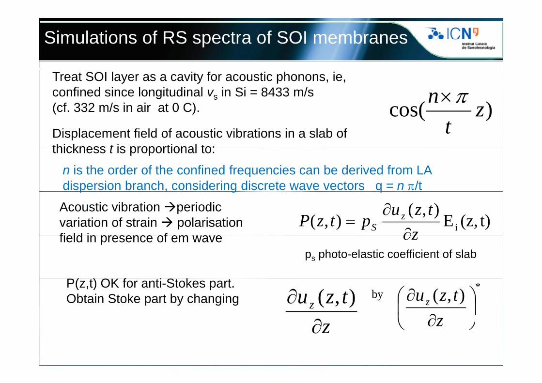
Simulations of RS spectra of SOI membranes
)(n Treat SOI layer as a cavity for acoustic phonons, ie, confined since longitudinal vs in Si = 8433 m/s ( f 332 / i i t 0 C) )cos( z
t(cf. 332 m/s in air at 0 C).
Displacement field of acoustic vibrations in a slab of thickness t is proportional to:
n is the order of the confined frequencies can be derived from LA dispersion branch, considering discrete wave vectors q = n /t
thickness t is proportional to:
p , g qAcoustic vibration periodicvariation of strain polarisationfi ld i f
t)(z,E),(
),( iztzu
ptzP zS
field in presence of em wave z
ps photo-elastic coefficient of slab
P( ) OK f i S ktzuz
),( *),(
ztzuz
P(z,t) OK for anti-Stokes part.Obtain Stoke part by changing by
z z
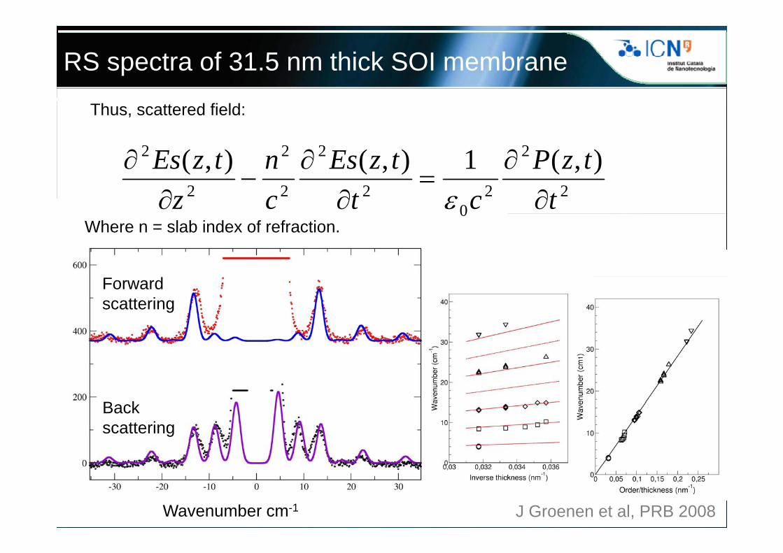
RS spectra of 31.5 nm thick SOI membrane
2222 )(1)()( PEE
Thus, scattered field:
2
2
20
2
2
2
2
2
2 ),(1),(),(t
tzPct
tzEscn
ztzEs
0Where n = slab index of refraction.
Forward scattering
B kBack scattering
Wavenumber cm-1 J Groenen et al, PRB 2008
OUTLINE
• MotivationMotivation• Methods
– Membranes– Inelastic light scatteringe as c g sca e g
• Dispersion relations (mainly by J Cuffe, E Chavez, both PhD students at ICN work unpublished)both PhD students at ICN, work unpublished)
• Impact on heat transfer• Perspectives and Conclusions
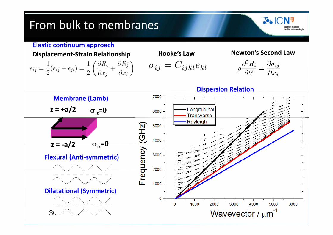
From bulk to membranes
Newton’s Second LawDisplacement‐Strain RelationshipElastic continuum approach
Hooke’s Law
Dispersion RelationMembrane (Lamb)
iz=0z = +a/2
Dispersion Relation
z = a/2 =0
Flexural (Anti‐symmetric)
z = ‐a/2 iz=0
Dilatational (Symmetric)
30
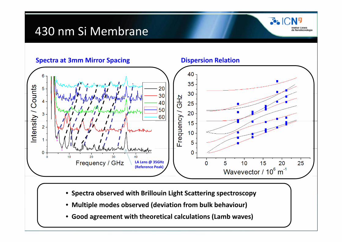
430 nm Si Membrane
Spectra at 3mm Mirror Spacing Dispersion Relation
LA Lens @ 35GHz(Reference Peak)
• Spectra observed with Brillouin Light Scattering spectroscopy
M lti l d b d (d i ti f b lk b h i )• Multiple modes observed (deviation from bulk behaviour)
• Good agreement with theoretical calculations (Lamb waves)
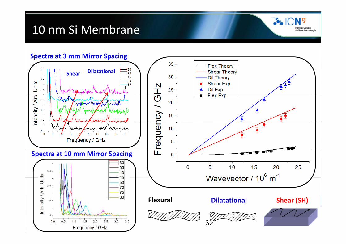
10 nm Si Membrane
Spectra at 3 mm Mirror Spacing
DilatationalShear
Spectra at 10 mm Mirror Spacing
Flexural Dilatational Shear (SH)
32
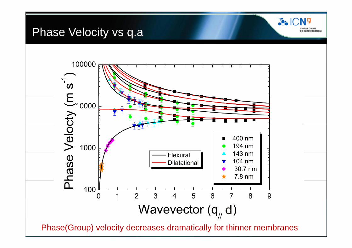
Phase Velocity vs q.a
Phase(Group) velocity decreases dramatically for thinner membranes
OUTLINE
• MotivationMotivation• Methods
– Membranes– Inelastic light scatteringe as c g sca e g
• Dispersion relations• Impact on heat transfer• Perspectives and ConclusionsPerspectives and Conclusions
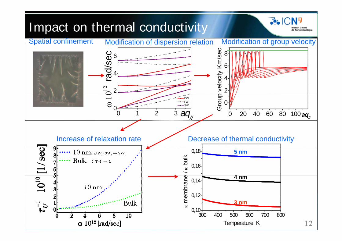
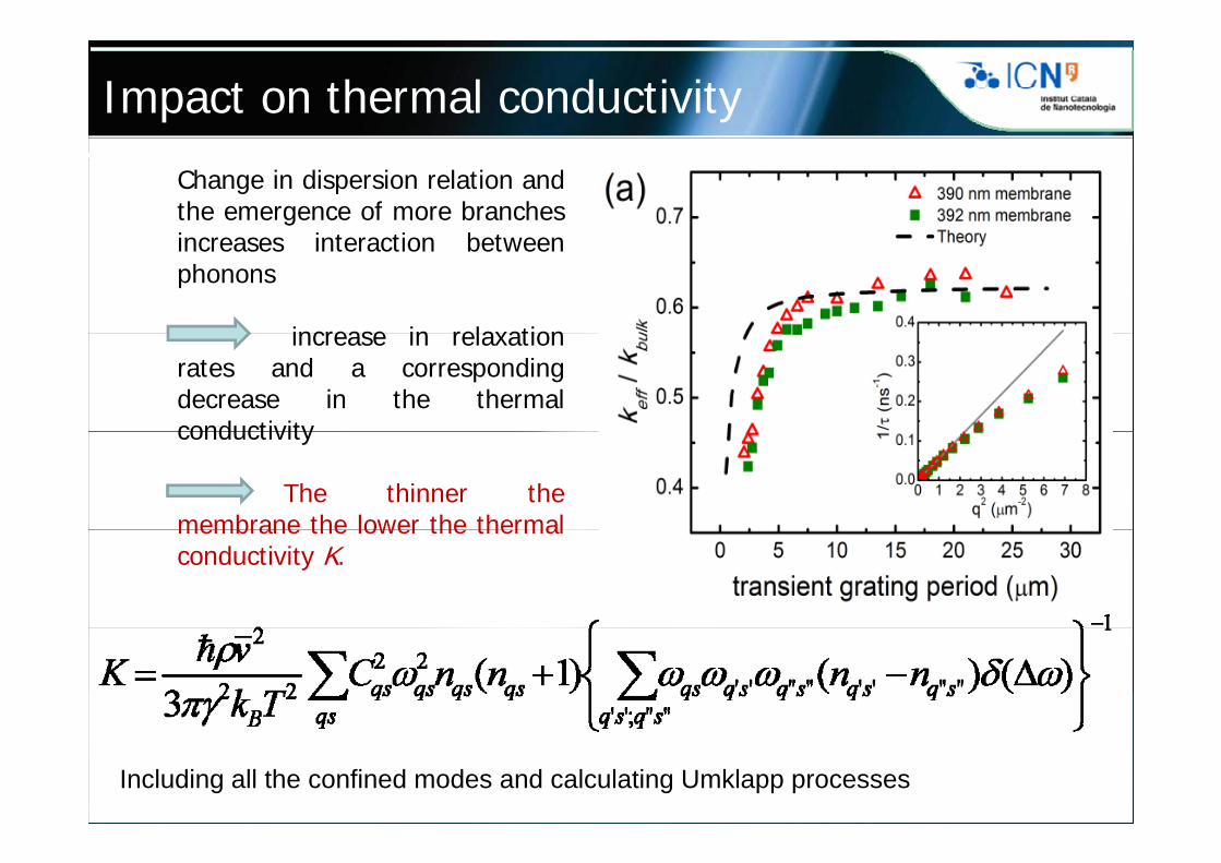
S i l fiImpact on thermal conductivity
6
8
Km
/sec6
/sec
Spatial confinement Modification of dispersion relation Modification of group velocity
2
4
6
velo
city
K
2
4
rad/
0 20 40 60 80 100
0
Gro
up
aq//0 1 2 3
0
DW FW SW
aq//
Increase of relaxation rate Decrease of thermal conductivity
0,16
0,18
e /
bul
k 5 nm
4
0,12
0,14
mem
bran
e 4 nm
3 nm
300 400 500 600 700 8000,10
m
Temperature K
3 nm
Impact on thermal conductivity
Change in dispersion relation andthe emergence of more branchesi i t ti b tincreases interaction betweenphonons
increase in relaxationincrease in relaxationrates and a correspondingdecrease in the thermalconductivityconductivity
The thinner themembrane the lower the thermalmembrane the lower the thermalconductivity K.
Including all the confined modes and calculating Umklapp processes
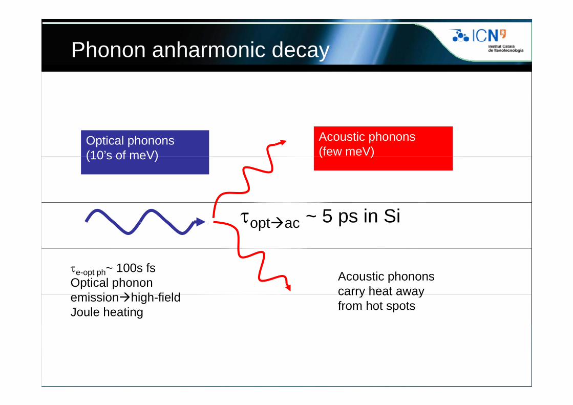
Phonon anharmonic decay
Optical phonons(10’s of meV)
Acoustic phonons(few meV)(10 s of meV) ( )
optac ~ 5 ps in Si
e-opt ph~ 100s fsOptical phonon
i i hi h fi ld
Acoustic phonons carry heat awayemissionhigh-field
Joule heating
carry heat away from hot spots
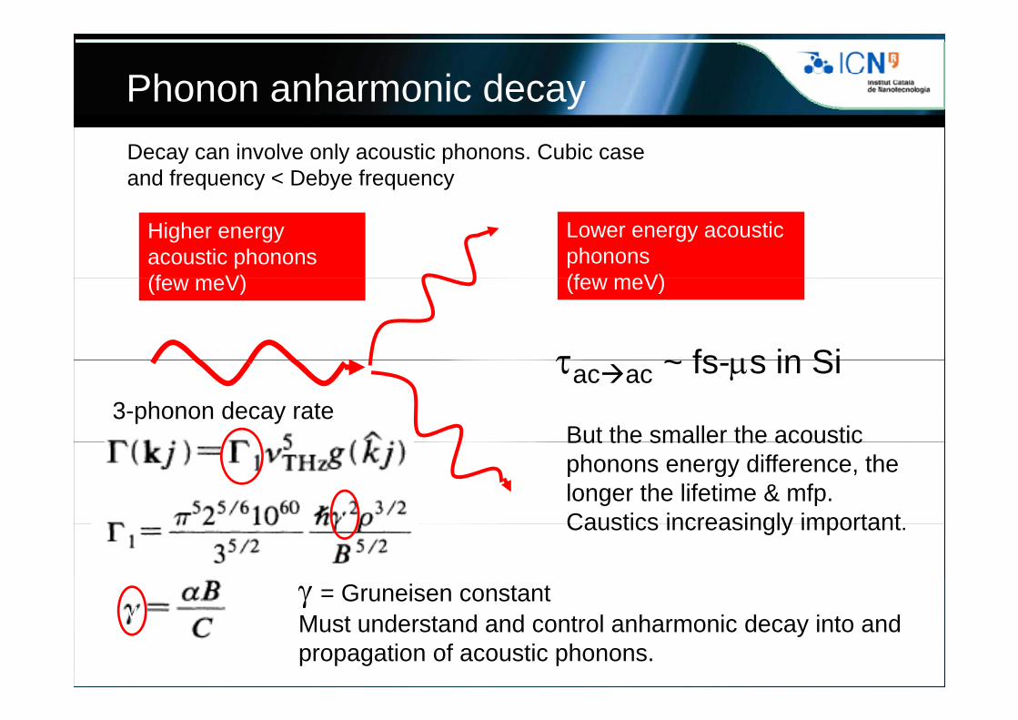
Phonon anharmonic decayDecay can involve only acoustic phonons. Cubic case and frequency < Debye frequency
Lower energy acoustic phonons(few meV)
Higher energy acoustic phonons(f V) (few meV)
~ fs s in Si
(few meV)
acac ~ fs-s in Si
But the smaller the acoustic3-phonon decay rate
But the smaller the acoustic phonons energy difference, the longer the lifetime & mfp.Caustics increasingly importantv
v
Caustics increasingly important.
= Gruneisen constantMust understand and control anharmonic decay into and propagation of acoustic phonons.
v
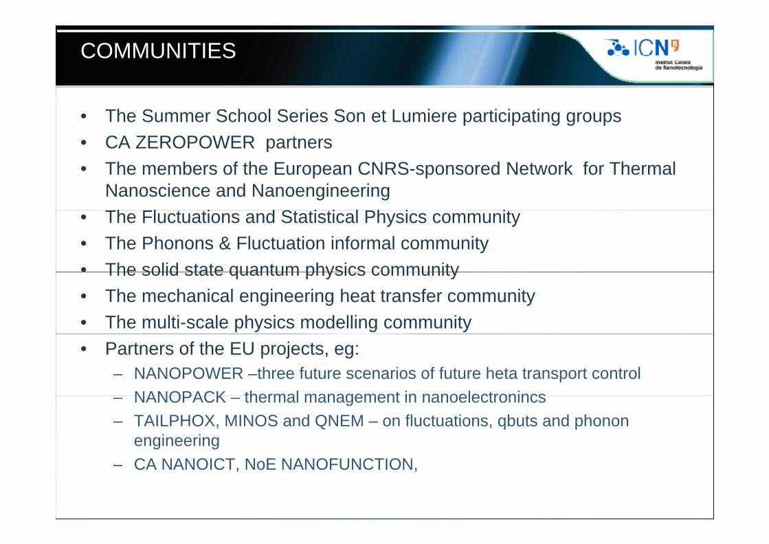
COMMUNITIES
• The Summer School Series Son et Lumiere participating groups• CA ZEROPOWER partnersp• The members of the European CNRS-sponsored Network for Thermal
Nanoscience and NanoengineeringTh Fl t ti d St ti ti l Ph i it• The Fluctuations and Statistical Physics community
• The Phonons & Fluctuation informal community• The solid state quantum physics communityThe solid state quantum physics community• The mechanical engineering heat transfer community• The multi-scale physics modelling community • Partners of the EU projects, eg:
– NANOPOWER –three future scenarios of future heta transport controlNANOPACK thermal management in nanoelectronincs– NANOPACK – thermal management in nanoelectronincs
– TAILPHOX, MINOS and QNEM – on fluctuations, qbuts and phonon engineering
– CA NANOICT, NoE NANOFUNCTION,

OUTLINE
• MotivationMotivation• Methods
– Membranes– Inelastic light scatteringe as c g sca e g
• Dispersion relations• Impact on heat transfer• Perspectives and ConclusionsPerspectives and Conclusions
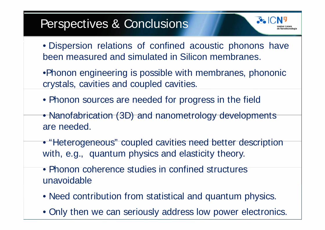
Perspectives & Conclusions
• Dispersion relations of confined acoustic phonons havebeen measured and simulated in Silicon membranes.
•Phonon engineering is possible with membranes, phononiccrystals, cavities and coupled cavities.
• Phonon sources are needed for progress in the field
• Nanofabrication (3D) and nanometrology developments• Nanofabrication (3D) and nanometrology developments are needed.
• “Heterogeneous” coupled cavities need better description• Heterogeneous coupled cavities need better description with, e.g., quantum physics and elasticity theory.
Phonon cohe ence st dies in confined st ct es• Phonon coherence studies in confined structures unavoidable
N d t ib ti f t ti ti l d t h i• Need contribution from statistical and quantum physics.
• Only then we can seriously address low power electronics.
Support
Large InstallationIMB CNMIMB‐CNM, GICSERV 2010 grant
43
2010 grant
Recommended