1 Nic
olo
Ca
rtig
lia, I
NFN
, To
rino
– T
RED
I 201
6
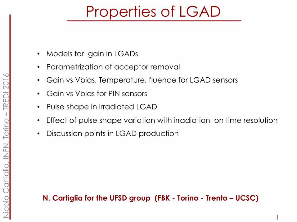
Properties of LGAD
• Models for gain in LGADs
• Parametrization of acceptor removal
• Gain vs Vbias, Temperature, fluence for LGAD sensors
• Gain vs Vbias for PIN sensors
• Pulse shape in irradiated LGAD
• Effect of pulse shape variation with irradiation on time resolution
• Discussion points in LGAD production
N. Cartiglia for the UFSD group (FBK - Torino - Trento – UCSC)
2 Nic
olo
Ca
rtig
lia, I
NFN
, To
rino
– T
RED
I 201
6
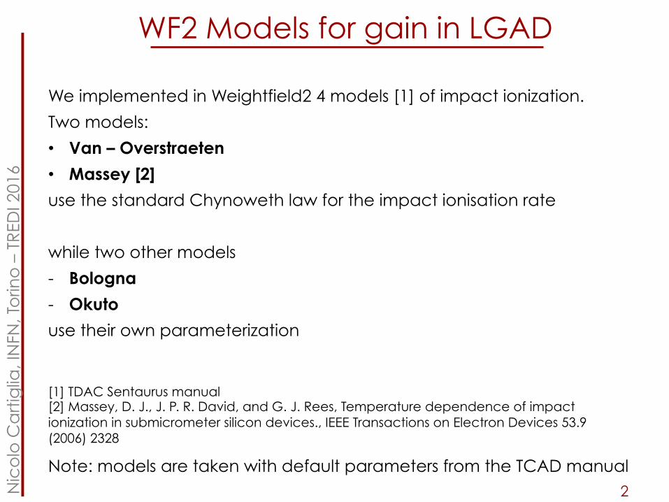
WF2 Models for gain in LGAD
We implemented in Weightfield2 4 models [1] of impact ionization.
Two models:
• Van – Overstraeten
• Massey [2]
use the standard Chynoweth law for the impact ionisation rate
while two other models
- Bologna
- Okuto
use their own parameterization
Note: models are taken with default parameters from the TCAD manual
[1] TDAC Sentaurus manual [2] Massey, D. J., J. P. R. David, and G. J. Rees, Temperature dependence of impact ionization in submicrometer silicon devices., IEEE Transactions on Electron Devices 53.9 (2006) 2328
3 Nic
olo
Ca
rtig
lia, I
NFN
, To
rino
– T
RED
I 201
6
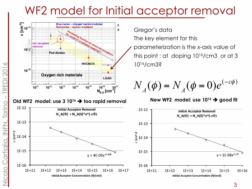
WF2 model for Initial acceptor removal
Gregor’s data
The key element for this
parameterization is the x-axis value of
this point : at doping 1016/cm3 or at 3
1016/cm3?
Old WF2 model: use 3 1016 è too rapid removal New WF2 model: use 1016 è good fit
NA(φ) = NA(φ = 0)e(−cφ )
4 Nic
olo
Ca
rtig
lia, I
NFN
, To
rino
– T
RED
I 201
6
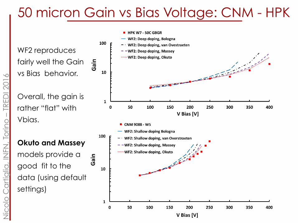
50 micron Gain vs Bias Voltage: CNM - HPK
WF2 reproduces
fairly well the Gain
vs Bias behavior.
Overall, the gain is
rather “flat” with
Vbias.
Okuto and Massey
models provide a
good fit to the
data (using default
settings)
5 Nic
olo
Ca
rtig
lia, I
NFN
, To
rino
– T
RED
I 201
6
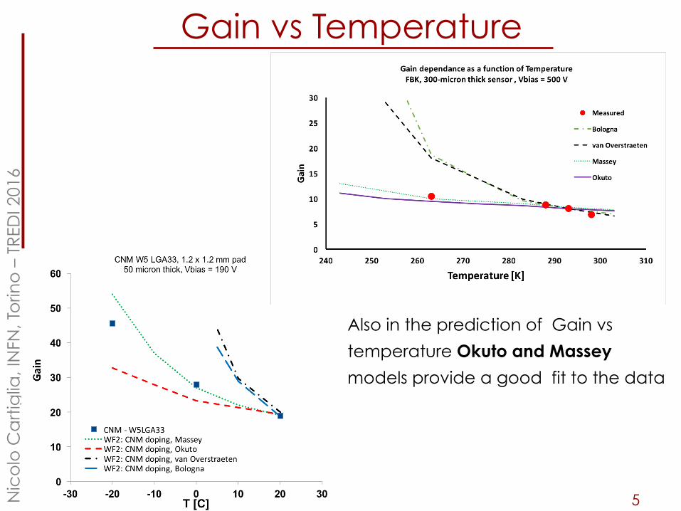
Gain vs Temperature
Also in the prediction of Gain vs
temperature Okuto and Massey
models provide a good fit to the data
6 Nic
olo
Ca
rtig
lia, I
NFN
, To
rino
– T
RED
I 201
6
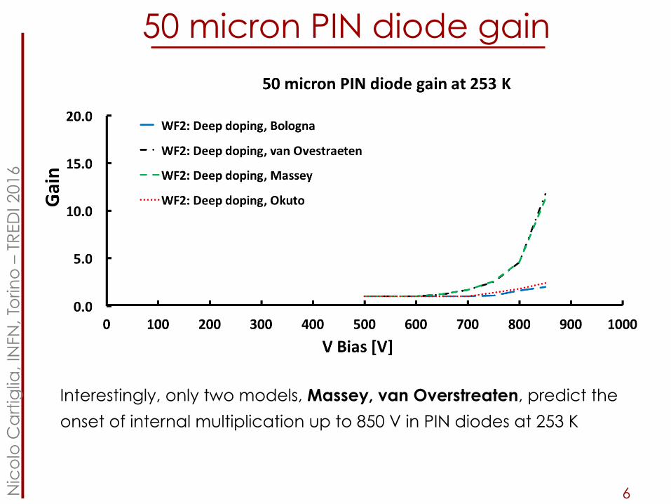
50 micron PIN diode gain
Interestingly, only two models, Massey, van Overstreaten, predict the
onset of internal multiplication up to 850 V in PIN diodes at 253 K

7 Nic
olo
Ca
rtig
lia, I
NFN
, To
rino
– T
RED
I 201
6
Gain vs Irradiation - neutron This plot contains a massive amount of information (CNM R9088).
Can we have a model for this?
Can we explain the evolution of Vbias @ gain = 10 as a function of
radiation?
G = 10
CNM sensor R9088
8 Nic
olo
Ca
rtig
lia, I
NFN
, To
rino
– T
RED
I 201
6
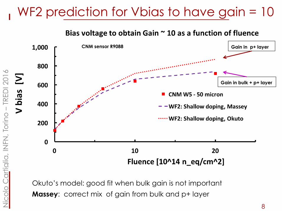
WF2 prediction for Vbias to have gain = 10
Okuto’s model: good fit when bulk gain is not important
Massey: correct mix of gain from bulk and p+ layer
Gain in bulk + p+ layer
Gain in p+ layer CNM sensor R9088
9 Nic
olo
Ca
rtig
lia, I
NFN
, To
rino
– T
RED
I 201
6
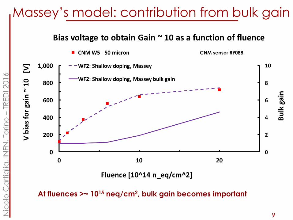
Massey’s model: contribution from bulk gain
At fluences >~ 1015 neq/cm2, bulk gain becomes important
CNM sensor R9088
10 Nic
olo
Ca
rtig
lia, I
NFN
, To
rino
– T
RED
I 201
6
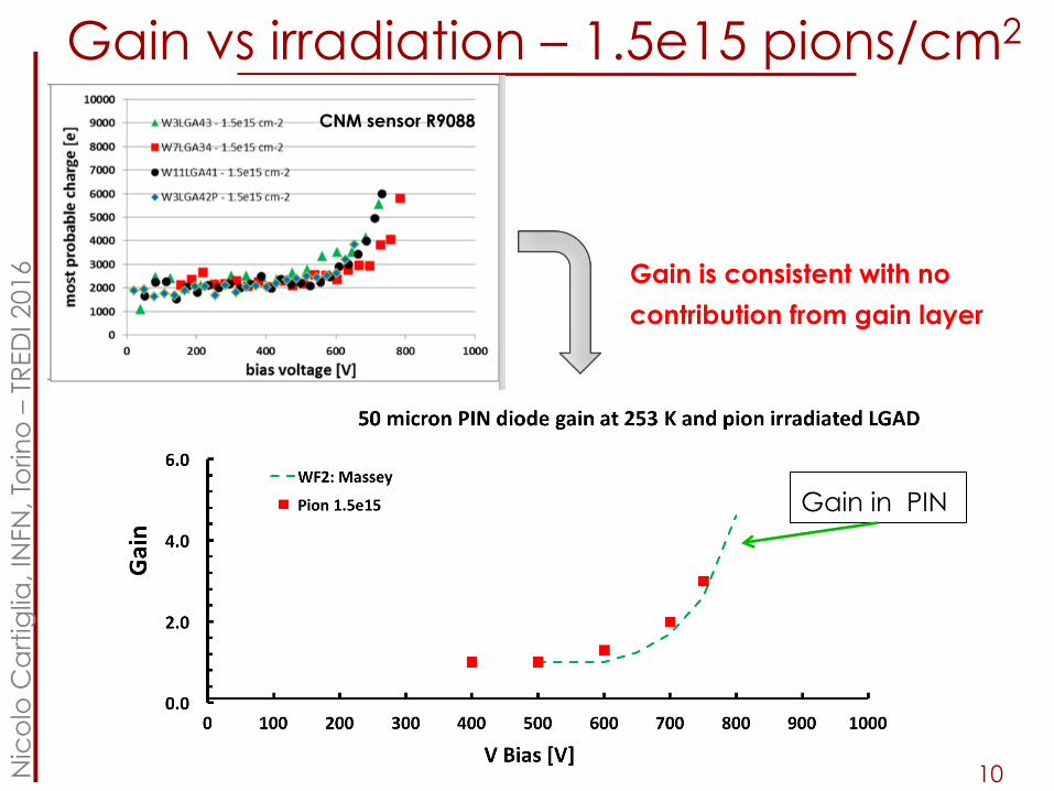
Gain vs irradiation – 1.5e15 pions/cm2
Gain is consistent with no
contribution from gain layer
Gain in PIN
CNM sensor R9088
11 Nic
olo
Ca
rtig
lia, I
NFN
, To
rino
– T
RED
I 201
6
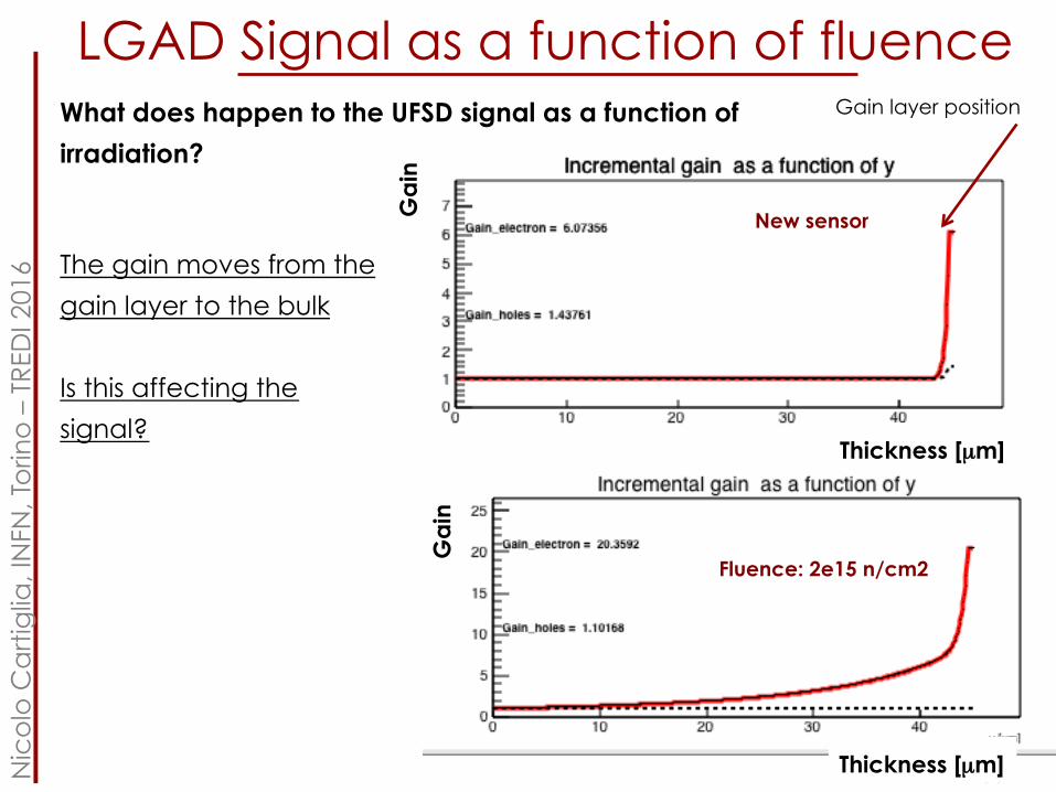
LGAD Signal as a function of fluence What does happen to the UFSD signal as a function of
irradiation?
New sensor
Fluence: 2e15 n/cm2
Ga
in
Ga
in
Thickness [µm]
Thickness [µm]
Gain layer position
The gain moves from the
gain layer to the bulk
Is this affecting the
signal?
12 Nic
olo
Ca
rtig
lia, I
NFN
, To
rino
– T
RED
I 201
6
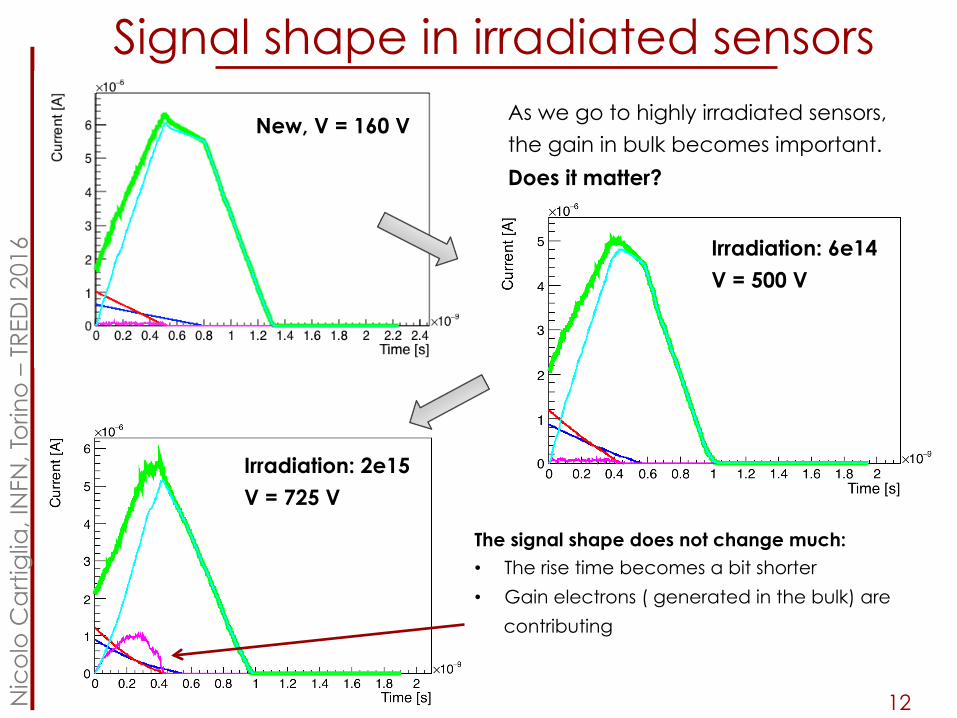
Signal shape in irradiated sensors
Irradiation: 6e14 V = 500 V
Irradiation: 2e15 V = 725 V
New, V = 160 V
The signal shape does not change much: • The rise time becomes a bit shorter
• Gain electrons ( generated in the bulk) are
contributing
As we go to highly irradiated sensors,
the gain in bulk becomes important.
Does it matter?
13 Nic
olo
Ca
rtig
lia, I
NFN
, To
rino
– T
RED
I 201
6
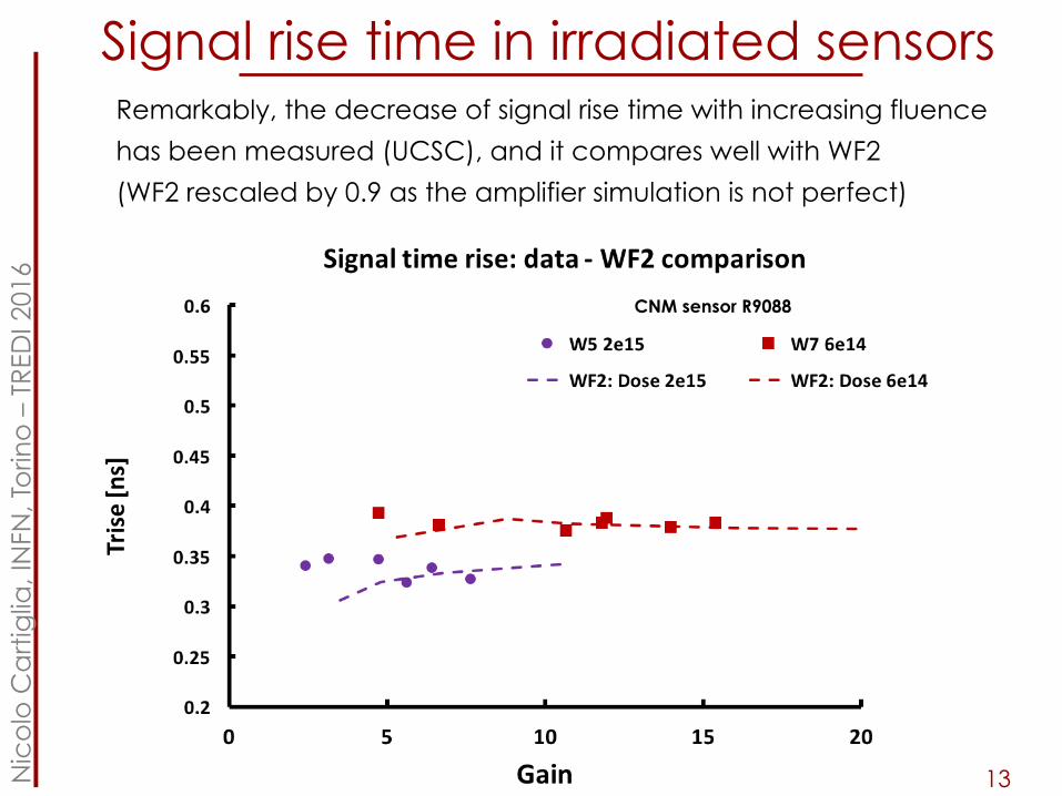
Signal rise time in irradiated sensors Remarkably, the decrease of signal rise time with increasing fluence
has been measured (UCSC), and it compares well with WF2
(WF2 rescaled by 0.9 as the amplifier simulation is not perfect)
CNM sensor R9088
14 Nic
olo
Ca
rtig
lia, I
NFN
, To
rino
– T
RED
I 201
6
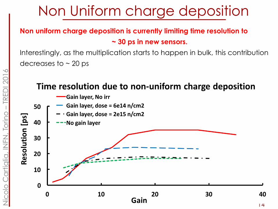
Non Uniform charge deposition Non uniform charge deposition is currently limiting time resolution to
~ 30 ps in new sensors.
Interestingly, as the multiplication starts to happen in bulk, this contribution
decreases to ~ 20 ps
15 Nic
olo
Ca
rtig
lia, I
NFN
, To
rino
– T
RED
I 201
6
Discussion point for LGADs CNM 300, 50 micron, epi and FZ substrates.
FBK 300 micron
HPK 50, 80 micron
Borders:
Number of guard rings, p-stops, edge termination
Gain layer implant type:
Shallow, deep, very deep, epi
Bulk-Support Wafer:
SOI, Si-Si, mostly very high resistivity bulk, few epi substrate
Leakage current:
Why is higher than we expect? Silicon quality? Support wafer?
Gain:
Sensor gain is very “power efficient”, we need to keep it ~ 20, otherwise
the electronics will require too much power
Dimension
1mm2, 2 mm2 diodes
What are the consequences of these differences?
Best Solution?
16 Nic
olo
Ca
rtig
lia, I
NFN
, To
rino
– T
RED
I 201
6
Acknowledgments
We kindly acknowledge the following funding agencies, collaborations: ! INFN - Gruppo V ! Horizon 2020, grant UFSD669529 ! Horizon 2020, grant INFRAIA ! Ministero degli Affari Esteri, Italy,MAE, “Progetti di Grande
Rilevanza Scientifica” ! U.S. Department of Energy grant number DE-SC0010107 ! CNM, Barcellona ! RD50, CERN
17 Nic
olo
Ca
rtig
lia, I
NFN
, To
rino
– T
RED
I 201
6
Conclusion We have compared measured data with 4 simulation models for 3
quantities: (i) Gain vs Vbias (LGAD), (ii) vs Temperature (LGAD) and (iii)
vs Vbias (PIN) and found that only the Massey model is able to fit
correctly all of them.
WF2 with a parameterization using Gregor’s data on Initial Acceptor
removal rate is able to correctly simulate the evolution of gain vs
fluence.
The evolution of the pulse shape with fluence is well explained by CCE,
the onset of gain in the bulk and the decrease of gain in the gain layer.
The contribution of charge non uniformity to time resolution decreases
with increasing gain in the bulk.

18 Nic
olo
Ca
rtig
lia, I
NFN
, To
rino
– T
RED
I 201
6
Extra
19 Nic
olo
Ca
rtig
lia, I
NFN
, To
rino
– T
RED
I 201
6
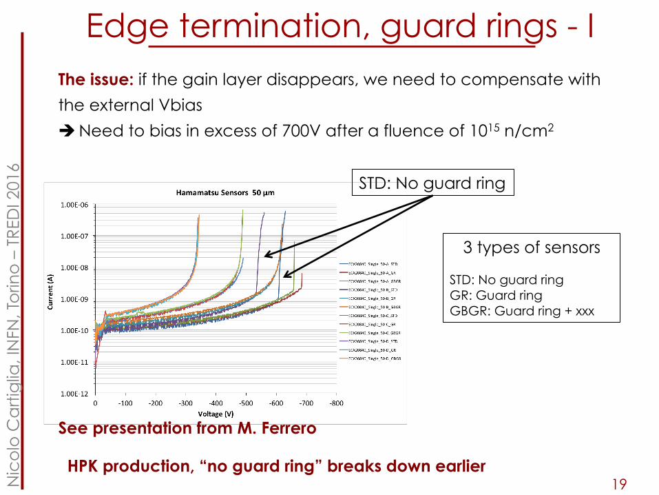
Edge termination, guard rings - I The issue: if the gain layer disappears, we need to compensate with
the external Vbias
" Need to bias in excess of 700V after a fluence of 1015 n/cm2
3 types of sensors
STD: No guard ring GR: Guard ring GBGR: Guard ring + xxx
HPK production, “no guard ring” breaks down earlier
STD: No guard ring
See presentation from M. Ferrero
20 Nic
olo
Ca
rtig
lia, I
NFN
, To
rino
– T
RED
I 201
6
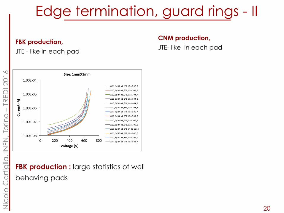
Edge termination, guard rings - II
FBK production, JTE - like in each pad
FBK production : large statistics of well
behaving pads
CNM production, JTE- like in each pad
21 Nic
olo
Ca
rtig
lia, I
NFN
, To
rino
– T
RED
I 201
6
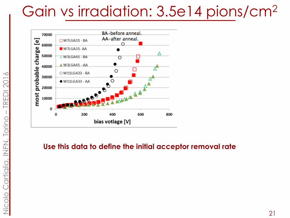
Gain vs irradiation: 3.5e14 pions/cm2
Use this data to define the initial acceptor removal rate
Recommended